J. Micromech. Microeng. 6 (1996) 385–397. Printed in the UK Stiction in surface micromachining Niels Tas†, Tonny Sonnenberg, Henri Jansen, Rob Legtenberg and Miko Elwenspoek MESA Research Institute, University of Twente, PO Box 217, 7500 AE Enschede, The Netherlands Received 29 August 1996 Abstract. Due to the smoothness of the surfaces in surface micromachining, large adhesion forces between fabricated structures and the substrate are encountered. Four major adhesion mechanisms have been analysed: capillary forces, hydrogen bridging, electrostatic forces and van der Waals forces. Once contact is made adhesion forces can be stronger than the restoring elastic forces and even short, thick beams will continue to stick to the substrate. Contact, resulting from drying liquid after release etching, has been successfully reduced. In order to make a fail-safe device stiction during its operational life-time should be anticipated. Electrostatic forces and acceleration forces caused by shocks encountered by the device can be large enough to bring structures into contact with the substrate. In order to avoid in-use stiction adhesion forces should therefore be minimized. This is possible by coating the device with weakly adhesive materials, by using bumps and side-wall spacers and by increasing the surface roughness at the interface. Capillary condensation should also be taken into account as this can lead to large increases in the contact area of roughened surfaces. 1. Introduction Stiction is a notorious cause of malfunctioning in microdevices. Surface micromachined structures which have been fabricated using the wet sacrificial layer etching technique can be pulled down to the substrate by capillary forces during drying [1, 2]. In recent years, much attention has been paid to avoiding contact during drying. Section 4 gives an overview of the methods which have been developed. Analysis of the adhesion mechanisms [3, 4] shows that stiction may occur whenever flexible and smooth structures are brought in contact with the substrate (sections 2 and 3). Therefore, in-use stiction should be anticipated. In section 5, two possible causes of contact during the operation of devices are analyzed: electrostatic attraction and acceleration forces. Incidental contact during operation can not always be excluded. Furthermore, devices are made where contact between moving parts is desirable [5, 6]. It is important to minimize adhesion forces in this case either by reducing the contact area or by changing the surface properties. This is analyzed in section 6. In section 6 results of stiction reduction by using self-aligned robust side-wall spacers are also presented. 2. Origins of stiction Adhesion of contacting surfaces has been studied extensively in tribology. Stiction phenomena are observed in hard-disk systems where the roughness of the contacting surfaces approaches nanometer scale. Adhesion † email: [email protected]. mechanisms have also been studied for wafer bonding purposes where stiction of contacted surfaces is desirable. Surface roughness plays an important role in adhesion. Surface micromachined structures are often very flat. Legtenberg [7] measured an RMS roughness between 1 and 3 nm at the bottom of released structures, depending on polysilicon and sacrificial (PECVD) silicon oxide thicknesses. The roughness of silicon wafer surfaces has been measured for bonding purposes. RMS roughness is typically below 1 nm [8, 9]. The real contact area (RCA) can be a large fraction of the apparent contact area between these structures. In the first analysis of adhesion mechanisms, we assume that the contacting surfaces are perfectly flat. The influence of surface roughness will be analyzed in section 6.3. Four adhesion mechanisms, which play an important role in stiction of surface micromachined structures, are discussed: capillary forces, hydrogen bridging, electrostatic forces and van der Waals forces [7]. 2.1. Capillary forces A thin liquid layer between two solid plates can work as an adhesive. If the contact angle θ C between liquid and solid is less than 90 ◦ (figure 1), the pressure inside the liquid drop will be lower than outside and a net attractive force between the plates exists. The pressure difference 1p la at the liquid–air interface is given by the Laplace equation [10]: 1p la = γ la r (1) 0960-1317/96/040385+13$19.50 c 1996 IOP Publishing Ltd 385
Transcript
J. Micromech. Microeng. 6 (1996) 385–397. Printed in the UK
Stiction in surface micromachining
Niels Tas †, Tonny Sonnenberg, Henri Jansen, Rob Legtenbergand Miko Elwenspoek
MESA Research Institute, University of Twente, PO Box 217, 7500 AE Enschede,The Netherlands
Received 29 August 1996
Abstract. Due to the smoothness of the surfaces in surface micromachining, largeadhesion forces between fabricated structures and the substrate are encountered.Four major adhesion mechanisms have been analysed: capillary forces, hydrogenbridging, electrostatic forces and van der Waals forces. Once contact is madeadhesion forces can be stronger than the restoring elastic forces and even short,thick beams will continue to stick to the substrate. Contact, resulting from dryingliquid after release etching, has been successfully reduced. In order to make afail-safe device stiction during its operational life-time should be anticipated.Electrostatic forces and acceleration forces caused by shocks encountered by thedevice can be large enough to bring structures into contact with the substrate. Inorder to avoid in-use stiction adhesion forces should therefore be minimized. Thisis possible by coating the device with weakly adhesive materials, by using bumpsand side-wall spacers and by increasing the surface roughness at the interface.Capillary condensation should also be taken into account as this can lead to largeincreases in the contact area of roughened surfaces.
1. Introduction
Stiction is a notorious cause of malfunctioning inmicrodevices. Surface micromachined structures whichhave been fabricated using the wet sacrificial layer etchingtechnique can be pulled down to the substrate by capillaryforces during drying [1, 2]. In recent years, much attentionhas been paid to avoiding contact during drying. Section 4gives an overview of the methods which have beendeveloped. Analysis of the adhesion mechanisms [3, 4]shows that stiction may occur whenever flexible andsmooth structures are brought in contact with the substrate(sections 2 and 3). Therefore, in-use stiction should beanticipated. In section 5, two possible causes of contactduring the operation of devices are analyzed: electrostaticattraction and acceleration forces. Incidental contact duringoperation can not always be excluded. Furthermore,devices are made where contact between moving partsis desirable [5, 6]. It is important to minimize adhesionforces in this case either by reducing the contact area orby changing the surface properties. This is analyzed insection 6. In section 6 results of stiction reduction by usingself-aligned robust side-wall spacers are also presented.
2. Origins of stiction
Adhesion of contacting surfaces has been studiedextensively in tribology. Stiction phenomena areobserved in hard-disk systems where the roughness of thecontacting surfaces approaches nanometer scale. Adhesion
mechanisms have also been studied for wafer bondingpurposes where stiction of contacted surfaces is desirable.Surface roughness plays an important role in adhesion.Surface micromachined structures are often very flat.Legtenberg [7] measured an RMS roughness between 1and 3 nm at the bottom of released structures, dependingon polysilicon and sacrificial (PECVD) silicon oxidethicknesses. The roughness of silicon wafer surfaces hasbeen measured for bonding purposes. RMS roughnessis typically below 1 nm [8, 9]. The real contact area(RCA) can be a large fraction of the apparent contactarea between these structures. In the first analysis ofadhesion mechanisms, we assume that the contactingsurfaces are perfectly flat. The influence of surfaceroughness will be analyzed in section 6.3. Four adhesionmechanisms, which play an important role in stiction ofsurface micromachined structures, are discussed: capillaryforces, hydrogen bridging, electrostatic forces and van derWaals forces [7].
2.1. Capillary forces
A thin liquid layer between two solid plates can work as anadhesive. If the contact angleθC between liquid and solidis less than 90◦ (figure 1), the pressure inside the liquiddrop will be lower than outside and a net attractive forcebetween the plates exists.
The pressure difference1pla at the liquid–air interfaceis given by the Laplace equation [10]:
Figure 1. A thin layer of liquid working as an adhesivebetween two plates. θC is the contact angle between liquidand solid in air, g is the liquid layer thickness, and A is thewetted area. A force F is applied to maintain equilibrium.
whereγla is the surface tension of the liquid–air interface,and r is the radius of curvature of the meniscus (negativeif concave). In figure 1, the liquid is between the platesand the liquid contacts the solid at the fixed contact angle.From simple geometry it follows thatr = −g/2 cosθC . Inequilibrium, an external forceF separating the plates mustbe applied to counterbalance the capillary pressure forces:
F = −1plaA = 2Aγla cosθC
g(2)
whereA is the wetted area. Note that a positive forceF
corresponds to a negative Laplace pressure. The pressureinside the liquid is lower than outside and the plates arepushed together by pressure forces. For stiction calculationsit is convenient to calculate the surface energy stored at theinterface that is bridged by a drop of liquid [2]. Considera drop of liquid placed on a solid, surrounded by air(figure 2). In equilibrium, the contact angle between liquidand solid is determined by the balance between the surfacetensions of the three interfaces. This balance is expressedby Young’s equation [10]:
γsa = γsl + γla cosθC 0 < θC < π (3)
whereγsa is the surface tension of the solid–air interfaceandγsl is the surface tension of the solid–liquid interface.Young’s equation is also valid for configurations other thanthat of figure 2. The contact angle is the same on a curvedor irregular shaped surface, inside a capillary etc.
If the solid–air surface tension is smaller than the sumof the liquid–air and solid–liquid surface tensions, then thecontact angle is larger than 0◦ and the liquid will be non-spreading (figure 3).
If the solid–air surface tension is larger than the sumof the liquid–air and solid–liquid surface tensions, then itwill be energetically favorable for the liquid to spread. Thecontact angle will be equal to 0◦. A drop bridging twosurfaces will form thin liquid films outside the bridged area(figure 4).
Figure 2. Liquid drop (L) on a solid (S), in air (A). θC is thecontact angle between liquid and solid in air.
Figure 3. Liquid bridging two solids. The liquid isnon-spreading. The solid is only covered in the bridgedarea Ab . At is the total facing area.
Figure 4. Liquid bridging two solids. The liquid isspreading. Outside the bridged area Ab , a thin liquid filmcovers the solid.
The total surface energy of the area between the platescan be calculated by adding the surface tensions of thesolid–air, solid–liquid and liquid–air interfaces [2]. It isassumed that the liquid is confined to a bridged areaAb,which is smaller than or equal to the total facing areasAt .(4a) expresses the surface energy in the case of a spreadingliquid, (4b) that for a non-spreading liquid:
Es = 2[At
(γsl + γla
) − Abγla
] = 2[At
(γsl
+γla
) − Abγla cosθC
](4a)
Es = [Atγsa − Ab
(γsa − γsl
)] = 2[Atγsa
−Abγla cosθC
]. (4b)
In (4a, b) the energy of the liquid–air meniscus area isneglected, which is a fair assumption if the gapg betweenthe plates is small, so that the meniscus area is smallcompared to the bridged area. The total areaAt and thesurface tensions are constant. Therefore, the total surfaceenergy as a function of the bridged area can be written in
386
Stiction in surface micromachining
Figure 5. Capillary condensation between two contactingsurfaces. The meniscus curvatures are equal to the Kelvinradius; the contact angles satisfy Young’s equation.
a general form, which is valid for both the spreading andthe non-spreading condition [2]:
Es = C − 2Abγla cosθC (4c)
whereγla cosθC is the adhesion tension, andC takes intoaccount the constant terms in (4a, b). The importanceof liquid mediated adhesion is supported by both stictionand friction experiments. Stiction of released structurescan show a large dependence on the relative humidityof air [11]. Friction measurements of silicon and siliconcompounds [12] show a strong dependence of the staticfriction coefficient on relative humidity. In macrotribologyit is well known that adhesion of solids can stronglydepend on relative humidity [13]. This is caused bycapillary condensation. Liquids that wet or have a smallcontact angle on surfaces will spontaneously condense intocracks, pores, and into small gaps surrounding the pointsof contact between the contacting surfaces. At equilibriumthe meniscus curvature is equal to theKelvin radius[10]:
rK = γlaV
RT log(p/ps)(5)
whereV is the molar volume,p is the vapor pressure andps is the saturation vapor pressure. At room temperature,γlaV/(RT ) = 0.54 nm for water [10]. The meniscuscurvature strongly depends on the relative vapor pressurep/ps . For a relative humidity of 50% we find log(p/ps) =−0.69 and rk = −0.8 nm. At 100% relative humidity,log(p/ps) = 0 andrk = ∞ which means that a water filmcan grow all over the surface. The amount of condensedliquid in thermodynamic equilibrium is determined by boththe Kelvin radius and the contact angle. The meniscuscurvatures are equal to the Kelvin radius and the contactangles satisfy Young’s equation (figure 5).
Capillary condensation can lead to a large increase inthe RCA of solids by means of liquid bridging. It can,therefore, drastically increase the adhesion of those solidsthat due to their roughness show a low adhesion in a dryenvironment [13]. Models for the adhesion force due tocapillary condensed liquid have been developed in hard-disk tribology [14–16].
2.2. Hydrogen bridging
Hydrophilic silicon surfaces, under atmospheric conditionsand temperatures well below 200◦C, contain adsorbedwater layers. When two of these hydrated surfaces arebrought into close contact, hydrogen bonds may formbetween oxygen and the hydrogen atoms of the adsorbed
water layers. Stenglet al [17] have calculated an adhesionenergy of about 100 mJ m−2 based on this bondingmodel. From wafer bonding experiments [18, 19] andstiction experiments [4, 20], adhesion energies between 60and 270 mJ m−2 have been reported for hydrophilic surfaces(T < 200◦C).
2.3. Electrostatic forces between mobile charges
Electrostatic attractive forces across the interface can arisefrom a difference in work functions or from electrostaticcharging of opposed surfaces [21, 18, 22]. Difference inthe work function leads to the formation of an electricaldouble layer by a net transfer of electrons from one surfaceto the other. Contact potentials are generally below 0.5 V,and the resulting surface charge densities are smaller than1013 elementary charges per square centimetre [21]. Atsmall separations the electrostatic pressure between flatsurfaces is generally lower than the van der Waals pressure[21]. Temporary charging can occur during processing[22] or operation. Examples of this are tribocharging ofrubbing surfaces [15] and charge accumulation in insulatorsof electrostatic operated micromotors [23]. Permanentstiction is not expected due to these effects because thenon-equilibrium charging will relax in time.
2.4. Van der Waals forces
The van der Waals dispersion forces between two bodies arecaused by mutual electric interaction of the induced dipolesin the two bodies. Dispersion forces generally dominateover orientation and induction forces except for stronglypolar molecules [24]. The interaction energy per unit areadue to van der Waals interaction between two flat surfacesin the non-retarded regime (d < 20 nm) is given by [10]
EvdW = − A
12πd2(6)
where A is the Hamaker constant andd is the distancebetween the surfaces. For most solids and liquids, theHamaker constant lies in the range 0.4–4× 10⁻¹⁹ J [10].For surfaces in contact a cut-off distance ofd = d0,slightly smaller than the interatomic distance, should beused to calculate the adhesion energy. Using a universalcut-off distance ofd0 = 0.165 nm and Hamaker constantscalculated by the Lifshitz theory, a good agreement betweenexperimental values and adhesion energies calculated withequation (6) is found for non-hydrogen-bonding, non-metallic solids and liquids [10]. Equation (6) withd = d0
can be used to predict the adhesion energy of a cleanhydrophobic silicon surface. However, the adhesion energystrongly depends on the surface termination. Often this isnot exactly known. For pure silicon a Hamaker constantof 1.1 × 10⁻¹⁸ J is given [21], yielding a adhesion energyof 1.1 J m−2 [10]. From wafer bonding literature [18]and stiction experiments [3, 20], adhesion energies between12 and 140 mJ m−2 are reported. The reported valuesmay be much lower than the theoretical value due tohydrogen, fluorine or CHx termination of the surface [18]and due to surface roughness. Compared to hydrophilic
387
N Tas et al
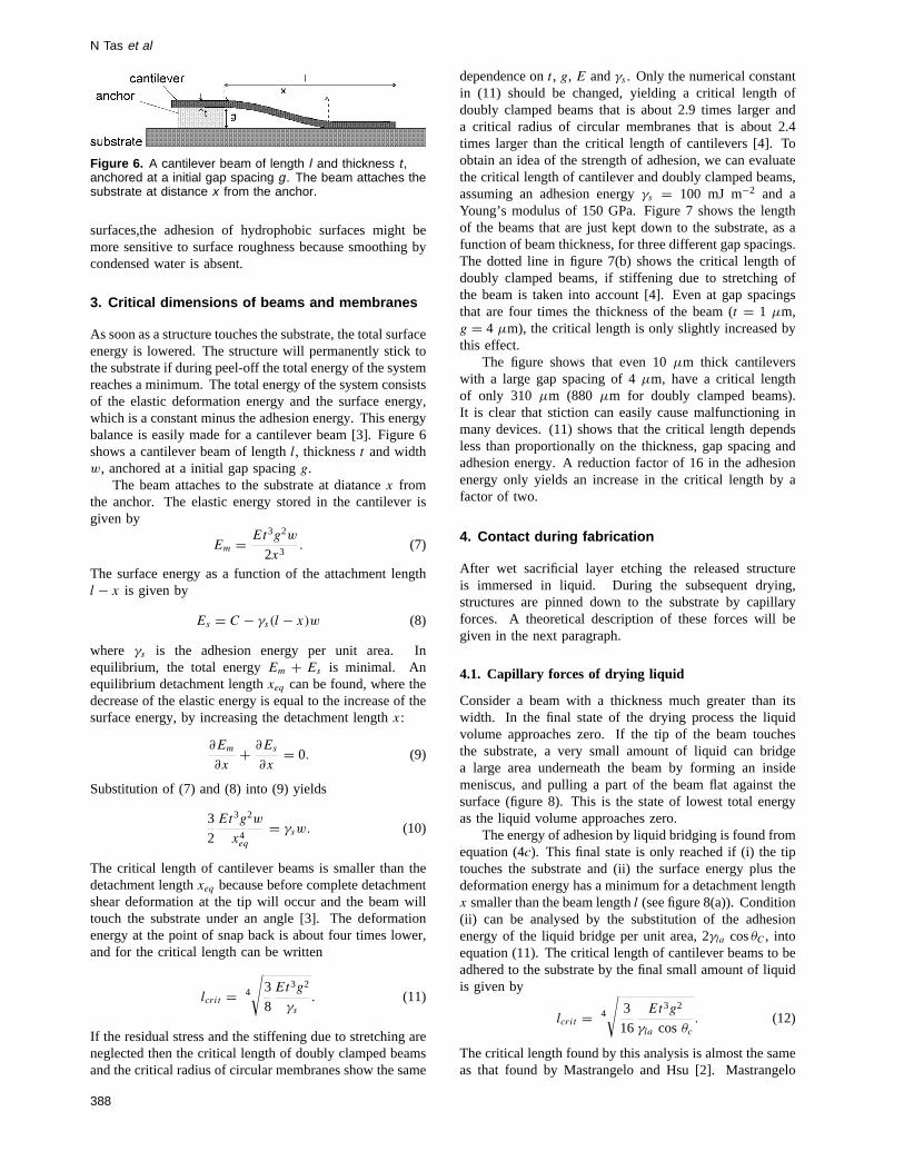
Figure 6. A cantilever beam of length l and thickness t ,anchored at a initial gap spacing g . The beam attaches thesubstrate at distance x from the anchor.
surfaces,the adhesion of hydrophobic surfaces might bemore sensitive to surface roughness because smoothing bycondensed water is absent.
3. Critical dimensions of beams and membranes
As soon as a structure touches the substrate, the total surfaceenergy is lowered. The structure will permanently stick tothe substrate if during peel-off the total energy of the systemreaches a minimum. The total energy of the system consistsof the elastic deformation energy and the surface energy,which is a constant minus the adhesion energy. This energybalance is easily made for a cantilever beam [3]. Figure 6shows a cantilever beam of lengthl, thicknesst and widthw, anchored at a initial gap spacingg.
The beam attaches to the substrate at diatancex fromthe anchor. The elastic energy stored in the cantilever isgiven by
Em = Et3g2w
2x3. (7)
The surface energy as a function of the attachment lengthl − x is given by
Es = C − γs(l − x)w (8)
where γs is the adhesion energy per unit area. Inequilibrium, the total energyEm + Es is minimal. Anequilibrium detachment lengthxeq can be found, where thedecrease of the elastic energy is equal to the increase of thesurface energy, by increasing the detachment lengthx:
∂Em
∂x+ ∂Es
∂x= 0. (9)
Substitution of (7) and (8) into (9) yields
3
2
Et3g2w
x4eq
= γsw. (10)
The critical length of cantilever beams is smaller than thedetachment lengthxeq because before complete detachmentshear deformation at the tip will occur and the beam willtouch the substrate under an angle [3]. The deformationenergy at the point of snap back is about four times lower,and for the critical length can be written
lcrit = 4
√3
8
Et3g2
γs
. (11)
If the residual stress and the stiffening due to stretching areneglected then the critical length of doubly clamped beamsand the critical radius of circular membranes show the same
dependence ont , g, E andγs . Only the numerical constantin (11) should be changed, yielding a critical length ofdoubly clamped beams that is about 2.9 times larger anda critical radius of circular membranes that is about 2.4times larger than the critical length of cantilevers [4]. Toobtain an idea of the strength of adhesion, we can evaluatethe critical length of cantilever and doubly clamped beams,assuming an adhesion energyγs = 100 mJ m−2 and aYoung’s modulus of 150 GPa. Figure 7 shows the lengthof the beams that are just kept down to the substrate, as afunction of beam thickness, for three different gap spacings.The dotted line in figure 7(b) shows the critical length ofdoubly clamped beams, if stiffening due to stretching ofthe beam is taken into account [4]. Even at gap spacingsthat are four times the thickness of the beam (t = 1 µm,g = 4 µm), the critical length is only slightly increased bythis effect.
The figure shows that even 10µm thick cantileverswith a large gap spacing of 4µm, have a critical lengthof only 310 µm (880 µm for doubly clamped beams).It is clear that stiction can easily cause malfunctioning inmany devices. (11) shows that the critical length dependsless than proportionally on the thickness, gap spacing andadhesion energy. A reduction factor of 16 in the adhesionenergy only yields an increase in the critical length by afactor of two.
4. Contact during fabrication
After wet sacrificial layer etching the released structureis immersed in liquid. During the subsequent drying,structures are pinned down to the substrate by capillaryforces. A theoretical description of these forces will begiven in the next paragraph.
4.1. Capillary forces of drying liquid
Consider a beam with a thickness much greater than itswidth. In the final state of the drying process the liquidvolume approaches zero. If the tip of the beam touchesthe substrate, a very small amount of liquid can bridgea large area underneath the beam by forming an insidemeniscus, and pulling a part of the beam flat against thesurface (figure 8). This is the state of lowest total energyas the liquid volume approaches zero.
The energy of adhesion by liquid bridging is found fromequation (4c). This final state is only reached if (i) the tiptouches the substrate and (ii) the surface energy plus thedeformation energy has a minimum for a detachment lengthx smaller than the beam lengthl (see figure 8(a)). Condition(ii) can be analysed by the substitution of the adhesionenergy of the liquid bridge per unit area, 2γla cosθC , intoequation (11). The critical length of cantilever beams to beadhered to the substrate by the final small amount of liquidis given by
lcrit = 4
√3
16
Et3g2
γla cosθc
. (12)
The critical length found by this analysis is almost the sameas that found by Mastrangelo and Hsu [2]. Mastrangelo
388
Stiction in surface micromachining
(a)
(b)
Figure 7. Critical lengths of cantilever beams (a) anddoubly clamped beams (b), as a function of beam thicknessfor different gap spacings, according to equation (11). AYoung’s modulus of 150 GPa and an adhesion energy of100 mJ m−2 is assumed. Residual stress is neglected. Thedotted line in (b) shows the critical length of doublyclamped beams if stiffening due to stretching of the beamis taken into account [4]. Beams shorter than the criticallength will snap back after contacting the substrate.
(a)
(b)
Figure 8. Final state of liquid drying underneath acantilever beam: (a) side view; (b) front view. In the finalstate of drying a small amount of liquid can lower thesurface energy by a great amount by bridging an area thatis pulled flat against the substrate.
and Hsu modeled the complete drying trajectory to find outwhether the tip would touch or not. If residual stresses
(a)
(b)
Figure 9. (a) Pull-down of a cantilever beam byelectrostatic forces. U is the applied voltage differencebetween the beam and the substrate, g is the initial gapspacing, l is the length of the beam, t is the thickness andy is the tip deflection. (b) The shaded region is the gap forwhich the capacitance is calculated.
and stiffening due to stretching are neglected, then thecritical length of doubly clamped beams is about 2.5 timeslarger and the critical radius of circular membranes isabout 1.7 times larger [2]. The critical length during peel-off calculated using (11) assuming an adhesion energy of100 mJ m−2 and the critical length during drying calculatedusing (12) assuming an adhesion energy of 146 mJ m−2
(water; 20◦C; 0◦ contact angle) are almost identical.Therefore figure 7(a) also applies to the latter case. Thecritical length of silicon cantilevers during the drying ofwater, assuming a thicknesst = 5 µm, a Young’s modulusE = 150 GPa and a gap spacingg = 2 µm, equals 119µm.This is too small for most applications. Pinning down canoccur at significantly smaller lengths if structures are largeat the tip and small at the base.
4.2. How to avoid contact during drying
Unless very thick or short structures and large gap spacingsare used, it is not possible to avoid contact during dryingby increasing the elastic deformation energy. Structuresthat stick can sometimes be released mechanically or bygenerating an repulsive force between the structures [25].However, these methods do not seem to be suitable forbatch processing. In general, it is more practical toavoid contact during the drying process. In the past7 years different methods have been developed that allowfabrication of structures with thickness:length ratios of morethan 1:1000.
The adhesion tensionγla cosθc can be decreasedchoosing a low-surface-tension liquid for drying [11, 26],or by adjusting the contact angle. Scheeperset al [11]report reduction of the stiction of silicon nitride beams afterdrying from n-hexane, which has a low surface tension(19 mJ m−2) compared to DI water (73 mJ m−2). Bychanging the combination of the surface materials and theliquid to be dried, one can try to obtain a contact anglenear or over 90◦. Only small negative, or even repulsivecapillary pressures, result [27]. Abeet al [28], have tried toincrease yield by drying at elevated temperatures becausesurface tensions decrease on increasing temperature. Anadditional mechanism of stiction reduction when drying at
389
N Tas et al
high temperatures may be cavitation in the liquid bridge[13, 29]. If the vapor pressure at the drying temperatureexceeds the pressure inside the liquid bridge (the pressureoutside plus the Laplace pressure), the liquid may start toboil locally [13]. This will limit the negative capillarypressure.
Several methods have been proposed that applytemporary supportto counteract the surface tensional forcesduring drying. Break-away polysilicon supports are usedthat have to be removed after release processing [30, 31].This can be done mechanically (probing) or by meltingthe supports [31]. Because the supports have to beremoved one by one, application is limited to experimentaldevices. Batch-processing-compatible temporary supportshave therefore been developed [32, 33]. In both methodsholes in the sacrificial layer are made to anchor thestructures to be released to the substrate. Anchoring isachieved using a photoresist grid [33] or using polymercolumns [32]. The maximum spacing between the supportsis determined by the stiffness of the structures to be released[32]. After a complete sacrificial layer etch the supportsare removed in oxygen plasma. Temporary supports arevery effective in avoiding contact during drying. Forexample, Mastrangelo and Saloka [32] have fabricatedplates measuring 3000×3000×1 µm3 (1 µm gap spacing).
The drying process and its capillary forces can beavoided by using another physical process to get rid of theliquid. In the ordinary drying process, liquid evaporates andcapillary forces arise as a result of the surface tension of theliquid–vapor interface. In thesupercritical dryingprocess,first reported by Mulhernet al [34], liquid is transferredto vapor via the supercritical phase. Carbon dioxide isused because of its low critical temperature and pressure(Tc = 31.1 ◦C, pc = 72.8 atm). During evaporation ofthe supercritical carbon dioxide, no liquid–vapor interfaceexists, so there are no capillary forces working. Beams witha length of 850µm (1.4 µm thick, 2.7µm gap spacing)have been released [34].Freeze dryingas a liquid removingstep was first applied to micromachining by Guckelet al[1]. After HF etch, the wafer is immersed in a water–methanol mixture. Next, the liquid surrounding the waferis frozen by evaporation cooling in a vacuum chamber.The solid water–methanol is removed by sublimation at0.15 mbar. The methanol has been added to avoidsupercooling of the water as this can cause the water tofreeze too rapidly. At MESA we now use sublimationof cyclohexane at about−5 ◦C [7]. The sublimation isperformed at atmosperic pressure on a plate cooled by aPeltier element under a continuous flow of nitrogen. Thenitrogen flow aids the sublimation process by removing thecyclohexane vapor. It also prevents condensation of wateron the substrate. For the same reason the wafer is heatedto room temperature after completion of the sublimationprocess. High-yield fabrication of cantilevers up to 1 mm inlength (2µm thick; 2µm gap spacing) has been achieved.
Orpana and Korhonen [35] report the use ofpolymersupportto avoid pull-down by drying liquid. After the HFetch a rinsing process starts in which the HF is graduallysubstituted by organic solvent. Finally the wafers areimmersed in a photoresist–acetone mixture. The photoresist
is solidified and can be stripped in a oxygen plasma.Kozlowski et al [36] developed a rinsing procedure inwhich the structures are finally immersed in divinylbenzene.This monomer is then solidified by polymerization underUV light. The release is completed by stripping the polymerin a oxygen plasma. High-yield release of 500µm long(500 nm thick: 900 nm gap spacing) cantilevers has beenaccomplished [36].
Methods that use adry sacrificial etchstep avoid theuse of liquid completely. Silicon dioxide can be removedby etching in HF vapor [27]. Long (2 mm) thin beams havebeen successfully released. The SCREAM process [37], aswell as theBSM-one run[38] apply sacrificial layer etchingof (poly)silicon. The SIMPLE process applies sacrificiallayer etching of n+ doped silicon [39]. A characteristicproblem of these processes is the limited width of structuresthat can be underetched. Dry sacrificial layer etching ispromising, especially when alternative structural materialsand sacrificial layers [40] are considered.
5. Contact during operation
Stiction originating from the fabrication process has beenreduced quite successfully. Fail-safe devices should bedesigned to avoid stiction of released structures during theiroperational life-time. Sources of contact strongly depend onthe application of the device. An analysis of two possiblesource of in-use contact, electrostatic pull-down and push-down by acceleration forces, follows.
5.1. Electrostatic pull-down
To further our understanding of the effect of electrostaticforces, we will firstly examine cantilever beams due to avoltage difference between the beams and the substrate, arepulled down to the substrate. The deflection of the beam isdescribed by the following non-linear differential equation:
El∂4y(x)
∂x4= εwU2
2(g − y(x))2(13)
where y(x) is the deflection at positionx along thecantilever,g is the initial gap to the substrate,El is theflexural rigidity of the beam,ε is the permittivity,w is thewidth of the beam andU is the voltage difference betweenthe beam and the substrate (figure 9). A full analyticalsolution can not yet be obtained. An approximate solutioncan be derived by looking at the total potential energywhich consists of the electrical energy stored in the gapand the mechanical deformation energy stored in the beam.This can easily be done if a constant shape is assumed.The deflection function can only change in amplitude. Theelastic deformation energy assuming the uniform load shapeis a function of the tip deflectiony:
Em = 48
30
El
l3y2. (14)
The capacitance between the beam and the substrate iscalculated by assuming a linear shape between the tip andthe anchor of the beam (figure 9(b)):
C(y) = εwl
yln
∣∣∣∣ g
g − y
∣∣∣∣. (15)
390
Stiction in surface micromachining
Tip deflection as a function of the applied voltageU
can be found from the balance between the electrostaticpull-down force and the restoring elastic force:
∂Em
∂y= ∂Ee
∂y(16)
whereEe = 12C(y)U2. The system becomes instable (pull-
in) if the pull-down force increases faster than the restoringelastic force with increasingy. The point of instability istherefore reached if
∂2Em
∂y2= ∂2Ee
∂y2. (17)
Combination of equations (15)–(17) yields for the tipdeflection at pull-in
lng
g − y= y(g − 4
3y)
(g − y)2(18)
which givesypi = 0.44g. Substitution in equation (16) andcombination with equation (14) gives for the pull-in voltage
Upi =√
0.22Eg3t3
εl4. (19)
(19) slightly underestimates the pull-in voltage, becausethe capacity is overestimated using the linear deflectionprofile. The same procedure can be applied to obtainthe pull-in gap and voltage for doubly clamped beams,neglecting the axial tensile stress. A convenient deflectionfunction is y(x) = (y/2)(1 − cos(2πx/l), wherey is thedeflection in the middle of the beam andl is the total length[41]. This way a pull-in deflection of25g is found. Anexpression similar to (19) is found for the pull-in voltageas a function oft , g, l and E. The numerical constantis equal to 12.1 instead of 0.22 andl is the total length ofthe doubly clamped beam. Accurate calculations have beenperformed by Osterberget al [42]. They found an analyticalsolution for beam and membrane pull-in voltages assuminga uniform load, and replaced the numerical constants in thissolution by fitting parameters, which were obtained fromnumerical solutions of the differential equations. This waythe non-uniform electrostatic load working on the deflectedbeam or membrane could be taken into account. In [42] theinfluence of residual stress and stiffening due to stretchingof the doubly clamped beam and the membrane on the pull-in voltage are incorporated in the model. If these effectsare neglected a general expression for the pull-in voltage ofcantilevers, doubly clamped beams and membranes similarto (19) is found [42]:
Upi =√
cEg3t3
εl4(20)
wherel represents the total length in the case of cantileverand doubly clamped beams, and the radius in the case of acircular membrane. The value forc according to Osterberget al [42], for the three configurations, is given in table 1.
Figure 10 shows pull-in voltages of cantilever beamsas a function ofl for different beam thicknesses and initialgaps according to (19). A cantilever with a length of
Table 1. The numerical value for c to be used in (20) forcantilevers, doubly clamped beams and circularmembranes [42].
a For circular membranes an effectiveYoung’s modulus E/(1 − ν2) should be usedin (20), where ν is the Poisson ratio.
Figure 10. Pull-in voltage for a cantilever beam as afunction of the length: (a) thickness t = 1 µm, initial gapspacing g = 1 µm; (b) t = 5 µm, g = 2 µm; (c) g = 4 µm,t = 10 µm.
Figure 11. A cantilever beam deflecting under its ownweight. Assume that the substrate is accelerated upwardby a (m s−2). The beam is loaded by a force q per unitlength of ρawt , where ρ is the density, w is the width of thebeam and t is the thickness of the beam.
100 µm, a thickness of 1µm and a gap spacing of 1µmis pulled to the substrate by a voltage difference of only6.1 V. In electrostatic actuators voltages of up to 100 V arecommon. Vertical pull-in has to be anticipated in the designeven if thick structures (10µm) and large gap spacings(4 µm) are used (figure 10). Pull-in to the substrate canbe avoided by electrical shielding in order to give thesubstrate locally the same potential as the structures directlyabove. Another approach is to always keep rotor parts atthe same voltage as the substrate and to only allow a voltagedifference between the stator poles and the substrate.
391
N Tas et al
Figure 12. The length of silicon cantilever beamscollapsing under their own weight (a = 9.8 m s−2). At thecritical length, the tip just touches the substrate. A Young’smodulus of 150 GPa and a density of 2.3 × 10³ kg m−3 areassumed.
Figure 13. A cantilever beam carrying n times its ownmass at the tip. If the substrate is accelerated by a (m s−2)upward, the tip is pushed down to the substrate by a forcenρawtl .
5.2. Push-down by acceleration forces
First collapse of a cantilever under its own weight isanalyzed. Let us assume that the substrate is acceleratedby a (m s−2) in an upward direction. This means that acantilever beam, anchored on the substrate, is pushed downby a forceq per unit length ofρawt , whereρ is the density,w is the width of the beam andt is the thickness of thebeam (figure 11).
The tip deflection of the cantilever beam, uniformlyloaded by thisq is given by
y = ρwtal4
8El. (21)
ρ is the density,w is the width of the beam,t is thethickness of the beam,l is the length of the beam andEI is the flexural rigidity. By taking the tip deflection asequal to the gap spacingg, and substitutingI = t3w/12 forthe moment of inertia, we can write for the critical length
lcrit = 4
√2
3
gt2E
ρa. (22)
The critical length as a function of the beam thicknessfor silicon cantilevers undergoing Earth gravitationalacceleration is shown in figure 12.
The critical length of doubly clamped beams is 24√
3times larger (neglecting axial stress). For the dimensionsevaluated, critical lengths are all larger than 1 mm. Only
Figure 14. The critical length of silicon cantilever beamscarrying 100 times their own mass, undergoing verticalacceleration of 100 m s−2, as a function of the thickness t ,for three different gap spacings g . A Young’s modulus of150 GPa and a density of 2.3 × 10³ kg m−3 are assumed.
Figure 15. A photograph of a large comb-drive actuator[7]. Support springs are 1 mm long, and carry a large massat the tip.
for thin structures, suspended near the substrate, is therea danger of touching the substrate due to gravity. Largestructures are often supported by thin flexible springs. Inthis case, acceleration forces have to be taken seriously,especially if devices have to be shock proof. We thereforeanalyze a cantilever beam, loaded at its tip byn times itsown weight (figure 13).
Let us assume that the substrate is accelerated bya inan upward direction. With reference to the substrate, thiscan be modeled by loading the cantilever at its tip, by aforce of nρawtl. The tip deflectiony is given by
y = nρtwal4
3El. (23)
By taking the tip deflection as equal to the gap spacingg,and substitutingI = t3w/12 for the moment of inertia, we
392
Stiction in surface micromachining
Figure 16. Fabrication of bumps according to [48] and [49]: (a) isotropic etch of hole; (b) deposit of polysilicon structurallayer; (c) release etch.
Figure 17. A processing scheme for robust side-wall spacers, starting from (a) patterned silicon structural layer; (b) isotropicthinning of sacrificial layer; (c) growth of anti-stiction silicon nitride layer; (d) anisotropic silicon nitride etch; (e) sacrificial layeretch.
can write for the critical length
lcrit = 4
√gt2E
4nρa. (24)
The critical length of doubly clamped beams is 2√
2 timeslarger (neglecting axial stress). Figure 14 shows the criticallength of silicon cantilevers, carrying 100 times their ownmass, under an acceleration of 100 m s−2, which is only amoderate shock.
For thicknesses smaller than about 10µm, thecritical length is in the region which is often used inelastic suspensions of laterally driven electrostatic devices.Mechanical shock induced contact is difficult to eliminatefrom these devices.
6. Stiction reduction of contacting structures
In section 3 it was shown that an adhesion energy of100 mJ m−2 is high enough to counterbalance restoringelastic forces of short, thick beams. If large structures aresupported by narrow beams the stiction forces will be evenmore dominant. The comb-drive shown in figure 15 is anexample of such a structure. Structures like this are alsosensitive to applied mechanical shocks. It therefore requiresspecial fabrication procedures and careful handling duringits whole life-time. If stiction is to be eliminated in sucha large structure, extreme reduction of the adhesion energyis necessary. Low adhesion energy is also desirable indevices where contact between moving parts is essential tothe functioning of the device [5, 6]. Coating and reductionof the RCA is analyzed here.
6.1. Reducing the adhesion energy
Coating can have a significant effect if capillary forces orhydrogen bridging are the dominant adhesion mechanisms.By providing a hydrophobic surface, coating can eliminatewater mediated adhesion [43, 44]. Adhesion by van derWaals forces will always remain. A typical weakly
adhesive material such as PTFE still has a surface tensionof the order of 20 mJ m−2. Other weakly adhesive materialsare the typical friction reducing coatings [45–47]. Theadhesion energy of perfect flat surfaces will hardly be lowerthan about 40 mJ m−2. Coating alone will not be enoughif large reductions of the adhesion energy are desired.Reduction of the RCA should be applied.
6.2. Reducing the geometrical area contact
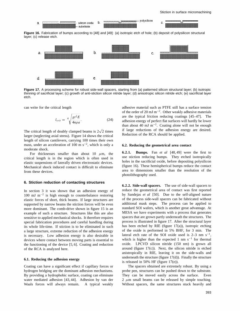
6.2.1. Bumps. Fan et al [48, 49] were the first touse stiction reducing bumps. They etched isotropicallyholes in the sacrificial oxide, before depositing polysilicon(figure 16). These hemispherical bumps reduce the contactarea to dimensions smaller than the resolution of thephotolithography used.
6.2.2. Side-wall spacers. The use of side-wall spacers toreduce the geometrical area of contact was first reportedby Sandejaset al [50]. Due to the self-aligned natureof the process side-wall spacers can be fabricated withoutadditional mask steps. The process can be applied tostandard SOI wafers, which is another great advantage. AtMESA we have experiments with a process that generatesspacers that are grown partly underneath the structures. Theprocess is illustrated in figure 17. After the structural layerhas been etched by RIE (figure 17(a)), isotropic etchingof the oxide is performed in 5% BHF, for 3 min. Thelateral etch rate of the SOI oxide used is 2–3 nm s−1,which is higher than the expected 1 nm s−1 for thermaloxide. LPCVD silicon nitride (150 nm) is grown allaround (figure 17(c)). Next, the silicon nitride is etchedanistropically in RIE, leaving it on the side-walls andunderneath the structure (figure 17(d)). Finally the structureis released in 50% HF (figure 17(e)).
The spacers obtained are extremely robust. By using aprobe pen, structures can be pushed down to the substrate.They can be moved easily across the surface. Even2 µm small beams can be released by simple touching.Without spacers, the same structures stuck heavily and
393
N Tas et al
(a)
(b)
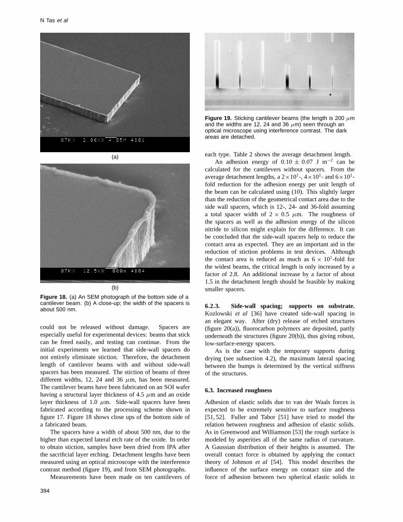
Figure 18. (a) An SEM photograph of the bottom side of acantilever beam. (b) A close-up; the width of the spacers isabout 500 nm.
could not be released without damage. Spacers areespecially useful for experimental devices: beams that stickcan be freed easily, and testing can continue. From theinitial experiments we learned that side-wall spacers donot entirely eliminate stiction. Therefore, the detachmentlength of cantilever beams with and without side-wallspacers has been measured. The stiction of beams of threedifferent widths, 12, 24 and 36µm, has been measured.The cantilever beams have been fabricated on an SOI waferhaving a structural layer thickness of 4.5µm and an oxidelayer thickness of 1.0µm. Side-wall spacers have beenfabricated according to the processing scheme shown infigure 17. Figure 18 shows close ups of the bottom side ofa fabricated beam.
The spacers have a width of about 500 nm, due to thehigher than expected lateral etch rate of the oxide. In orderto obtain stiction, samples have been dried from IPA afterthe sacrificial layer etching. Detachment lengths have beenmeasured using an optical microscope with the interferencecontrast method (figure 19), and from SEM photographs.
Measurements have been made on ten cantilevers of
Figure 19. Sticking cantilever beams (the length is 200 µmand the widths are 12, 24 and 36 µm) seen through anoptical microscope using interference contrast. The darkareas are detached.
each type. Table 2 shows the average detachment length.An adhesion energy of 0.10 ± 0.07 J m−2 can be
calculated for the cantilevers without spacers. From theaverage detachment lengths, a 2×101-, 4×101- and 6×101-fold reduction for the adhesion energy per unit length ofthe beam can be calculated using (10). This slightly largerthan the reduction of the geometrical contact area due to theside wall spacers, which is 12-, 24- and 36-fold assuminga total spacer width of 2× 0.5 µm. The roughness ofthe spacers as well as the adhesion energy of the siliconnitride to silicon might explain for the difference. It canbe concluded that the side-wall spacers help to reduce thecontact area as expected. They are an important aid in thereduction of stiction problems in test devices. Althoughthe contact area is reduced as much as 6× 101-fold forthe widest beams, the critical length is only increased by afactor of 2.8. An additional increase by a factor of about1.5 in the detachment length should be feasible by makingsmaller spacers.
6.2.3. Side-wall spacing; supports on substrate.Kozlowski et al [36] have created side-wall spacing inan elegant way. After (dry) release of etched structures(figure 20(a)), fluorocarbon polymers are deposited, partlyunderneath the structures (figure 20(b)), thus giving robust,low-surface-energy spacers.
As is the case with the temporary supports duringdrying (see subsection 4.2), the maximum lateral spacingbetween the bumps is determined by the vertical stiffnessof the structures.
6.3. Increased roughness
Adhesion of elastic solids due to van der Waals forces isexpected to be extremely sensitive to surface roughness[51, 52]. Fuller and Tabor [51] have tried to model therelation between roughness and adhesion of elastic solids.As in Greenwood and Williamson [53] the rough surface ismodeled by asperities all of the same radius of curvature.A Gaussian distribution of their heights is assumed. Theoverall contact force is obtained by applying the contacttheory of Johnsonet al [54]. This model describes theinfluence of the surface energy on contact size and theforce of adhesion between two spherical elastic solids in
394
Stiction in surface micromachining
Table 2. Measured detachment length for three different beam widths. Beams with and without side-wall spacers arecompared.
Cantilever width Detachment length (average, n = 10)(µm) (100 µm)
Figure 20. Creation of side-wall spacing [36]: (a) released structure; (b) deposition of fluorocarbon, partly underneath thestructure.
contact. Fuller and Tabor define an adhesion parameter.This consists of a composite Young’s modulus, the asperityradius, the standard deviation of the asperity heights andthe adhesion energy. The adhesion parameter describesthe competition between the adhesion force between lowerasperities trying to hold the surfaces together and the elasticforce exerted by the higher asperities trying to separatethe surfaces. The model predicts a sharp decay of thepull-off force, if the roughness is increased beyond avalue predicted by the adhesion parameter. This has beenverified experimentally for smooth rubber on roughenedPerspex [51]. In magnetic recording, a strong dependenceof stiction and friction on surface roughness has beenmeasured [55]. Surface roughness modification to reducestiction of (poly)silicon structures has been shown to beeffective [43, 56-58]. Reduction of the adhesion energy ofat least tenfold are obtained. Houstonet al [43] reporta work of adhesion value as low as 0.3 mJ m−2 aftersurface treatment with ammonium fluoride. Ammoniumfluoride etches the silicon surface, leaving (111) facetedprotrusions. The resulting surfaces are hydrogen terminatedand hydrophobic. The extreme low work of adhesionmay be the result of thecombinationof roughness andhydrophobicity. Due to the hydrophobic properties of thesurface, water mediated adhesion probably is avoided. Thisshould be kept in mind if roughness is increased. In orderto receive the full benefit of the reduced RCA by increasedroughness, growth of the area of contact by capillarycondensation around points of contact should be avoided.In atmospheric conditions where there is a chance ofcondensation of water this can be achieved by hydrophobiccoating. In order to obtain a stable hydrophobic surfacecoating with fluorocarbon can be a good option [59].
7. Conclusions
Stiction research has firstly focused on diminishing the pull-down forces of drying liquid during fabrication. Severalmethods have been developed that reduce the problems to
an acceptable level. We have shown that released structurescan come in contact during operation. Two possiblecauses have been identified: pulling down by electrostaticforces and collapse by acceleration forces. In particularapplications, one can design the device so that incidentaltouching of the substrate is impossible or so that restoringelastic forces are high enough for snap-back. In manyapplications this is not possible and low adhesion forces aredesired to avoid stiction. Strongly reduced adhesion forcesare also required in devices where contact between movingparts is essential to the functioning of the device. Reductionof additional forces can be obtained by choosing low-surface-energy contact materials and by reducing the realcontact area. If one looks at practical material properties,lowering of the surface energy is not drastic enough tosolve stiction problems in general. Reduction of the realcontact area is therefore essential. This can be done byreducing the geometrical contact area (bumps, side-wallspacers), or by increasing the surface roughness. In orderto make fail-safe devices, large reductions of adhesionforces are needed. A combination of bumps or side-wallspacers and surface roughness may be needed. For devicesthat are operated in atmospheric conditions the increase ofthe surface roughness has to be accompanied by measuresthat reduce the effect of liquid bridging due to capillarycondensation of water.
Acknowledgments
The authors thank Chenqun Gui for useful discussionon adhesion in wafer bonding, and Bart Vogelzang forvaluable discussion on microtribology. Bert Otter, MarkSmithers and Johnny Sanderink are thanked for takingSEM photographs. This work is supported by PhilipsResearch. Part of the work has been sponsored by theDutch Technology Foundation (STW).
395
N Tas et al
References
[1] Guckel H, Sniegowski J J, Christenson T R, Mohney S andKelly T F 1989 Fabrication of micromechanical devicesfrom polysilicon films with smooth surfacesSensorsActuators20 117–22
[2] Mastrangelo C H and Hsu C H 1993 Mechanical stabilityand adhesion of microstructures under capillaryforces—part I: basic theoryJ. Microelectromech. Syst.233–43
[3] Mastrangelo C H and Hsu C H 1992 A simpleexperimental technique for the measurement of the workof adhesion of microstructuresProc. IEEE Solid-StateSensors and Actuators Workshop (Hilton Head Island,SC, 1992)pp 208–12
[4] Mastrangelo C H and Hsu C H 1993 Mechanical stabilityand adhesion of microstructures under capillaryforces—part II: experimentsJ. Microelectromech. Syst.244–55
[5] Legtenberg R, Berenschot E, Lammerink T andElwenspoek M 1995 An electrostatic axial gap wobblemotor 8th Int. Conf. on Solid-State Sensors andActuators (Transducers ’95) (Stockholm, 1995)pp 404–7
[6] Tas N R, Legtenberg R, Berenschot J W, Elwenspoek M Cand Fluitman J H J1995 The electrostatic shuffle motorProc. Micromechanics Europe Workshop (Copenhagen,1995)pp 128–31
[7] Legtenberg R 1996 Electrostatic actuators fabricated bysurface micromachining techniquesPhD ThesisUniversity of Twente
[8] Roberds B and Farrens S 1995 An AFM study on theroughness of silicon wafers correlated with direct waferbondingProc. 3rd Int. Symp. on SemiconductorWaferbonding: Physics and Applications (Reno, 1995)pp 326–41
[9] Ljungberg K 1995 Phenomenology of silicon waferbondingPhD ThesisUppsala University
[10] Israelachvili J N 1992Intermolecular and Surface Forces(London: Academic)
[11] Scheepers P R, Voorthuyzen J A, Olthuis W and BergveldP 1992 Investigation of attractive forces betweenPECVD silicon nitride microstructures and an oxidizedsilicon substrateSensors ActuatorsA 30 231–9
[12] Deng K and Ko W H 1992 A study of static frictionbetween silicon and silicon compoundsJ. Micromech.Microeng.2 14–20
[13] Rabinowicz E 1965Friction and Wear of Materials(NewYork: Wiley)
[14] Matthewson M J and Mamin H J 1988 Liquid mediatedadhesion of ultra-flat solid surfacesMater. Res. Soc.Symp. Proc.119 87–92
[15] Bhushan B 1990Tribology and Mechanics of MagneticStorage Devices(New York: Springer)
[16] Li Y, Trauner D and Talke F E 1990 Effect of humidity onstiction and friction of the head/disk interfaceIEEETrans. MagneticsMAG-26 2487–9
[17] Stengl R, Tan T and Gosele U 1989 A model for thesilicon wafer bonding processJapan. J. Appl. Phys.281735–41
[18] Spierings G A C M andHaisma J 1991 Diversity andinterfacial phenomena in direct bondingProc. 1st Int.Symp. on Semiconductor Wafer Bonding, Science,Technology and Applications (Phoenix, AZ, 1991)pp 18–32
[19] Backlund Y, Hermansson K and Smith L 1992Bond-strength measurements related to silicon surfacehydrophilicity J. Electrochem. Soc.139 2299–301
[20] Legtenberg R, Tilmans H A C, Elders J and Elwenspoek M1994 Stiction of surface micromachined structures afterrinsing and drying: model and investigation of adhesionmechanismsSensors ActuatorsA 43 230–8
[21] Krupp H 1967 Particle adhesionAdv. Colloid Interface Sci.1 111–239
[22] Alley R L, Cuan G J, Howe R T and Komvopoulus K1992 The effect of release-etch processing on surfacemicrostructure stictionProc. IEEE Solid-State Sensorsand Actuators Workshop (Hilton Head Island, SC, 1992)pp 202–7
[23] Anderson K M and Colgate J E 1991 A model of theattachment/detachment cycle of electrostatic microactuatorsDCS-Vol. 32, Micromech. Sensors, Actuators,and Systems, ASME 1991pp 255–68
[24] Israelachvili J N and Tabor D 1972 The measurement ofvan der Waals dispersion forces in the range 1.5 to130 nmProc. R. Soc.A 331 19–38
[25] Gogoi B P and Mastrangelo C H 1995 Post-processingrelease of microstructures by electromagnetic pulses8thInt. Conf. on Solid-State Sensors and Actuators(Transducers ’95) (Stockholm, 1995)pp 214–7
[26] Ohtsu M, Minami K and Esashi M 1996 Fabrication ofpackaged thin beam structures by an improved dryingmethodProc. IEEE Micro Electro Mechanical SystemsWorkshop ’96 (San Diego, CA, 1996)pp 228–33
[27] Jansen H V 1996 Plasma etching in microtechnologyPhDThesisUniversity of Twente
[28] Abe T, Messner W C and Reed M L 1995 Effects ofelevated temperature treatments in microstructure releaseproceduresJ. Microelectromech. Syst.4
[29] Abe T, Messner W C and Reed M l 1995 Effectivemethods to prevent stiction during post-release-etchprocessingProc. IEEE Micro Electro MechanicalSystems Workshop ’95 (Amsterdam, 1995)pp 94–9
[30] Kim C-J, Pisano A P, Muller R S and Lim M G 1990Polysilicon microgripperProc. IEEE Solid-State Sensorand Actuator Workshop (Hilton Head Island, SC, 1990)pp 48–51
[31] Fedder G K and Howe R T 1991 Thermal assembly ofpolysilicon microstructuresProc. Micro ElectroMechanical Systems 1991 (Nara, 1991)pp 63–8
[32] Mastrangelo C H and Saloka G S 1993 A dry-releasemethod based on polymer columns for microstructurefabricationProc. IEEE Micro Electro MechanicalSystems Workshop ’93 (Fort Lauderdale, FL, 1993)pp 77–81
[33] Kobayashi D, Kim C and Fujita H 1993 Photoresist-assistedrelease of movable microstructuresProc. 7th Inth. Conf.on Solid-State Sensors and Actuators (Transducers ’93)(Yokohama, 1993)Abstract late news papers pp 14–5
[34] Mulhern G T, Soane D S and Howe R T 1993 Supercriticalcarbon dioxide drying of microstructuresProc. 7th Int.Conf. on Solid-State Sensors and Actuators (Transducers’93) (Yokohama, 1993)pp 296–9
[35] Orpana M and Korhonen A O 1991 Control of residualstress of polysilicon thin films by heavy doping insurface micromachiningProc. 6th Int. Conf. onSolid-State Sensors and Actuators (Transducers ’91)pp 957–60
[36] Kozlowski F, Lindmair N, Scheiter Th, Hierold C andLang W 1995 A novel method to avoid sticking ofsurface micromachined structures8th Int. Conf. onSolid-State Sensors and Actuators (Transducers ’95)(Stockholm, 1995)pp 220–3
[37] Shaw K A, Zhang Z L and MacDonald N C 1993 Scream1: a single mask, single-crystal silicon process formicroelectromechanical structuresProc. IEEE MicroElectro Mechanical Systems Workshop ’93 (FortLauderdale, FL, 1993)pp 155–60
[38] De Boer M, Jansen H and Elwenspoek M 1995 The blacksilicon method V: a study of the fabricating of movablestructures for micro electromechanical systems8th Int.Conf. on Solid-State Sensors and Actuators (Transducers’95) (Stockholm, 1995)pp 565–8
[39] Li Y X, French P J, Sarro P M and Wolffenbuttel R F 1995
396
Stiction in surface micromachining
Fabrication of a single crystalline silicon capacitivelateral accelerometer using micromachining based onsingle step plasma etchingProc. IEEE Micro ElectroMechanical Systems Workshop ’95 (Amsterdam, 1995)pp 368–73
[40] Hirano T, Furuhata T and Fujita H 1993 Dry releasing ofelectroplated rotational and overhanging structuresProc.IEEE Micro Electro Mechanical Systems Workshop ’93(Fort Lauderdale, FL 1993)pp 278–9
[41] Tilmans H A C 1993 Micro-mechanical sensors usingencapsulated built-in resonant strain gaugesPhD ThesisUniversity of Twente
[42] Osterberg P M, Gupta R K, Gilbert J R and Senturia S D1994 A quantitative model for the measurement ofresidual stress using electrostatic pull-in of beamsProc.Solid-State Sensor and Actuator Workshop (Hilton HeadIsland, SC, 1994)pp 184–8
[43] Houston M R, Maboudian R and Howe R T 1995Ammonium fluoride anti-stiction treatments forpolysilicon microstructures8th Int. Conf. on Solid-StateSensors and Actuators (Transducers ’95) (Stockholm,1995)pp 210–3
[44] Man P F, Gogoi B P and Mastrangelo C H 1996Elimination of post-release adhesion in microstructuresusing thin conformal fluorocarbon filmsProc. IEEEMicro Electro Mechanical Systems Workshop ’96 (SanDiego, CA, 1996)pp 55–60
[45] Deng K, Collins R J, Mehregany M and Sukenik C N 1995Performance impact of monolayer coating of polysiliconmicromotorsProc. IEEE Micro Electro MechanicalSystems Workshop ’95 (Amsterdam, 1995)pp 368–73
[46] Zarrad H, Chovelon J M, Clechet P, Jaffrezic-Renault N,Martelet C, Belin M, Perez H and Chevalier Y 1995Optimization of lubricants for silica micromotorsSensors ActuatorsA 46/47598–600
[47] Bhushan B 1996 Nanotribology and nanomechanics ofMEMS devicesProc. IEEE Micro Electro MechanicalSystems Workshop ’96 (San Diego, CA, 1996)pp 91–8
[48] Fan L-S, Tai Y-C and Muller R S 1988 IC-processedelectrostatic micromotorsTech. Digest, IEEE Int.Electron Devices Meeting (San Francisco, CA, 1988)pp 666–9
[49] Fan L S, Tai Y and Muller R S 1989 IC-processedelectrostatic micromotorsSensors Actuators20 41–7
[50] Sandejas F S A,Apte R B, Banyai W C and Bloom D M1993 Surface microfabrication of deformable gratinglight valves for high resolution displaysProc. 7th Inth.Conf. on Solid-State Sensors and Actuators (Transducers’93) (Yokohama, 1993)Abstract late news papers pp 6–7
[51] Fuller K N G and Tabor D 1975 The effect of surfaceroughness on the adhesion of elastic solidsProc. R. Soc.A 345 327–42
[52] Arai F, Andou D and Fukuda T Adhesion forces reductionfor micro manipulation based on micro physicsProc.IEEE Micro Electro Mechanical Systems Workshop ’96(San Diego, CA, 1996)pp 354–9
[53] Greenwood J A and Williamsson J B P1965 Contact ofnominally flat surfacesProc. R. Soc.A 295 300–19
[54] Johnson K L, Kendall K and Roberts A D 1971 Surfaceenergy and the contact of elastic solidsProc. R. Soc.A324 301–13
[55] Raman V, Tang W T, Jen D and Reith T R 1991 Thedependence of stiction and friction on roughness in thinfilm magnetic recording disksJ. Appl. Phys.70 1826–36
[56] Alley R L, Mai P, Komvopoulos K and Howe R T 1993Surface roughness modification of interfacial contacts inpolysilicon microstructuresProc. 7th Int. Conf. onSolid-State Sensors and Actuators (Transducers ’93)(Yokohama, 1993)pp 288–91
[57] Yee Y, Chun K and Lee J D 1995 Polysilicon surfacemodification technique to reduce sticking ofmicrostructures8th Int. Conf. on Solid-State Sensors andActuators (Transducers ’95) (Stockholm, 1995)pp 206–9
[58] Ando Y, Ino J, Ozaki K, Ishikawa Y and Kitahara T 1996Friction and pull-off force on silicon surface modified byFIB Proc. IEEE Micro Electro Mechanical SystemsWorkshop ’96 (San Diego, CA, 1996)pp 349–53
[59] Jansen H V, Gardeniers J G E,Elders J, Tilmans H A Cand Elwenspoek M C 1994 Applications of fluorocarbonpolymers in micromechanics and micromachiningSensors ActuatorsA 41-41136–40