July 2010 Doc ID 14220 Rev 5 1/48 UM0488 User manual STM3210E-EVAL evaluation board Introduction The STM3210E-EVAL evaluation board is designed as a complete development platform for STMicroelectronic's ARM Cortex-M3 core-based STM32F103ZGT6 microcontroller with full speed USB2.0, CAN2.0A/B compliant interface, two I 2 S channels, two I 2 C channels, five USART channels with smartcard support, three SPI channels, two DAC channels, FSMC interface, SDIO, internal 96 KB SRAM and 1 MB Flash, JTAG and SWD debug support. The STM3210E-EVAL products delivered with the MB672 board versions D-03 or older are based on the STM32F103ZET6 instead of the STM32F103ZGT6 and include 64 KB internal SRAM and 512 KB Flash. The board number and version are on a label on the bottom side of the board. The full range of hardware features on the board helps you to evaluate all peripherals (USB, motor control, CAN, MicroSD Card, smartcard, USART, NOR Flash, NAND Flash, SRAM) and develop your own applications. Extension headers make it easy to connect a daughterboard or wrapping board for your specific application. Figure 1. STM3210E-EVAL evaluation board www.st.com
Transcript
July 2010 Doc ID 14220 Rev 5 1/48
UM0488User manualSTM3210E-EVALevaluation board
IntroductionThe STM3210E-EVAL evaluation board is designed as a complete development platform for STMicroelectronic's ARM Cortex-M3 core-based STM32F103ZGT6 microcontroller with full speed USB2.0, CAN2.0A/B compliant interface, two I2S channels, two I2C channels, five USART channels with smartcard support, three SPI channels, two DAC channels, FSMC interface, SDIO, internal 96 KB SRAM and 1 MB Flash, JTAG and SWD debug support.
The STM3210E-EVAL products delivered with the MB672 board versions D-03 or older are based on the STM32F103ZET6 instead of the STM32F103ZGT6 and include 64 KB internal SRAM and 512 KB Flash. The board number and version are on a label on the bottom side of the board.
The full range of hardware features on the board helps you to evaluate all peripherals (USB, motor control, CAN, MicroSD Card, smartcard, USART, NOR Flash, NAND Flash, SRAM) and develop your own applications. Extension headers make it easy to connect a daughterboard or wrapping board for your specific application.
1.1 Order codeTo order the STM32F103ZGT6GT6 evaluation board, use the order code STM3210E-EVAL.
1.2 Features● Three 5 V power supply options: power jack, USB connector or daughterboard
● Boot from user Flash, system memory or SRAM
● I2S audio DAC, stereo audio jack
● 128 Mbyte MicroSD CardTM
● Both A and B type smartcard support
● 64 or 128 Mbit serial Flash, 512 Kx16 SRAM, 512 Mbit or 1 Gbit NAND Flash and 128 Mbit NOR Flash
● I2C/SMBus compatible serial interface temperature sensor
● Two RS-232 channels with RTS/CTS handshake support on one channel
● IrDA transceiver
● USB2.0 full speed connection
● CAN2.0A/B compliant connection
● Inductor motor control connector
● JTAG and trace debug support
● 240x320 TFT color LCD
● Joystick with 4-direction control and selector
● Reset, wakeup, tamper and user buttons
● 4 color LEDs
● RTC with backup battery
1.3 Demonstration softwareDemonstration software is preloaded in board’s Flash memory for easy demonstration of the device peripherals in stand-alone mode. For more information and to download the latest version available, please refer to the STM3210E-EVAL demonstration software available from www.st.com
To use the STM3210E-EVAL evaluation board, you must have the demonstration software version 1.1 or later. If the version installed on your evaluation board is earlier than version 1.1, you must download the latest version from www.st.com.
UM0488 Hardware layout and configuration
Doc ID 14220 Rev 5 5/48
2 Hardware layout and configuration
The STM3210E-EVAL evaluation board is designed around the STM32F103ZGT6 microcontroller in a 144-pin TQFP package. The hardware block diagram Figure 2 illustrates the connections between the STM32F103ZGT6 and peripherals (LCD, SPI Flash, USART, IrDA, USB, audio, CAN bus, smartcard, MicroSD Card, NOR Flash, NAND Flash, SRAM, temperature sensor, audio DAC and motor control) and Figure 3 helps you to locate these features on the actual evaluation board.
Figure 2. Hardware block diagram
Hardware layout and configuration UM0488
6/48 Doc ID 14220 Rev 5
Figure 3. STM3210E-EVAL evaluation board layout
CN10Extension connector
CN8USART2
U1STM32F103ZG
CN2,3,5BNC
U13IrDA
CN14USB
CN12USART1
B1RESET
B2WAKEUP
CN18Smartcard
B3Tamper
U19Joystick
B4User key
CN1Motor control
CN4CAN connector
CN6QST
CN7Trace
CN9JTAG
U17Color LCD
CN15Audio jack
RV1Potentiometer
CN11Extension connector
CN13MicroSD
CN175V power
UM0488 Hardware layout and configuration
Doc ID 14220 Rev 5 7/48
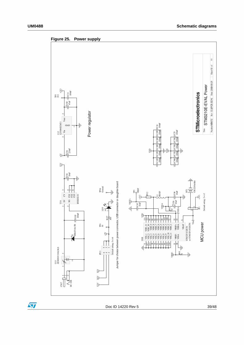
2.1 Power supplyThe STM3210E-EVAL evaluation board is designed to be powered by 5V DC power supply and to be protected by PolyZen U15 in the event of wrong power plug-in. It is possible to configure the evaluation board to use any of following three sources for the power supply:
● 5V DC power adapter connected to CN17, the power jack on the board (PSU on silk screen for power supply unit).
● 5V DC power with 500 mA limitation from CN14, the type-B USB connector (USB on silkscreen).
● 5V DC power from both CN10 and CN11, the extension connector for daughterboard (DTB for daughterboard on silkscreen).
The power supply is configured by setting the related jumpers JP13, JP12 and JP1 as described in Table 1. The LED LD5 is lit when the STM3210E-EVAL evaluation board is powered correctly.
Table 1. Power related jumpers
Jumper Description
JP13
JP13 is used to select one of the three possible power supply resources.For power supply jack(CN17) to the STM3210E-EVAL only, JP13 is set as shown (default setting).
For power supply from the daughterboard connectors(CN10 and CN11) to STM3210E-EVAL only, JP13 is set as shown.
For power supply from USB (CN14) to STM3210E-EVAL only, JP13 is set as shown.
For power supply from power supply jack(CN17) to both STM3210E-EVAL and daughterboard connected on CN10 and CN11, JP13 is set as shown (daughterboard must not have its own power supply connected).
JP12Enables consumption measurements of both VDD and VDDA.
Default setting: Fitted
JP1
Vbat is connected to 3.3V power when JP1 is set as shown (default setting).
Vbat is connected to battery when JP1 is set as shown.
PSU
DTB
U
SB
PS
U
DTB
U
SB
PSU
D
TB
US
B
PSU
DTB
USB
1 2 3
1 2 3
Hardware layout and configuration UM0488
8/48 Doc ID 14220 Rev 5
2.2 Boot optionThe STM3210E-EVAL evaluation board can boot from:
● Embedded user Flash
● System memory with boot loader for ISP
● Embedded SRAM for debugging
The boot option is configured by setting the switches BOOT0 and BOOT1.
2.3 Clock sourceTwo clock sources are available on the STM3210E-EVAL evaluation board for STM32F103 and RTC.
● X2, 32KHz crystal for embedded RTC.
● X1, 8MHz crystal with socket for STM32F103ZGT6 microcontroller, it can be removed from socket when internal RC clock is used.
2.4 Reset sourceThe reset signal of the STM3210E-EVAL evaluation board is low active and the reset sources include:
● Reset button B1
● Debugging tools from JTAG connector CN7 and trace connector CN9
● Daughterboard from CN11
Table 2. Boot related switches
Switch Boot fromSwitch
configuration
BOOT0BOOT1
STM3210E-EVAL boots from User Flash when BOOT0 is set as shown to the right. BOOT1 is not required in this configuration.
(Default setting)
STM3210E-EVAL boot from Embedded SRAM when BOOT0 and BOOT1 are set as shown to the right.
STM3210E-EVAL boot from System Memory when BOOT0 and BOOT1 are set as shown to the right.
0 < > 1
Boot 0
0 < > 1
Boot 0
Boot 1
0 < > 1
Boot 0
Boot 1
Table 3. Reset related jumper
Jumper Description
JP19Enables reset of the STM32F103ZGT6 embedded JTAG TAP controller each time a system reset occurs. JP19 connects the TRST signal from the JTAG connection with the system reset signal RESET#. Default setting: not fitted
UM0488 Hardware layout and configuration
Doc ID 14220 Rev 5 9/48
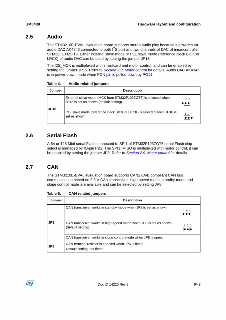
2.5 AudioThe STM3210E-EVAL evaluation board supports stereo audio play because it provides an audio DAC AK4343 connected to both I2S port and two channels of DAC of microcontroller STM32F103ZGT6. Either external slave mode or PLL slave mode (reference clock BICK or LRCK) of audio DAC can be used by setting the jumper JP18.
The I2S_MCK is multiplexed with smartcard and motor control, and can be enabled by setting the jumper JP15. Refer to Section 2.9: Motor control for details. Audio DAC AK4343 is in power-down mode when PDN pin is pulled-down by PG11.
2.6 Serial FlashA 64 or 128 Mbit serial Flash connected to SPI1 of STM32F103ZGT6 serial Flash chip select is managed by IO-pin PB2. The SPI1_MISO is multiplexed with motor control, it can be enabled by setting the jumper JP3. Refer to Section 2.9: Motor control for details.
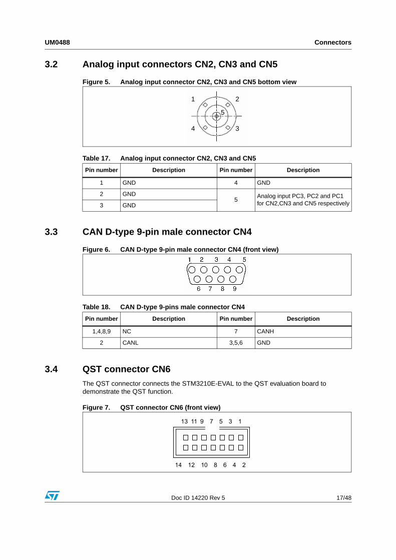
2.7 CANThe STM3210E-EVAL evaluation board supports CAN2.0A/B compliant CAN bus communication based on 3.3 V CAN transceiver. High-speed mode, standby mode and slope control mode are available and can be selected by setting JP8.
Table 4. Audio related jumpers
Jumper Description
JP18
External slave mode (MCK from STM32F103ZGT6) is selected when JP18 is set as shown (default setting).
PLL slave mode (reference clock BICK or LRCK) is selected when JP18 is set as shown.
1 2 3
1 2 3
Table 5. CAN related jumpers
Jumper Description
JP8
CAN transceiver works in standby mode when JP8 is set as shown.
CAN transceiver works in high-speed mode when JP8 is set as shown (default setting).
CAN transceiver works in slope control mode when JP8 is open.
JP6CAN terminal resistor is enabled when JP6 is fitted.
Default setting: not fitted
1 2 3
1 2 3
Hardware layout and configuration UM0488
10/48 Doc ID 14220 Rev 5
2.8 RS-232 connectorsTwo D-type 9-pin connectors CN12 (USART1) and CN8 (USART2) are available on the STM3210E-EVAL evaluation board.
● USART1 connector is connected to RS-232 transceiver U7 .
● USART2 connector with RTS/CTS handshake signal support is connected to RS-232 transceiver U5. The USART2_CTS is multiplexed with motor control, it can be enabled by setting jumper JP4. Refer to Section 2.9: Motor control for details.
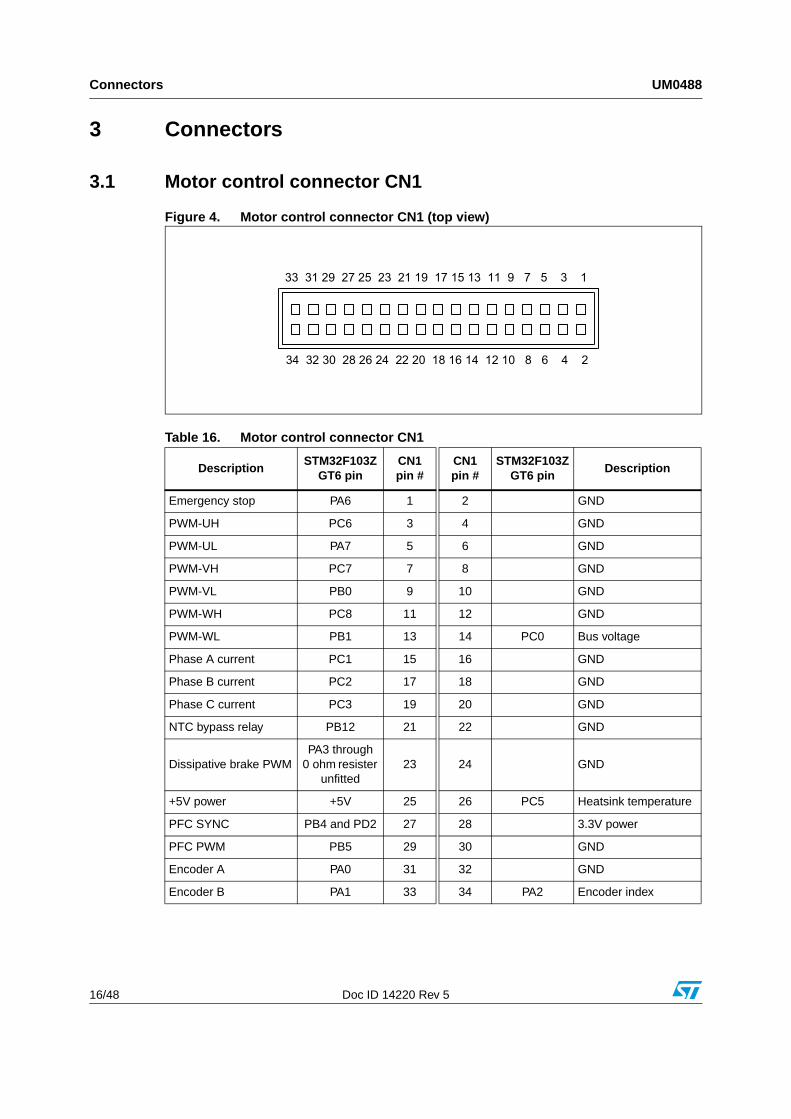
2.9 Motor controlThe STM3210E-EVAL evaluation board supports three-phase brushless motor control via a 34-pin connector CN1, which provides all required control and feedback signals to and from the motor power driving board. Available signals on this connector include emergency stop, motor speed, three-phase motor current, bus voltage, heatsink temperature from the motor driving board and 6 channels of PWM control signals going to the motor driving circuit.
JP 20 selects one of the two synchronization methods for power factor correction (PFC).
The I/O pins used on the motor control connector CN1 are multiplexed with some peripherals on the board; either the motor control connector or multiplexed peripherals can be enabled by setting the jumpers JP3, JP4, JP11, JP15 and JP16 as described in Table 6.
Table 6. Motor control related jumpers
Jumper DescriptionMultiplexed peripherals
JP20JP20 allows to have a PFC synchronization signal redirected to the timer 3 input capture 1 pin, and additionally to the timer 3 external trigger input. JTAG debugging is disabled when JP20 is fitted. Default setting: not fitted
JP2JP2 should be kept on open when encoder signal is input from pin 31 of CN1 while it should be kept on close when analog signal is from pin 31 of CN1 for special motor. Default setting: not fitted
JP4
MC_EnA is enabled when JP4 is set as shown to the right (default setting):
USART2_CTS is enabled when JP4 is set as show to the right:
USART2
JP3MC_EmergencySTOP is enabled when JP3 is closed. The pin PA6 is used as SPI1_MISO when JP3 is open. Default setting: not fitted
SPI1
JP11MC_PFCpwm is enabled when JP11 is open. The pin PB5 will be used as interrupt input from temperature sensor when JP11 is closed.
Temperature sensor
JP15MC_UH or I2S_MCK are enabled when JP15 is open. The pin PC6 is used as Smartcard_CMDVCC when JP15 is closed.
I2S and smartcard
JP16MC_VH is enabled when JP16 is open. The pin PC7 is used as Smartcard_OFF when JP16 is closed
Smartcard
1 2 3
1 2 3
UM0488 Hardware layout and configuration
Doc ID 14220 Rev 5 11/48
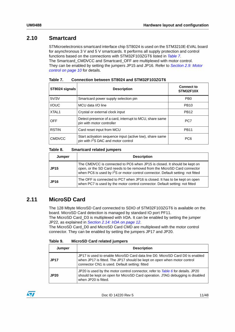
2.10 SmartcardSTMicroelectronics smartcard interface chip ST8024 is used on the STM3210E-EVAL board for asynchronous 3 V and 5 V smartcards. It performs all supply protection and control functions based on the connections with STM32F103ZGT6 listed in Table 7. The Smartcard_CMDVCC and Smartcard_OFF are multiplexed with motor control. They can be enabled by setting the jumpers JP15 and JP16. Refer to Section 2.9: Motor control on page 10 for details.
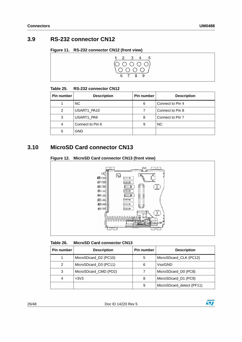
2.11 MicroSD CardThe 128 Mbyte MicroSD Card connected to SDIO of STM32F103ZGT6 is available on the board. MicroSD Card detection is managed by standard IO port PF11. The MicroSD Card_D3 is multiplexed with IrDA. It can be enabled by setting the jumper JP22, as explained in Section 2.14: IrDA on page 12.The MicroSD Card_D0 and MicroSD Card CMD are multiplexed with the motor control connector. They can be enabled by setting the jumpers JP17 and JP20.
Table 7. Connection between ST8024 and STM32F103ZGT6
ST8024 signals DescriptionConnect to STM32F10X
5V/3V Smartcard power supply selection pin PB0
I/OUC MCU data I/O line PB10
XTAL1 Crystal or external clock input PB12
OFFDetect presence of a card, interrupt to MCU, share same pin with motor controller
PC7
RSTIN Card reset input from MCU PB11
CMDVCCStart activation sequence input (active low), share same pin with I2S DAC and motor control
PC6
Table 8. Smartcard related jumpers
Jumper Description
JP15The CMDVCC is connected to PC6 when JP15 is closed. It should be kept on open, or the SD Card needs to be removed from the MicroSD Card connector when PC6 is used by I2S or motor control connector. Default setting: not fitted
JP16The OFF is connected to PC7 when JP16 is closed. It has to be kept on open when PC7 is used by the motor control connector. Default setting: not fitted
Table 9. MicroSD Card related jumpers
Jumper Description
JP17JP17 is used to enable MicroSD Card data line D0. MicroSD Card D0 is enabled when JP17 is fitted. The JP17 should be kept on open when motor control connector CN1 is used. Default setting: fitted
JP20JP20 is used by the motor control connector, refer to Table 6 for details. JP20 should be kept on open for MicroSD Card operation. JTAG debugging is disabled when JP20 is fitted.
Hardware layout and configuration UM0488
12/48 Doc ID 14220 Rev 5
2.12 Temperature sensorOne I2C interface temperature sensor STLM75 (–55°C to +125°C) connected to I2C of STM32F103ZGT6 is available on the board.
2.13 Analog inputThree BNC connectors CN2,CN3 and CN5 are connected to PC3, PC2 and PC1 of the STM32F103ZGT6 as external analog input. The 50 ohm terminal resistor can be enabled by closing the solder bridge JP23, JP24 and JP25 for each BNC connector. A low-pass filter can be implemented for each BNC connector CN5, CN3 and CN2 by replacing R5 and C22, R4 and C13, R3 and C9 with the right resistor and capacitor values, depending on the requirements of your application.
2.14 IrDAIrDA communication is supported by the IrDA transceiver U13 connected to USART3 of STM32F103ZGT6. The IrDA transceiver can be enabled or disabled by JP21.
2.15 USBThe STM3210E-EVAL evaluation board supports USB2.0 compliant full speed communication via a USB type B connector (CN14). The evaluation board can be powered by this USB connection at 5 V DC with a 500 mA current limitation. USB disconnection simulation can be implemented by disconnecting the 1.5 K pull-up resistor from USB+ line. The USB disconnection simulation feature is enabled by setting JP14.
Table 10. IrDA related jumpers
Jumper Description
JP21Enables/disables the IrDA transceiver. IrDA is enabled when JP21 is fitted (default setting).
IrDA is disabled when JP21 is not fitted.
JP22IrDA_RX is enabled when JP22 is closed.
I/O pin PC11 is data line 3 of the MicroSD Card when JP22 is open (default setting).
Table 11. USB related jumpers
Jumper Description
JP14
The USB 1.5K pull-up resistor is always connected to USB+ line when JP14 is set as shown.
The USB 1.5K pull-up resistor can be disconnected by software from USB+ line when JP14 is set as shown. In this case, the USB connect/disconnect feature is managed by standard IO port PB14 (default setting).
1 2 3
1 2 3
UM0488 Hardware layout and configuration
Doc ID 14220 Rev 5 13/48
2.16 Development and debug supportThe two debug connectors available on the STM3210E-EVAL evaluation board are:
● CN9: standard 20-pin JTAG interface connector, compliant with ARM7/9 debug tools.
● CN7: SAMTEC 20-pin connector FTSH-110-01-L-DV for both SWD and Trace, compliant with ARM CoreSight debug tools.
2.17 Display and input devicesThe 240x320 TFT color LCD connected to bank1 NOR/PSRAM4 of FSMC interface of the STM32F103ZGT6 and four general purpose color LEDs (LD 1,2,3,4) are available as display devices. A 4-direction joystick with selection key, general purpose button (B4), wakeup button (B2) and tamper detection button (B3) are available as input devices. The jumper JP4 should be kept open to enable the wakeup button B2 which shares the same I/O with USART2 and motor control connector.
The STM3210E-EVAL evaluation board also supports a second optional 122x32 graphic LCD that can be mounted on the U18 connector. By default, the graphic LCD is not present.
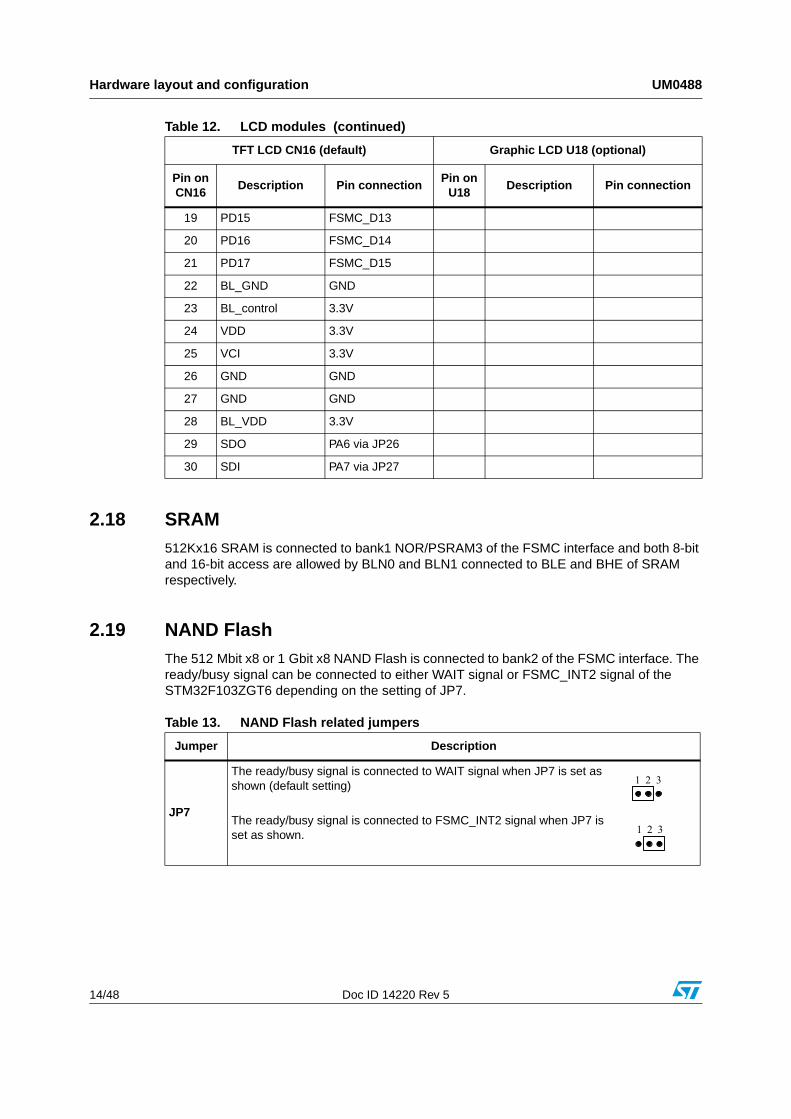
Table 12. LCD modules
TFT LCD CN16 (default) Graphic LCD U18 (optional)
Pin on CN16
Description Pin connectionPin on
U18Description Pin connection
1 CSCS of Bank3 of FSMC
1 Vss GND
2 RS FSMC_A0 2 Vcc 3.3V
3 WR/SCL FSMC_NWE 3 VO -
4 RD FSMC_NOE 4 CLK PA5
5 RESET RESET# 5 SID PA7
6 PD1 FSMC_D0 6 CS PF10
7 PD2 FSMC_D1 7 A +5V
8 PD3 FSMC_D2 8 K GND
9 PD4 FSMC_D3
10 PD5 FSMC_D4
11 PD6 FSMC_D5
12 PD7 FSMC_D6
13 PD8 FSMC_D7
14 PD10 FSMC_D8
15 PD11 FSMC_D9
16 PD12 FSMC_D10
17 PD13 FSMC_D11
18 PD14 FSMC_D12
Hardware layout and configuration UM0488
14/48 Doc ID 14220 Rev 5
2.18 SRAM512Kx16 SRAM is connected to bank1 NOR/PSRAM3 of the FSMC interface and both 8-bit and 16-bit access are allowed by BLN0 and BLN1 connected to BLE and BHE of SRAM respectively.
2.19 NAND FlashThe 512 Mbit x8 or 1 Gbit x8 NAND Flash is connected to bank2 of the FSMC interface. The ready/busy signal can be connected to either WAIT signal or FSMC_INT2 signal of the STM32F103ZGT6 depending on the setting of JP7.
19 PD15 FSMC_D13
20 PD16 FSMC_D14
21 PD17 FSMC_D15
22 BL_GND GND
23 BL_control 3.3V
24 VDD 3.3V
25 VCI 3.3V
26 GND GND
27 GND GND
28 BL_VDD 3.3V
29 SDO PA6 via JP26
30 SDI PA7 via JP27
Table 12. LCD modules (continued)
TFT LCD CN16 (default) Graphic LCD U18 (optional)
Pin on CN16
Description Pin connectionPin on
U18Description Pin connection
Table 13. NAND Flash related jumpers
Jumper Description
JP7
The ready/busy signal is connected to WAIT signal when JP7 is set as shown (default setting)
The ready/busy signal is connected to FSMC_INT2 signal when JP7 is set as shown.
1 2 3
1 2 3
UM0488 Hardware layout and configuration
Doc ID 14220 Rev 5 15/48
2.20 NOR Flash128 Mbit NOR Flash is connected to bank1 NOR/PSRAM2 of the FSMC interface. The 16-bit operation mode is selected by a pull-up resistor connected to the BYTE pin of the NOR Flash. Write protection can be enabled or disabled by jumper JP5.
Three different NOR 128-Mbit references can be present on the evaluation board depending on component availability.
These three references are not identical in terms of ID code, speed, timing or block protection. The demonstration firmware and the software library delivered with the board support these three NOR Flash references. However, during the development of your application software, you must verify which NOR reference is implemented on your board (component referenced as U2 on silkscreen and schematic), and take its characteristics into account.
Table 14. NOR Flash related jumpers
Jumper Description
JP5Write protection is enabled when JP5 is fitted.Write protection is disabled when JP5 is not fitted (default setting).
Table 15. NOR Flash reference
Reference Manufacturer
M29W128GL70ZA6E NUMONYX
M29W128GH70ZA6E NUMONYX
S29GL128P90FFIR20 SPANSION
Connectors UM0488
16/48 Doc ID 14220 Rev 5
3 Connectors
3.1 Motor control connector CN1
Figure 4. Motor control connector CN1 (top view)
Table 16. Motor control connector CN1
DescriptionSTM32F103Z
GT6 pinCN1 pin #
CN1 pin #
STM32F103ZGT6 pin
Description
Emergency stop PA6 1 2 GND
PWM-UH PC6 3 4 GND
PWM-UL PA7 5 6 GND
PWM-VH PC7 7 8 GND
PWM-VL PB0 9 10 GND
PWM-WH PC8 11 12 GND
PWM-WL PB1 13 14 PC0 Bus voltage
Phase A current PC1 15 16 GND
Phase B current PC2 17 18 GND
Phase C current PC3 19 20 GND
NTC bypass relay PB12 21 22 GND
Dissipative brake PWMPA3 through
0 ohm resister unfitted
23 24 GND
+5V power +5V 25 26 PC5 Heatsink temperature
PFC SYNC PB4 and PD2 27 28 3.3V power
PFC PWM PB5 29 30 GND
Encoder A PA0 31 32 GND
Encoder B PA1 33 34 PA2 Encoder index
33 31 29 27 25 23 21 19 17 15 13 11 9 7 5 3 1
34 32 30 28 26 24 22 20 18 16 14 12 10 8 6 4 2
UM0488 Connectors
Doc ID 14220 Rev 5 17/48
3.2 Analog input connectors CN2, CN3 and CN5
Figure 5. Analog input connector CN2, CN3 and CN5 bottom view
3.3 CAN D-type 9-pin male connector CN4
Figure 6. CAN D-type 9-pin male connector CN4 (front view)
3.4 QST connector CN6The QST connector connects the STM3210E-EVAL to the QST evaluation board to demonstrate the QST function.
Figure 7. QST connector CN6 (front view)
Table 17. Analog input connector CN2, CN3 and CN5
Pin number Description Pin number Description
1 GND 4 GND
2 GND5
Analog input PC3, PC2 and PC1 for CN2,CN3 and CN5 respectively3 GND
Table 21. RS-232 connector CN8 with RTS/CTS handshake support
Pin number Description Pin number Description
1 NC 6 Connect to Pin 4
2 USART2_PA3 7 USART2_PA1
3 USART2_PA2 8 USART2_PA0
4 Connect to Pin 6 9 NC
5 GND
Table 22. JTAG debugging connector CN9
Pin number Description Pin number Description
1 3.3V power 2 3.3V power
3 PB4 4 GND
5 PA15 6 GND
7 PA13 8 GND
9 PA14 10 GND
11 RTCK 12 GND
13 PB3 14 GND
15 RESET# 16 GND
17 DBGRQ 18 GND
19 DBGACK 20 GND
19 17 15 13 11 9 7 5 3 1
20 18 16 14 12 10 8 6 4 2
Connectors UM0488
20/48 Doc ID 14220 Rev 5
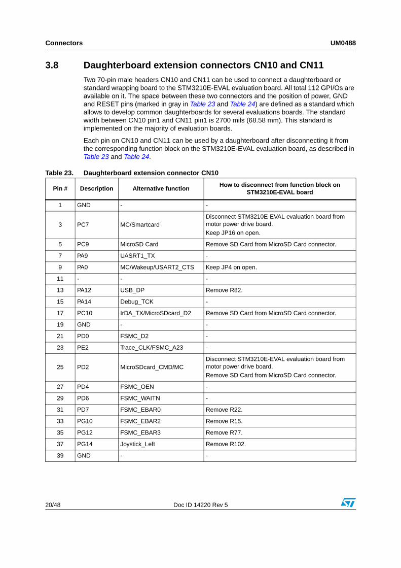
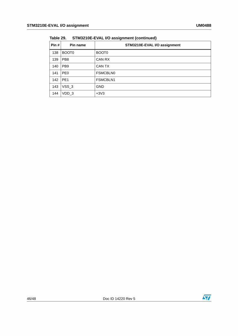
3.8 Daughterboard extension connectors CN10 and CN11Two 70-pin male headers CN10 and CN11 can be used to connect a daughterboard or standard wrapping board to the STM3210E-EVAL evaluation board. All total 112 GPI/Os are available on it. The space between these two connectors and the position of power, GND and RESET pins (marked in gray in Table 23 and Table 24) are defined as a standard which allows to develop common daughterboards for several evaluations boards. The standard width between CN10 pin1 and CN11 pin1 is 2700 mils (68.58 mm). This standard is implemented on the majority of evaluation boards.
Each pin on CN10 and CN11 can be used by a daughterboard after disconnecting it from the corresponding function block on the STM3210E-EVAL evaluation board, as described in Table 23 and Table 24.
Table 23. Daughterboard extension connector CN10
Pin # Description Alternative functionHow to disconnect from function block on
STM3210E-EVAL board
1 GND - -
3 PC7 MC/SmartcardDisconnect STM3210E-EVAL evaluation board from motor power drive board.
3.12 Audio jack CN15A 3.5 mm stereo audio jack CN15 connected to the audio DAC is available on the STM3210E-EVAL board.
3.13 TFT LCD connector CN16One 30-pin male header is available on the board to connect the LCD module board MB895 to the FSMC interface of the STM32F103ZGT6. Refer to Section 2.17: Display and input devices on page 13 for details.
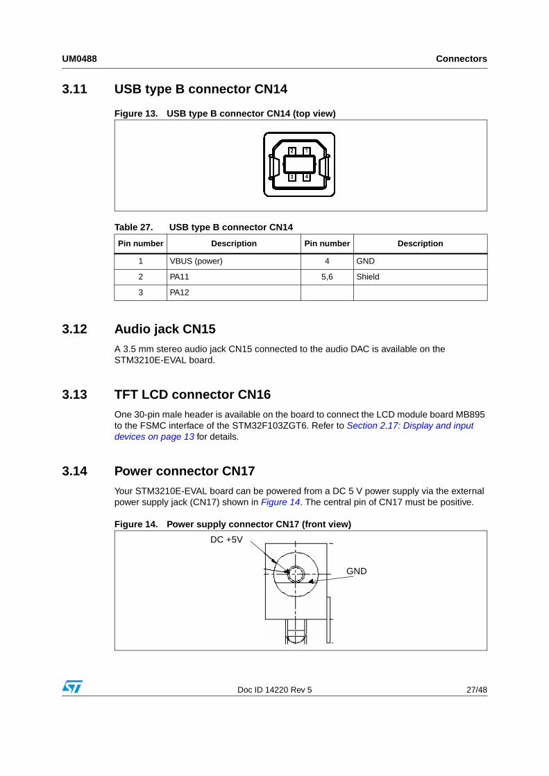
3.14 Power connector CN17Your STM3210E-EVAL board can be powered from a DC 5 V power supply via the external power supply jack (CN17) shown in Figure 14. The central pin of CN17 must be positive.
Figure 14. Power supply connector CN17 (front view)
Table 27. USB type B connector CN14
Pin number Description Pin number Description
1 VBUS (power) 4 GND
2 PA11 5,6 Shield
3 PA12
DC +5V
GND
Connectors UM0488
28/48 Doc ID 14220 Rev 5
3.15 Smartcard connector CN18
Figure 15. Smartcard connector CN18 (front view)
Table 28. Smartcard connector CN18
Pin number Description Pin number Description
1 VCC 5 GND
2 RST 6 NC
3 CLK 7 I/O
4 NC 8 NC
17 Detection pin of card presence 18 Detection pin of card presence
17 18
5 6 7 8
UM0488 Schematic diagrams
Doc ID 14220 Rev 5 29/48
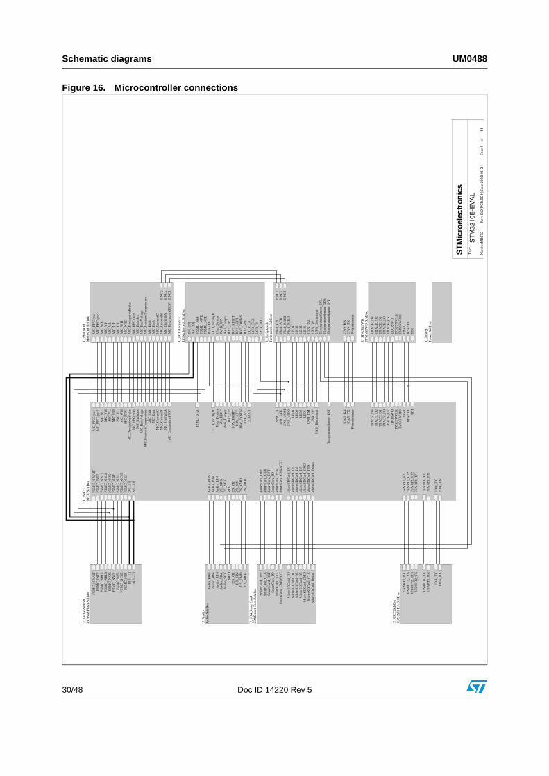
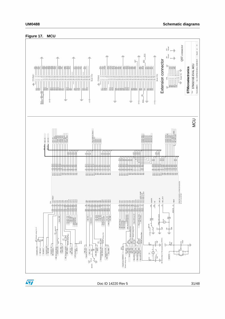
4 Schematic diagrams
This section provides the design schematics for the STM3210E-EVAL board key features, to help you implement these features in your applications. Schematics are provided for:
2-Jun-2008 2Added information on NOR Flash references in Section 2.20.Updated schematics in Section 4.
20-Nov-2008 3Modified cover page. Inserted a newChapter 1. Modified bank specified in Section 2.17, Section 2.18, Section 2.19 and Section 2.20.
21-Jan-2010 4Modified bank specified in Section 2.19.
Modified LCD in Section 3.13 and Figure 27.
01-Jul-2010 5Replaced STM32F103Z with STM32F103ZGT6.
64 KB internal SRAM and 512 KB Flash replaced with 96 KB internal SRAM and 1 MB Flash.
UM0488
48/48 Doc ID 14220 Rev 5
Please Read Carefully:
Information in this document is provided solely in connection with ST products. STMicroelectronics NV and its subsidiaries (“ST”) reserve theright to make changes, corrections, modifications or improvements, to this document, and the products and services described herein at anytime, without notice.
All ST products are sold pursuant to ST’s terms and conditions of sale.
Purchasers are solely responsible for the choice, selection and use of the ST products and services described herein, and ST assumes noliability whatsoever relating to the choice, selection or use of the ST products and services described herein.
No license, express or implied, by estoppel or otherwise, to any intellectual property rights is granted under this document. If any part of thisdocument refers to any third party products or services it shall not be deemed a license grant by ST for the use of such third party productsor services, or any intellectual property contained therein or considered as a warranty covering the use in any manner whatsoever of suchthird party products or services or any intellectual property contained therein.
UNLESS OTHERWISE SET FORTH IN ST’S TERMS AND CONDITIONS OF SALE ST DISCLAIMS ANY EXPRESS OR IMPLIEDWARRANTY WITH RESPECT TO THE USE AND/OR SALE OF ST PRODUCTS INCLUDING WITHOUT LIMITATION IMPLIEDWARRANTIES OF MERCHANTABILITY, FITNESS FOR A PARTICULAR PURPOSE (AND THEIR EQUIVALENTS UNDER THE LAWSOF ANY JURISDICTION), OR INFRINGEMENT OF ANY PATENT, COPYRIGHT OR OTHER INTELLECTUAL PROPERTY RIGHT.
UNLESS EXPRESSLY APPROVED IN WRITING BY AN AUTHORIZED ST REPRESENTATIVE, ST PRODUCTS ARE NOTRECOMMENDED, AUTHORIZED OR WARRANTED FOR USE IN MILITARY, AIR CRAFT, SPACE, LIFE SAVING, OR LIFE SUSTAININGAPPLICATIONS, NOR IN PRODUCTS OR SYSTEMS WHERE FAILURE OR MALFUNCTION MAY RESULT IN PERSONAL INJURY,DEATH, OR SEVERE PROPERTY OR ENVIRONMENTAL DAMAGE. ST PRODUCTS WHICH ARE NOT SPECIFIED AS "AUTOMOTIVEGRADE" MAY ONLY BE USED IN AUTOMOTIVE APPLICATIONS AT USER’S OWN RISK.
Resale of ST products with provisions different from the statements and/or technical features set forth in this document shall immediately voidany warranty granted by ST for the ST product or service described herein and shall not create or extend in any manner whatsoever, anyliability of ST.
ST and the ST logo are trademarks or registered trademarks of ST in various countries.
Information in this document supersedes and replaces all information previously supplied.
The ST logo is a registered trademark of STMicroelectronics. All other names are the property of their respective owners.
Australia - Belgium - Brazil - Canada - China - Czech Republic - Finland - France - Germany - Hong Kong - India - Israel - Italy - Japan - Malaysia - Malta - Morocco - Philippines - Singapore - Spain - Sweden - Switzerland - United Kingdom - United States of America