November 2015 DocID14798 Rev 9 1/72 UM0560 User manual STM8 bootloader Introduction This document describes the features and operation of the STM8 integrated bootloader program STSW-STM8068. This code embedded in the system memory of the device (ROM memory) allows memories, including Flash program memory, data EEPROM and RAM, to be written into the device using the standard serial interfaces LINUART/UART/USART, SPI and CAN. The bootloader code is similar for all STM8 versions. However, even though a peripheral may be present in a product, the product may not support it (for example the SPI is not supported in 128 Kbyte devices). In addition, different STM8 device types support different peripherals (see Table 5: Serial interfaces associated with STM8 devices for detailed information). For further information on the STM8 family features, pinout, electrical characteristics, mechanical data and ordering information, refer to the STM8 datasheets. Applicable microcontroller products are listed in the document. www.st.com
Transcript
November 2015 DocID14798 Rev 9 1/72
UM0560User manualSTM8 bootloader
Introduction
This document describes the features and operation of the STM8 integrated bootloader program STSW-STM8068. This code embedded in the system memory of the device (ROM memory) allows memories, including Flash program memory, data EEPROM and RAM, to be written into the device using the standard serial interfaces LINUART/UART/USART, SPI and CAN.
The bootloader code is similar for all STM8 versions. However, even though a peripheral may be present in a product, the product may not support it (for example the SPI is not supported in 128 Kbyte devices). In addition, different STM8 device types support different peripherals (see Table 5: Serial interfaces associated with STM8 devices for detailed information).
For further information on the STM8 family features, pinout, electrical characteristics, mechanical data and ordering information, refer to the STM8 datasheets.
Applicable microcontroller products are listed in the document.
The main task of the bootloader is to download the application program into the internal memories through the integrated peripherals (UARTs, SPI, or CAN) without using the SWIM protocol and dedicated hardware. Data are provided by any device (host) which is capable of sending information through one of the above-mentioned serial interfaces.
The bootloader permits downloading of application software into the device memories, including RAM, program and data memory, using standard serial interfaces. It is a complementary solution to programming via the SWIM debugging interface.
The bootloader code is stored in the internal boot ROM memory. After a reset, the bootloader code checks whether the program memory is virgin or whether a specific option byte is set allowing code modifications.
If these conditions are not fulfilled, the bootloader resumes and the user application is started.
In case of a successful check the bootloader is executed.
When the bootloader procedure starts, the main tasks are:
• Polling all supported serial interfaces to check which peripheral is used
• Programming code, data, option bytes and/or vector tables at the address(es) received from the host.
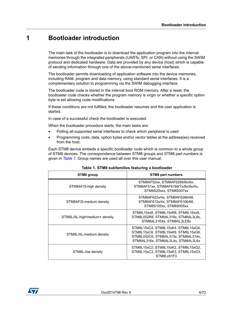
Each STM8 device embeds a specific bootloader code which is common to a whole group of STM8 devices. The correspondence between STM8 groups and STM8 part numbers is given in Table 1. Group names are used all over this user manual.
Table 2 gives the list of STM8 devices without embedded bootloader (no ROM bootloader is implemented inside the microcontroller). When using these devices, you have to write your own bootloader code and save it in the UBC program area (refer to STM8S, STM8AF, STM8L, STM8AL and STM8T family reference manuals for information on the UBC area).
1.1 Bootloader activation
The STM8 hardware reset vector is located at the beginning of the boot ROM (0x00 6000), while the other interrupt vectors are in the Flash program memory starting at address 0x00 8004.
The device executes the boot ROM (jumps inside the boot ROM area) and after checking certain address locations (see Table 4: Initial checking on page 10), it starts to execute the bootloader or the user code defined by the reset vector (0x00 8000).
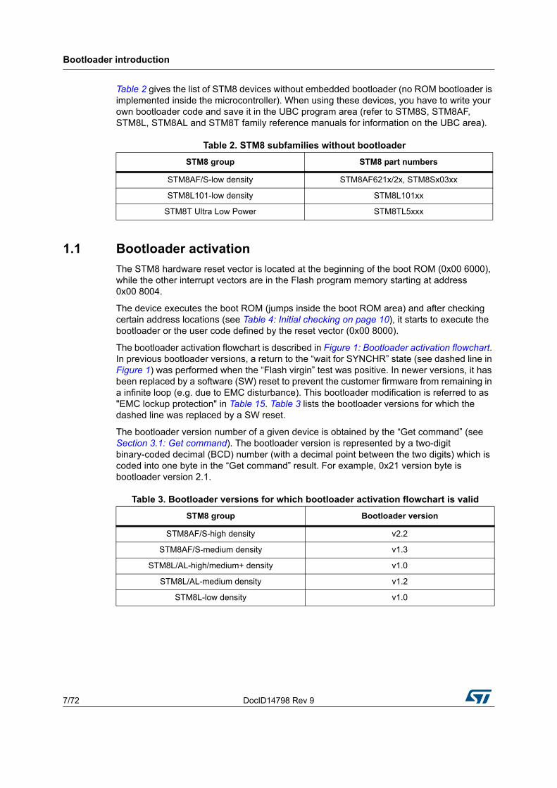
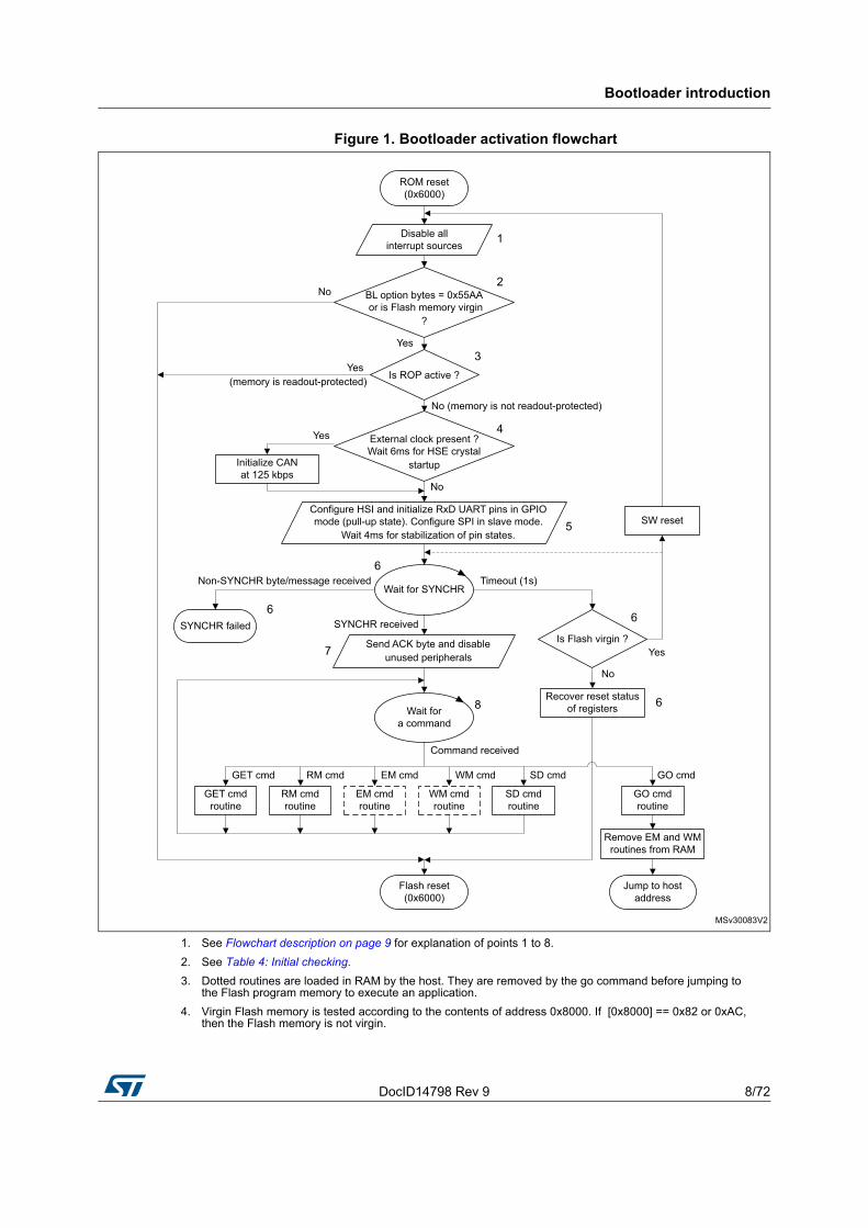
The bootloader activation flowchart is described in Figure 1: Bootloader activation flowchart. In previous bootloader versions, a return to the “wait for SYNCHR” state (see dashed line in Figure 1) was performed when the “Flash virgin” test was positive. In newer versions, it has been replaced by a software (SW) reset to prevent the customer firmware from remaining in a infinite loop (e.g. due to EMC disturbance). This bootloader modification is referred to as "EMC lockup protection" in Table 15. Table 3 lists the bootloader versions for which the dashed line was replaced by a SW reset.
The bootloader version number of a given device is obtained by the “Get command” (see Section 3.1: Get command). The bootloader version is represented by a two-digit binary-coded decimal (BCD) number (with a decimal point between the two digits) which is coded into one byte in the “Get command” result. For example, 0x21 version byte is bootloader version 2.1.
Table 2. STM8 subfamilies without bootloader
STM8 group STM8 part numbers
STM8AF/S-low density STM8AF621x/2x, STM8Sx03xx
STM8L101-low density STM8L101xx
STM8T Ultra Low Power STM8TL5xxx
Table 3. Bootloader versions for which bootloader activation flowchart is valid
STM8 group Bootloader version
STM8AF/S-high density v2.2
STM8AF/S-medium density v1.3
STM8L/AL-high/medium+ density v1.0
STM8L/AL-medium density v1.2
STM8L-low density v1.0
DocID14798 Rev 9 8/72
Bootloader introduction
71
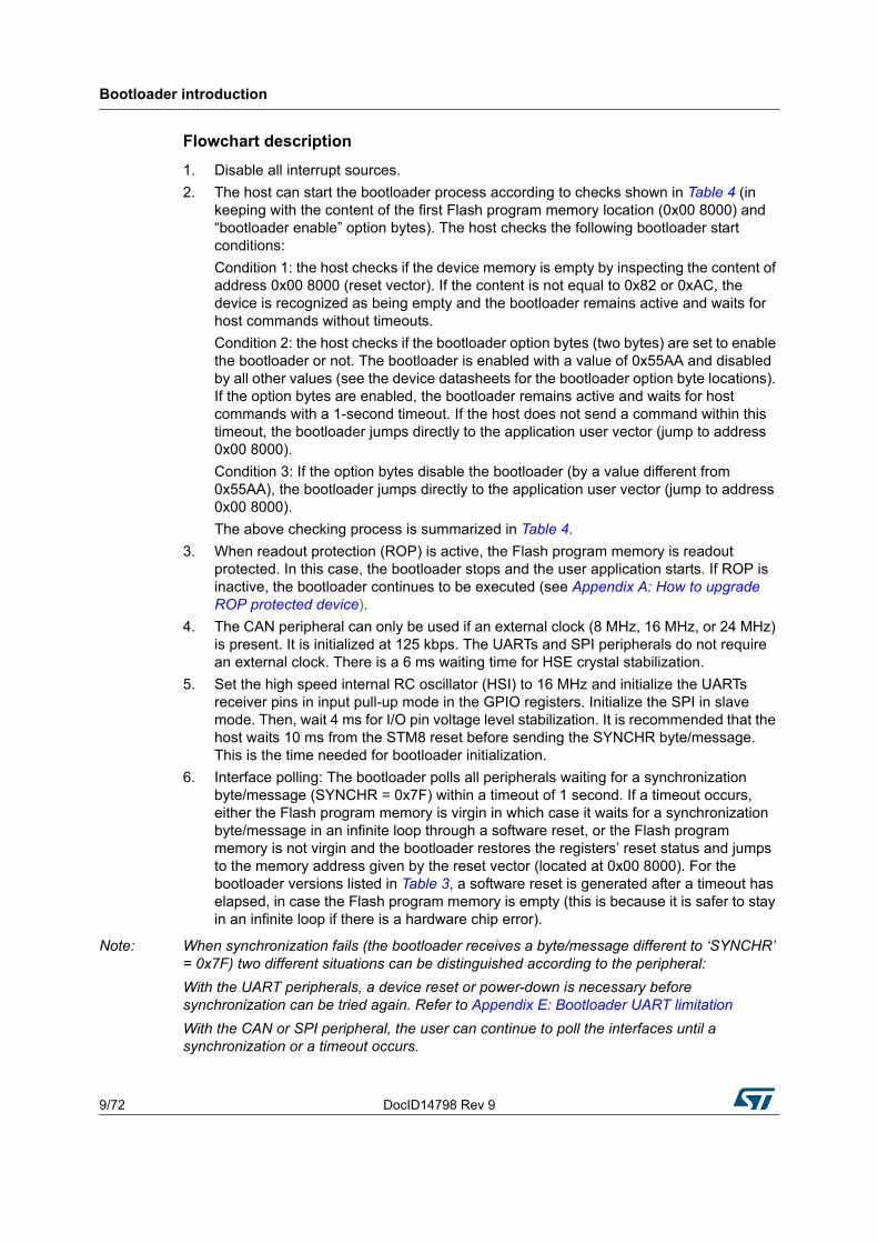
Figure 1. Bootloader activation flowchart
1. See Flowchart description on page 9 for explanation of points 1 to 8.
2. See Table 4: Initial checking.
3. Dotted routines are loaded in RAM by the host. They are removed by the go command before jumping to the Flash program memory to execute an application.
4. Virgin Flash memory is tested according to the contents of address 0x8000. If [0x8000] == 0x82 or 0xAC, then the Flash memory is not virgin.
Bootloader introduction
9/72 DocID14798 Rev 9
Flowchart description
1. Disable all interrupt sources.
2. The host can start the bootloader process according to checks shown in Table 4 (in keeping with the content of the first Flash program memory location (0x00 8000) and “bootloader enable” option bytes). The host checks the following bootloader start conditions:
Condition 1: the host checks if the device memory is empty by inspecting the content of address 0x00 8000 (reset vector). If the content is not equal to 0x82 or 0xAC, the device is recognized as being empty and the bootloader remains active and waits for host commands without timeouts.
Condition 2: the host checks if the bootloader option bytes (two bytes) are set to enable the bootloader or not. The bootloader is enabled with a value of 0x55AA and disabled by all other values (see the device datasheets for the bootloader option byte locations). If the option bytes are enabled, the bootloader remains active and waits for host commands with a 1-second timeout. If the host does not send a command within this timeout, the bootloader jumps directly to the application user vector (jump to address 0x00 8000).
Condition 3: If the option bytes disable the bootloader (by a value different from 0x55AA), the bootloader jumps directly to the application user vector (jump to address 0x00 8000).
The above checking process is summarized in Table 4.
3. When readout protection (ROP) is active, the Flash program memory is readout protected. In this case, the bootloader stops and the user application starts. If ROP is inactive, the bootloader continues to be executed (see Appendix A: How to upgrade ROP protected device).
4. The CAN peripheral can only be used if an external clock (8 MHz, 16 MHz, or 24 MHz) is present. It is initialized at 125 kbps. The UARTs and SPI peripherals do not require an external clock. There is a 6 ms waiting time for HSE crystal stabilization.
5. Set the high speed internal RC oscillator (HSI) to 16 MHz and initialize the UARTs receiver pins in input pull-up mode in the GPIO registers. Initialize the SPI in slave mode. Then, wait 4 ms for I/O pin voltage level stabilization. It is recommended that the host waits 10 ms from the STM8 reset before sending the SYNCHR byte/message. This is the time needed for bootloader initialization.
6. Interface polling: The bootloader polls all peripherals waiting for a synchronization byte/message (SYNCHR = 0x7F) within a timeout of 1 second. If a timeout occurs, either the Flash program memory is virgin in which case it waits for a synchronization byte/message in an infinite loop through a software reset, or the Flash program memory is not virgin and the bootloader restores the registers’ reset status and jumps to the memory address given by the reset vector (located at 0x00 8000). For the bootloader versions listed in Table 3, a software reset is generated after a timeout has elapsed, in case the Flash program memory is empty (this is because it is safer to stay in an infinite loop if there is a hardware chip error).
Note: When synchronization fails (the bootloader receives a byte/message different to ‘SYNCHR’ = 0x7F) two different situations can be distinguished according to the peripheral:
With the UART peripherals, a device reset or power-down is necessary before synchronization can be tried again. Refer to Appendix E: Bootloader UART limitation
With the CAN or SPI peripheral, the user can continue to poll the interfaces until a synchronization or a timeout occurs.
DocID14798 Rev 9 10/72
Bootloader introduction
71
7. If the synchronization message is received by the UARTs, the bootloader automatically detects the baud rate, initializes the UART and goes to step 8 below. If the synchronization message is received by the CAN or SPI, the bootloader goes directly to step 8 below.
Note: Once one of the available interfaces receives the synchronization message, all others are disabled.
8. Waiting for commands: Commands are checked in an infinite loop and executed. To exit from the bootloader, the host has to send a ‘GO’ command. When this is done, the bootloader removes the EM and WM routines from the RAM memory and jumps to the address selected by the host.
Note: To be able to write/erase data in Flash and EEPROM the host must write into RAM executable routines for writing and erasing. Those routines (*.s19 files) are provided with the bootloader. Host must upload those routines at address 0xA0. See section 3.8.1: RAM erase/write routines for more information.
Note: After interface initialization, the ROP bit is checked to avoid non-authorized reading of the Flash program memory and data EEPROM.
Table 4. Initial checking
Check order Condition checkedActual Flash program memory status
-> next action
1st [0x00 8000] <>(0x82 or 0xAC)
Flash program memory virgin. -> continue with bootloader
2nd [BL_OPT] == 0x55AA (1)
1. See device datasheet for the [BL_OPT] location in the option byte area memory map.
Flash program memory already written, bootloader enabled by option bytes.
-> continue with bootloader
3rd ROP (readout protection) is activeDevice protected by ROP.
-> jump to Flash program memory reset vector
Peripheral settings
11/72 DocID14798 Rev 9
2 Peripheral settings
This section describes the hardware settings of the STM8 communication peripherals:
• UARTs/LINUART
• SPI
• CAN
Note: During bootloading only one peripheral (first addressed) is enabled. All others are disabled.
2.1 USART/UARTs settings
This peripheral supports asynchronous serial communication. The USART/UARTs settings are:
• Data frame: 1 start bit, 8 data bit, 1 parity bit set to even, 1 stop bit
• Baud rate: The baud rate is automatically detected by the bootloader. When the user sends the synchronization byte, 0x7F, the bootloader automatically detects the baud rate and sets the USART/UARTs to the same baud rate. Maximum baud rate = 1 Mbps (115200 baud for STM8L/AL-high/medium+ density); minimum baud rate = 4800 bps.
To perform automatic speed detection, the RxD line must be stable in the application board (internal pull-up is enabled on the RxD line by the bootloader).
Pin settings:
• While bootloader is waiting for synchronization byte (SYNCH = 0x7F), RxD pins are set to input mode with pull-up.
• If bootloader is activated by USART/UART then TxD pins are set to push-pull mode.
• If bootloader is not activated (no SYNCH byte received within 1 second timeout) then all USART/UART pins are set to default reset state.
• If bootloader is activated by another interface (except USART/UART) then RxD pins remain in input mode with pull-up.
Table 5. Serial interfaces associated with STM8 devices(1)
1. The above table reflects only current bootloader versions and device states.
STM8 groups Serial interface
STM8AF-high density USART, LINUART (in “reply” mode), CAN
STM8AF-medium density LINUART (in “reply” mode), SPI
STM8S-high density UART1, UART3 (in “reply” mode), CAN
STM8S-medium density UART2 (in “reply” mode), SPI
STM8L-low density UART, SPI
STM8L/AL-medium density UART
STM8L/AL-high/medium+ densityUART1, UART2, UART3 (in “reply” mode), SPI1, SPI2
DocID14798 Rev 9 12/72
Peripheral settings
71
2.1.1 LINUART/UARTs in “reply” mode settings
Settings are:
• Data frame: 1 start bit, 8 data bit, no parity bit, 1 stop bit
• Baud rate: The baud rate is automatically detected by the bootloader. When the user sends the synchronization byte 0x7F, the bootloader automatically detects the baud rate and sets the UARTs to the same baud rate. Maximum baud rate = 550 kbps (115200 baud for STM8L/AL-high/medium+ density); minimum baud rate = 4800 bps.
To perform automatic speed detection, the RxD line must be stable in the application board (internal pull-up is enabled on the RxD line by the bootloader).
Reply mode
The host must reply to all the bytes sent from the bootloader. If TxD and RxD lines share the same physical medium (for example, 1-wire communication), then host replies are not necessary since RxD and TxD pins coincide.
Pin settings:
• While bootloader is waiting for synchronization byte (SYNCH = 0x7F), RxD pins are set to input mode with pull-up.
• If bootloader is activated by LINUART/UART then TxD pins are set to push-pull mode.
• If bootloader is not activated (no SYNCH byte received within 1 second timeout) then all LINUART/UART pins are set to default reset state.
• If bootloader is activated by another interface (except LINUART/UART) then RxD pins remain in input mode with pull-up.
2.2 SPI settings
The SPI settings are:
• 8 data bit, MSB first
• Bit rate: Set by the host which acts as a master
• Peripheral set in slave mode with software management of NSS
• Data polarity: CPOL = 0 (SCK to 0 when idle), CPHA = 0 (the first clock transition is the first data capture edge).
Before sending a ‘token’ byte, the host has to wait for a delay of a specified period of time. If this period is not quantified, it is equal to 6 µs.
The SPI peripheral is accessible via SPI_SCK, SPI_MOSI and SPI_MISO pins, with the following settings:
• While bootloader is waiting for synchronization byte (SYNCH = 0x7F) SPI_MISO pins are set to push-pull mode.
• If bootloader is not activated (no SYNCH byte received within 1 second timeout) then all SPI_MISO pins are set to default reset state.
• If bootloader is activated by another interface (except SPI) then SPI_MISO pins remain in push-pull mode.
Peripheral settings
13/72 DocID14798 Rev 9
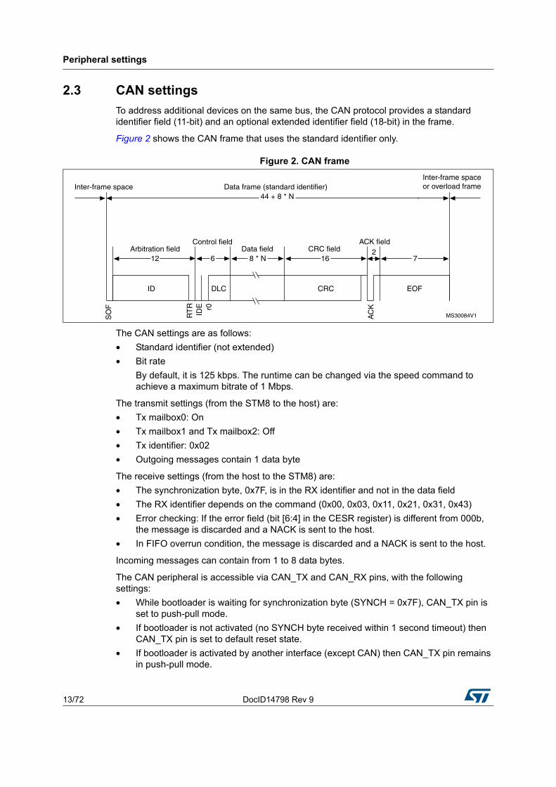
2.3 CAN settings
To address additional devices on the same bus, the CAN protocol provides a standard identifier field (11-bit) and an optional extended identifier field (18-bit) in the frame.
Figure 2 shows the CAN frame that uses the standard identifier only.
Figure 2. CAN frame
The CAN settings are as follows:
• Standard identifier (not extended)
• Bit rate
By default, it is 125 kbps. The runtime can be changed via the speed command to achieve a maximum bitrate of 1 Mbps.
The transmit settings (from the STM8 to the host) are:
• Tx mailbox0: On
• Tx mailbox1 and Tx mailbox2: Off
• Tx identifier: 0x02
• Outgoing messages contain 1 data byte
The receive settings (from the host to the STM8) are:
• The synchronization byte, 0x7F, is in the RX identifier and not in the data field
• The RX identifier depends on the command (0x00, 0x03, 0x11, 0x21, 0x31, 0x43)
• Error checking: If the error field (bit [6:4] in the CESR register) is different from 000b, the message is discarded and a NACK is sent to the host.
• In FIFO overrun condition, the message is discarded and a NACK is sent to the host.
Incoming messages can contain from 1 to 8 data bytes.
The CAN peripheral is accessible via CAN_TX and CAN_RX pins, with the following settings:
• While bootloader is waiting for synchronization byte (SYNCH = 0x7F), CAN_TX pin is set to push-pull mode.
• If bootloader is not activated (no SYNCH byte received within 1 second timeout) then CAN_TX pin is set to default reset state.
• If bootloader is activated by another interface (except CAN) then CAN_TX pin remains in push-pull mode.
DocID14798 Rev 9 14/72
Bootloader command set
71
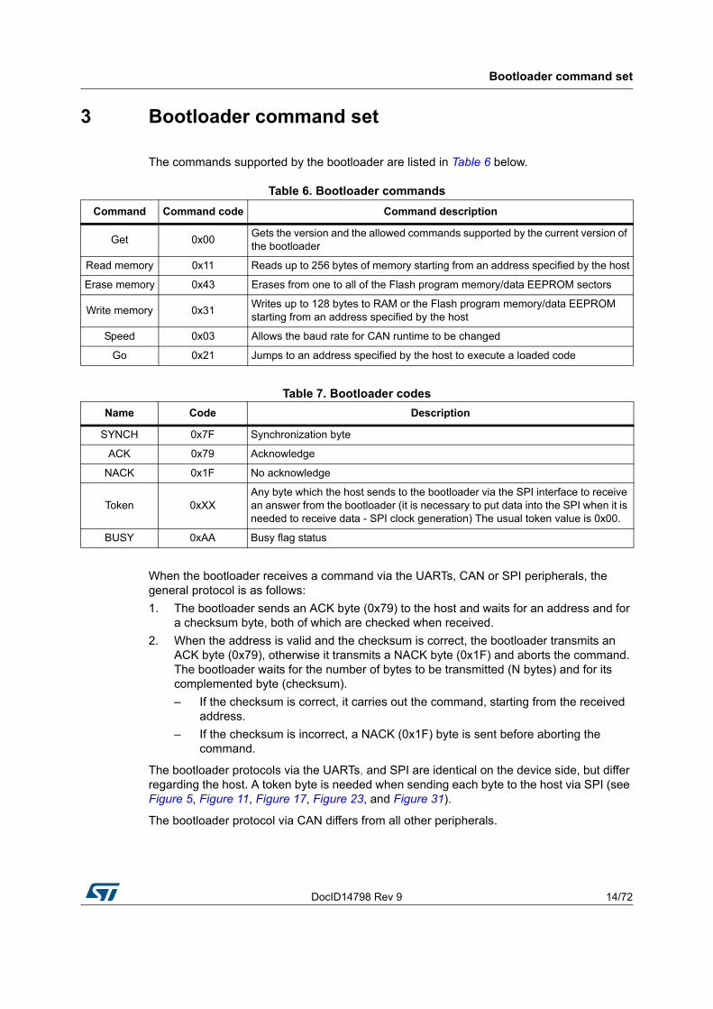
3 Bootloader command set
The commands supported by the bootloader are listed in Table 6 below.
Table 7. Bootloader codes
When the bootloader receives a command via the UARTs, CAN or SPI peripherals, the general protocol is as follows:
1. The bootloader sends an ACK byte (0x79) to the host and waits for an address and for a checksum byte, both of which are checked when received.
2. When the address is valid and the checksum is correct, the bootloader transmits an ACK byte (0x79), otherwise it transmits a NACK byte (0x1F) and aborts the command. The bootloader waits for the number of bytes to be transmitted (N bytes) and for its complemented byte (checksum).
– If the checksum is correct, it carries out the command, starting from the received address.
– If the checksum is incorrect, a NACK (0x1F) byte is sent before aborting the command.
The bootloader protocols via the UARTs, and SPI are identical on the device side, but differ regarding the host. A token byte is needed when sending each byte to the host via SPI (see Figure 5, Figure 11, Figure 17, Figure 23, and Figure 31).
The bootloader protocol via CAN differs from all other peripherals.
Table 6. Bootloader commands
Command Command code Command description
Get 0x00Gets the version and the allowed commands supported by the current version of the bootloader
Read memory 0x11 Reads up to 256 bytes of memory starting from an address specified by the host
Erase memory 0x43 Erases from one to all of the Flash program memory/data EEPROM sectors
Write memory 0x31Writes up to 128 bytes to RAM or the Flash program memory/data EEPROM starting from an address specified by the host
Speed 0x03 Allows the baud rate for CAN runtime to be changed
Go 0x21 Jumps to an address specified by the host to execute a loaded code
Name Code Description
SYNCH 0x7F Synchronization byte
ACK 0x79 Acknowledge
NACK 0x1F No acknowledge
Token 0xXXAny byte which the host sends to the bootloader via the SPI interface to receive an answer from the bootloader (it is necessary to put data into the SPI when it is needed to receive data - SPI clock generation) The usual token value is 0x00.
BUSY 0xAA Busy flag status
Bootloader command set
15/72 DocID14798 Rev 9
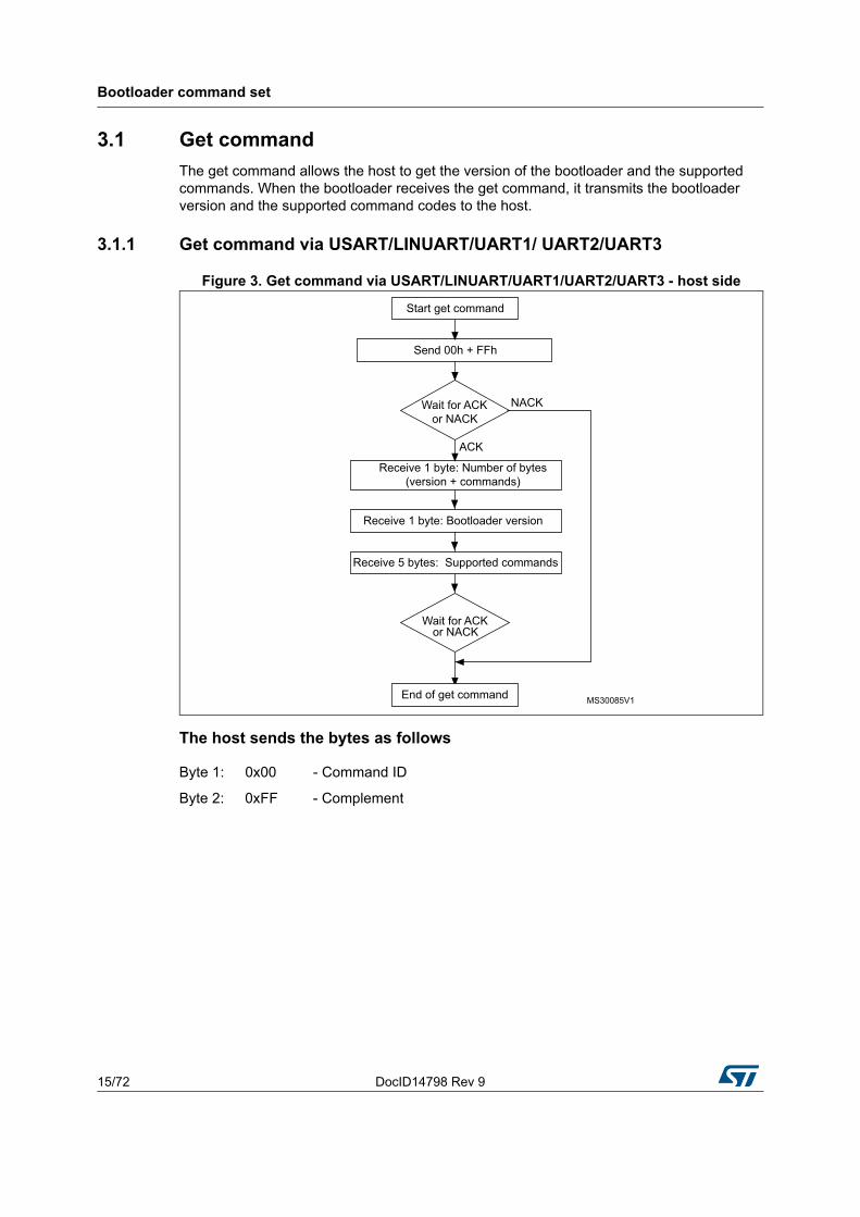
3.1 Get command
The get command allows the host to get the version of the bootloader and the supported commands. When the bootloader receives the get command, it transmits the bootloader version and the supported command codes to the host.
3.1.1 Get command via USART/LINUART/UART1/ UART2/UART3
Figure 3. Get command via USART/LINUART/UART1/UART2/UART3 - host side
The host sends the bytes as follows
Byte 1: 0x00 - Command ID
Byte 2: 0xFF - Complement
DocID14798 Rev 9 16/72
Bootloader command set
71
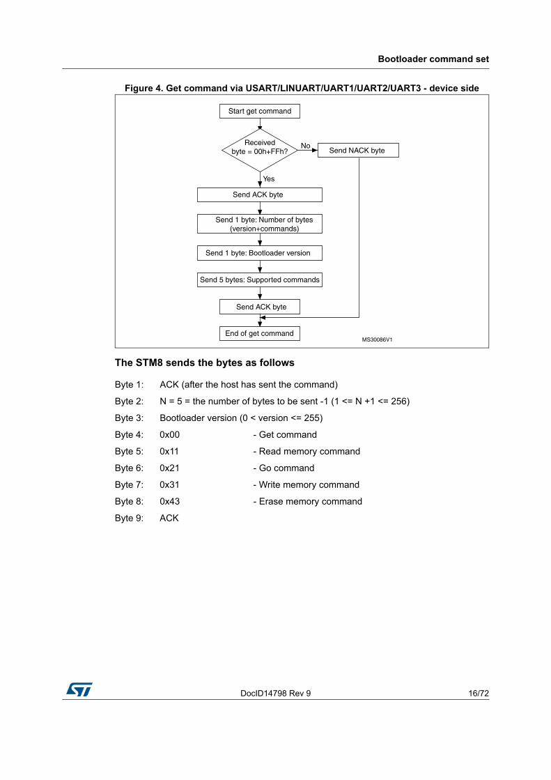
Figure 4. Get command via USART/LINUART/UART1/UART2/UART3 - device side
The STM8 sends the bytes as follows
Byte 1: ACK (after the host has sent the command)
Byte 2: N = 5 = the number of bytes to be sent -1 (1 <= N +1 <= 256)
Byte 3: Bootloader version (0 < version <= 255)
Byte 4: 0x00 - Get command
Byte 5: 0x11 - Read memory command
Byte 6: 0x21 - Go command
Byte 7: 0x31 - Write memory command
Byte 8: 0x43 - Erase memory command
Byte 9: ACK
Bootloader command set
17/72 DocID14798 Rev 9
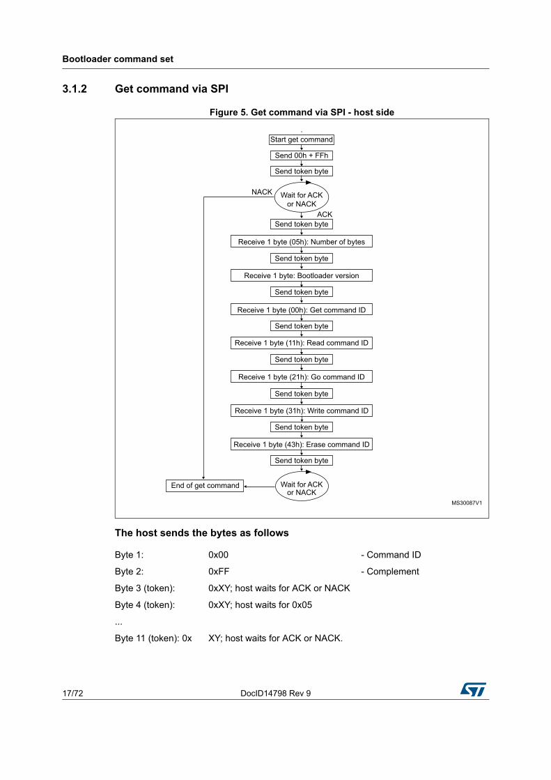
3.1.2 Get command via SPI
Figure 5. Get command via SPI - host side
The host sends the bytes as follows
Byte 1: 0x00 - Command ID
Byte 2: 0xFF - Complement
Byte 3 (token): 0xXY; host waits for ACK or NACK
Byte 4 (token): 0xXY; host waits for 0x05
...
Byte 11 (token): 0x XY; host waits for ACK or NACK.
DocID14798 Rev 9 18/72
Bootloader command set
71
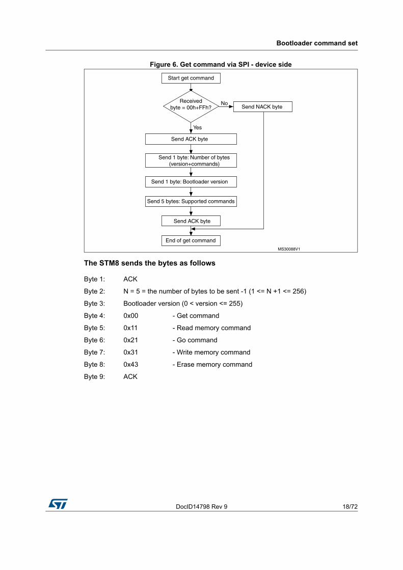
Figure 6. Get command via SPI - device side
The STM8 sends the bytes as follows
Byte 1: ACK
Byte 2: N = 5 = the number of bytes to be sent -1 (1 <= N +1 <= 256)
Byte 3: Bootloader version (0 < version <= 255)
Byte 4: 0x00 - Get command
Byte 5: 0x11 - Read memory command
Byte 6: 0x21 - Go command
Byte 7: 0x31 - Write memory command
Byte 8: 0x43 - Erase memory command
Byte 9: ACK
Bootloader command set
19/72 DocID14798 Rev 9
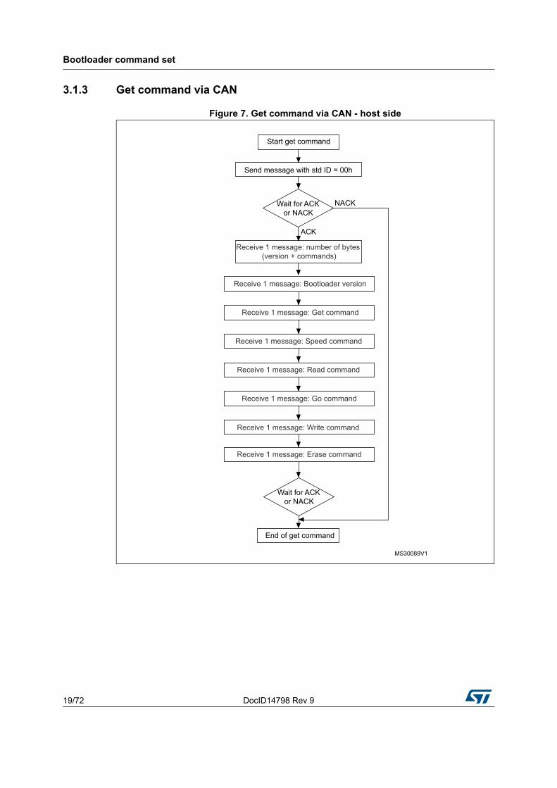
3.1.3 Get command via CAN
Figure 7. Get command via CAN - host side
DocID14798 Rev 9 20/72
Bootloader command set
71
The host sends the messages as follows
Command message: Std ID = 0x00, data length code (DLC) = ‘not important’.
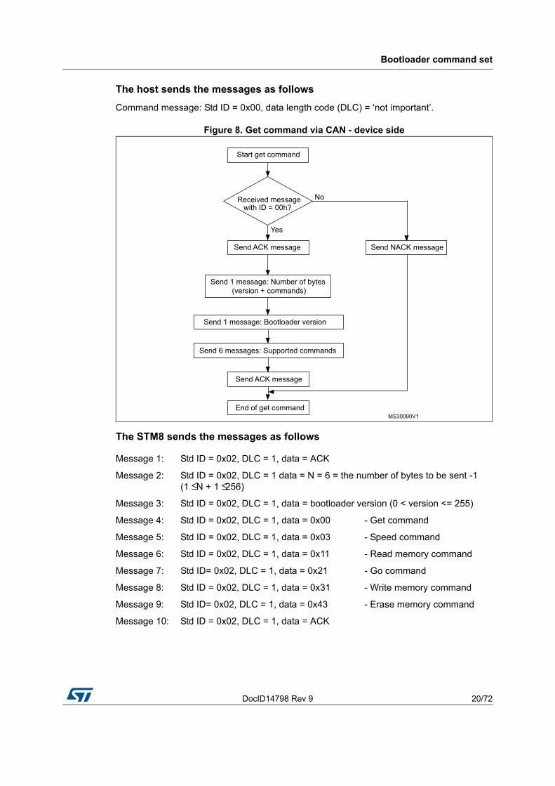
Figure 8. Get command via CAN - device side
The STM8 sends the messages as follows
Message 1: Std ID = 0x02, DLC = 1, data = ACK
Message 2: Std ID = 0x02, DLC = 1 data = N = 6 = the number of bytes to be sent -1 (1 ≤ N + 1 ≤ 256)
Message 3: Std ID = 0x02, DLC = 1, data = bootloader version (0 < version <= 255)
Message 4: Std ID = 0x02, DLC = 1, data = 0x00 - Get command
Message 5: Std ID = 0x02, DLC = 1, data = 0x03 - Speed command
Message 6: Std ID = 0x02, DLC = 1, data = 0x11 - Read memory command
Message 7: Std ID= 0x02, DLC = 1, data = 0x21 - Go command
Message 8: Std ID = 0x02, DLC = 1, data = 0x31 - Write memory command
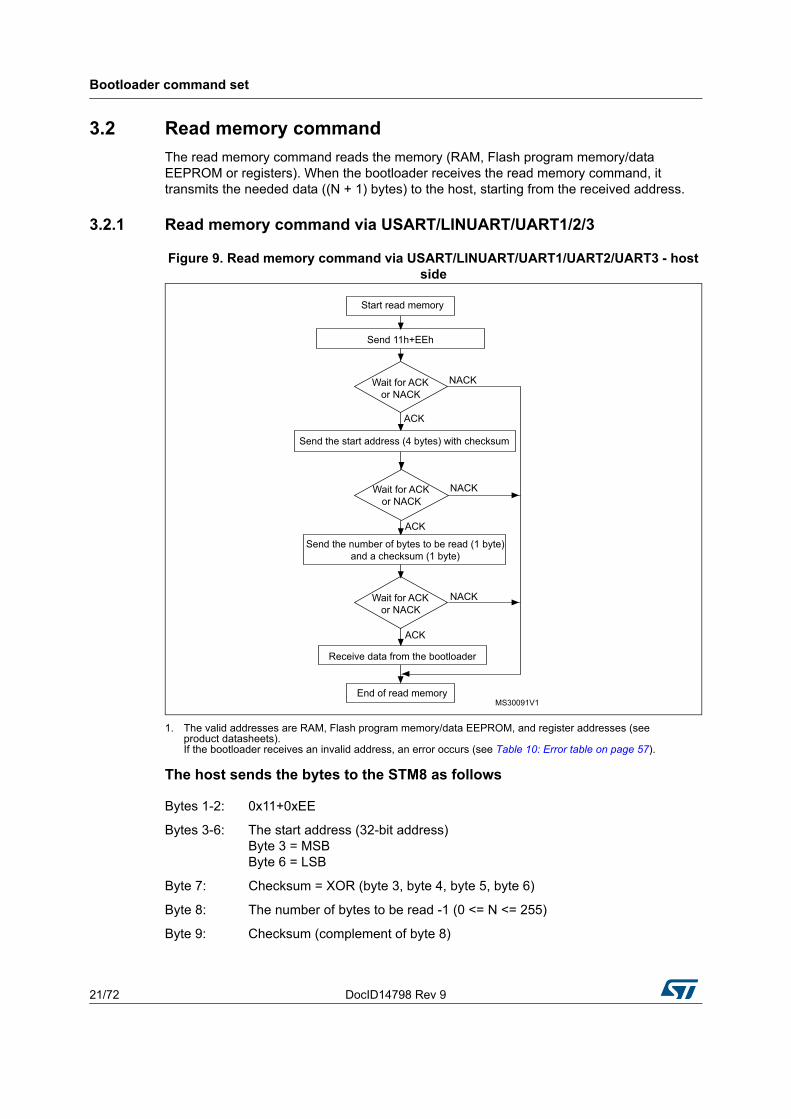
The read memory command reads the memory (RAM, Flash program memory/data EEPROM or registers). When the bootloader receives the read memory command, it transmits the needed data ((N + 1) bytes) to the host, starting from the received address.
3.2.1 Read memory command via USART/LINUART/UART1/2/3
Figure 9. Read memory command via USART/LINUART/UART1/UART2/UART3 - host side
1. The valid addresses are RAM, Flash program memory/data EEPROM, and register addresses (see product datasheets).If the bootloader receives an invalid address, an error occurs (see Table 10: Error table on page 57).
Byte 8: The number of bytes to be read -1 (0 <= N <= 255)
Byte 9: Checksum (complement of byte 8)
DocID14798 Rev 9 22/72
Bootloader command set
71
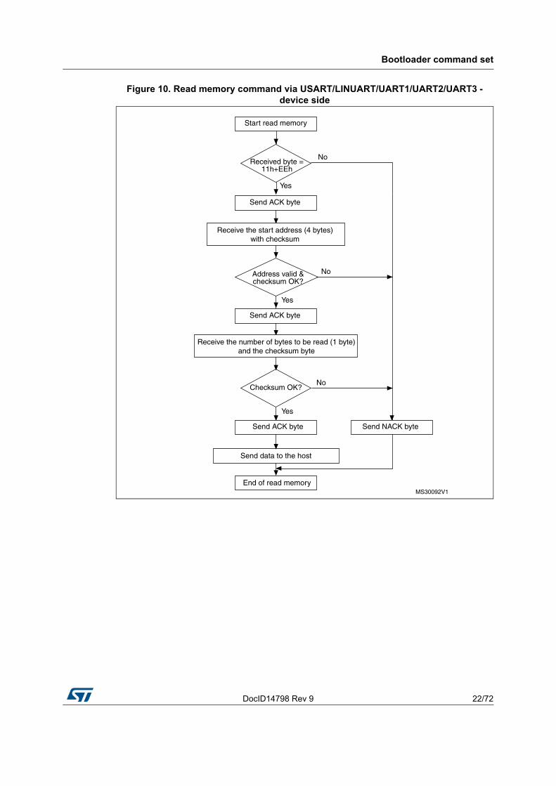
Figure 10. Read memory command via USART/LINUART/UART1/UART2/UART3 - device side
Bootloader command set
23/72 DocID14798 Rev 9
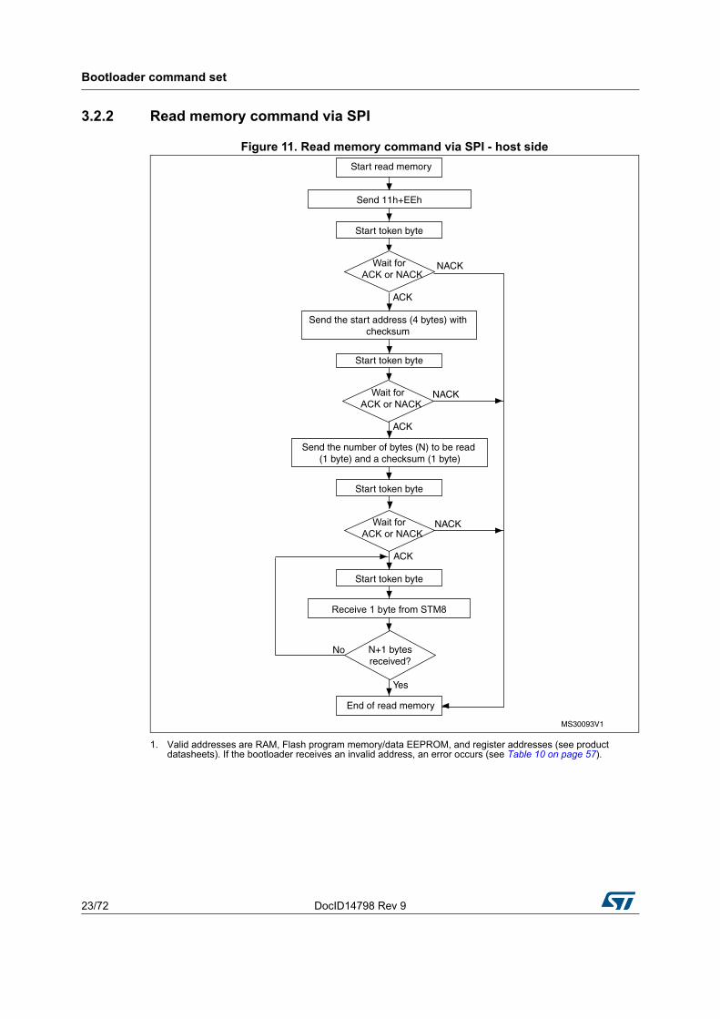
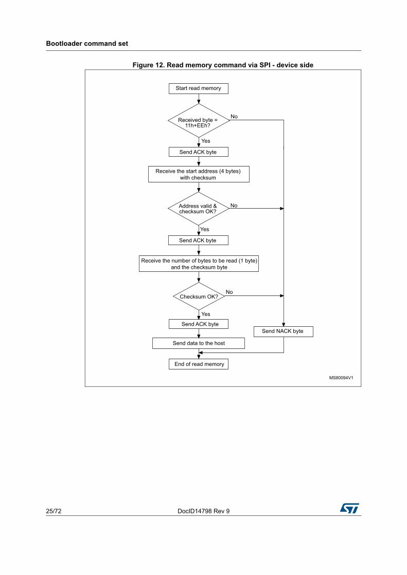
3.2.2 Read memory command via SPI
Figure 11. Read memory command via SPI - host side
1. Valid addresses are RAM, Flash program memory/data EEPROM, and register addresses (see product datasheets). If the bootloader receives an invalid address, an error occurs (see Table 10 on page 57).
DocID14798 Rev 9 24/72
Bootloader command set
71
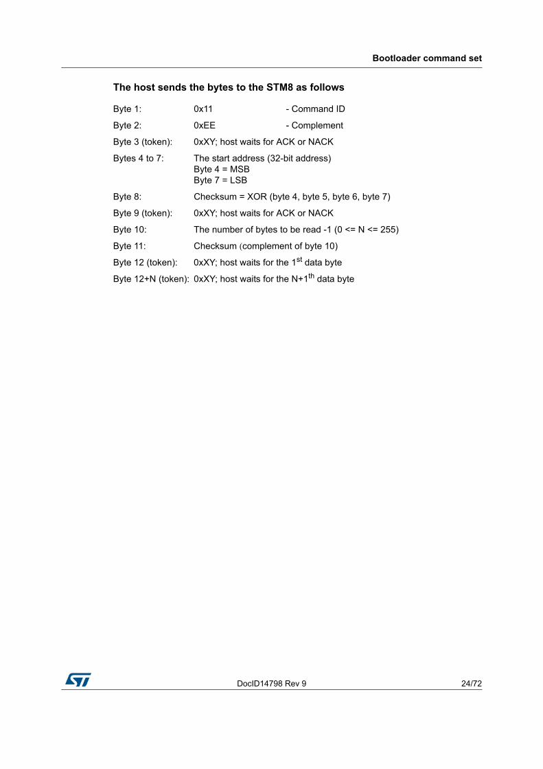
The host sends the bytes to the STM8 as follows
Byte 1: 0x11 - Command ID
Byte 2: 0xEE - Complement
Byte 3 (token): 0xXY; host waits for ACK or NACK
Bytes 4 to 7: The start address (32-bit address)Byte 4 = MSBByte 7 = LSB
Byte 10: The number of bytes to be read -1 (0 <= N <= 255)
Byte 11: Checksum (complement of byte 10)
Byte 12 (token): 0xXY; host waits for the 1st data byte
Byte 12+N (token): 0xXY; host waits for the N+1th data byte
Bootloader command set
25/72 DocID14798 Rev 9
Figure 12. Read memory command via SPI - device side
DocID14798 Rev 9 26/72
Bootloader command set
71
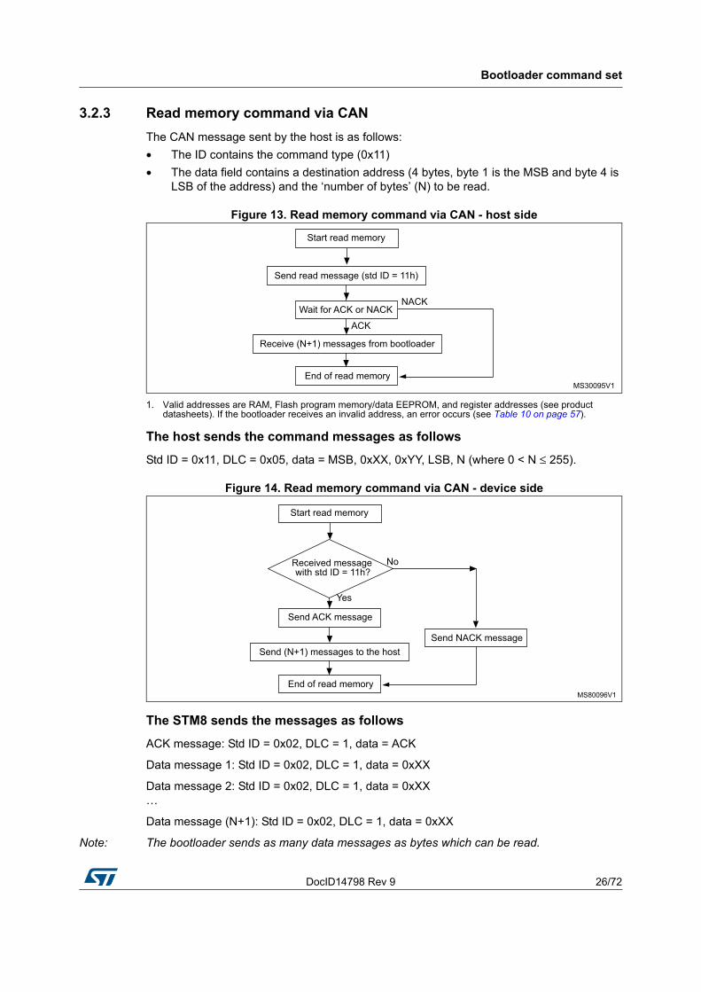
3.2.3 Read memory command via CAN
The CAN message sent by the host is as follows:
• The ID contains the command type (0x11)
• The data field contains a destination address (4 bytes, byte 1 is the MSB and byte 4 is LSB of the address) and the ‘number of bytes’ (N) to be read.
Figure 13. Read memory command via CAN - host side
1. Valid addresses are RAM, Flash program memory/data EEPROM, and register addresses (see product datasheets). If the bootloader receives an invalid address, an error occurs (see Table 10 on page 57).
The host sends the command messages as follows
Std ID = 0x11, DLC = 0x05, data = MSB, 0xXX, 0xYY, LSB, N (where 0 < N ≤ 255).
Figure 14. Read memory command via CAN - device side
The STM8 sends the messages as follows
ACK message: Std ID = 0x02, DLC = 1, data = ACK
Data message 1: Std ID = 0x02, DLC = 1, data = 0xXX
Data message 2: Std ID = 0x02, DLC = 1, data = 0xXX…
Data message (N+1): Std ID = 0x02, DLC = 1, data = 0xXX
Note: The bootloader sends as many data messages as bytes which can be read.
Bootloader command set
27/72 DocID14798 Rev 9
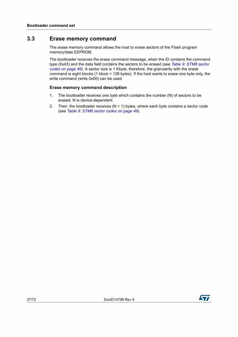
3.3 Erase memory command
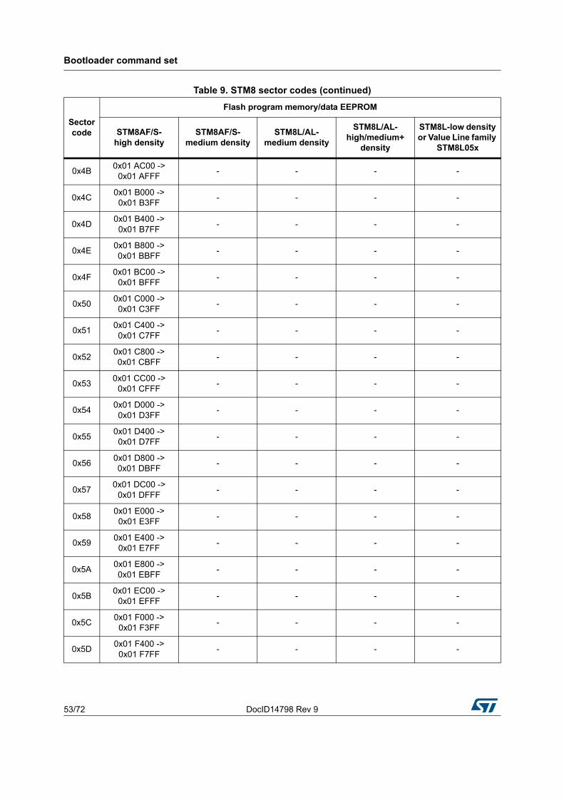
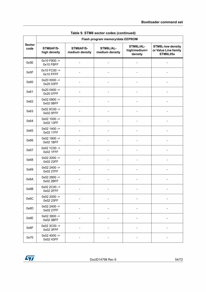
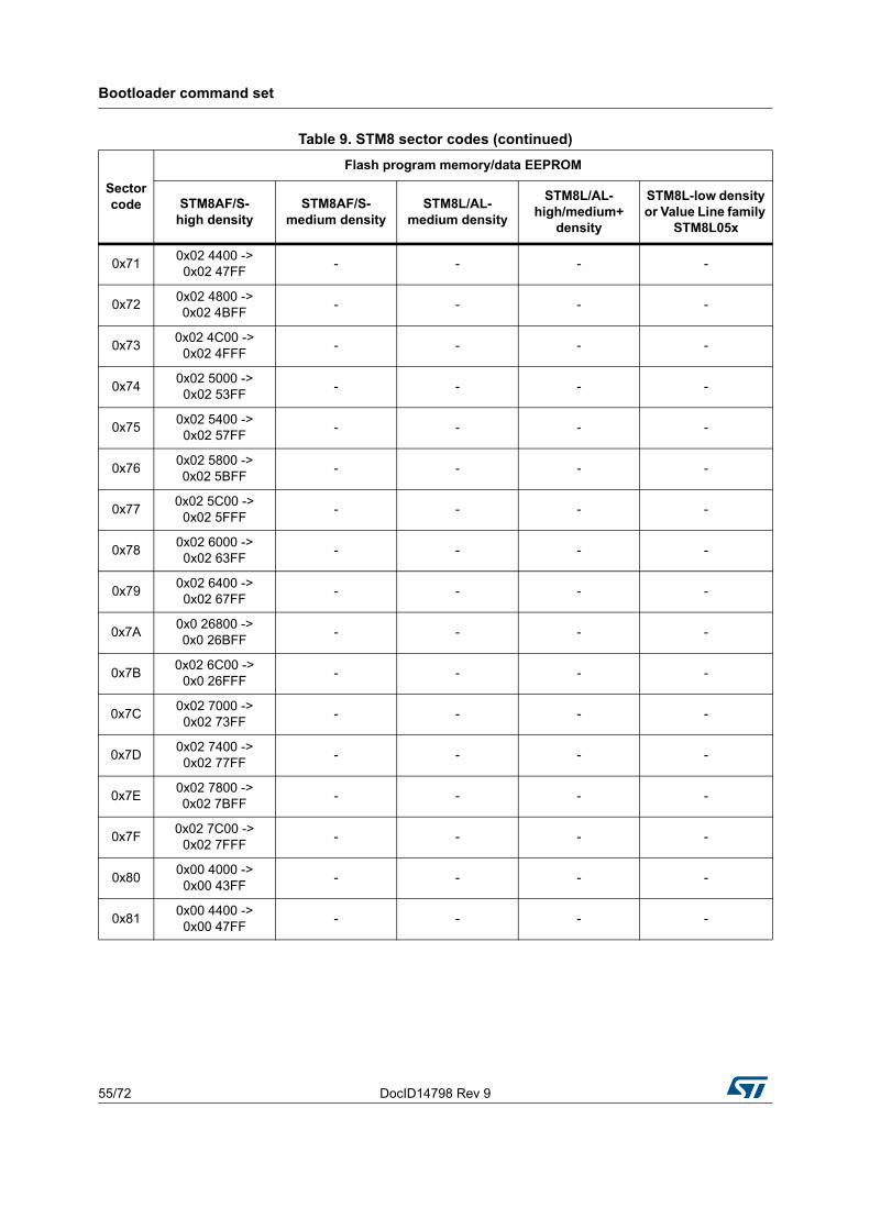
The erase memory command allows the host to erase sectors of the Flash program memory/data EEPROM.
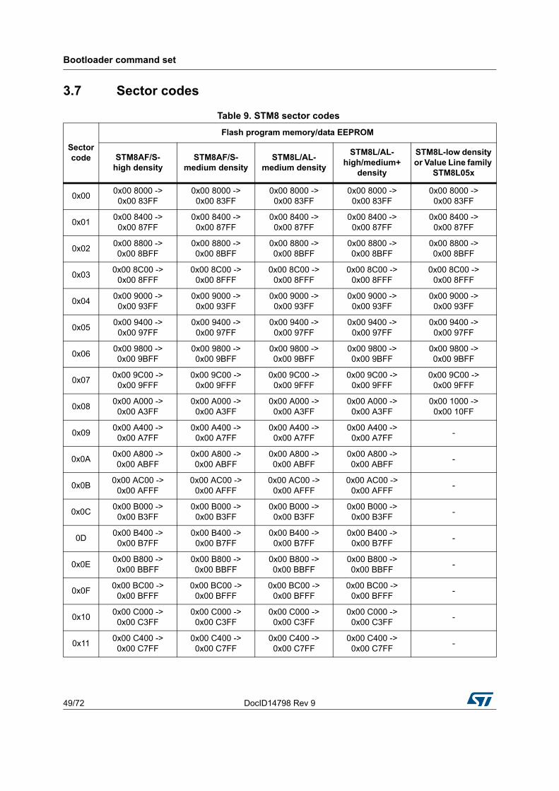
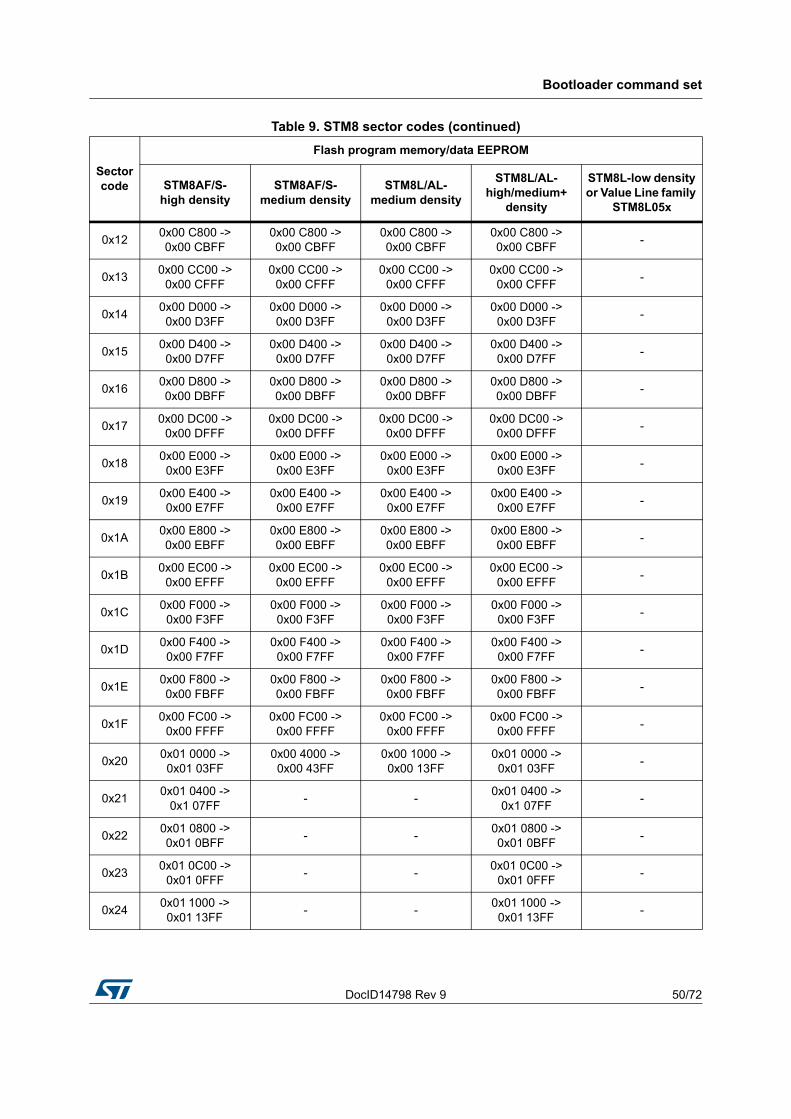
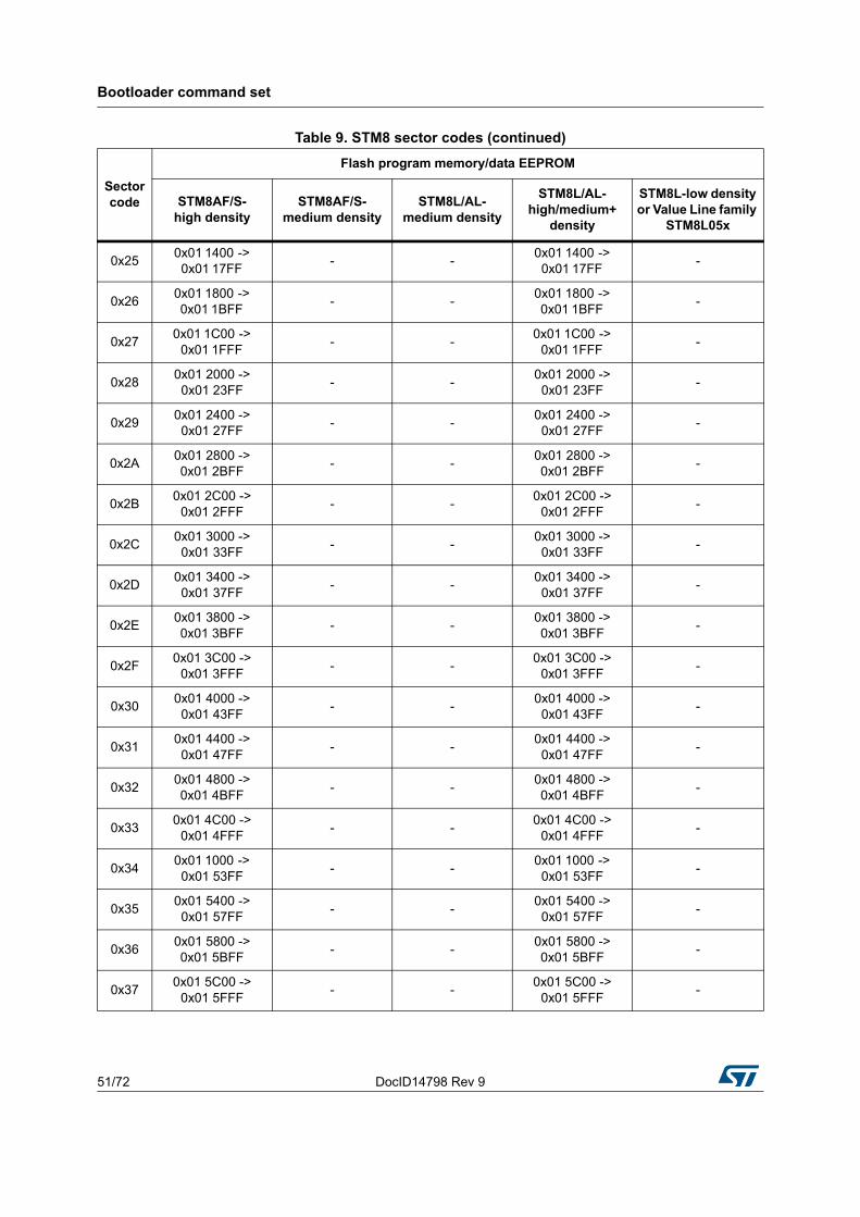
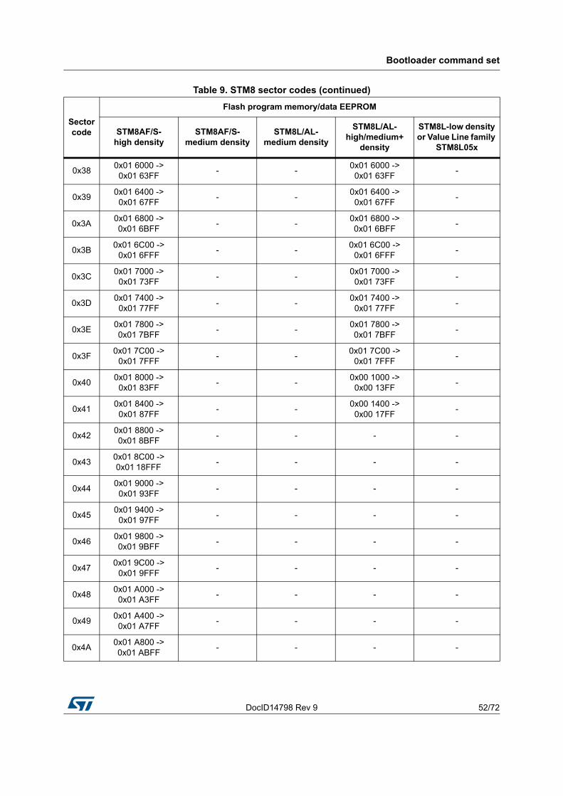
The bootloader receives the erase command message, when the ID contains the command type (0x43) and the data field contains the sectors to be erased (see Table 9: STM8 sector codes on page 49). A sector size is 1 Kbyte, therefore, the granularity with the erase command is eight blocks (1 block = 128 bytes). If the host wants to erase one byte only, the write command (write 0x00) can be used.
Erase memory command description
1. The bootloader receives one byte which contains the number (N) of sectors to be erased. N is device-dependent.
2. Then, the bootloader receives (N + 1) bytes, where each byte contains a sector code (see Table 9: STM8 sector codes on page 49).
DocID14798 Rev 9 28/72
Bootloader command set
71
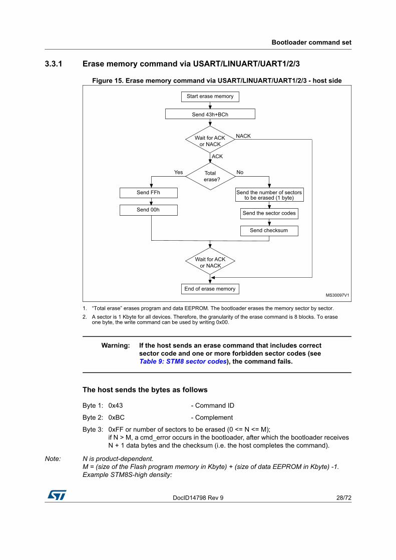
3.3.1 Erase memory command via USART/LINUART/UART1/2/3
Figure 15. Erase memory command via USART/LINUART/UART1/2/3 - host side
1. “Total erase” erases program and data EEPROM. The bootloader erases the memory sector by sector.
2. A sector is 1 Kbyte for all devices. Therefore, the granularity of the erase command is 8 blocks. To erase one byte, the write command can be used by writing 0x00.
Warning: If the host sends an erase command that includes correct sector code and one or more forbidden sector codes (see Table 9: STM8 sector codes), the command fails.
The host sends the bytes as follows
Note: N is product-dependent.M = (size of the Flash program memory in Kbyte) + (size of data EEPROM in Kbyte) -1. Example STM8S-high density:
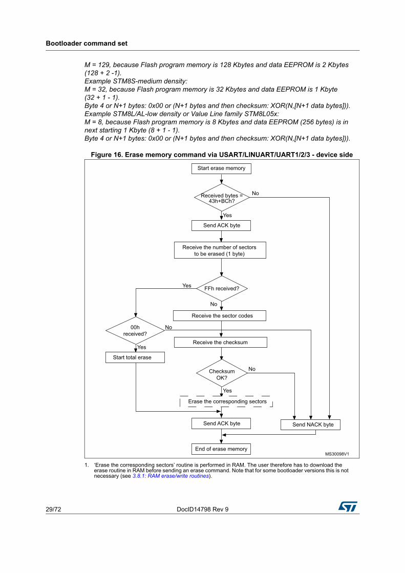
Byte 1: 0x43 - Command ID
Byte 2: 0xBC - Complement
Byte 3: 0xFF or number of sectors to be erased (0 <= N <= M); if N > M, a cmd_error occurs in the bootloader, after which the bootloader receives N + 1 data bytes and the checksum (i.e. the host completes the command).
Bootloader command set
29/72 DocID14798 Rev 9
M = 129, because Flash program memory is 128 Kbytes and data EEPROM is 2 Kbytes (128 + 2 -1).Example STM8S-medium density:M = 32, because Flash program memory is 32 Kbytes and data EEPROM is 1 Kbyte(32 + 1 - 1).Byte 4 or N+1 bytes: 0x00 or (N+1 bytes and then checksum: XOR(N,[N+1 data bytes])).Example STM8L/AL-low density or Value Line family STM8L05x:M = 8, because Flash program memory is 8 Kbytes and data EEPROM (256 bytes) is in next starting 1 Kbyte (8 + 1 - 1). Byte 4 or N+1 bytes: 0x00 or (N+1 bytes and then checksum: XOR(N,[N+1 data bytes])).
Figure 16. Erase memory command via USART/LINUART/UART1/2/3 - device side
1. ‘Erase the corresponding sectors’ routine is performed in RAM. The user therefore has to download the erase routine in RAM before sending an erase command. Note that for some bootloader versions this is not necessary (see 3.8.1: RAM erase/write routines).
DocID14798 Rev 9 30/72
Bootloader command set
71
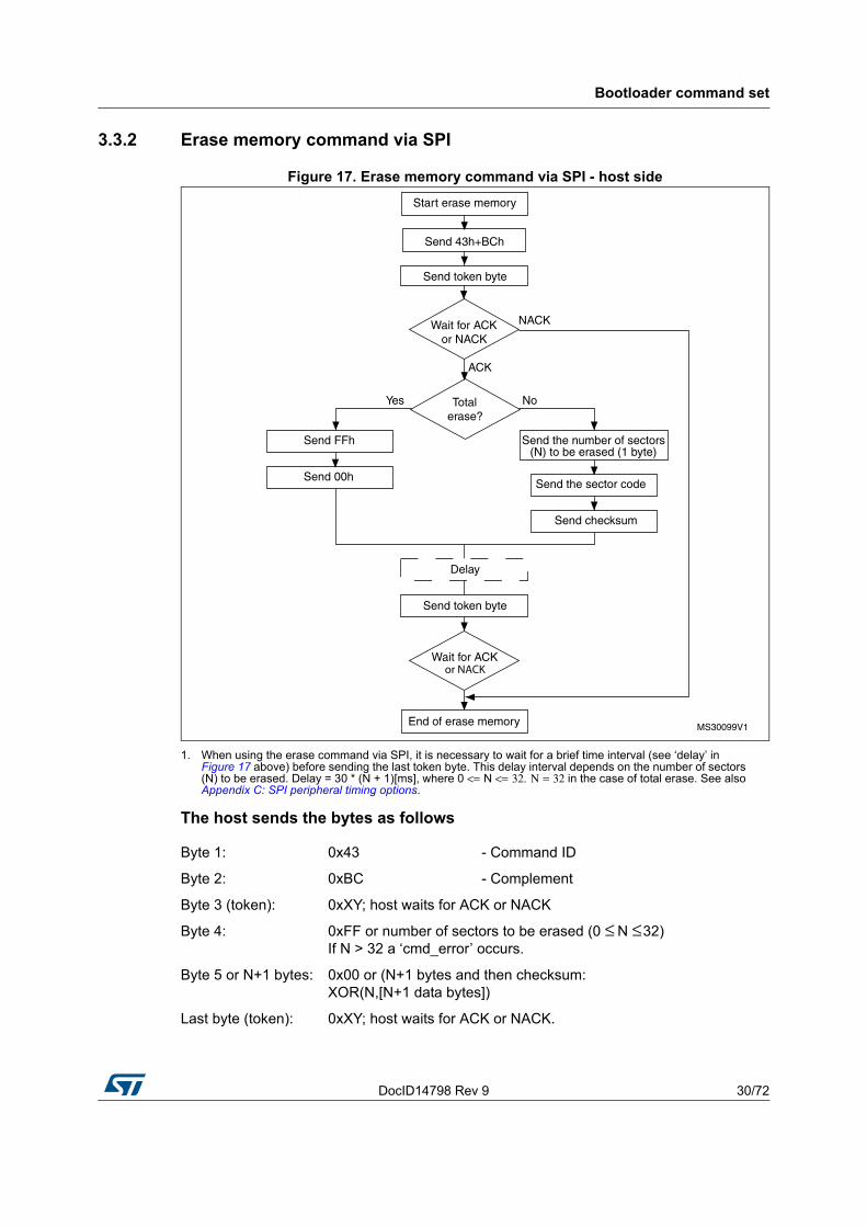
3.3.2 Erase memory command via SPI
Figure 17. Erase memory command via SPI - host side
1. When using the erase command via SPI, it is necessary to wait for a brief time interval (see ‘delay’ in Figure 17 above) before sending the last token byte. This delay interval depends on the number of sectors (N) to be erased. Delay = 30 * (N + 1)[ms], where 0 <= N <= 32. Ν = 32 in the case of total erase. See also Appendix C: SPI peripheral timing options.
The host sends the bytes as follows
Byte 1: 0x43 - Command ID
Byte 2: 0xBC - Complement
Byte 3 (token): 0xXY; host waits for ACK or NACK
Byte 4: 0xFF or number of sectors to be erased (0 ≤ N ≤ 32)If N > 32 a ‘cmd_error’ occurs.
Byte 5 or N+1 bytes: 0x00 or (N+1 bytes and then checksum: XOR(N,[N+1 data bytes])
Last byte (token): 0xXY; host waits for ACK or NACK.
Bootloader command set
31/72 DocID14798 Rev 9
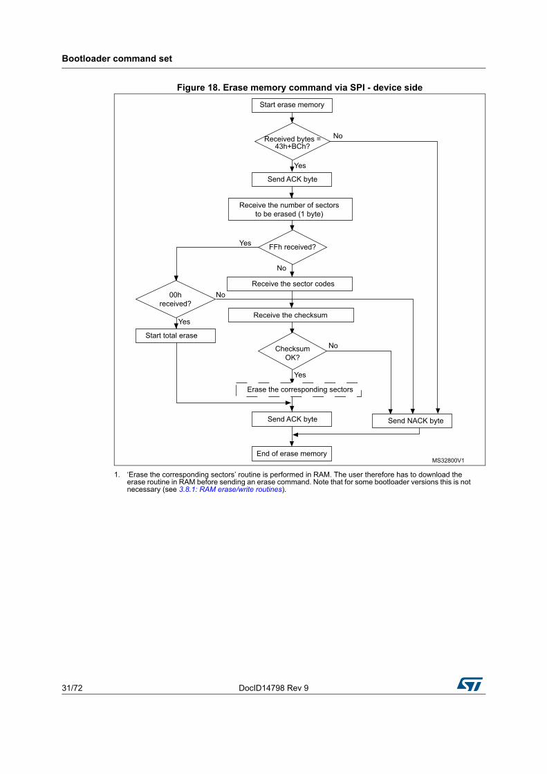
Figure 18. Erase memory command via SPI - device side
1. ‘Erase the corresponding sectors’ routine is performed in RAM. The user therefore has to download the erase routine in RAM before sending an erase command. Note that for some bootloader versions this is not necessary (see 3.8.1: RAM erase/write routines).
DocID14798 Rev 9 32/72
Bootloader command set
71
3.3.3 Erase memory command via CAN
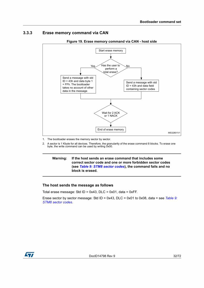
Figure 19. Erase memory command via CAN - host side
1. The bootloader erases the memory sector by sector.
2. A sector is 1 Kbyte for all devices. Therefore, the granularity of the erase command 8 blocks. To erase one byte, the write command can be used by writing 0x00.
Warning: If the host sends an erase command that includes some correct sector code and one or more forbidden sector codes (see Table 9: STM8 sector codes), the command fails and no block is erased.
The host sends the message as follows
Total erase message: Std ID = 0x43, DLC = 0x01, data = 0xFF.
Erase sector by sector message: Std ID = 0x43, DLC = 0x01 to 0x08, data = see Table 9: STM8 sector codes.
Bootloader command set
33/72 DocID14798 Rev 9
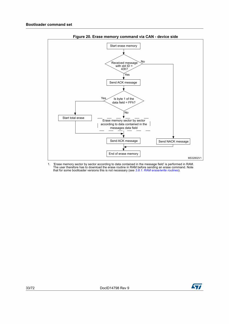
Figure 20. Erase memory command via CAN - device side
1. ‘Erase memory sector by sector according to data contained in the message field’ is performed in RAM. The user therefore has to download the erase routine in RAM before sending an erase command. Note that for some bootloader versions this is not necessary (see 3.8.1: RAM erase/write routines).
DocID14798 Rev 9 34/72
Bootloader command set
71
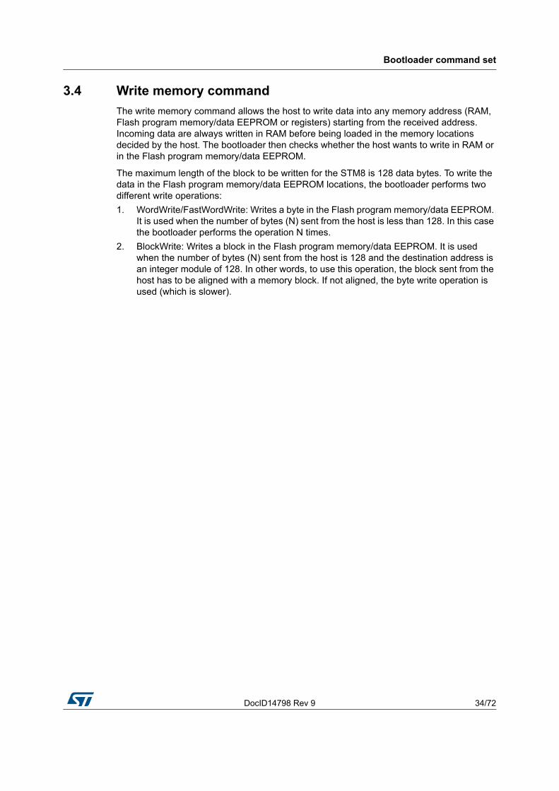
3.4 Write memory command
The write memory command allows the host to write data into any memory address (RAM, Flash program memory/data EEPROM or registers) starting from the received address. Incoming data are always written in RAM before being loaded in the memory locations decided by the host. The bootloader then checks whether the host wants to write in RAM or in the Flash program memory/data EEPROM.
The maximum length of the block to be written for the STM8 is 128 data bytes. To write the data in the Flash program memory/data EEPROM locations, the bootloader performs two different write operations:
1. WordWrite/FastWordWrite: Writes a byte in the Flash program memory/data EEPROM. It is used when the number of bytes (N) sent from the host is less than 128. In this case the bootloader performs the operation N times.
2. BlockWrite: Writes a block in the Flash program memory/data EEPROM. It is used when the number of bytes (N) sent from the host is 128 and the destination address is an integer module of 128. In other words, to use this operation, the block sent from the host has to be aligned with a memory block. If not aligned, the byte write operation is used (which is slower).
Bootloader command set
35/72 DocID14798 Rev 9
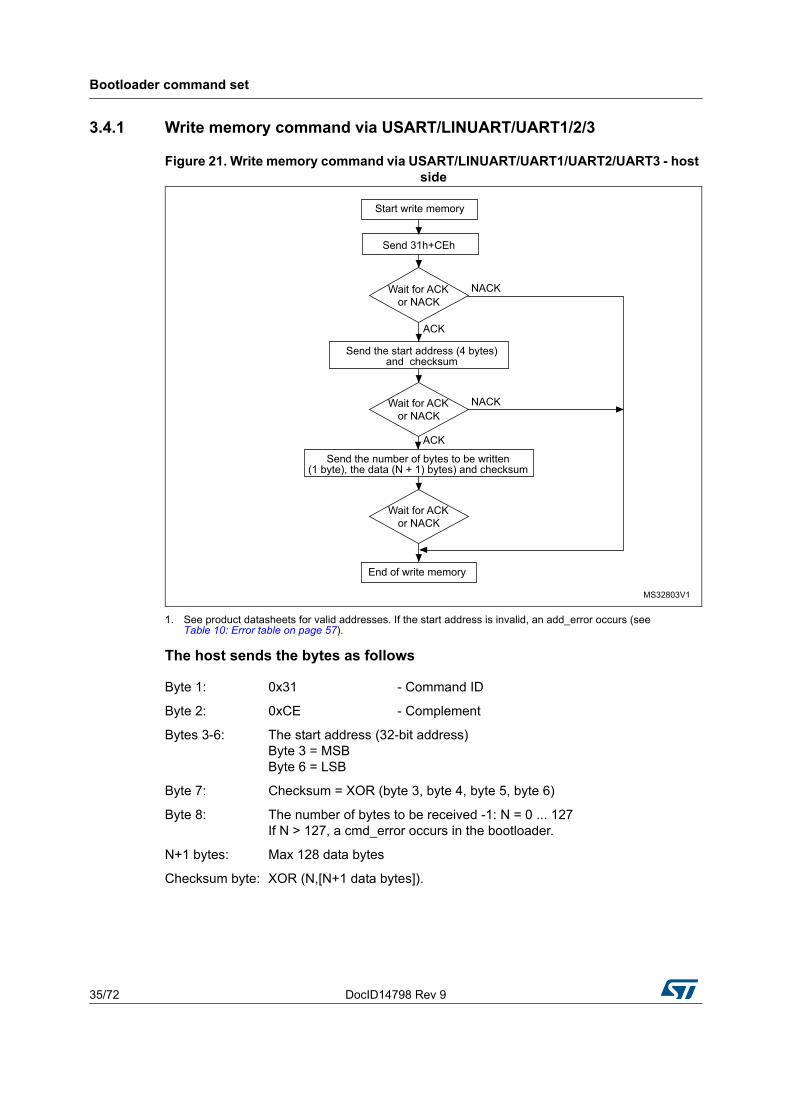
3.4.1 Write memory command via USART/LINUART/UART1/2/3
Figure 21. Write memory command via USART/LINUART/UART1/UART2/UART3 - host side
1. See product datasheets for valid addresses. If the start address is invalid, an add_error occurs (see Table 10: Error table on page 57).
Byte 8: The number of bytes to be received -1: N = 0 ... 127 If N > 127, a cmd_error occurs in the bootloader.
N+1 bytes: Max 128 data bytes
Checksum byte: XOR (N,[N+1 data bytes]).
DocID14798 Rev 9 36/72
Bootloader command set
71
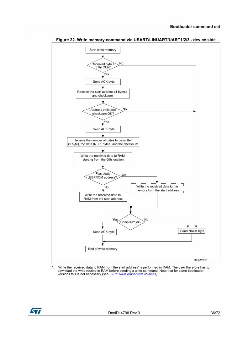
Figure 22. Write memory command via USART/LINUART/UART1/2/3 - device side
1. ‘Write the received data to RAM from the start address’ is performed in RAM. The user therefore has to download the write routine in RAM before sending a write command. Note that for some bootloader versions this is not necessary (see 3.8.1: RAM erase/write routines).
Bootloader command set
37/72 DocID14798 Rev 9
3.4.2 Write memory command via SPI
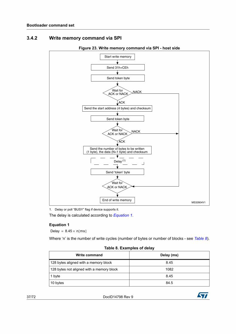
Figure 23. Write memory command via SPI - host side
1. Delay or poll “BUSY” flag if device supports it.
The delay is calculated according to Equation 1.
Equation 1
Where ‘n’ is the number of write cycles (number of bytes or number of blocks - see Table 8).
Table 8. Examples of delay
Write command Delay (ms)
128 bytes aligned with a memory block 8.45
128 bytes not aligned with a memory block 1082
1 byte 8.45
10 bytes 84.5
Delay 8.45 n ms[ ]×=
DocID14798 Rev 9 38/72
Bootloader command set
71
In SPI mode, if the device supports sending a "BUSY" flag during Flash/EEPROM memory programming, the delay can be replaced by polling the device status (a set of token bytes are sent to the device). During programming the device sends the BUSY flag (0xAA) through SPI. When the programming is finished, the device sends an ACK/NACK answer to indicate if the programming was correct or has failed.
Currently, such polling is allowed only for STM8AF/S-medium density devices with modified RAM routines (see Appendix C: SPI peripheral timing options). On STM8L/AL-low density and STM8L/AL-high/medium+ density devices, the BUSY flag is sent through the SPI interface.
The host sends the bytes as follows
Byte 1: 0x31 - Command ID
Byte 2: 0xCE - Complement
Byte 3 (token): XY; host waits for ACK or NACK
Bytes 4 to 7: The start address (32-bit address)Byte 4 = MSBByte 7 = LSB
Byte 10: The number of data bytes to be received -1: N = 0 ... 127); If N > 127, a cmd_error occurs in the bootloader.
N+1 bytes: Max 128 data bytes
Checksum byte: XOR (N,[N+1 data bytes])
Important: before sending the token byte, the host must wait for the bootloader to finish writing all data into the memory. See previous delay (or polling) description.
Last byte (token): 0xXY; host waits for ACK or NACK
Bootloader command set
39/72 DocID14798 Rev 9
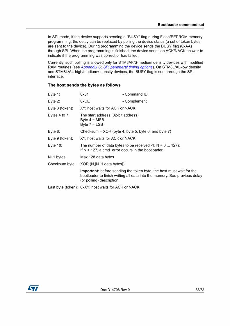
Figure 24. Write memory command via SPI - device side
1. ‘Write the received data to RAM from the start address’ is performed in RAM. The user therefore has to download the write routine in RAM before sending a write command. Note that for some bootloader versions this is not necessary (see 3.8.1: RAM erase/write routines).
DocID14798 Rev 9 40/72
Bootloader command set
71
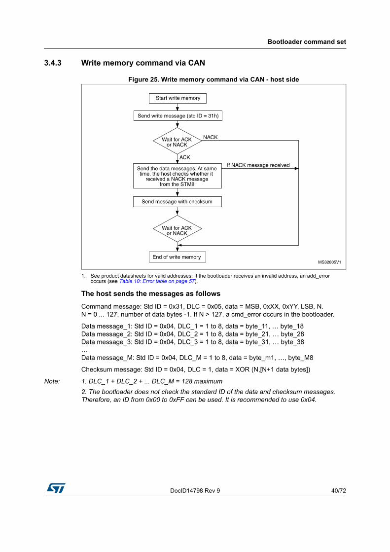
3.4.3 Write memory command via CAN
Figure 25. Write memory command via CAN - host side
1. See product datasheets for valid addresses. If the bootloader receives an invalid address, an add_error occurs (see Table 10: Error table on page 57).
The host sends the messages as follows
Command message: Std ID = 0x31, DLC = 0x05, data = MSB, 0xXX, 0xYY, LSB, N. N = 0 ... 127, number of data bytes -1. If N > 127, a cmd_error occurs in the bootloader.
Data message_1: Std ID = 0x04, DLC_1 = 1 to 8, data = byte_11, … byte_18Data message_2: Std ID = 0x04, DLC_2 = 1 to 8, data = byte_21, … byte_28Data message_3: Std ID = 0x04, DLC_3 = 1 to 8, data = byte_31, … byte_38…Data message_M: Std ID = 0x04, DLC_M = 1 to 8, data = byte_m1, …, byte_M8
Checksum message: Std ID = 0x04, DLC = 1, data = XOR (N,[N+1 data bytes])
Note: 1. DLC_1 + DLC_2 + ... DLC_M = 128 maximum
2. The bootloader does not check the standard ID of the data and checksum messages. Therefore, an ID from 0x00 to 0xFF can be used. It is recommended to use 0x04.
Bootloader command set
41/72 DocID14798 Rev 9
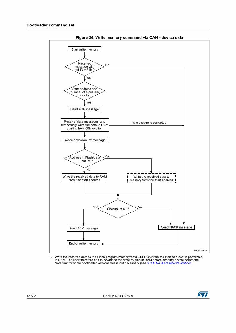
Figure 26. Write memory command via CAN - device side
1. Write the received data to the Flash program memory/data EEPROM from the start address’ is performed in RAM. The user therefore has to download the write routine in RAM before sending a write command. Note that for some bootloader versions this is not necessary (see 3.8.1: RAM erase/write routines).
DocID14798 Rev 9 42/72
Bootloader command set
71
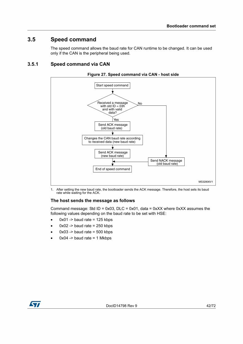
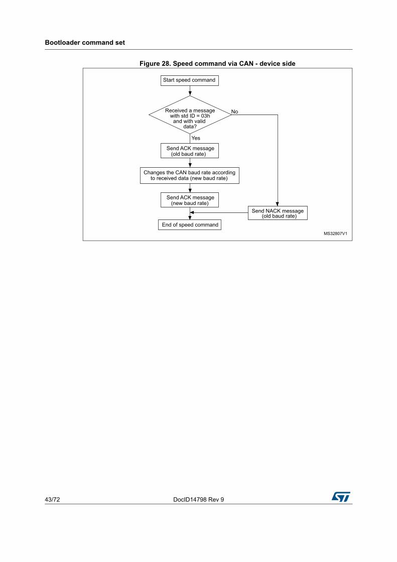
3.5 Speed command
The speed command allows the baud rate for CAN runtime to be changed. It can be used only if the CAN is the peripheral being used.
3.5.1 Speed command via CAN
Figure 27. Speed command via CAN - host side
1. After setting the new baud rate, the bootloader sends the ACK message. Therefore, the host sets its baud rate while waiting for the ACK.
The host sends the message as follows
Command message: Std ID = 0x03, DLC = 0x01, data = 0xXX where 0xXX assumes the following values depending on the baud rate to be set with HSE:
• 0x01 -> baud rate = 125 kbps
• 0x02 -> baud rate = 250 kbps
• 0x03 -> baud rate = 500 kbps
• 0x04 -> baud rate = 1 Mkbps
Bootloader command set
43/72 DocID14798 Rev 9
Figure 28. Speed command via CAN - device side
DocID14798 Rev 9 44/72
Bootloader command set
71
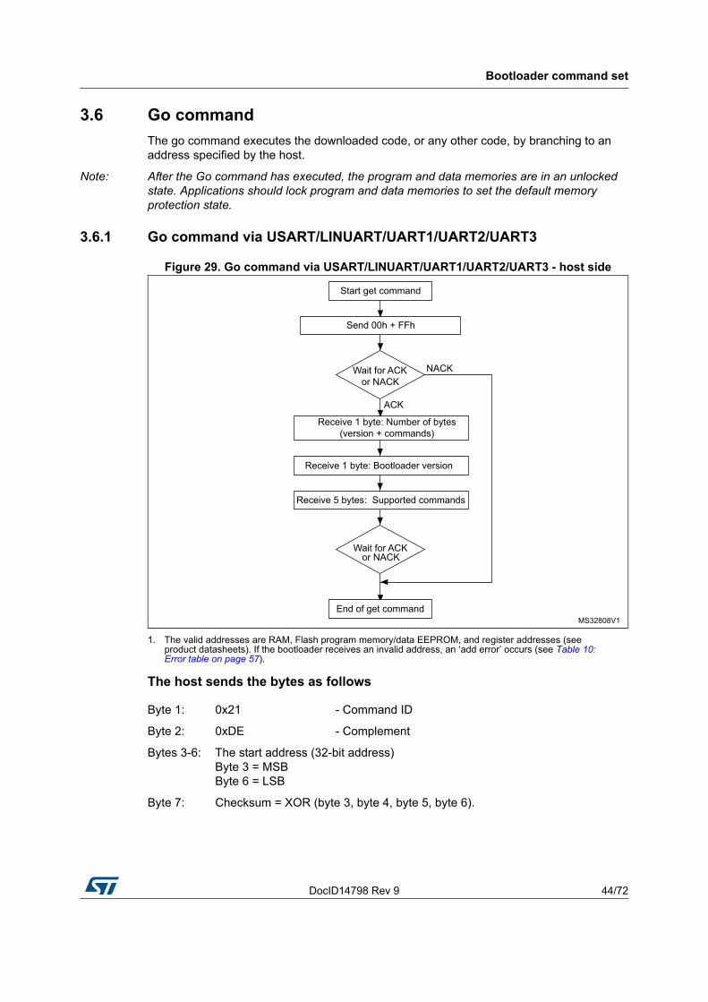
3.6 Go command
The go command executes the downloaded code, or any other code, by branching to an address specified by the host.
Note: After the Go command has executed, the program and data memories are in an unlocked state. Applications should lock program and data memories to set the default memory protection state.
3.6.1 Go command via USART/LINUART/UART1/UART2/UART3
Figure 29. Go command via USART/LINUART/UART1/UART2/UART3 - host side
1. The valid addresses are RAM, Flash program memory/data EEPROM, and register addresses (see product datasheets). If the bootloader receives an invalid address, an ‘add error’ occurs (see Table 10: Error table on page 57).
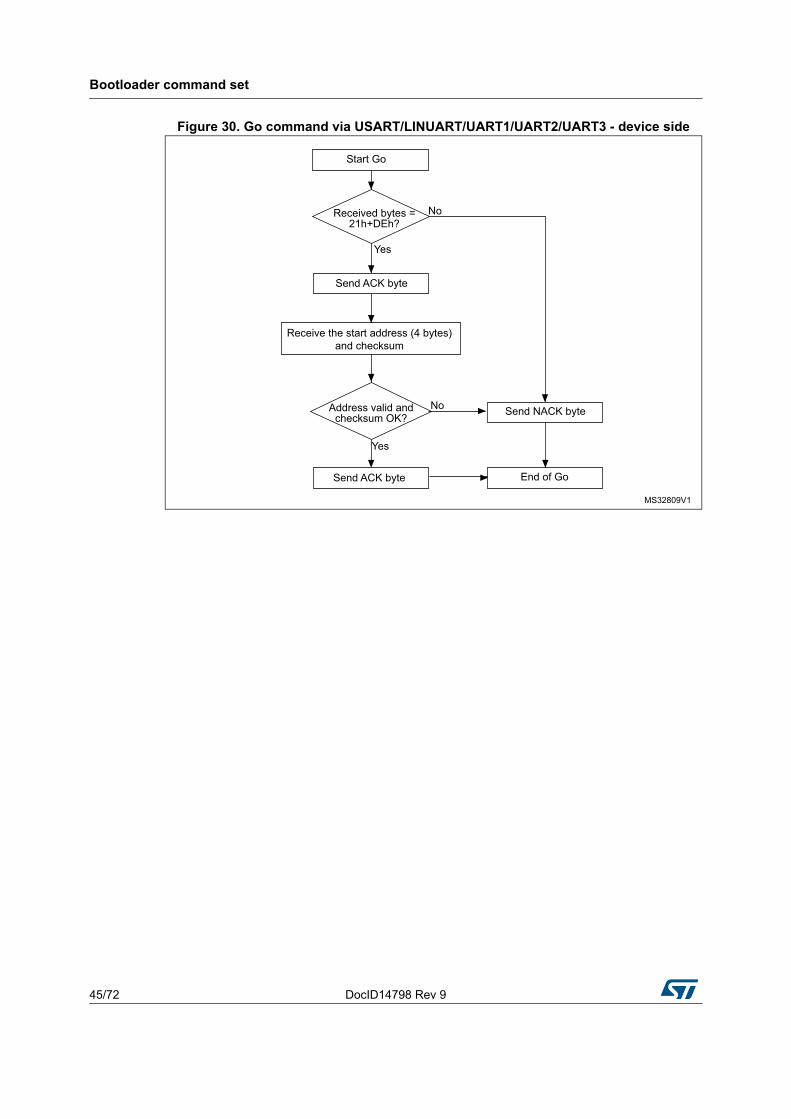
Figure 30. Go command via USART/LINUART/UART1/UART2/UART3 - device side
DocID14798 Rev 9 46/72
Bootloader command set
71
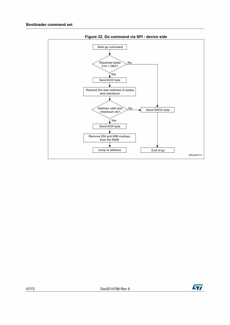
3.6.2 Go command via SPI
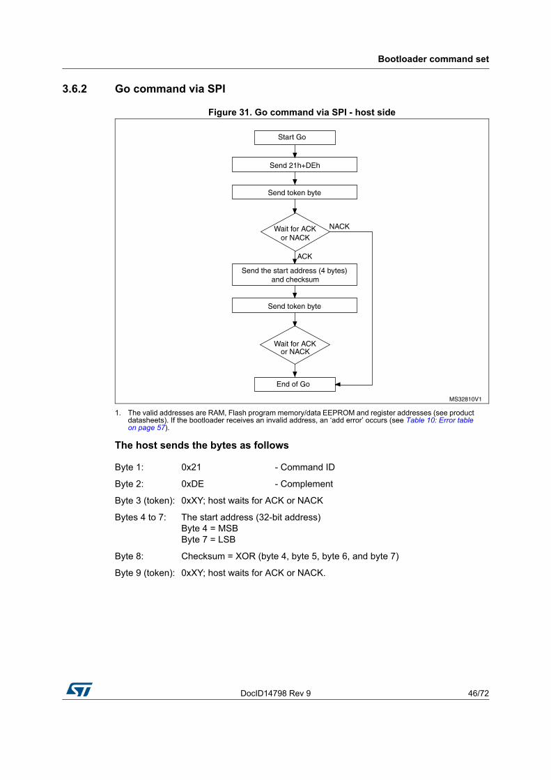
Figure 31. Go command via SPI - host side
1. The valid addresses are RAM, Flash program memory/data EEPROM and register addresses (see product datasheets). If the bootloader receives an invalid address, an ‘add error’ occurs (see Table 10: Error table on page 57).
The host sends the bytes as follows
Byte 1: 0x21 - Command ID
Byte 2: 0xDE - Complement
Byte 3 (token): 0xXY; host waits for ACK or NACK
Bytes 4 to 7: The start address (32-bit address)Byte 4 = MSBByte 7 = LSB
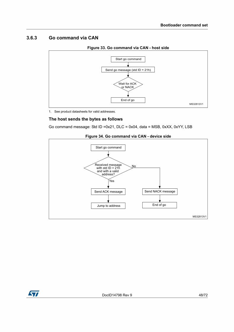
Go command message: Std ID =0x21, DLC = 0x04, data = MSB, 0xXX, 0xYY, LSB
Figure 34. Go command via CAN - device side
Bootloader command set
49/72 DocID14798 Rev 9
3.7 Sector codes
Table 9. STM8 sector codes
Sector code
Flash program memory/data EEPROM
STM8AF/S-high density
STM8AF/S-medium density
STM8L/AL-medium density
STM8L/AL-high/medium+
density
STM8L-low density or Value Line family
STM8L05x
0x000x00 8000 -> 0x00 83FF
0x00 8000 -> 0x00 83FF
0x00 8000 -> 0x00 83FF
0x00 8000 -> 0x00 83FF
0x00 8000 -> 0x00 83FF
0x010x00 8400 -> 0x00 87FF
0x00 8400 -> 0x00 87FF
0x00 8400 -> 0x00 87FF
0x00 8400 -> 0x00 87FF
0x00 8400 -> 0x00 87FF
0x020x00 8800 -> 0x00 8BFF
0x00 8800 -> 0x00 8BFF
0x00 8800 -> 0x00 8BFF
0x00 8800 -> 0x00 8BFF
0x00 8800 -> 0x00 8BFF
0x030x00 8C00 ->
0x00 8FFF0x00 8C00 ->
0x00 8FFF0x00 8C00 ->
0x00 8FFF0x00 8C00 ->
0x00 8FFF0x00 8C00 ->
0x00 8FFF
0x040x00 9000 -> 0x00 93FF
0x00 9000 -> 0x00 93FF
0x00 9000 -> 0x00 93FF
0x00 9000 -> 0x00 93FF
0x00 9000 -> 0x00 93FF
0x050x00 9400 -> 0x00 97FF
0x00 9400 -> 0x00 97FF
0x00 9400 -> 0x00 97FF
0x00 9400 -> 0x00 97FF
0x00 9400 -> 0x00 97FF
0x060x00 9800 -> 0x00 9BFF
0x00 9800 -> 0x00 9BFF
0x00 9800 -> 0x00 9BFF
0x00 9800 -> 0x00 9BFF
0x00 9800 -> 0x00 9BFF
0x070x00 9C00 ->
0x00 9FFF0x00 9C00 ->
0x00 9FFF0x00 9C00 ->
0x00 9FFF0x00 9C00 ->
0x00 9FFF0x00 9C00 ->
0x00 9FFF
0x080x00 A000 -> 0x00 A3FF
0x00 A000 -> 0x00 A3FF
0x00 A000 -> 0x00 A3FF
0x00 A000 -> 0x00 A3FF
0x00 1000 -> 0x00 10FF
0x090x00 A400 -> 0x00 A7FF
0x00 A400 -> 0x00 A7FF
0x00 A400 -> 0x00 A7FF
0x00 A400 -> 0x00 A7FF
-
0x0A0x00 A800 -> 0x00 ABFF
0x00 A800 -> 0x00 ABFF
0x00 A800 -> 0x00 ABFF
0x00 A800 -> 0x00 ABFF
-
0x0B0x00 AC00 ->
0x00 AFFF0x00 AC00 ->
0x00 AFFF0x00 AC00 ->
0x00 AFFF0x00 AC00 ->
0x00 AFFF-
0x0C0x00 B000 -> 0x00 B3FF
0x00 B000 -> 0x00 B3FF
0x00 B000 -> 0x00 B3FF
0x00 B000 -> 0x00 B3FF
-
0D0x00 B400 -> 0x00 B7FF
0x00 B400 -> 0x00 B7FF
0x00 B400 -> 0x00 B7FF
0x00 B400 -> 0x00 B7FF
-
0x0E0x00 B800 -> 0x00 BBFF
0x00 B800 -> 0x00 BBFF
0x00 B800 -> 0x00 BBFF
0x00 B800 -> 0x00 BBFF
-
0x0F0x00 BC00 ->
0x00 BFFF0x00 BC00 ->
0x00 BFFF0x00 BC00 ->
0x00 BFFF0x00 BC00 ->
0x00 BFFF-
0x100x00 C000 -> 0x00 C3FF
0x00 C000 -> 0x00 C3FF
0x00 C000 -> 0x00 C3FF
0x00 C000 -> 0x00 C3FF
-
0x110x00 C400 -> 0x00 C7FF
0x00 C400 -> 0x00 C7FF
0x00 C400 -> 0x00 C7FF
0x00 C400 -> 0x00 C7FF
-
DocID14798 Rev 9 50/72
Bootloader command set
71
0x120x00 C800 -> 0x00 CBFF
0x00 C800 -> 0x00 CBFF
0x00 C800 -> 0x00 CBFF
0x00 C800 -> 0x00 CBFF
-
0x130x00 CC00 ->
0x00 CFFF0x00 CC00 ->
0x00 CFFF0x00 CC00 ->
0x00 CFFF0x00 CC00 ->
0x00 CFFF-
0x140x00 D000 -> 0x00 D3FF
0x00 D000 -> 0x00 D3FF
0x00 D000 -> 0x00 D3FF
0x00 D000 -> 0x00 D3FF
-
0x150x00 D400 -> 0x00 D7FF
0x00 D400 -> 0x00 D7FF
0x00 D400 -> 0x00 D7FF
0x00 D400 -> 0x00 D7FF
-
0x160x00 D800 -> 0x00 DBFF
0x00 D800 -> 0x00 DBFF
0x00 D800 -> 0x00 DBFF
0x00 D800 -> 0x00 DBFF
-
0x170x00 DC00 ->
0x00 DFFF0x00 DC00 ->
0x00 DFFF0x00 DC00 ->
0x00 DFFF0x00 DC00 ->
0x00 DFFF-
0x180x00 E000 -> 0x00 E3FF
0x00 E000 -> 0x00 E3FF
0x00 E000 -> 0x00 E3FF
0x00 E000 -> 0x00 E3FF
-
0x190x00 E400 -> 0x00 E7FF
0x00 E400 -> 0x00 E7FF
0x00 E400 -> 0x00 E7FF
0x00 E400 -> 0x00 E7FF
-
0x1A0x00 E800 -> 0x00 EBFF
0x00 E800 -> 0x00 EBFF
0x00 E800 -> 0x00 EBFF
0x00 E800 -> 0x00 EBFF
-
0x1B0x00 EC00 ->
0x00 EFFF0x00 EC00 ->
0x00 EFFF0x00 EC00 ->
0x00 EFFF0x00 EC00 ->
0x00 EFFF-
0x1C0x00 F000 -> 0x00 F3FF
0x00 F000 -> 0x00 F3FF
0x00 F000 -> 0x00 F3FF
0x00 F000 -> 0x00 F3FF
-
0x1D0x00 F400 -> 0x00 F7FF
0x00 F400 -> 0x00 F7FF
0x00 F400 -> 0x00 F7FF
0x00 F400 -> 0x00 F7FF
-
0x1E0x00 F800 -> 0x00 FBFF
0x00 F800 -> 0x00 FBFF
0x00 F800 -> 0x00 FBFF
0x00 F800 -> 0x00 FBFF
-
0x1F0x00 FC00 ->
0x00 FFFF0x00 FC00 ->
0x00 FFFF0x00 FC00 ->
0x00 FFFF0x00 FC00 ->
0x00 FFFF-
0x200x01 0000 -> 0x01 03FF
0x00 4000 -> 0x00 43FF
0x00 1000 -> 0x00 13FF
0x01 0000 -> 0x01 03FF
-
0x210x01 0400 ->
0x1 07FF- -
0x01 0400 -> 0x1 07FF
-
0x220x01 0800 -> 0x01 0BFF
- -0x01 0800 -> 0x01 0BFF
-
0x230x01 0C00 ->
0x01 0FFF- -
0x01 0C00 -> 0x01 0FFF
-
0x240x01 1000 -> 0x01 13FF
- -0x01 1000 -> 0x01 13FF
-
Table 9. STM8 sector codes (continued)
Sector code
Flash program memory/data EEPROM
STM8AF/S-high density
STM8AF/S-medium density
STM8L/AL-medium density
STM8L/AL-high/medium+
density
STM8L-low density or Value Line family
STM8L05x
Bootloader command set
51/72 DocID14798 Rev 9
0x250x01 1400 -> 0x01 17FF
- -0x01 1400 -> 0x01 17FF
-
0x260x01 1800 -> 0x01 1BFF
- -0x01 1800 -> 0x01 1BFF
-
0x270x01 1C00 ->
0x01 1FFF- -
0x01 1C00 -> 0x01 1FFF
-
0x280x01 2000 -> 0x01 23FF
- -0x01 2000 -> 0x01 23FF
-
0x290x01 2400 -> 0x01 27FF
- -0x01 2400 -> 0x01 27FF
-
0x2A0x01 2800 -> 0x01 2BFF
- -0x01 2800 -> 0x01 2BFF
-
0x2B0x01 2C00 ->
0x01 2FFF- -
0x01 2C00 -> 0x01 2FFF
-
0x2C0x01 3000 -> 0x01 33FF
- -0x01 3000 -> 0x01 33FF
-
0x2D0x01 3400 -> 0x01 37FF
- -0x01 3400 -> 0x01 37FF
-
0x2E0x01 3800 -> 0x01 3BFF
- -0x01 3800 -> 0x01 3BFF
-
0x2F0x01 3C00 ->
0x01 3FFF- -
0x01 3C00 -> 0x01 3FFF
-
0x300x01 4000 -> 0x01 43FF
- -0x01 4000 -> 0x01 43FF
-
0x310x01 4400 -> 0x01 47FF
- -0x01 4400 -> 0x01 47FF
-
0x320x01 4800 -> 0x01 4BFF
- -0x01 4800 -> 0x01 4BFF
-
0x330x01 4C00 ->
0x01 4FFF- -
0x01 4C00 -> 0x01 4FFF
-
0x340x01 1000 -> 0x01 53FF
- -0x01 1000 -> 0x01 53FF
-
0x350x01 5400 -> 0x01 57FF
- -0x01 5400 -> 0x01 57FF
-
0x360x01 5800 -> 0x01 5BFF
- -0x01 5800 -> 0x01 5BFF
-
0x370x01 5C00 ->
0x01 5FFF- -
0x01 5C00 -> 0x01 5FFF
-
Table 9. STM8 sector codes (continued)
Sector code
Flash program memory/data EEPROM
STM8AF/S-high density
STM8AF/S-medium density
STM8L/AL-medium density
STM8L/AL-high/medium+
density
STM8L-low density or Value Line family
STM8L05x
DocID14798 Rev 9 52/72
Bootloader command set
71
0x380x01 6000 -> 0x01 63FF
- -0x01 6000 -> 0x01 63FF
-
0x390x01 6400 -> 0x01 67FF
- -0x01 6400 -> 0x01 67FF
-
0x3A0x01 6800 -> 0x01 6BFF
- -0x01 6800 -> 0x01 6BFF
-
0x3B0x01 6C00 ->
0x01 6FFF- -
0x01 6C00 -> 0x01 6FFF
-
0x3C0x01 7000 -> 0x01 73FF
- -0x01 7000 -> 0x01 73FF
-
0x3D0x01 7400 -> 0x01 77FF
- -0x01 7400 -> 0x01 77FF
-
0x3E0x01 7800 -> 0x01 7BFF
- -0x01 7800 -> 0x01 7BFF
-
0x3F0x01 7C00 ->
0x01 7FFF- -
0x01 7C00 -> 0x01 7FFF
-
0x400x01 8000 -> 0x01 83FF
- -0x00 1000 -> 0x00 13FF
-
0x410x01 8400 -> 0x01 87FF
- -0x00 1400 -> 0x00 17FF
-
0x420x01 8800 -> 0x01 8BFF
- - - -
0x430x01 8C00 -> 0x01 18FFF
- - - -
0x440x01 9000 -> 0x01 93FF
- - - -
0x450x01 9400 -> 0x01 97FF
- - - -
0x460x01 9800 -> 0x01 9BFF
- - - -
0x470x01 9C00 ->
0x01 9FFF- - - -
0x480x01 A000 -> 0x01 A3FF
- - - -
0x490x01 A400 -> 0x01 A7FF
- - - -
0x4A0x01 A800 -> 0x01 ABFF
- - - -
Table 9. STM8 sector codes (continued)
Sector code
Flash program memory/data EEPROM
STM8AF/S-high density
STM8AF/S-medium density
STM8L/AL-medium density
STM8L/AL-high/medium+
density
STM8L-low density or Value Line family
STM8L05x
Bootloader command set
53/72 DocID14798 Rev 9
0x4B0x01 AC00 ->
0x01 AFFF- - - -
0x4C0x01 B000 -> 0x01 B3FF
- - - -
0x4D0x01 B400 -> 0x01 B7FF
- - - -
0x4E0x01 B800 -> 0x01 BBFF
- - - -
0x4F0x01 BC00 ->
0x01 BFFF- - - -
0x500x01 C000 -> 0x01 C3FF
- - - -
0x510x01 C400 -> 0x01 C7FF
- - - -
0x520x01 C800 -> 0x01 CBFF
- - - -
0x530x01 CC00 ->
0x01 CFFF- - - -
0x540x01 D000 -> 0x01 D3FF
- - - -
0x550x01 D400 -> 0x01 D7FF
- - - -
0x560x01 D800 -> 0x01 DBFF
- - - -
0x570x01 DC00 ->
0x01 DFFF- - - -
0x580x01 E000 -> 0x01 E3FF
- - - -
0x590x01 E400 -> 0x01 E7FF
- - - -
0x5A0x01 E800 -> 0x01 EBFF
- - - -
0x5B0x01 EC00 ->
0x01 EFFF- - - -
0x5C0x01 F000 -> 0x01 F3FF
- - - -
0x5D0x01 F400 -> 0x01 F7FF
- - - -
Table 9. STM8 sector codes (continued)
Sector code
Flash program memory/data EEPROM
STM8AF/S-high density
STM8AF/S-medium density
STM8L/AL-medium density
STM8L/AL-high/medium+
density
STM8L-low density or Value Line family
STM8L05x
DocID14798 Rev 9 54/72
Bootloader command set
71
0x5E0x10 F800 -> 0x10 FBFF
- - - -
0x5F0x10 FC00 ->
0x10 FFFF- - - -
0x600x20 0000 -> 0x20 03FF
- - - -
0x610x20 0400 -> 0x20 07FF
- - - -
0x620x02 0800 -> 0x02 0BFF
- - - -
0x630x02 0C00 ->
0x02 0FFF- - - -
0x640x02 1000 -> 0x02 13FF
- - - -
0x650x02 1400 -> 0x02 17FF
- - - -
0x660x02 1800 -> 0x02 1BFF
- - - -
0x670x02 1C00 ->
0x02 1FFF- - - -
0x680x02 2000 -> 0x02 23FF
- - - -
0x690x02 2400 -> 0x02 27FF
- - - -
0x6A0x02 2800 -> 0x02 2BFF
- - - -
0x6B0x02 2C00 ->
0x02 2FFF- - - -
0x6C0x02 2000 -> 0x02 23FF
- - - -
0x6D0x02 2400 ->0x02 27FF
- - - -
0x6E0x02 3800 -> 0x02 3BFF
- - - -
0x6F0x02 3C00 ->
0x02 3FFF- - - -
0x700x02 4000 -> 0x02 43FF
- - - -
Table 9. STM8 sector codes (continued)
Sector code
Flash program memory/data EEPROM
STM8AF/S-high density
STM8AF/S-medium density
STM8L/AL-medium density
STM8L/AL-high/medium+
density
STM8L-low density or Value Line family
STM8L05x
Bootloader command set
55/72 DocID14798 Rev 9
0x710x02 4400 -> 0x02 47FF
- - - -
0x720x02 4800 -> 0x02 4BFF
- - - -
0x730x02 4C00 ->
0x02 4FFF- - - -
0x740x02 5000 -> 0x02 53FF
- - - -
0x750x02 5400 -> 0x02 57FF
- - - -
0x760x02 5800 -> 0x02 5BFF
- - - -
0x770x02 5C00 ->
0x02 5FFF- - - -
0x780x02 6000 -> 0x02 63FF
- - - -
0x790x02 6400 -> 0x02 67FF
- - - -
0x7A0x0 26800 -> 0x0 26BFF
- - - -
0x7B0x02 6C00 ->
0x0 26FFF- - - -
0x7C0x02 7000 -> 0x02 73FF
- - - -
0x7D0x02 7400 -> 0x02 77FF
- - - -
0x7E0x02 7800 -> 0x02 7BFF
- - - -
0x7F0x02 7C00 ->
0x02 7FFF- - - -
0x800x00 4000 -> 0x00 43FF
- - - -
0x810x00 4400 -> 0x00 47FF
- - - -
Table 9. STM8 sector codes (continued)
Sector code
Flash program memory/data EEPROM
STM8AF/S-high density
STM8AF/S-medium density
STM8L/AL-medium density
STM8L/AL-high/medium+
density
STM8L-low density or Value Line family
STM8L05x
DocID14798 Rev 9 56/72
Bootloader command set
71
3.8 Software model (STM8AF/AL/L/S)
The boot code has been designed with the same logical protocol for exchanging command frames between host and any STM8AF/AL/L/S device.
The boot code can download up to 128 bytes at a time. Bootloader variables occupy the RAM from address 0x00 0000 up to address 0x00 009F.
If the bootloader is enabled (according to Table 4) and timeouts have elapsed (there is no host activation or jump to the user application), the RAM content can be modified by the bootloader. For example, if the user application is running and a reset occurs, the RAM content in a given range is changed by the bootloader before the application restarts.
If the bootloader is disabled by using an option byte or ROP protection, the following minor modifications of the user application are needed:
• STM8L/AL devices and latest STM8AF/S bootloader versions (see Table 3): the RAM is not modified.
• STM8AF/S devices with older bootloader versions: RAM is modified at addresses 0x00 0095 and 0x00 0099.
Note: Unused (empty) bootloader ROM is filled with an opcode that is not allowed (0x71). If, for any reason (i.e. EMC noise), the core starts to execute in the 0x71 area, an illegal opcode is returned and consequently a reset. This prevents the bootloader falling into an infinite loop with no reset in the event that it jumps in the ‘empty’ locations. Thus normal execution can resume.
3.8.1 RAM erase/write routines
RAM erase/write routines are attached to this document as binary code files in S19 format. The file name defines the STM8 group (e.g.128 Kbytes, 32 Kbytes, 8 Kbytes) and bootloader version number for which the given routine is written.
To erase or program the Flash program memory or data EEPROM, the respective routines must be downloaded into RAM starting at 0x00 00A0.
• STM8L/AL 8-Kbyte (low density) devices: E_W_ROUTINEs_8K_verL_1.0.s19 (this is just patch for internally stored RAM routine: load of one byte 0xB2 to address 0x01EA)
• STM8L/AL devices: no need to download RAM routines - the routines are copied into RAM from ROM automatically when the bootloader is activated by the host (after it has received a valid SYNCH byte)
Note: To execute any of the commands (get, read, erase, write, speed, and go), the bootloader uses part of the RAM for its own variables and RAM erase/write routines. Therefore, it is forbidden to run write commands (with the exception of write commands that are used for downloading erase/write routines) with destination addresses in the following RAM locations:
• STM8AF/S devices: 0x00 0000 to 0x00 01FF
• STM8L/AL devices: 0x00 0000 to 0x00 01FF
Error management
57/72 DocID14798 Rev 9
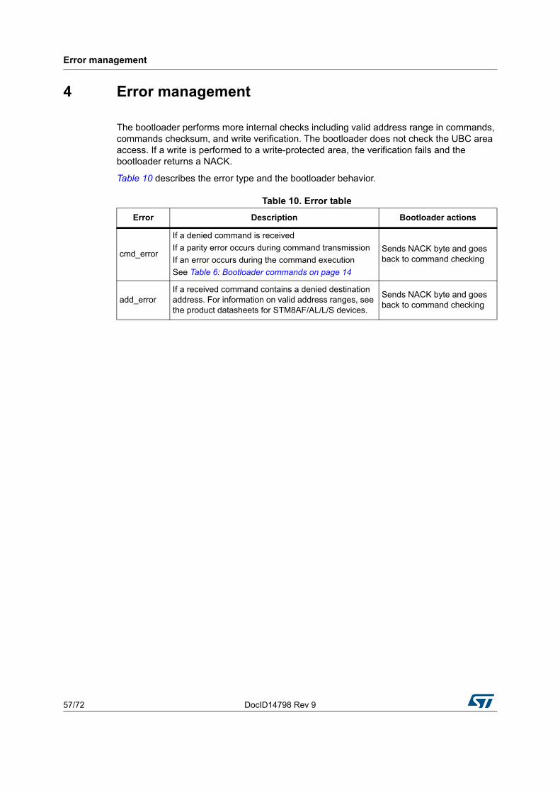
4 Error management
The bootloader performs more internal checks including valid address range in commands, commands checksum, and write verification. The bootloader does not check the UBC area access. If a write is performed to a write-protected area, the verification fails and the bootloader returns a NACK.
Table 10 describes the error type and the bootloader behavior.
Table 10. Error table
Error Description Bootloader actions
cmd_error
If a denied command is received
If a parity error occurs during command transmission
If an error occurs during the command execution
See Table 6: Bootloader commands on page 14
Sends NACK byte and goes back to command checking
add_errorIf a received command contains a denied destination address. For information on valid address ranges, see the product datasheets for STM8AF/AL/L/S devices.
Sends NACK byte and goes back to command checking
DocID14798 Rev 9 58/72
Programming time
71
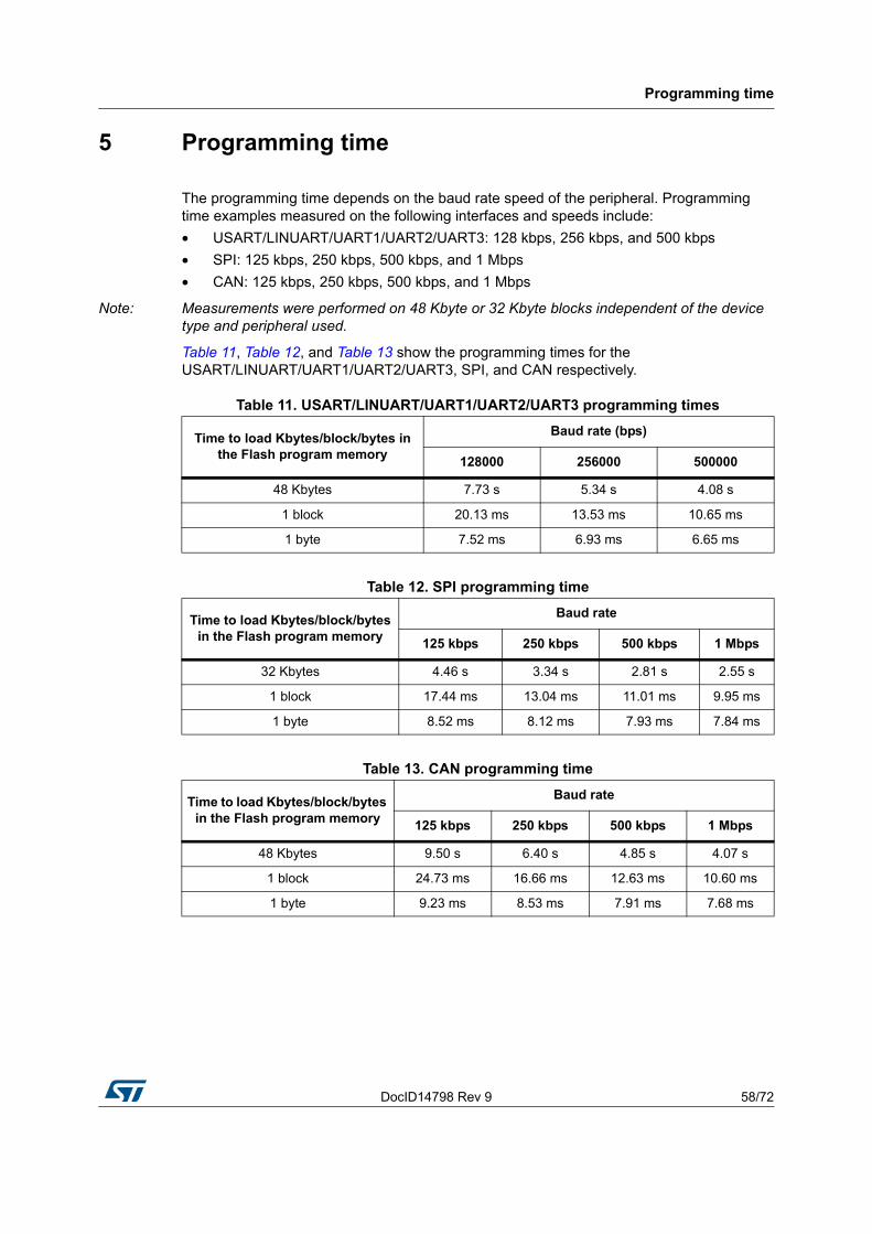
5 Programming time
The programming time depends on the baud rate speed of the peripheral. Programming time examples measured on the following interfaces and speeds include:
• USART/LINUART/UART1/UART2/UART3: 128 kbps, 256 kbps, and 500 kbps
• SPI: 125 kbps, 250 kbps, 500 kbps, and 1 Mbps
• CAN: 125 kbps, 250 kbps, 500 kbps, and 1 Mbps
Note: Measurements were performed on 48 Kbyte or 32 Kbyte blocks independent of the device type and peripheral used.
Table 11, Table 12, and Table 13 show the programming times for the USART/LINUART/UART1/UART2/UART3, SPI, and CAN respectively.
Table 11. USART/LINUART/UART1/UART2/UART3 programming times
Time to load Kbytes/block/bytes in the Flash program memory
Baud rate (bps)
128000 256000 500000
48 Kbytes 7.73 s 5.34 s 4.08 s
1 block 20.13 ms 13.53 ms 10.65 ms
1 byte 7.52 ms 6.93 ms 6.65 ms
Table 12. SPI programming time
Time to load Kbytes/block/bytes in the Flash program memory
Baud rate
125 kbps 250 kbps 500 kbps 1 Mbps
32 Kbytes 4.46 s 3.34 s 2.81 s 2.55 s
1 block 17.44 ms 13.04 ms 11.01 ms 9.95 ms
1 byte 8.52 ms 8.12 ms 7.93 ms 7.84 ms
Table 13. CAN programming time
Time to load Kbytes/block/bytes in the Flash program memory
Baud rate
125 kbps 250 kbps 500 kbps 1 Mbps
48 Kbytes 9.50 s 6.40 s 4.85 s 4.07 s
1 block 24.73 ms 16.66 ms 12.63 ms 10.60 ms
1 byte 9.23 ms 8.53 ms 7.91 ms 7.68 ms
How to upgrade ROP protected device
59/72 DocID14798 Rev 9
Appendix A How to upgrade ROP protected device
The readout protection (ROP) feature prevents the device memory content being read through the SWIM interface. During its initialization, the bootloader checks the ROP state (by checking the ROP option byte) and if it is enabled the bootloader is not activated. This prevents the memory content being read through the bootloader (or a Trojan horse being written and executed).
However, in practice, the user may need to have the ROP protection enabled and still be able to upload new firmware through IAP (in-application programming). This can be done via a user application and bootloader interaction, subject to the following rules.
A.1 Rules for upgrading ROP protected devices
1. The device must be ROP protected (to disable reading through the SWIM).
2. The bootloader is not activated after reset due to the check on the ROP state (to disable reading through the bootloader).
3. The user application is responsible for enabling a device update after user authentication, for example, after a user password check.
4. The user application then allows the authenticated user to invoke the bootloader (by jumping to a bootloader specific address). The bootloader can then update the user application in the normal way.
Following the above rules, the user application can be updated by the resident ROM bootloader. The only condition is that the user application must interact with the upload process as outlined below:
• The application must implement an authentication procedure (for example by sending an authentication command with a password through the communication interface).
• The application must jump to the “ROP check” in which the bootloader entry point is checked. See Table 14: Bootloader entry points for the addresses of the principle bootloader entry points.
DocID14798 Rev 9 60/72
Bootloader entry points
71
Appendix B Bootloader entry points
The ROM bootloader can be activated by the host after device reset. However the bootloader can also be used by the user application for various purposes. Table 14 lists the main bootloader entry points and describes how they can be used by the user application.
Table 14. Bootloader entry points
Before jumping to the entry point, the user application must configure all used peripherals (timers, communication peripherals, GPIO pins on communication peripherals) to their reset state to be able to continue correctly in bootloader. Bootloader is designed to be run after device reset where all peripherals are in reset state.
Entry point name
Address and bootloader version(1)
UsageSTM8AF/S-
high density
STM8AF/S-medium density
STM8L/AL-medium density
STM8L/AL-high/medium
+ density
STM8L/AL-low density
Reset 0x00 6000 0x00 6000 0x00 6000 0x00 6000 0x00 6000Bootloader starts here. Can be used to perform a hard reset
BL option check
0x00 601E (v2.1)(2)
0x00 601E (v2.2)
0x00 601E (v1.2)(3)
0x00 6018 (v1.3)
0x00 601A (v1.1)
0x00 601F (v1.2)
0x00 601F (v1.1)
0x00 601F (v1.0)
Point after checking if bootloader is enabled by option byte. Can be used to jump to the bootloader which was disabled by the option bytes.
ROP check
0x00 602E (v2.1)(2)
0x00 602E (v2.2)
0x00 602E (v1.2)(3)
0x00 6028 (v1.3)
0x00 6028 (v1.1)
0x00 602D (v1.2)(4)
0x00 602D (v1.1)
0x00 602D (v1.0)
Point after checking readout protection. Can be used to jump to the bootloader - if ROP is active - for upgrading an ROP-protected device after master user authentication.
1. The address depends on the bootloader version and may be changed in the next bootloader version. Contact your local STMicroelectronics office for the latest information.
2. The RAM variable at address 0x00 0099 should be set to the value 0x00 or 0x01 for this bootloader version (0x00 = no timeout, 0x01 = 1 second bootloader timeout).
3. The RAM variable at address 0x00 0095 should be set to the value 0x00 or 0x01 for this bootloader version (0x00 = no timeout, 0x01 = 1 second bootloader timeout).
4. No ROP check entry point is defined for bootloader version 1.0.
Bootloader entry points
61/72 DocID14798 Rev 9
Note: For all devices, before jumping to the bootloader entry point, it is necessary to refresh the TIM2 and TIM3 prescaler shadow registers to value 1 with the following recommended code:
...
TIM3->EGR = 0x01; // invoke update event to refresh TIM3 prescaler to 1
TIM3->SR1; // clear generated update event flag in TIM3_SR1 by reading it
TIM3->SR1 = 0x00; // and by writing zero to it
_asm("jp 0x601E"); // jump to given entry point address
...
DocID14798 Rev 9 62/72
SPI peripheral timing options
71
Appendix C SPI peripheral timing options
C.1 SPI with busy state checking
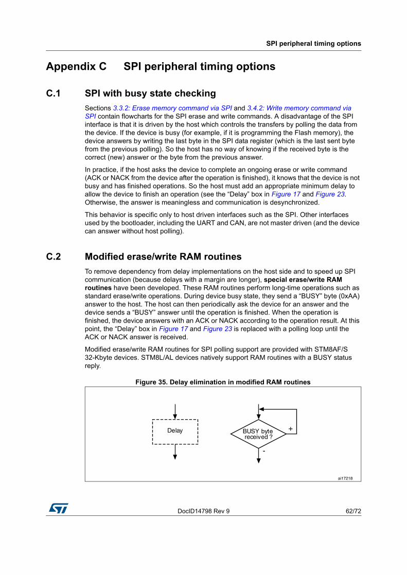
Sections 3.3.2: Erase memory command via SPI and 3.4.2: Write memory command via SPI contain flowcharts for the SPI erase and write commands. A disadvantage of the SPI interface is that it is driven by the host which controls the transfers by polling the data from the device. If the device is busy (for example, if it is programming the Flash memory), the device answers by writing the last byte in the SPI data register (which is the last sent byte from the previous polling). So the host has no way of knowing if the received byte is the correct (new) answer or the byte from the previous answer.
In practice, if the host asks the device to complete an ongoing erase or write command (ACK or NACK from the device after the operation is finished), it knows that the device is not busy and has finished operations. So the host must add an appropriate minimum delay to allow the device to finish an operation (see the “Delay” box in Figure 17 and Figure 23. Otherwise, the answer is meaningless and communication is desynchronized.
This behavior is specific only to host driven interfaces such as the SPI. Other interfaces used by the bootloader, including the UART and CAN, are not master driven (and the device can answer without host polling).
C.2 Modified erase/write RAM routines
To remove dependency from delay implementations on the host side and to speed up SPI communication (because delays with a margin are longer), special erase/write RAM routines have been developed. These RAM routines perform long-time operations such as standard erase/write operations. During device busy state, they send a “BUSY” byte (0xAA) answer to the host. The host can then periodically ask the device for an answer and the device sends a “BUSY” answer until the operation is finished. When the operation is finished, the device answers with an ACK or NACK according to the operation result. At this point, the “Delay” box in Figure 17 and Figure 23 is replaced with a polling loop until the ACK or NACK answer is received.
Modified erase/write RAM routines for SPI polling support are provided with STM8AF/S 32-Kbyte devices. STM8L/AL devices natively support RAM routines with a BUSY status reply.
Figure 35. Delay elimination in modified RAM routines
PC software support
63/72 DocID14798 Rev 9
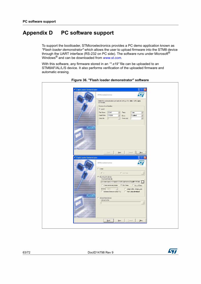
Appendix D PC software support
To support the bootloader, STMicroelectronics provides a PC demo application known as "Flash loader demonstrator" which allows the user to upload firmware into the STM8 device through the UART interface (RS-232 on PC side). The software runs under Microsoft® Windows® and can be downloaded from www.st.com.
With this software, any firmware stored in an “*.s19” file can be uploaded to an STM8AF/AL/L/S device. It also performs verification of the uploaded firmware and automatic erasing.
The bootloader limitation is not caused by a wrong bootloader implementation, or a non-compliance with specifications, but results from customer specific usage of the STM8 ROM bootloader.
To prevent future problems for occurring, use the workarounds that apply to your specific case (see Section E.2: Workaround for UART limitation).
E.1.1 UART automatic baudrate calculation
As explained in Section 2.1: USART/UARTs settings, the bootloader polls all peripherals (CAN, SPI, UART, SPI) waiting for a synchronization byte. The communications start when a synchronization byte equal to 0x7F has been received.
For UART communications, the baudrate at which UART data transfers are performed by the master is unknown whereas it is preknown for SPI communications, and fixed to 125 kbps for CAN.
Before initializing the UART interface, the bootloader waits for the 0x7F byte, and deduces the master baudrate from the speed at which the synchronization byte is sent. This is called the automatic baudrate mechanism. This is done by polling the RxD GPIO pin.
1. The master sends 0x7F in serial format (LSB first) through the UART interface. 0x7F is composed of:
– Start bit (‘0’)
– 7 consecutive logical 1s bits (LSB first)
– 1 logical ‘0’ (MSB bit of 0x7F)
– Even parity bit (‘1’)
– Stop bit (‘1’)
2. The bootloader polls the RxD pin and waits for the start bit (‘0’).
3. The bootloader starts the timer just after a rising edge has been detected on RxD (LSB bit) and measures the duration of the 7 logical 1s transmission.
4. The bootloader stops the timer when a falling edge is detected on RxD (end of 7 consecutive logical 1s – beginning of MSB). The number of timer ticks represents the duration the 7 logical 1s. The bootloader deduces the time required to transmit one bit by dividing the timer ticks by 7, calculates the baudrate, and initializes the UART baudrate accordingly. The bootloader is then ready to receive the next command from the master.
E.1.2 Description of UART limitation
Automatic baudrate calculation assumes that the master sends 0x7F as synchronization byte. However, the calculated baudrate is incorrect if the master sends a value different from 0x7F. This is due to fact that the bootloader expects 7 consecutive logical 1s after the start bit.
As an example, if the master sends 0x78 as synchronization byte, the start bit is followed by 4 consecutive logical 1s. Since the bootloader expects 7 consecutive 1s, the baudrate computed by the bootloader is 7/4 of the master baudrate. The next communication
Bootloader UART limitation
65/72 DocID14798 Rev 9
between master and bootloader fails due to indifferent baudrates, and the bootloader enters an endless loop waiting for valid master command. This state can only be exited by resetting the STM8 device.
The master must consequently send 0x7F after reset to launch the bootloader correctly or must sent nothing during 1 second after reset to avoid launching the bootloader and continue executing the user application. Any another byte sent to the bootloader up to 1 second after reset causes the bootloader to enter an endless loop.
This situation may occur in user application if the STM8 device is reset and huge data transfers are in progress through the UART interface. The device then enters an endless loop due to several synchronization byte reception.
E.2 Workaround for UART limitation
The issue described above can be fixed by using the workaround below.
This workaround consists in modifying your application code and the device configuration. It is recommended if your application is subject to enter an endless loop when starting UART communications. The following steps are required:
1. Disable the bootloader by using the option bytes (disabled on virgin devices).
2. Insert in your application code a routine that invokes the bootloader when a firmware upgrade is required, e.g. your code jumps to given bootloader entry point after pressing a button (see Appendix B: Bootloader entry points for details on entry point addresses).
As a result the bootloader is not active after reset and will not enter an endless loop when receiving random UART bytes. After reset the bootloader executes the application code without any delay, which is also a benefit for your application.
If an upgrade of the application code is required, follow the sequence below:
1. Press the button so that the code invokes the bootloader and jumps to a given bootloader entry point. You must make sure that a master device is connected to the UART interface and no random byte is sent.
2. Run the master to upgrade the code through the standard ROM bootloader.
3. Reset the device when the upgrade is complete.
Invoking the bootloader by pressing a button can be replaced by any similar action, e.g. receiving a specific command or an authentication password to launch an upgrade of the application code (only authenticated person can upgrade).
The programming operation might crash during code upgrade (for example when powering off the device). In this case, the bootloader cannot be entered again because the application code was not properly upgraded and is invalid. To prevent this issue from occurring, it is recommended that the master executes the following steps before entering the bootloader:
1. Enable the ROM bootloader through the option bytes before downloading the application code into device.
2. Download the application code and verify it.
3. Disable again the ROM bootloader by using the option bytes.
DocID14798 Rev 9 66/72
Limitations and improvements versus bootloader versions
71
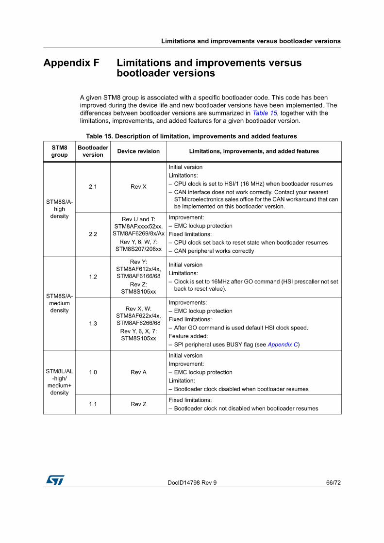
Appendix F Limitations and improvements versus bootloader versions
A given STM8 group is associated with a specific bootloader code. This code has been improved during the device life and new bootloader versions have been implemented. The differences between bootloader versions are summarized in Table 15, together with the limitations, improvements, and added features for a given bootloader version.
Table 15. Description of limitation, improvements and added features
STM8 group
Bootloader version
Device revision Limitations, improvements, and added features
STM8S/A-high
density
2.1 Rev X
Initial version
Limitations:
– CPU clock is set to HSI/1 (16 MHz) when bootloader resumes
– CAN interface does not work correctly. Contact your nearest STMicroelectronics sales office for the CAN workaround that can be implemented on this bootloader version.
2.2
Rev U and T: STM8AFxxxx52xx,
STM8AF6269/8x/Ax
Rev Y, 6, W, 7: STM8S207/208xx
Improvement:
– EMC lockup protection
Fixed limitations:
– CPU clock set back to reset state when bootloader resumes
– CAN peripheral works correctly
STM8S/A-medium density
1.2
Rev Y: STM8AF612x/4x, STM8AF6166/68
Rev Z: STM8S105xx
Initial version
Limitations:
– Clock is set to 16MHz after GO command (HSI prescaller not set back to reset value).
1.3
Rev X, W: STM8AF622x/4x, STM8AF6266/68
Rev Y, 6, X, 7: STM8S105xx
Improvements:
– EMC lockup protection
Fixed limitations:
– After GO command is used default HSI clock speed.
Feature added:
– SPI peripheral uses BUSY flag (see Appendix C)
STM8L/AL-high/
medium+ density
1.0 Rev A
Initial version
Improvement:
– EMC lockup protection
Limitation:
– Bootloader clock disabled when bootloader resumes
1.1 Rev ZFixed limitations:
– Bootloader clock not disabled when bootloader resumes
Limitations and improvements versus bootloader versions
67/72 DocID14798 Rev 9
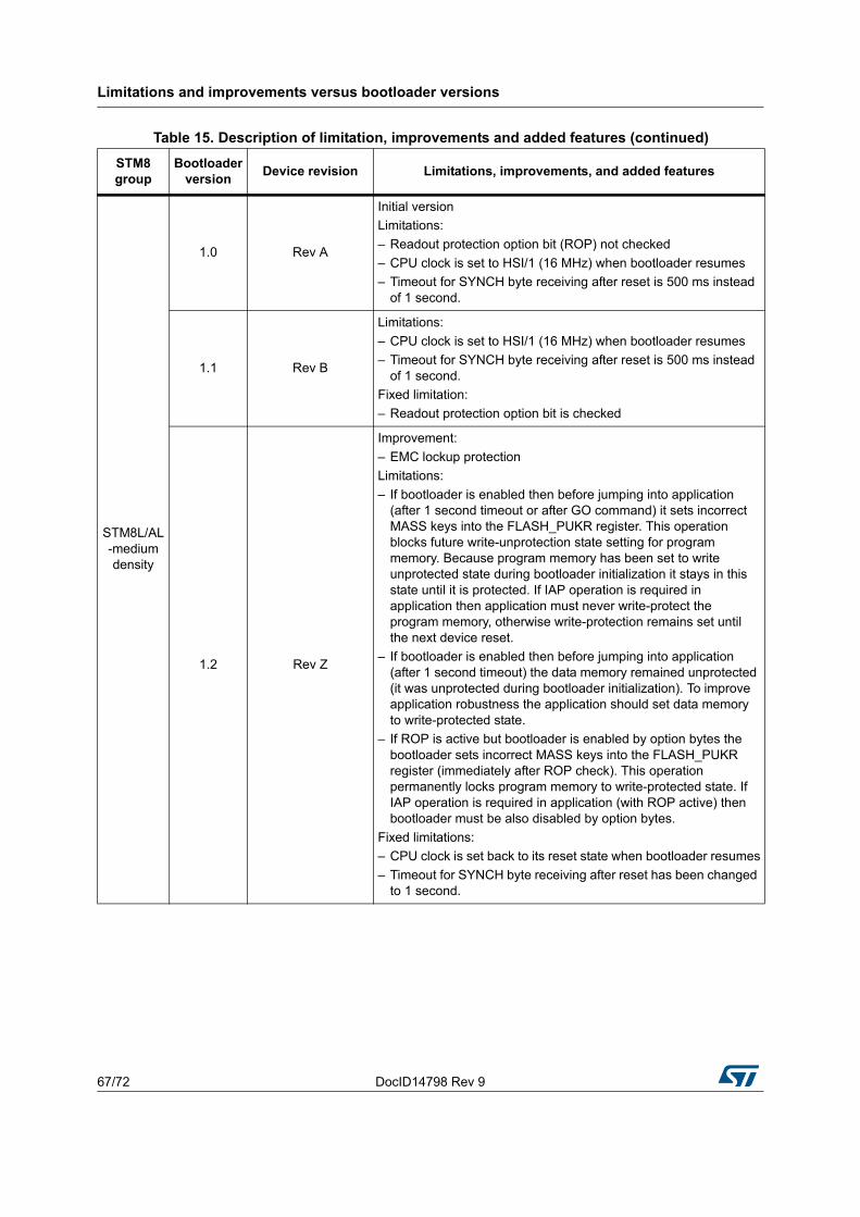
STM8L/AL-medium density
1.0 Rev A
Initial version
Limitations:
– Readout protection option bit (ROP) not checked
– CPU clock is set to HSI/1 (16 MHz) when bootloader resumes
– Timeout for SYNCH byte receiving after reset is 500 ms instead of 1 second.
1.1 Rev B
Limitations:
– CPU clock is set to HSI/1 (16 MHz) when bootloader resumes
– Timeout for SYNCH byte receiving after reset is 500 ms instead of 1 second.
Fixed limitation:
– Readout protection option bit is checked
1.2 Rev Z
Improvement:
– EMC lockup protection
Limitations:
– If bootloader is enabled then before jumping into application (after 1 second timeout or after GO command) it sets incorrect MASS keys into the FLASH_PUKR register. This operation blocks future write-unprotection state setting for program memory. Because program memory has been set to write unprotected state during bootloader initialization it stays in this state until it is protected. If IAP operation is required in application then application must never write-protect the program memory, otherwise write-protection remains set until the next device reset.
– If bootloader is enabled then before jumping into application (after 1 second timeout) the data memory remained unprotected (it was unprotected during bootloader initialization). To improve application robustness the application should set data memory to write-protected state.
– If ROP is active but bootloader is enabled by option bytes the bootloader sets incorrect MASS keys into the FLASH_PUKR register (immediately after ROP check). This operation permanently locks program memory to write-protected state. If IAP operation is required in application (with ROP active) then bootloader must be also disabled by option bytes.
Fixed limitations:
– CPU clock is set back to its reset state when bootloader resumes
– Timeout for SYNCH byte receiving after reset has been changed to 1 second.
Table 15. Description of limitation, improvements and added features (continued)
STM8 group
Bootloader version
Device revision Limitations, improvements, and added features
DocID14798 Rev 9 68/72
Limitations and improvements versus bootloader versions
71
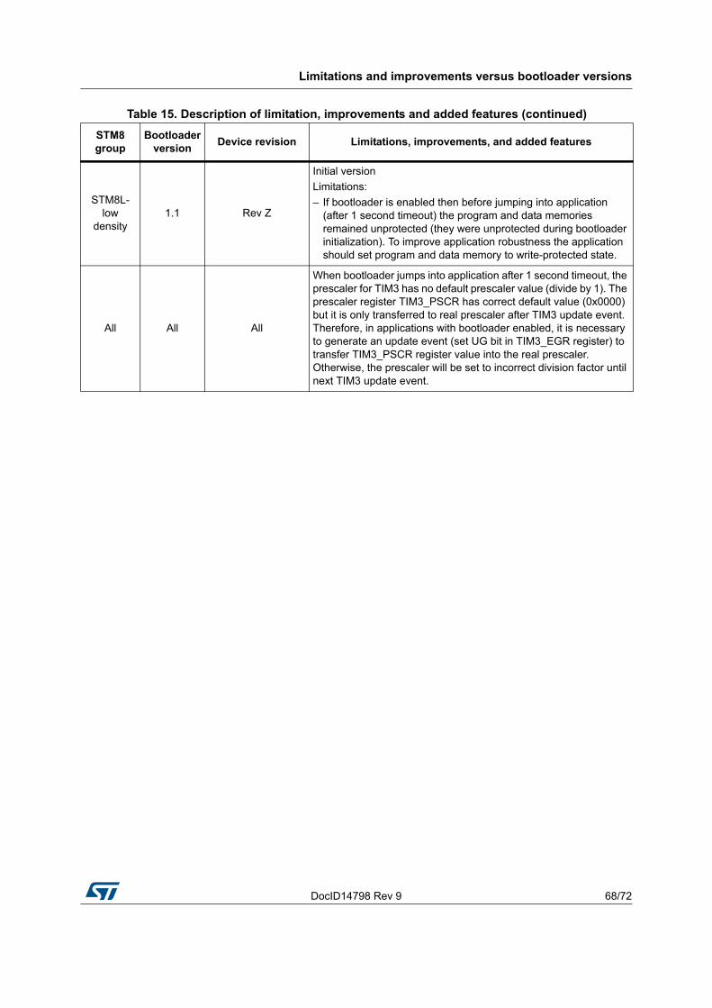
STM8L-low
density1.1 Rev Z
Initial version
Limitations:
– If bootloader is enabled then before jumping into application (after 1 second timeout) the program and data memories remained unprotected (they were unprotected during bootloader initialization). To improve application robustness the application should set program and data memory to write-protected state.
All All All
When bootloader jumps into application after 1 second timeout, the prescaler for TIM3 has no default prescaler value (divide by 1). The prescaler register TIM3_PSCR has correct default value (0x0000) but it is only transferred to real prescaler after TIM3 update event. Therefore, in applications with bootloader enabled, it is necessary to generate an update event (set UG bit in TIM3_EGR register) to transfer TIM3_PSCR register value into the real prescaler. Otherwise, the prescaler will be set to incorrect division factor until next TIM3 update event.
Table 15. Description of limitation, improvements and added features (continued)
STM8 group
Bootloader version
Device revision Limitations, improvements, and added features
Revision history
69/72 DocID14798 Rev 9
Revision history
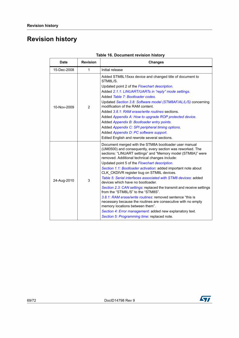
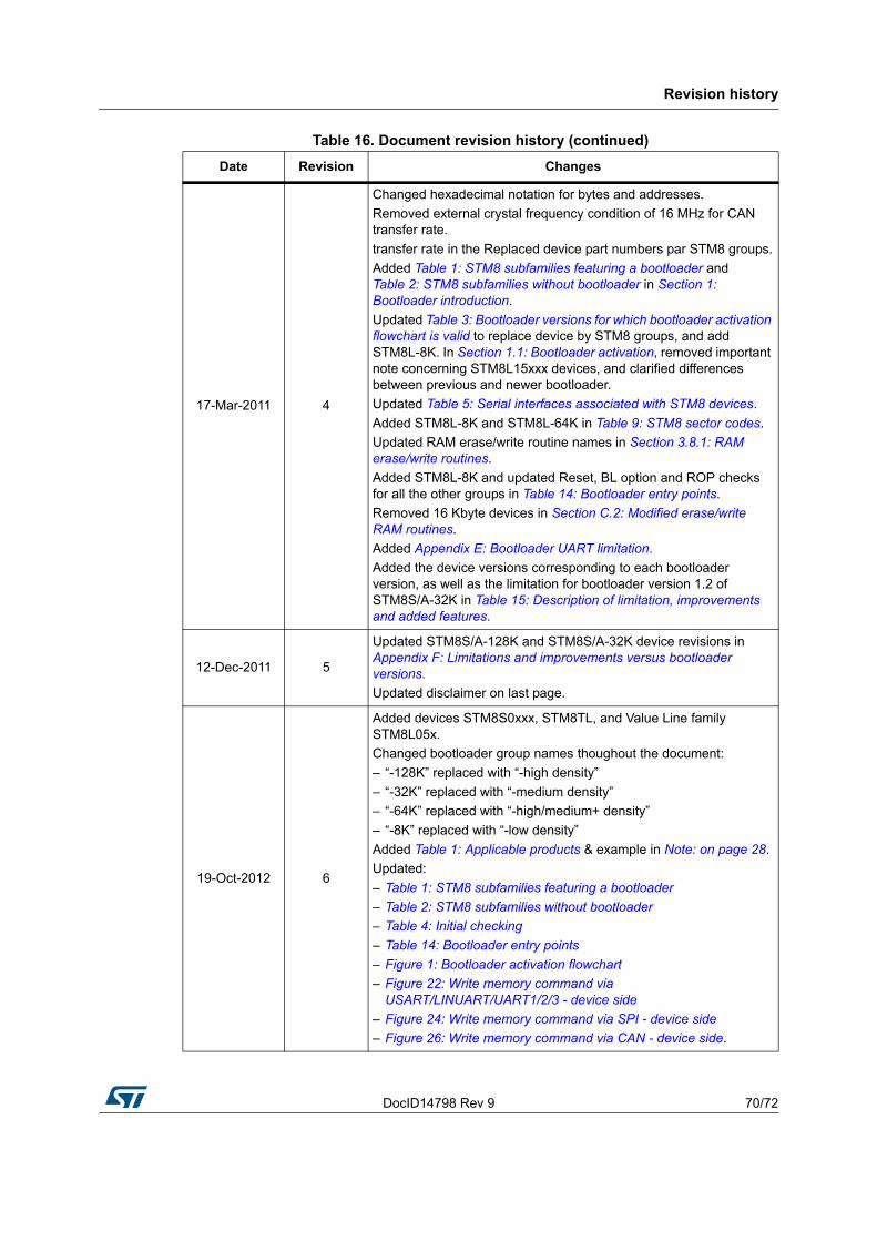
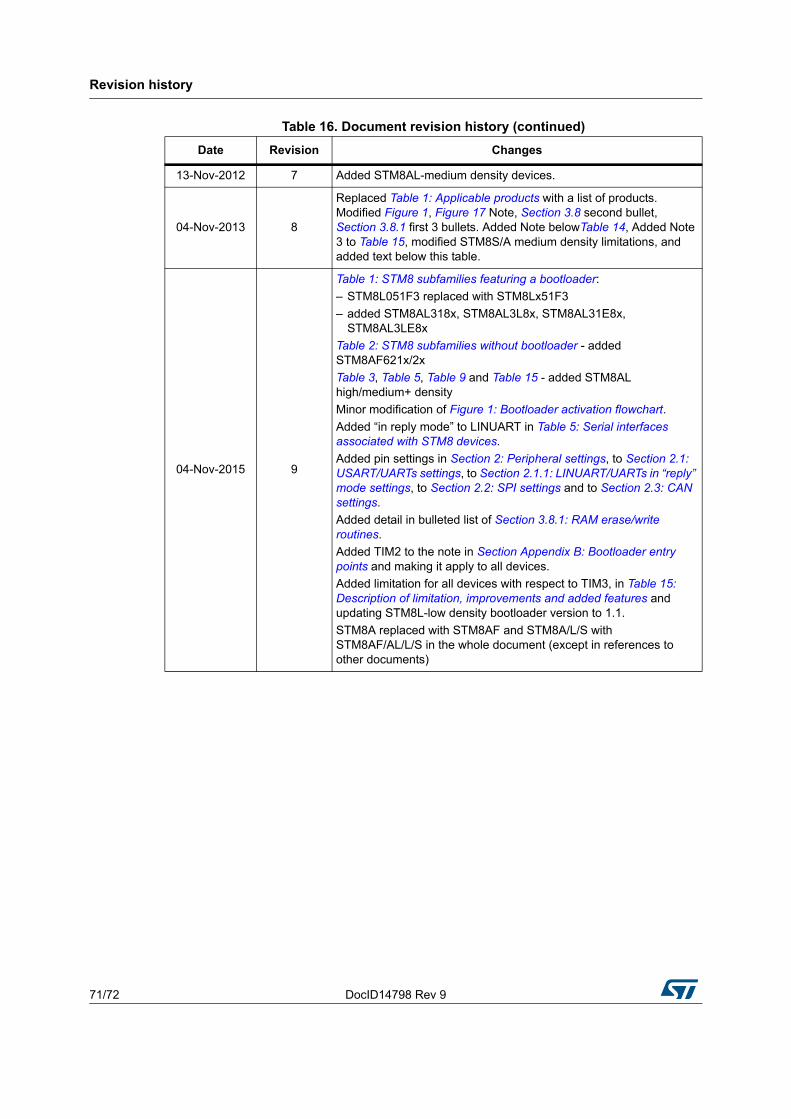
Table 16. Document revision history
Date Revision Changes
15-Dec-2008 1 Initial release
10-Nov-2009 2
Added STM8L15xxx device and changed title of document to STM8L/S.
Updated point 2 of the Flowchart description.
Added 2.1.1: LINUART/UARTs in “reply” mode settings.
Added Table 7: Bootloader codes.
Updated Section 3.8: Software model (STM8AF/AL/L/S) concerning modification of the RAM content.
Added 3.8.1: RAM erase/write routines sections.
Added Appendix A: How to upgrade ROP protected device.
Added Appendix B: Bootloader entry points.
Added Appendix C: SPI peripheral timing options.
Added Appendix D: PC software support.
Edited English and rewrote several sections.
24-Aug-2010 3
Document merged with the STM8A bootloader user manual (UM0500) and consequently, every section was reworked. The sections: “LINUART settings” and “Memory model (STM8A)” were removed. Additional technical changes include:
Updated point 5 of the Flowchart description.
Section 1.1: Bootloader activation: added important note about CLK_CKDIVR register bug on STM8L devices.
Table 5: Serial interfaces associated with STM8 devices: added devices which have no bootloader.
Section 2.3: CAN settings: replaced the transmit and receive settings from the “STM8L/S” to the “STM8S”.
3.8.1: RAM erase/write routines: removed sentence “this is necessary because the routines are consecutive with no empty memory locations between them”.
Section 4: Error management: added new explanatory text.
Section 5: Programming time: replaced note.
DocID14798 Rev 9 70/72
Revision history
71
17-Mar-2011 4
Changed hexadecimal notation for bytes and addresses.
Removed external crystal frequency condition of 16 MHz for CAN transfer rate.
transfer rate in the Replaced device part numbers par STM8 groups.
Added Table 1: STM8 subfamilies featuring a bootloader and Table 2: STM8 subfamilies without bootloader in Section 1: Bootloader introduction.
Updated Table 3: Bootloader versions for which bootloader activation flowchart is valid to replace device by STM8 groups, and add STM8L-8K. In Section 1.1: Bootloader activation, removed important note concerning STM8L15xxx devices, and clarified differences between previous and newer bootloader.
Updated Table 5: Serial interfaces associated with STM8 devices.
Added STM8L-8K and STM8L-64K in Table 9: STM8 sector codes.
Added the device versions corresponding to each bootloader version, as well as the limitation for bootloader version 1.2 of STM8S/A-32K in Table 15: Description of limitation, improvements and added features.
12-Dec-2011 5
Updated STM8S/A-128K and STM8S/A-32K device revisions in Appendix F: Limitations and improvements versus bootloader versions.
Updated disclaimer on last page.
19-Oct-2012 6
Added devices STM8S0xxx, STM8TL, and Value Line family STM8L05x.
Changed bootloader group names thoughout the document:
– “-128K” replaced with “-high density”
– “-32K” replaced with “-medium density”
– “-64K” replaced with “-high/medium+ density”
– “-8K” replaced with “-low density”
Added Table 1: Applicable products & example in Note: on page 28.
Updated:
– Table 1: STM8 subfamilies featuring a bootloader
– Table 2: STM8 subfamilies without bootloader
– Table 4: Initial checking
– Table 14: Bootloader entry points
– Figure 1: Bootloader activation flowchart
– Figure 22: Write memory command via USART/LINUART/UART1/2/3 - device side
– Figure 24: Write memory command via SPI - device side
– Figure 26: Write memory command via CAN - device side.
Table 16. Document revision history (continued)
Date Revision Changes
Revision history
71/72 DocID14798 Rev 9
13-Nov-2012 7 Added STM8AL-medium density devices.
04-Nov-2013 8
Replaced Table 1: Applicable products with a list of products. Modified Figure 1, Figure 17 Note, Section 3.8 second bullet, Section 3.8.1 first 3 bullets. Added Note belowTable 14, Added Note 3 to Table 15, modified STM8S/A medium density limitations, and added text below this table.
Table 2: STM8 subfamilies without bootloader - added STM8AF621x/2x
Table 3, Table 5, Table 9 and Table 15 - added STM8AL high/medium+ density
Minor modification of Figure 1: Bootloader activation flowchart.
Added “in reply mode” to LINUART in Table 5: Serial interfaces associated with STM8 devices.
Added pin settings in Section 2: Peripheral settings, to Section 2.1: USART/UARTs settings, to Section 2.1.1: LINUART/UARTs in “reply” mode settings, to Section 2.2: SPI settings and to Section 2.3: CAN settings.
Added detail in bulleted list of Section 3.8.1: RAM erase/write routines.
Added TIM2 to the note in Section Appendix B: Bootloader entry points and making it apply to all devices.
Added limitation for all devices with respect to TIM3, in Table 15: Description of limitation, improvements and added features and updating STM8L-low density bootloader version to 1.1.
STM8A replaced with STM8AF and STM8A/L/S with STM8AF/AL/L/S in the whole document (except in references to other documents)
Table 16. Document revision history (continued)
Date Revision Changes
DocID14798 Rev 9 72/72
72
Please Read Carefully:
Information in this document is provided solely in connection with ST products. STMicroelectronics NV and its subsidiaries (“ST”) reserve theright to make changes, corrections, modifications or improvements, to this document, and the products and services described herein at anytime, without notice.
All ST products are sold pursuant to ST’s terms and conditions of sale.
Purchasers are solely responsible for the choice, selection and use of the ST products and services described herein, and ST assumes noliability whatsoever relating to the choice, selection or use of the ST products and services described herein.
No license, express or implied, by estoppel or otherwise, to any intellectual property rights is granted under this document. If any part of thisdocument refers to any third party products or services it shall not be deemed a license grant by ST for the use of such third party productsor services, or any intellectual property contained therein or considered as a warranty covering the use in any manner whatsoever of suchthird party products or services or any intellectual property contained therein.
UNLESS OTHERWISE SET FORTH IN ST’S TERMS AND CONDITIONS OF SALE ST DISCLAIMS ANY EXPRESS OR IMPLIEDWARRANTY WITH RESPECT TO THE USE AND/OR SALE OF ST PRODUCTS INCLUDING WITHOUT LIMITATION IMPLIEDWARRANTIES OF MERCHANTABILITY, FITNESS FOR A PARTICULAR PURPOSE (AND THEIR EQUIVALENTS UNDER THE LAWSOF ANY JURISDICTION), OR INFRINGEMENT OF ANY PATENT, COPYRIGHT OR OTHER INTELLECTUAL PROPERTY RIGHT.
ST PRODUCTS ARE NOT DESIGNED OR AUTHORIZED FOR USE IN: (A) SAFETY CRITICAL APPLICATIONS SUCH AS LIFESUPPORTING, ACTIVE IMPLANTED DEVICES OR SYSTEMS WITH PRODUCT FUNCTIONAL SAFETY REQUIREMENTS; (B)AERONAUTIC APPLICATIONS; (C) AUTOMOTIVE APPLICATIONS OR ENVIRONMENTS, AND/OR (D) AEROSPACE APPLICATIONSOR ENVIRONMENTS. WHERE ST PRODUCTS ARE NOT DESIGNED FOR SUCH USE, THE PURCHASER SHALL USE PRODUCTS ATPURCHASER’S SOLE RISK, EVEN IF ST HAS BEEN INFORMED IN WRITING OF SUCH USAGE, UNLESS A PRODUCT ISEXPRESSLY DESIGNATED BY ST AS BEING INTENDED FOR “AUTOMOTIVE, AUTOMOTIVE SAFETY OR MEDICAL” INDUSTRYDOMAINS ACCORDING TO ST PRODUCT DESIGN SPECIFICATIONS. PRODUCTS FORMALLY ESCC, QML OR JAN QUALIFIED AREDEEMED SUITABLE FOR USE IN AEROSPACE BY THE CORRESPONDING GOVERNMENTAL AGENCY.
Resale of ST products with provisions different from the statements and/or technical features set forth in this document shall immediately voidany warranty granted by ST for the ST product or service described herein and shall not create or extend in any manner whatsoever, anyliability of ST.
ST and the ST logo are trademarks or registered trademarks of ST in various countries.Information in this document supersedes and replaces all information previously supplied.
The ST logo is a registered trademark of STMicroelectronics. All other names are the property of their respective owners.
Australia - Belgium - Brazil - Canada - China - Czech Republic - Finland - France - Germany - Hong Kong - India - Israel - Italy - Japan - Malaysia - Malta - Morocco - Philippines - Singapore - Spain - Sweden - Switzerland - United Kingdom - United States of America