Emilio Fazzoletto - Analog and TLC Electronics - 2015 Pag. 1 STMicroelectronics Spirit1 Radio Module Overview, power consumption and integration Analog and TLC Electronics Prof: Dante Del Corso Student: Emilio Fazzoletto
Transcript
Emilio Fazzoletto - Analog and TLC Electronics - 2015 Pag. 1
STMicroelectronics Spirit1 Radio Module
Overview, power consumption and integration
Analog and TLC Electronics
Prof: Dante Del Corso
Student: Emilio Fazzoletto
2
Summary
Chapter 1: ST Microelectronics Spirit1 Module ........................................................................... 4
1.2.2 Transmission and Reception ............................................................................................................. 7
1.2.3 Data Modes ...................................................................................................................................... 9
1.3 Power Output Configuration and Supported Modulations ..................................................................... 9
1.3.1 Power Output Configuration ............................................................................................................ 9
Chapter 3: Power Consumption Characterization ..................................................................... 21
3.1 MCU in Standby Mode........................................................................................................................... 24
3.2 System battery life simulation ............................................................................................................... 25
Chapter 4: design of a PCB integrating the Spirit1 module ......................................................... 27
3
4.1 Idea ........................................................................................................................................................ 27
4.2 System Block Diagram ........................................................................................................................... 27
4.3 Schematic and PCB development .......................................................................................................... 28
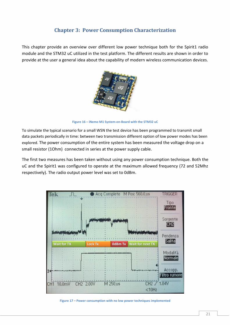
The current absorbed during idle has dropped from 34 to only 15mA for the entire system.
24
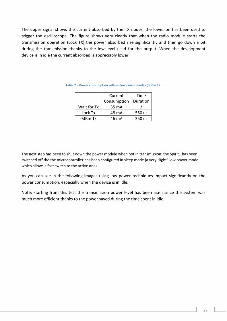
3.1 MCU in Standby Mode An further step is to use a deeper sleep mode for the MCU: in this case the standby mode for the STM32
was used. Using the standby mode the device can achieve much lower level of absorbed current even if it
will need a reconfiguration after the wake-up and this imply a much longer delay before restart the
operation. However, if the idle time is order of magnitude greater than the activity time, the standby mode
is undoubtedly a better solution.
To wake-up the MCU the RTC alarm interrupt has been used: in this way no external interrupt is
necessary, all the peripherals can be switched off except the LSI (Low-Speed Internal) oscillator in
order to minimize the power consumption.
Wait for TX Wait for TX Wait for TX Wait for TX
Figure 19 MCU Standby Mode
Current Consumption
Idle Period
MCU Sleep MCU Standby
15 mA 1,735 mA
25
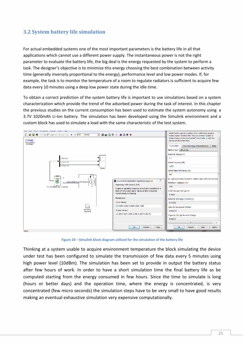
3.2 System battery life simulation
For actual embedded systems one of the most important parameters is the battery life in all that
applications which cannot use a different power supply. The instantaneous power is not the right
parameter to evaluate the battery life, the big deal is the energy requested by the system to perform a
task. The designer’s objective is to minimize this energy choosing the best combination between activity
time (generally inversely proportional to the energy), performance level and low power modes. If, for
example, the task is to monitor the temperature of a room to regulate radiators is sufficient to acquire few
data every 10 minutes using a deep low power state during the idle time.
To obtain a correct prediction of the system battery life is important to use simulations based on a system
characterization which provide the trend of the adsorbed power during the task of interest. In this chapter
the previous studies on the current consumption has been used to estimate the system autonomy using a
3.7V 1020mAh Li-Ion battery. The simulation has been developed using the Simulink environment and a
custom block has used to simulate a load with the same characteristic of the test system.
Figure 20 – Simulink block diagram utilized for the simulation of the battery life
Thinking at a system usable to acquire environment temperature the block simulating the device
under test has been configured to simulate the transmission of few data every 5 minutes using
high power level (10dBm). The simulation has been set to provide in output the battery status
after few hours of work. In order to have a short simulation time the final battery life as be
computed starting from the energy consumed in few hours. Since the time to simulate is long
(hours or better days) and the operation time, where the energy is concentrated, is very
concentrated (few micro seconds) the simulation steps have to be very small to have good results
making an eventual exhaustive simulation very expensive computationally.
26
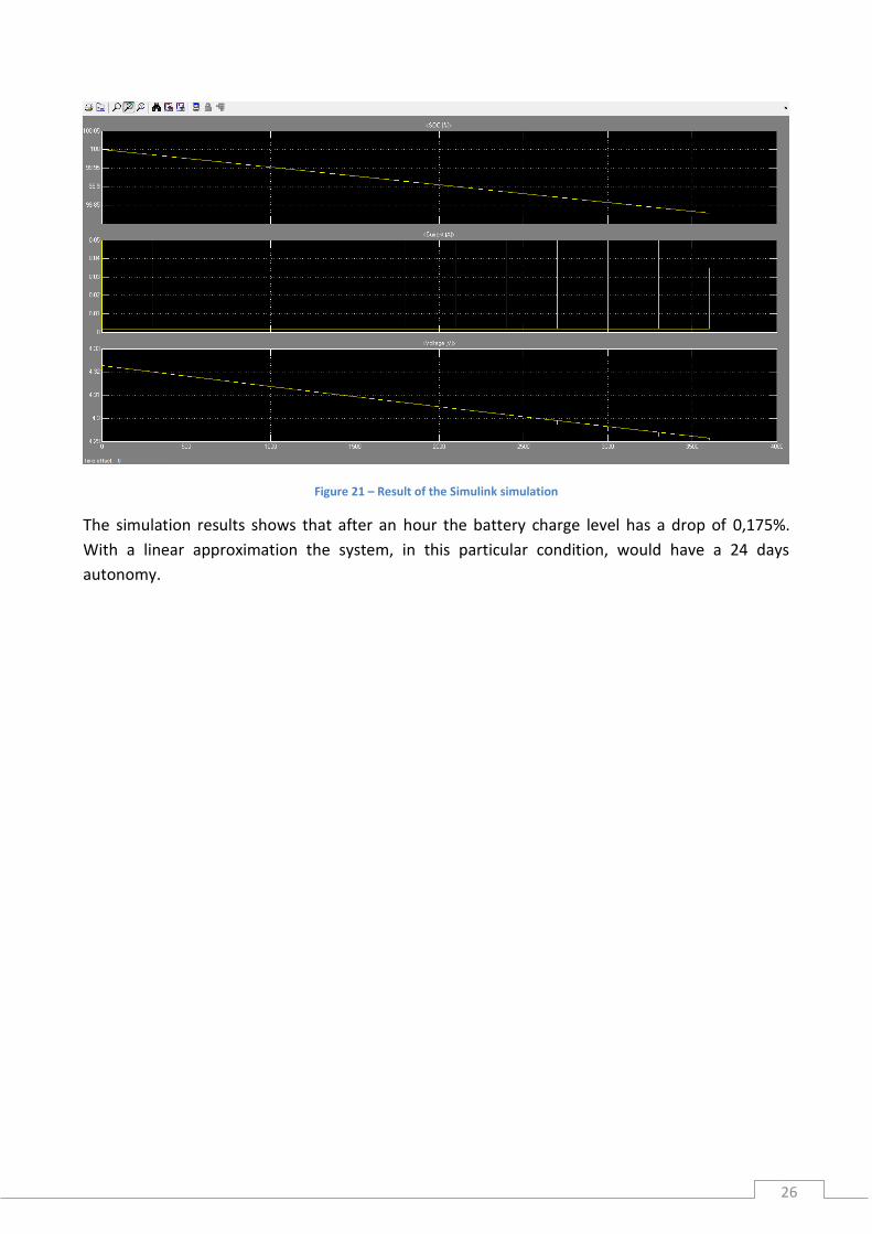
Figure 21 – Result of the Simulink simulation
The simulation results shows that after an hour the battery charge level has a drop of 0,175%.
With a linear approximation the system, in this particular condition, would have a 24 days
autonomy.
27
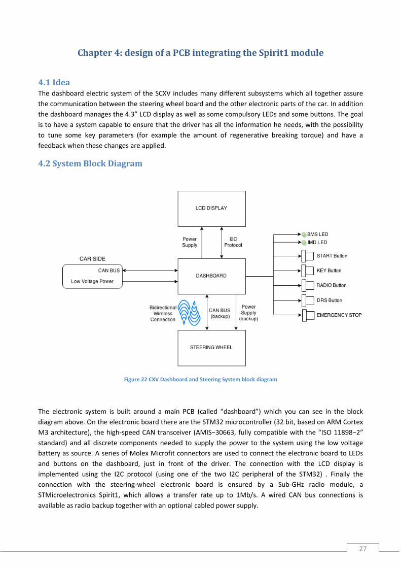
Chapter 4: design of a PCB integrating the Spirit1 module
4.1 Idea The dashboard electric system of the SCXV includes many different subsystems which all together assure
the communication between the steering wheel board and the other electronic parts of the car. In addition
the dashboard manages the 4.3” LCD display as well as some compulsory LEDs and some buttons. The goal
is to have a system capable to ensure that the driver has all the information he needs, with the possibility
to tune some key parameters (for example the amount of regenerative breaking torque) and have a
feedback when these changes are applied.
4.2 System Block Diagram
Figure 22 CXV Dashboard and Steering System block diagram
The electronic system is built around a main PCB (called “dashboard”) which you can see in the block
diagram above. On the electronic board there are the STM32 microcontroller (32 bit, based on ARM Cortex
M3 architecture), the high-speed CAN transceiver (AMIS−30663, fully compatible with the “ISO 11898−2”
standard) and all discrete components needed to supply the power to the system using the low voltage
battery as source. A series of Molex Microfit connectors are used to connect the electronic board to LEDs
and buttons on the dashboard, just in front of the driver. The connection with the LCD display is
implemented using the I2C protocol (using one of the two I2C peripheral of the STM32) . Finally the
connection with the steering-wheel electronic board is ensured by a Sub-GHz radio module, a
STMicroelectronics Spirit1, which allows a transfer rate up to 1Mb/s. A wired CAN bus connections is
available as radio backup together with an optional cabled power supply.
28
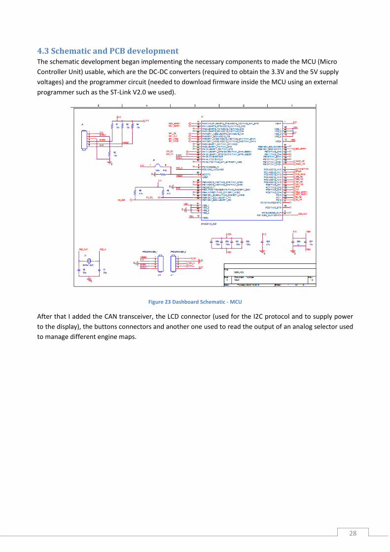
4.3 Schematic and PCB development The schematic development began implementing the necessary components to made the MCU (Micro
Controller Unit) usable, which are the DC-DC converters (required to obtain the 3.3V and the 5V supply
voltages) and the programmer circuit (needed to download firmware inside the MCU using an external
programmer such as the ST-Link V2.0 we used).
Figure 23 Dashboard Schematic - MCU
After that I added the CAN transceiver, the LCD connector (used for the I2C protocol and to supply power
to the display), the buttons connectors and another one used to read the output of an analog selector used
to manage different engine maps.
29
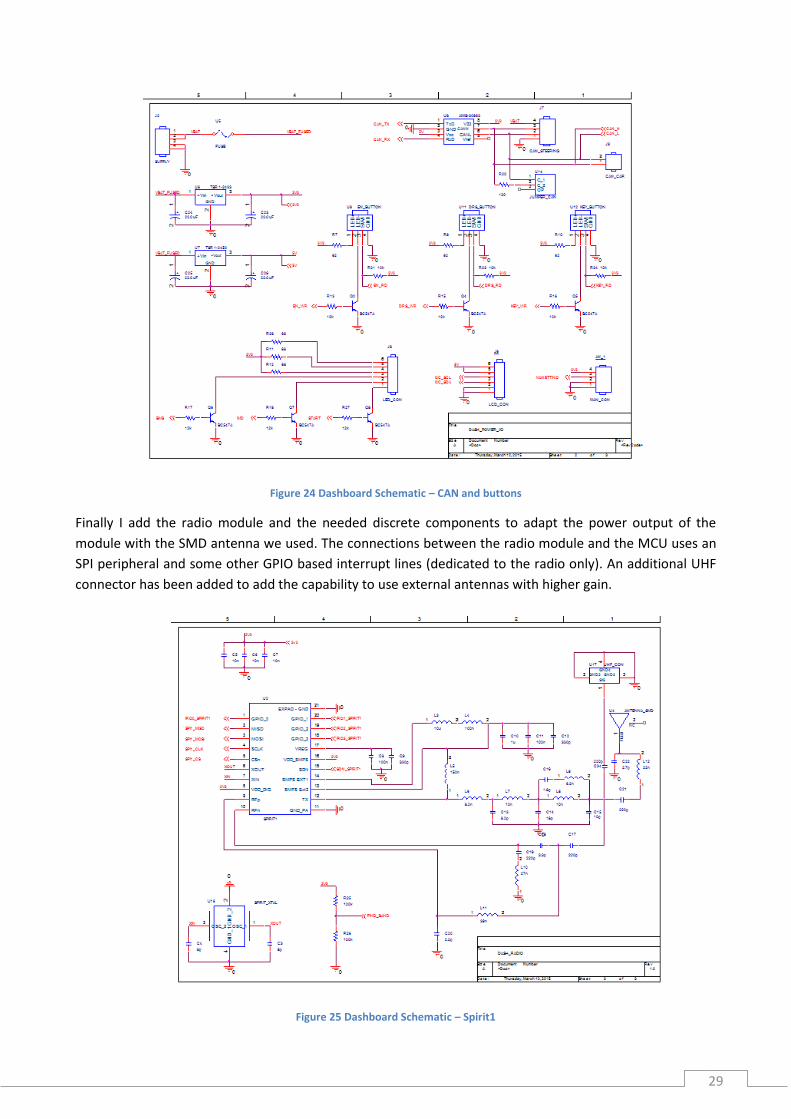
Figure 24 Dashboard Schematic – CAN and buttons
Finally I add the radio module and the needed discrete components to adapt the power output of the
module with the SMD antenna we used. The connections between the radio module and the MCU uses an
SPI peripheral and some other GPIO based interrupt lines (dedicated to the radio only). An additional UHF
connector has been added to add the capability to use external antennas with higher gain.
Figure 25 Dashboard Schematic – Spirit1
30
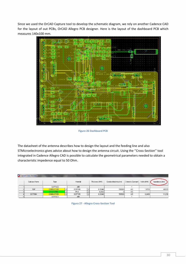
Since we used the OrCAD Capture tool to develop the schematic diagram, we rely on another Cadence CAD
for the layout of out PCBs, OrCAD Allegro PCB designer. Here is the layout of the dashboard PCB which
measures 140x100 mm.
Figure 26 Dashboard PCB
The datasheet of the antenna describes how to design the layout and the feeding line and also
STMicroelectronics gives advice about how to design the antenna circuit. Using the ‘’Cross-Section’’ tool
integrated in Cadence Allegro CAD is possible to calculate the geometrical parameters needed to obtain a
characteristic impedence equal to 50 Ohm.
Figura 27 - Allegro Cross-Section Tool
31
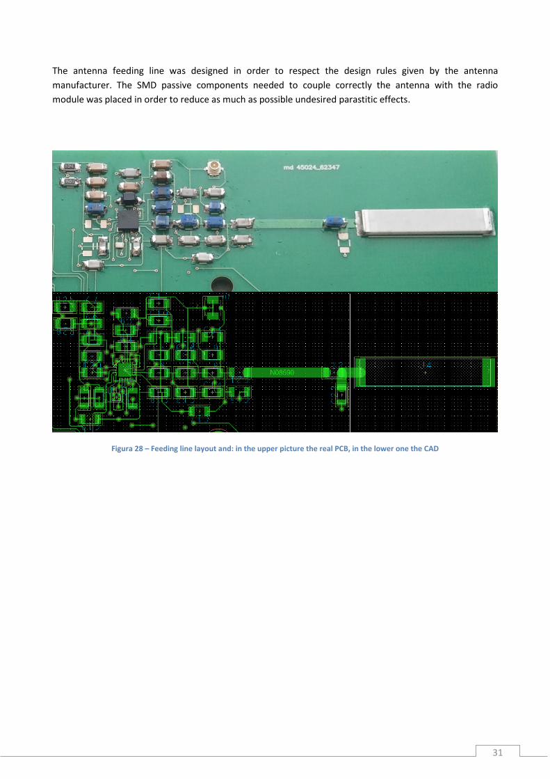
The antenna feeding line was designed in order to respect the design rules given by the antenna
manufacturer. The SMD passive components needed to couple correctly the antenna with the radio
module was placed in order to reduce as much as possible undesired parastitic effects.
Figura 28 – Feeding line layout and: in the upper picture the real PCB, in the lower one the CAD
32
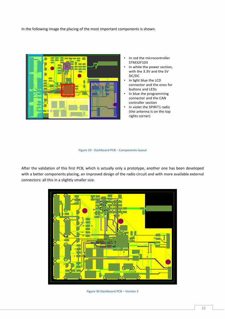
In the following image the placing of the most important components is shown.
• In red the microcontrollerSTM32F103
• In white the power section, with the 3.3V and the 5V DC/DC
• In light blue the LCD connector and the ones for buttons and LEDs
• In blue the programmingconnector and the CAN controller section
• In violet the SPIRIT1 radio (the antenna is on the top rights corner)
Figure 29 - Dashboard PCB – Components layout
After the validation of this first PCB, which is actually only a prototype, another one has been developed
with a better components placing, an improved design of the radio circuit and with more available external
connectors: all this in a slightly smaller size.
Figure 30 Dashboard PCB – Version 2
33
References
“STM32F103xE” Datasheet, Doc ID 14611 Rev 7, 2009
“STM32F103xx” Reference Manual, Doc ID 13902 Rev 14, 2011
“Spirit1 Low data rate, low power sub-1GHZ transceiver” Datasheet, DocID022758 Rev 5, 2013
Mihail L. Sichitiu and Chanchai Veerarittiphan, “Simple, Accurate Time Synchronization for Wireless Sensor Networks”, IEEE Wireless Communication and Networking, 2003, vol 2., pp. 1266-1273
“How to achieve the lowest current consumption with STM32F2xx” Application Note, Doc ID 019009 Rev 1, 2011
“Using the STM32 hardware real-time clock (RTC)” Application Note, Doc ID 018624 Rev 2, 2011
Dae-cheol You, Young-Si Hwang, Young-Ho Ahn, Ki-Seok Chung, “Energy Consumption Prediction Technique for Embedded Mobile Device by Using Battery Discharging Pattern”, Network Infrastructure and Digital Content, IEEE International Conference, 2010
“STM32 Nucleo boards” User Manual, DocID025833 Rev 2, 2014
“STM32L151xE and STM32L152xE” Datasheet, DocID025433 Rev 3, 2014


![Guidelines for Battery Operated applications with SPIRIT1 · Title: Guidelines for Battery operated applications with SPIRIT1 v10 [Read-Only] Author: giacomo timpanaro Created Date:](https://static.documents.pub/doc/80x56/5c71262b09d3f2e7398c32a0/guidelines-for-battery-operated-applications-with-title-guidelines-for-battery.jpg)

