Stretchable and transparent electrodes based onin-plane structures
Kukjoo Kim, Joohee Kim, Byung Gwan Hyun, Sangyoon Ji, So-Yun Kim,Sungwon Kim, Byeong Wan An and Jang-Ung Park*
Stretchable electronics has attracted great interest with compelling potential applications that require
reliable operation under mechanical deformation. Achieving stretchability in devices, however, requires a
deeper understanding of nanoscale materials and mechanics beyond the success of flexible electronics.
In this regard, tremendous research efforts have been dedicated toward developing stretchable electro-
des, which are one of the most important building blocks for stretchable electronics. Stretchable trans-
parent thin-film electrodes, which retain their electrical conductivity and optical transparency under
mechanical deformation, are particularly important for the favourable application of stretchable devices.
This minireview summarizes recent advances in stretchable transparent thin-film electrodes, especially
employing strategies based on in-plane structures. Various approaches using metal nanomaterials, carbon
nanomaterials, and their hybrids are described in terms of preparation processes and their optoelectronic/
mechanical properties. Some challenges and perspectives for further advances in stretchable transparent
electrodes are also discussed.
1. Introduction
Beyond the concept of conventional appliances, electronics israpidly evolving toward a new paradigm of deformable elec-tronics, where electronic devices can be deformed into variousshapes. Stretchable electronics, in particular, is the most soph-isticated form of deformable electronics in that it involvesstate-of-the-art technologies developed through the collabor-ation of various disciplines, ranging from materials science toelectrical and mechanical engineering.1–3 Potential productsemploying stretchable electronics exhibit unprecedentedattractive applications that strongly appeal to users. Typicalexamples include wearable healthcare devices, artificial skinand muscles, human–machine interfaces, stretchable displays,and stretchable batteries.4–10
As well described in some excellent previous reports,1,11,12
stretchable conductors, among various components, are oneof the most important building blocks of stretchable elec-tronics because electrodes and interconnects occupy a verylarge area portion of electronic devices, thereby absorbingmost of the externally induced physical strains. Impartingoptical transparency to stretchable electrodes is particularlyimportant for the realization of stretchable optoelectronics,
such as stretchable displays,9,13 photovoltaics,14 touch panels,15
and smart contact lenses.16 However, maintaining acceptableelectrical and optical performances under mechanical elonga-tion is not readily achieved even with flexible electrodesbecause a higher level of deformation is required for stretchingor twisting than for bending. Therefore, extensive efforts havebeen recently dedicated to discovering alternative stretchabletransparent electrodes beyond flexible transparent electrodes.In most cases, the stretchability of transparent electrodes isrendered by certain structural configurations rather than byexploiting intrinsic properties of materials. Generally, thesestructural configurations include out-of-plane and in-planestructures of conducting materials. Three-dimensional wavy,crumpled, or coiled shapes are examples of the out-of-planestructure, whereas two-dimensional percolation networks andmesh-like geometries belong to the in-plane structure.
In this mini review, we focus specifically on stretchabletransparent thin-film electrodes based on in-plane configur-ations. In section 2, we compare two distinctive strategies (i.e.,out-of-plane and in-plane structure-based approaches) for therealization of stretchable transparent electrodes. Graphene-and conducting polymer-based electrodes are described tocompare the two above-mentioned strategies. In sections 3–5,we elucidate the recent advances in stretchable transparentelectrodes based on metal nanowires, metal nanomeshes,carbon nanotubes (CNTs), and some other unique approaches.Lastly, in section 6, we discuss present challenges and futuredirections for stretchable transparent electrodes.
School of Materials Science and Engineering, Wearable Electronics Research Group,
Low-Dimensional Carbon Materials Research Center, Ulsan National Institute of
Science and Technology (UNIST), Ulsan 689-798, Republic of Korea.
2. Approaches based on out-of-planeor in-plane structures
Stretchability of transparent electrodes is usually achieved bystructural configurations that accommodate most of the strainunder mechanical deformation, thereby rendering little strainto the conducting material itself. These structural configur-ations can be classified into two approaches: out-of-plane andin-plane structures. The most common out-of-plane structureis the ‘wavy’ structure. The wavy structures can be generallyobtained by depositing conductive materials on pre-strainedelastomeric substrates, which are subsequently released toallow those conductive films to spontaneously form periodicwavy structures (Fig. 1a).17–19 In this wavy structure, most ofthe induced strain is absorbed by structural changes (i.e.,increased buckling wavelengths and decreased buckling ampli-tudes), which is similar to accordion bellows. In addition tothe simple wavy structures, some other out-of-plane structureshave been explored as well, including coiled or spring-likestructures.20,21
Graphene is a good example of a stretchable transparentelectrode with out-of-plane configuration. Graphene hassuperior properties, such as high charge carrier mobility,mechanical robustness, chemical stability, and optical trans-parency and therefore has been investigated in numerousresearch areas.22–25 Because graphene can be synthesized onlarge-area templates26 and transferred onto specific sub-strates,27 many applications have been reported utilizing gra-phene as electrodes for transistors, supercapacitors, anddisplays.11 Various flexible devices exploiting the flexibility ofgraphene have also been demonstrated.28–30 However, despitethe superb flexibility of graphene, a stretching-induced tensilestrain over 6% causes mechanical failure of graphene due tothe fractures within the unique honeycomb structure.27 Thus,the stretchability of graphene electrodes is usually achieved byimparting some structural configurations to graphene films.Recent studies revealed that wrinkled31 or crumpled7 graphene(i.e., graphene films with out-of-plane structures) can enduremechanical deformation, such as bending, distortion, andstretching. Chen et al.31 introduced wrinkled graphene syn-thesized on a wavy Cu template, showing that wrinkled gra-phene is able to maintain electrical performances under astrain of up to 40%. Zang et al.7 reported crumpled grapheneprepared by transferring graphene onto a polydimethylsiloxane(PDMS) substrate with a pre-strain (εpre) of 400%, followed bythe release of the pre-strained elastomer. This crumpled gra-phene sustained acceptable electrical properties duringrepeated stretching up to the level of the pre-strain. Such out-of-plane structured graphene films were applied to super-capacitors31 and artificial-muscle actuators.7 We observed thesurface morphology change of a wrinkled graphene film,which was deposited on a pre-strained PDMS substrate (εpre =10%), upon stretching and releasing, as shown in Fig. 1b. Asthe film stretches from the released state to the fully stretchedstate (ε = 10%), the film flattens out, becoming almost comple-
tely flat at 10% stretching. The graphene film recovers itswrinkled structure upon releasing. This structural changedepending on the degree of stretching induces variations inoptical transmittance due to light scattering on the surface(the bottom left plot of Fig. 1b), which is unfavourable fortransparent electrode applications. Zang et al.7 also reporteddecreasing transmittance of the crumpled graphene electrodeas the pre-strained substrate is released, as shown in Fig. 1c.
Similar to graphene, stretchable transparent electrodesusing poly(3,4-ethylenedioxythiophene):poly(styrenesulfonate)(PEDOT:PSS), a representative conducting polymer, have beendemonstrated by applying out-of-plane structures to PEDOT:PSS layers. Although PEDOT:PSS has been considered as apromising material for optoelectronics due to its low-cost pro-cessability via solution processes, a limited strain sustainabil-ity (<5%)32 restricts its use for stretchable electronics withoutthe aid of structural configurations. Lipomi et al.14 successfullydemonstrated a stretchable transparent PEDOT:PSS electrodefor organic photovoltaics (OPVs) with a buckling structure. Theresulting PEDOT:PSS electrode, made on a pre-strained elasto-meric substrate, exhibited a stretchability of 20% (up to thepre-strain) with a sheet resistance of 750 Ω sq−1 and transmit-tance of 96%. Vosgueritchian et al.33 described the use ofZonyl fluorosurfactant to enhance the processability and elec-trical conductivity of PEDOT:PSS through controlled wettabilityand phase segregation. A stretchable transparent electrode wasfabricated by spin-coating the mixed solution on a pre-strainedPDMS substrate (εpre = 15%) and subsequent releasing, provid-ing buckles or waves (Fig. 1d). The resulting electrode showeda sheet resistance of 46 Ω sq−1 with 82% transmittance(measured on a glass substrate) and reversible stretchability,with no change in resistance during 5000 cycles of 10%stretching. A similar approach was introduced by Seol et al.,34
where PEDOT:PSS was mixed with functionalized reduced gra-phene oxide. The electrode, fabricated by coating this mixtureon a pre-strained PDMS substrate, exhibited a sheet resistanceof ∼68 Ω sq−1 with 86% transmittance (measured on a glasssubstrate) and reversible stretchability to the level of pre-strain(ε = 15%).
Further stretchability can be achieved by fabricating deviceson ultra-thin polymer substrates, such as 1.4 µm-thick poly-ethylene terephthalate (PET) films, and laminating them ontoa pre-strained elastomer.4,8,17,35 The use of ultra-thin sub-strates leads to a decreased bending-induced strain withinbuckles, thereby giving rise to a finer wavy structure uponreleasing of the pre-strain, which eventually renders improvedstretchability. A PEDOT:PSS transparent electrode adoptingthis strategy showed excellent stretchability (resistanceincreased by 30% during 10 000 cycles of 50% stretching).17
Although the above-mentioned approaches render a high-level of stretchability to graphene and PEDOT:PSS electrodes,the out-of-plane morphology is also accompanied by severalundesirable aspects. First, the corrugated or wrinkled out-of-plane structure causes significant light scattering on thesurface, which in turn reduces the specular transmittance andraises the haziness of transparent electrodes, as described
above (Fig. 1b, c and e). In addition, the direction of stretch-ability is restricted by those of the pre-strain, while this pre-stretching scheme also presents a challenge for large-area fab-
rication. Lastly, the change of morphology of electrodes islikely to induce unreliable device operation for different levelsof stretching.
Fig. 1 Stretchable transparent electrodes based on out-of-plane structures. (a) Scheme for the preparation of stretchable conductors: the electronicfoil is transferred onto a pre-strained elastomer (left, middle) forming out-of-plane wrinkles upon release (right). Reproduced with permission fromref. 17. Copyright 2014, John Wiley and Sons. (b) Total internal reflection fluorescence (TIRF) microscopic images of a wrinkled graphene film duringstretching/releasing steps, and corresponding transmittance spectra at stretched and released states (bottom left). All scale bars, 80 μm. (c) Transmit-tance of the crumpled graphene electrode in the visible range as a function of uniaxial strain. Reproduced with permission from ref. 7. Copyright 2013,Nature Publishing Group. (d) Optical microscopic image of the buckled PEDOT:PSS film (0% strain). Scale bar, 20 μm. Reproduced with permissionfrom ref. 33. Copyright 2011, John Wiley and Sons. (e) Photographs of a translucent wrinkled (left) and transparent flat (right) PEDOT:PSS film. Scalebar, 2 mm. Reproduced with permission from ref. 17. Copyright 2014, John Wiley and Sons.
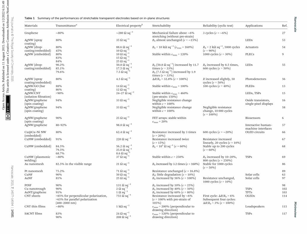
Considering the above limitations of out-of-planeapproaches, much effort has been dedicated to develop in-plane-structure-based stretchable transparent electrodes.Typical examples of in-plane structures include percolationnetworks of one-dimensional nanomaterials, such as metalnanowires and CNTs, as well as metal nanomeshes made ofultra-long metal nanofibers or nanotroughs. These entangledweb-like structures maintain their conductive pathways evenunder mechanical deformation owing to the structural reconfi-guration through sliding or rotating of nanomaterials againsteach other. In the following sections, various approachestoward the realization of in-plane-structure-based stretchabletransparent electrodes are described. The overall performancesof stretchable transparent electrodes based on in-plane struc-tures are summarized in Table 1.
3. Metal nanowires
Stretchable transparent electrodes based on in-plane configur-ations employing one-dimensional (1D) nanomaterials haveattracted much interest with an aim to overcome the above-mentioned drawbacks of out-of-plane structure-based stretch-able electrodes. 1D nanomaterials with high aspect ratios,such as CNTs and metal nanowires, can organize entangledpercolating networks using diverse techniques, including spincoating, spray coating, and drop casting.16,36–39 Among various1D nanomaterials, metal nanowires have been studied exten-sively due to their high electrical conductivity and mechanicalductility.
3.1. Ag nanowires
Ag is the most widely explored metal in its nanowire formowing to its highest electrical conductivity among variousmetals.36 Therefore, much effort has been dedicated to depositAg nanowires (AgNWs) on various substrates. AgNWs can besynthesized using various methods, such as the hydrothermalmethod, polyol process, microwave-assisted process, electro-chemical technique, UV irradiation technique, and template-assisted technique.40 Prior to the emerging interest in stretch-able electronics, AgNW was investigated as a promisingmaterial for flexible and transparent electrodes. Early flexibletransparent electrodes exploiting AgNWs were fabricated usingseveral techniques, such as vacuum filtration or Meyer rodcoating.41,42 These AgNW films were revealed to be thermally/chemically stable, as they maintained good conductivity evenafter the exposure to heat, water, and organic solvents (e.g.,acetone and isopropyl alcohol).42 However, as-prepared AgNWnetworks on substrates are not favourable in terms of thesurface roughness, and hence many studies have reportedseveral methods to improve the roughness, such as the coatingof PEDOT:PSS over the percolation network and the embed-ding of AgNWs into substrates.43–45 These AgNW electrodeswith improved roughness were used to demonstrate flexiblesolar cells and light-emitting diodes (LEDs).43–45 Much efforthas also been made to enhance the electrical performances of
AgNW films by reducing junction resistance or increasing per-colation paths. This has been achieved by employing variouswelding techniques or by introducing additional materialsinto the percolation networks.46–52
During the improvement of properties and fabricationsteps, stretchable transparent electrodes based on AgNWs havebeen studied at the same time to demonstrate stretchabledevices.9,53–56 Akter et al. provided a stretchable AgNW elec-trode by improving adhesion between a polymer substrate andAgNW networks using poly-dopamine.53 Spray-depositedAgNW electrodes showed excellent properties with a low sheetresistance of 35 Ω sq−1, high transmittance of about 80%, andan unchanged sheet resistance of up to 15% elongation.However, AgNW films that are directly coated on the substratehave undesirable high surface roughness. Alternatively, Pei’sgroup contrived the embedding method where AgNWs areembedded in various polymer substrates, such as poly(tert-butylacrylate-co-acrylic acid), poly(urethane acrylate), andethoxylated bisphenol A dimethacrylate with aromatic monoa-crylate.9,54,55 Adding acrylic acid (AA) into the polymer couldimprove the interactions between the polymer composite andAgNW networks. Fig. 2a and b show the effective transfer ofthe AgNWs into the polymer composite using AA. These fabri-cated transparent and stretchable electrodes were capable ofbeing used for actuators and polymer light-emitting electro-chemical cells (PLECs), as shown in Fig. 2c. More recently,Wang et al. reported a surfactant-assisted method using Zonylfluorosurfactant to reduce the process temperature.56 Theydemonstrated that the AgNW/PDMS polymer composite with asheet resistance of 4.5 Ω sq−1 and a transmittance of 80%could stretch up to 100% with resistance increased by 32.8%.
The single material of AgNW has clear limitations, such ashigh inter-nanowire junction resistances, dependence of sheetresistance on pattern sizes, chemical oxidation, and failuredue to electrical breakdown. Therefore, the formation ofhybrid structures with graphene oxide (GO), CNT, and gra-phene has been investigated to complement the limit-ations.6,13,15,16,57,58 As shown in Fig. 2d, the GO–AgNWnetwork fabricated by soaking the AgNW film into the GO dis-persion was introduced by Pei’s group to reduce the junctionresistance without any heat treatment.13 Here, GO flakes pro-vided a soldering effect between crossed AgNWs. This micro-structure of the GO–AgNW was applied to a LED with 14 Ωsq−1 sheet resistance and 88% transmittance at 550 nm. TheLED still operated even after 100 stretching cycles of 40%strain. More recently, hierarchical multiscale hybrid AgNW/CNT nanocomposites were introduced to achieve a high levelof mechanical compliance, conductivity, and transparency,simultaneously.15 In this hierarchical nanocomposite, CNTswrap the AgNW junctions and prevent the separation of junc-tions even at harsh stretching conditions. Although this workused the pre-strain method (εpre = 150%), the composite elec-trode retained its functionality even under a strain of 400%.The schematic and scanning electron microscopy (SEM)images of nanocomposites based on longer (thicker) AgNWs(diameter: ∼150 nm, length: ∼50–100 μm) and shorter
(thinner) CNTs (diameter: ∼1.2 nm, length: ∼2–10 μm) are pre-sented in Fig. 2e.
The combination of two-dimensional (2D) nanomaterials,such as graphene with AgNWs has been intensively explored aswell. Park’s group fabricated stretchable transparent electrodesbased on graphene and AgNWs, as shown in Fig. 2f.6,16,58
These hybrid structures achieved high transmittance (94%)and low resistance (33 Ω sq−1), which can be attributed to theincreased conducting pathways compared to the electrode con-sisting solely of AgNWs. Fig. 2g shows that the AgNW/graphenehybrid electrode can be stretched up to 100% with a negligiblechange in resistance. This hybrid electrode has been appliedto various stretchable and transparent electronics, includingLEDs (Fig. 2h), biosensors, and human–machine interfaces.6,16,57
3.2. Cu nanowires
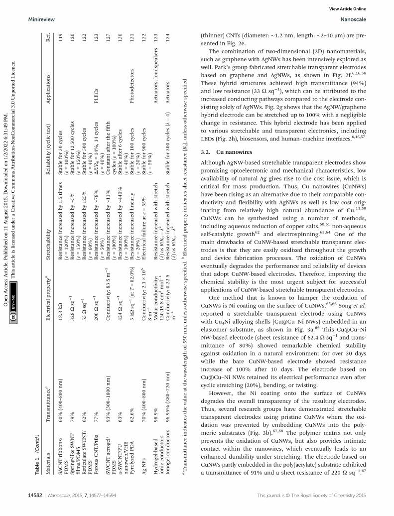
Although AgNW-based stretchable transparent electrodes showpromising optoelectronic and mechanical characteristics, lowavailability of natural Ag gives rise to the cost issue, which iscritical for mass production. Thus, Cu nanowires (CuNWs)have been rising as an alternative due to their comparable con-ductivity and flexibility with AgNWs as well as low cost orig-inating from relatively high natural abundance of Cu.11,59
CuNWs can be synthesized using a number of methods,including aqueous reduction of copper salts,60,61 non-aqueousself-catalytic growth62 and electrospinning.63,64 One of themain drawbacks of CuNW-based stretchable transparent elec-trodes is that they are easily oxidized throughout the growthand device fabrication processes. The oxidation of CuNWseventually degrades the performance and reliability of devicesthat adopt CuNW-based electrodes. Therefore, improving thechemical stability is the most urgent subject for successfulapplications of CuNW-based stretchable transparent electrodes.
One method that is known to hamper the oxidation ofCuNWs is Ni coating on the surface of CuNWs.65,66 Song et al.reported a stretchable transparent electrode using CuNWswith Cu4Ni alloying shells (Cu@Cu–Ni NWs) embedded in anelastomer substrate, as shown in Fig. 3a.66 This Cu@Cu–NiNW-based electrode (sheet resistance of 62.4 Ω sq−1 and trans-mittance of 80%) showed remarkable chemical stabilityagainst oxidation in a natural environment for over 30 dayswhile the bare CuNW-based electrode showed resistanceincrease of 100% after 10 days. The electrode based onCu@Cu–Ni NWs retained its electrical performance even aftercyclic stretching (20%), bending, or twisting.
However, the Ni coating onto the surface of CuNWsdegrades the overall transparency of the resulting electrodes.Thus, several research groups have demonstrated stretchabletransparent electrodes using pristine CuNWs where the oxi-dation was prevented by embedding CuNWs into the poly-meric substrates (Fig. 3b).67,68 The polymer matrix not onlyprevents the oxidation of CuNWs, but also provides intimatecontact within the nanowires, which eventually leads to anenhanced durability under stretching. The electrode based onCuNWs partly embedded in the poly(acrylate) substrate exhibiteda transmittance of 91% and a sheet resistance of 220 Ω sq−1.67T
The resistance increased by about 100% at the rupture strainof ∼15% (Fig. 3c) and showed a linearly increasing tendencyfor 20 stretching cycles of 15% elongation (Fig. 3d). Pei’sgroup added an additional chemical (6-aminohexanoic acid)to the polymer matrix to prevent the delamination of CuNWsfrom the polymeric substrate during the stretching.68 Theelectrode using 6-aminohexanoic acid showed less change inthe electrical performance compared to the electrode without6-aminohexanoic acid at 40% stretching, as shown in Fig. 3eand f.
The conventional thermal annealing process for thewelding of the junctions between nanowires also induces the
oxidation of CuNWs. To solve this problem, Han et al. reportedplasmonic nanowelding of CuNWs (Fig. 3g), which not onlyimproves the sheet resistance of resulting transparent electro-des, but also reduces the oxidation of CuNWs during thewelding process.69 The resulting electrode using plasmonic-nanowelded CuNWs exhibited a transmittance of ∼80% at550 nm and a sheet resistance of 37 Ω sq−1. The electrodetransferred onto an Eco-flex film endured a very large strain(>250%) with negligible resistance changes, and it was success-fully utilized for a touch screen panel, as shown in Fig. 3h.
According to some previous reports,69–73 welded metalnanowire (AgNW or CuNW) networks also show more stable
Fig. 2 AgNW-based stretchable transparent electrodes. (a) Cross-sectional SEM image of the conductive surface of a AgNW–poly(TBA-co-AA)composite. Scale bar, 1 μm. Reproduced with permission from ref. 54. Copyright 2012, John Wiley and Sons. (b) SEM image of the conductivesurface of the AgNW–polymer composite electrodes. Scale bar, 1 μm. Reproduced with permission from ref. 55. Copyright 2012, IOP Publishing. (c)Photographs of PLECs stretched at specified strains and wrapped around the edge of 400 mm-thick cardboard. Reproduced with permission fromref. 9. Copyright 2013, Nature Publishing Group. (d) SEM image of GO-soldered AgNW junctions (indicated by red arrows). Scale bar, 500 nm. Repro-duced with permission from ref. 13. Copyright 2014, American Chemical Society. (e) Schematic diagram (left) and SEM image (right) of the hierarchi-cal multiscale AgNW/CNT hybrid nanocomposite for highly stretchable conductors or highly transparent/flexible conductors. Scale bar, 300 nm.Reproduced with permission from ref. 15. Copyright 2014, John Wiley and Sons. (f ) Photograph of the graphene–AgNW hybrid film on a PET sub-strate. Scale bar, 2 cm. The inset shows a SEM image of this hybrid film (scale bar, 5 μm). Reproduced with permission from ref. 16. Copyright 2013,American Chemical Society. (g) The relative difference in the resistance of graphene–AgNW hybrid films on PDMS as a function of tensile straintoward uniaxial direction. Reproduced with permission from ref. 58. Copyright 2015, Springer. (h) Photograph of the ILED/graphene–AgNW hybridelectrode/contact lens device on an eye of a mannequin. (Inset: a photograph for emitting light of the contact lens device on a mannequin eye.Scale bar, 5 mm.) Reproduced with permission from ref. 16. Copyright 2013, American Chemical Society.
electrical performance under mechanical deformations thannon-welded networks. This can be ascribed to the differencein deformation between non-welded and welded networks.While a non-welded network accommodates strains by rotat-ing and/or sliding of each nanowire against others at the junc-tions, a welded network accommodates strains byreconfiguring the network structure in the same manner thata fishnet changes its shape when it is stretched. Thus, thejunctions in a non-welded network can be easily detached orbroken by bending or stretching, whereas the junctions in awelded network firmly connect distinct nanowires even underharsh stretching.
4. Metal nanomeshes
To achieve high quality stretchable transparent electrodesusing metal nanowires, defect-free nanowires should be syn-thesized with conductivities close to those of bulkmetals.38,41,52,63,74–76 These refined metal nanowires shouldthen be carefully deposited on a substrate with a density abovethe percolation threshold to provide sufficient current pathswithin the percolation networks.77,78 This percolationthreshold could be fulfilled more easily if metal nanowires hadhigher aspect ratios.77 Additionally, ultra-long metal nanowiresreduce the dependence of total resistance of transparent
Fig. 3 CuNW-based stretchable transparent electrodes. (a) Schematic illustration of Cu@Cu–Ni NWs embedded in an elastomer substrate. Repro-duced with permission from ref. 66. Copyright 2014, American Chemical Society. (b) Schematic illustration of the fabrication process of a CuNW–PUcomposite electrode. Reproduced with permission from ref. 68. Copyright 2013, Royal Society of Chemistry. (c) Resistance change of a CuNW/poly-(acrylate) electrode (R0 = 5.8 Ω) during the first stretching and releasing. (d) Resistance change for a 5 Ω CuNW/poly(acrylate) electrode being cycledbetween 0% and 10% strain for 20 times. (c and d) Reproduced with permission from ref. 67. Copyright 2014, Royal Society of Chemistry. (e and f)Normalized transient resistance of (e) pristine CuNW/PU composite electrodes and (f ) 6-aminohexanoic acid pretreated CuNW/PU composite elec-trodes during the cyclic stretching–releasing process with the peak strain of 40% at the stretching speed of 0.01 mm s−1. (e and f) Reproduced withpermission from ref. 68. Copyright 2013, Royal Society of Chemistry. (g) Schematic illustration of the plasmonic laser nanowelding process ofCuNWs. (h) Demonstration of the touch-screen panel fabricated with a laser-nanowelded CuNW transparent conductor. (g and h) Reproduced withpermission from ref. 69. Copyright 2014, John Wiley and Sons.
electrodes on the junction resistances between nanowires.Based on this idea, alternative nanostructures, such as nano-meshes, nanofibers, and nanotroughs, have been extensivelyexplored to realize stretchable transparent electrodes.
4.1. Metal grids
A metal grid with a grating structure is the most basic form ofa metal nanomesh for flexible or stretchable transparent elec-trodes. The transmittance and sheet resistance of metal gridscan be controlled using key parameters such as film thickness,grid line width and grid pattern pitch.79,80 To obtain hightransmittance (above 90% at 550 nm) and maintain low sheetresistance, the grid line width should be reduced and the gridpattern pitch should be optimized considering the trade-offbetween sheet resistance and transmittance. In addition to theconventional photolithography,80–82 which requires multiplefabrication steps, including a vacuum process, various fabrica-tion methods have been utilized to demonstrate metal gridelectrodes, including inkjet printing,83 electrohydrodynamicinkjet,79,84 direct writing,85 and imprinting.74
Although the optoelectronic characteristics of metal gridelectrodes can be readily tuned, they only present the stretch-ability along a diagonal direction to the grating pattern. Theelongation of the grating pattern along the orthogonal direc-tions is likely to induce undesired cracks or failure of the elec-trode. Therefore, metal grids with random or meanderingnetworks have recently been investigated to obtain the stretch-ability without any directivity. Guo et al. reported a stretchabletransparent Au nanomesh electrode using grain boundarylithography.86 This electrode showed a sheet resistance of 21 Ωsq−1 and a transmittance of 82.5%. Also, it can be stretched upto 160% with the sheet resistance increased by 3.2 times. Theyalso reported the recovery effect of Au nanomesh electrodesunder cyclic stretching or compression by taking advantage ofthe cold-welding phenomenon, where welding of damagedparts occurs due to the pressures induced by mechanicaldeformation,87 thereby providing a durable and generallyapplicable stretchable transparent electrode.88 Jang et al.reported a hexagonal Pt nanomesh electrode using anodizedaluminium oxide (AAO) template as a substrate. Pt was sput-tered on an AAO template and then the AAO template wasremoved, providing a transferable Pt nanomesh with a honey-comb structure.89 This Pt nanomesh electrode showed a sheetresistance of 71 Ω sq−1 with a transmittance of 75.2%, and itcould be stretched up to 16.8% without any significantchanges in resistance.
4.2. Metal nanofibers and nanotroughs
As mentioned previously, the meandering design90 andsmaller line width79,80 are prerequisites for preferable stretch-able transparent electrodes. Therefore, conducting randomnetworks with high aspect ratio nanomaterials beyond nano-wires are required.91 Based on this idea, metallic nanofibershave been attracting substantial interest as an alternativematerial for stretchable transparent electrodes. Most metallicnanofibers have been fabricated by electrospinning, which is a
facile method to make continuous and long nanofibers frompolymeric solutions using electrohydrodynamics.92,93
The first attempt to fabricate metallic nanofibers via elec-trospinning adopted the precursor-based method,63,94–96
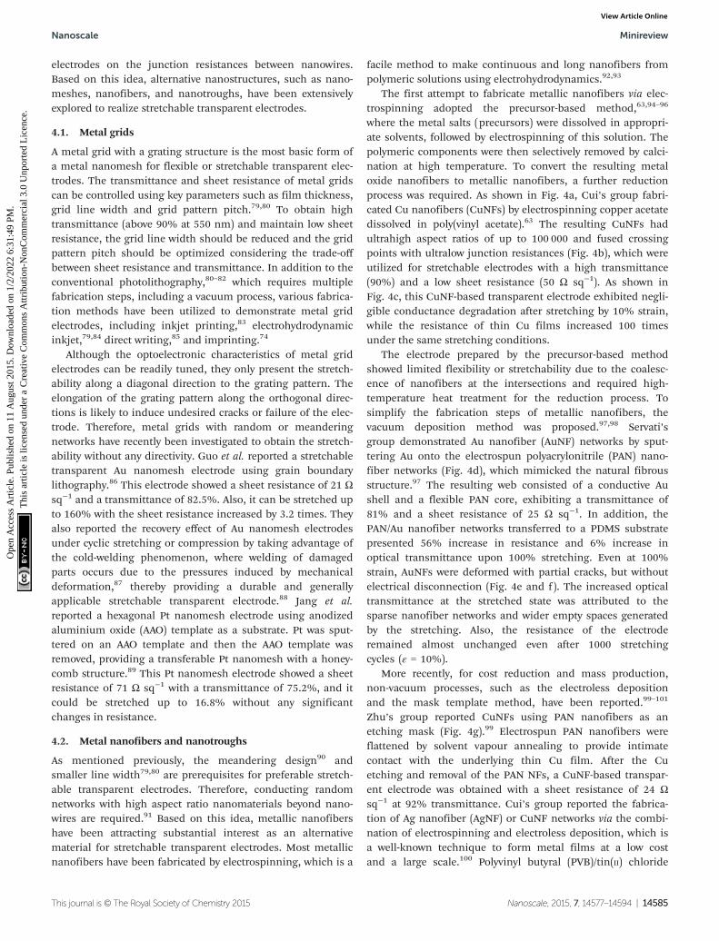
where the metal salts (precursors) were dissolved in appropri-ate solvents, followed by electrospinning of this solution. Thepolymeric components were then selectively removed by calci-nation at high temperature. To convert the resulting metaloxide nanofibers to metallic nanofibers, a further reductionprocess was required. As shown in Fig. 4a, Cui’s group fabri-cated Cu nanofibers (CuNFs) by electrospinning copper acetatedissolved in poly(vinyl acetate).63 The resulting CuNFs hadultrahigh aspect ratios of up to 100 000 and fused crossingpoints with ultralow junction resistances (Fig. 4b), which wereutilized for stretchable electrodes with a high transmittance(90%) and a low sheet resistance (50 Ω sq−1). As shown inFig. 4c, this CuNF-based transparent electrode exhibited negli-gible conductance degradation after stretching by 10% strain,while the resistance of thin Cu films increased 100 timesunder the same stretching conditions.
The electrode prepared by the precursor-based methodshowed limited flexibility or stretchability due to the coalesc-ence of nanofibers at the intersections and required high-temperature heat treatment for the reduction process. Tosimplify the fabrication steps of metallic nanofibers, thevacuum deposition method was proposed.97,98 Servati’sgroup demonstrated Au nanofiber (AuNF) networks by sput-tering Au onto the electrospun polyacrylonitrile (PAN) nano-fiber networks (Fig. 4d), which mimicked the natural fibrousstructure.97 The resulting web consisted of a conductive Aushell and a flexible PAN core, exhibiting a transmittance of81% and a sheet resistance of 25 Ω sq−1. In addition, thePAN/Au nanofiber networks transferred to a PDMS substratepresented 56% increase in resistance and 6% increase inoptical transmittance upon 100% stretching. Even at 100%strain, AuNFs were deformed with partial cracks, but withoutelectrical disconnection (Fig. 4e and f). The increased opticaltransmittance at the stretched state was attributed to thesparse nanofiber networks and wider empty spaces generatedby the stretching. Also, the resistance of the electroderemained almost unchanged even after 1000 stretchingcycles (ε = 10%).
More recently, for cost reduction and mass production,non-vacuum processes, such as the electroless depositionand the mask template method, have been reported.99–101
Zhu’s group reported CuNFs using PAN nanofibers as anetching mask (Fig. 4g).99 Electrospun PAN nanofibers wereflattened by solvent vapour annealing to provide intimatecontact with the underlying thin Cu film. After the Cuetching and removal of the PAN NFs, a CuNF-based transpar-ent electrode was obtained with a sheet resistance of 24 Ωsq−1 at 92% transmittance. Cui’s group reported the fabrica-tion of Ag nanofiber (AgNF) or CuNF networks via the combi-nation of electrospinning and electroless deposition, which isa well-known technique to form metal films at a low costand a large scale.100 Polyvinyl butyral (PVB)/tin(II) chloride
(SnCl2) NFs were first formed by electrospinning, and thenimmersed in the silver nitrate (AgNO3) aqueous solution toform the Ag seed layer only on the surface of nanofibers.Subsequent metallization via electroless deposition providedAgNF or CuNF networks, achieving a sheet resistance ofaround 10 Ω sq−1 and a transmittance of 90% (Fig. 4h).These electrodes, however, still exhibited limited flexibilityand stretchability due to the coalescence of nanofiberjunctions.
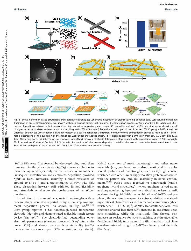
In addition to the nanofibers, metal nanotroughs with aconcave shape were also reported using a low step coveragemetal deposition process, as shown in Fig. 5a.102–104
Cui’s group reported a Cu nanotrough-based transparentelectrode (Fig. 5b) and demonstrated a flexible touch-screendevice (Fig. 5c).102 The electrode had outstanding opto-electronic performance (sheet resistance: ∼2 Ω sq−1, transmit-tance: 90%) and showed reasonable stretchability (∼40%increase in resistance upon 50% uniaxial tensile strain).
Hybrid structures of metal nanotroughs and other nano-materials (e.g., graphene) were also investigated to resolveseveral problems of nanotroughs, such as (i) high contactresistance with other layers, (ii) percolation problem associatedwith the pattern size, and (iii) instability in harsh environ-ments.99,103 Park’s group reported Au nanotrough (AuNT)/graphene hybrid structures,103 where graphene served as anauxiliary conducting layer and an anti-oxidation layer as well,as shown in Fig. 5d. With the combination of AuNTs and gra-phene, the resulting transparent electrode exhibited outstand-ing electrical characteristics with remarkable uniformity (sheetresistance: 1 ± 0.1 Ω sq−1) at 91% transmittance. Also, thiselectrode showed less than 60% increase in resistance upon80% stretching, while the AuNT-only film showed 60%increase in resistance for 50% stretching. A skin-attachable,flexible, and highly transparent thin film transistor backplanewas demonstrated using this AuNT/graphene hybrid electrode(Fig. 5e–g).
Fig. 4 Metal nanofiber-based stretchable transparent electrodes. (a) Schematic illustration of electrospinning of nanofibers. Left column: schematicillustration of an electrospinning setup, shown without a syringe pump. Right column: the fabrication process of Cu nanofibers. (b) Schematic illus-tration of junctions between solution-processed Ag nanowires (upper) and electrospun Cu nanofibers (down). (c) Cu nanofiber networks with smallchanges in terms of sheet resistance upon stretching with 10% strain. (a–c) Reproduced with permission from ref. 63. Copyright 2010, AmericanChemical Society. (d) Cross sectional SEM micrograph of a sparse nanofiber transparent conductor web embedded in an epoxy resin. (e and f) Sche-matic illustrations of the evolution of the nanofiber web under the applied strain. (d–f ) Reproduced with permission from ref. 97. Copyright 2013,John Wiley and Sons. (g) Scheme of Cu nanowire (nanofiber) network electrode fabrication. Reproduced with permission from ref. 99. Copyright2014, American Chemical Society. (h) Schematic illustration of electroless deposited metallic electrospun nanowire transparent electrodes.Reproduced with permission from ref. 100. Copyright 2014, American Chemical Society.
Apart from the above-mentioned methods, several distinctapproaches have been developed for stretchable transparentelectrodes, including CNTs, metal nanoparticle-incorporatedcomposites, and hydrogel-based ionic conductors. Theseunique approaches have diversified the application of stretch-able transparent electrodes.
5.1. Carbon nanotubes
CNT is one of the most famous allotropes of carbon with ahigh aspect ratio cylindrical tube shape composed of one ormore layers of graphitic carbon (single-walled CNT (SWCNT)or multi-walled CNT).105,106 These cylindrical structures ofcarbon have remarkable properties, such as high mechanicalstrength, thermal conductivity, and electrical conductivity.107–109
CNTs can be synthesized using various simple methods, whilechemical vapour deposition (CVD), arc discharge, and laser
ablation are the most commonly used methods.110–112 Sincethe initial discovery of the CNT in 1991,105 tremendousnumber of studies have been conducted on CNTs, owing to itsunique properties and relatively simple preparation methods.
The early studies on stretchable conductors or electrodesbased on CNTs focused on the CNT/polymer composite. CNTswith outstanding mechanical and electrical properties wereattractive filler materials blended with a polymer matrix.113
Although CNT/polymer composites were suitable for stretch-able conductors, most of them were not optically transparentdue to the high concentration of CNT fillers. To expand theusage of stretchable CNT electrodes, many interesting studieshave been carried out to improve the optical transparency ofCNT-based electrodes.
5.1.1. Aligned CNTs. The initial strategy to render CNT-based stretchable transparent electrodes was to use directlydrawn aligned CNTs from a CNT forest, as shown in Fig. 6a.114
These unidirectional, transparent and stretchable CNT sheets
Fig. 5 Metal nanotrough-based stretchable transparent electrodes. (a) SEM image of the cross-section of a single Au nanotrough, revealing itsconcave shape. (b) Schematic illustration of the polymer–nanofiber templating process for fabricating nanotroughs. (c) Photograph of metal nano-trough on a PET film as a transparent electrode for touch screen. (a–c) Reproduced with permission from ref. 102. Copyright 2013, Nature PublishingGroup. (d) Schematic images of the processes to form the graphene–metal nanotrough hybrid electrode. (e) A photo (left) of the TFT array samplemade by graphene–metal nanotrough hybrid electrodes on a transparent polyimide substrate. Scale bar, 1 cm. A schematic diagram (right) ofthe TFT layout. (f ) Statistical distributions of mobility characteristics of the transistor made by graphene–metal nanotrough hybrid electrodes inlinear or saturation regimes. (g) Photographs of the TFT arrays transferred on a leaf, eyeglasses, and the skin of human hand. All scale bars, 1 cm.(d–g) Reproduced with permission from ref. 103. Copyright 2014, American Chemical Society.
with a meter-long scale (up to several centimetres wide) wereutilized as electrodes for organic light-emitting diodes(OLEDs) (Fig. 6b),114 loudspeakers,115 supercapacitors,116 andtouch panels (Fig. 6c).117 However, these CNT sheets were an-isotropic with regard to optical, electrical, and mechanical pro-perties due to the fixed drawing direction (e.g., transmittanceof a CNT sheet was >85% for perpendicular polarization and>65% for parallel polarization).114 These anisotropic character-
istics of highly aligned CNT sheets were the main obstacles tobe utilized as stretchable transparent electrodes. In thisregard, several studies have been conducted to improve theirlimited characteristics.
Based on a previous report,115 where CNT sheets drawnfrom a short height of the CNT forest had no large bundlesand achieved high transmittance, Feng et al.117 reportedhighly transparent and roll-to-roll processable superaligned
Fig. 6 CNT-based stretchable transparent electrodes. (a) Photograph of a self-supporting 3.4 cm-wide, meter-long MWNT sheet that has beenhand drawn from a nanotube forest at an average rate of 1 m min−1. (b) Photograph of an OLED that uses a solid-state-fabricated aligned MWNTsheet as the hole-injecting electrode. (a and b) Reproduced with permission from ref. 114. Copyright 2005, The American Association for theAdvancement of Science. (c) Transparent and flexible touch panels based on SACNT films. Reproduced with permission from ref. 117. Copyright2010, John Wiley and Sons. (d) Sheet resistance of 4-layer cross-stacked films along the three specific directions indicated in the inset illustration.Reproduced with permission from ref. 118. Copyright 2011, John Wiley and Sons. (e) Evolution of morphology of CNT films with stretching. Sche-matics (top) and corresponding AFM phase images (bottom) of CNT films. All scale bars, 600 nm. Reproduced with permission from ref. 120. Copy-right 2011, Nature Publishing Group. (f ) SEM image of the as-grown SWCNT films. Scale bar, 500 nm. The insets show the comparison of thehierarchical reticulate structures of the SWCNT film (left) and the leaf veins (right). Reproduced with permission from ref. 122. Copyright 2012, JohnWiley and Sons. (g) Fabrication process of the SWCNT/PU nanoweb to produce a transparent, elastic conductor. Reproduced with permission fromref. 130. Copyright 2012, Royal Society of Chemistry.
CNT (SACNT) films by reducing the height of the CNT forestand removing residual large bundles in SACNT films withplasma and laser trimming, respectively. Oxygen plasmaeffectively reduced the height of a SACNT array, and lasertrimming removed the outermost CNTs of large bundlesfrom as-drawn SACNT films. In addition, to achieve betterelectrical conductivity, metals (Au or Ag) were deposited ontothe SACNT film, which then exhibited excellent opto-electronic performances with sheet resistances and transmit-tances of 208 Ω sq−1 at 90% or 24 Ω sq−1 at 83.4%,respectively. The same research group then reported a cross-stacked structure of SACNT films to solve the anisotropy, asshown in Fig. 6d. The resulting SACNT film could bestretched up to 35% along a diagonal direction relative to thestacking angle.118
Despite the above-mentioned interesting progress in thealigned CNT approach, the transparent electrodes made ofaligned CNTs showed incomplete stretchability in that theyundergo irreversible plastic deformation upon a tensilestrain.118 Several strategies to solve this problem were demon-strated by embedding aligned CNTs into the elastomericmatrix.118,119 The resulting electrode exhibited nearlyunchanged resistance (35.5 ± 0.3 kΩ) after 6 cycles of 100%stretching.119
5.1.2. Random network CNTs. In addition to the alignedCNTs, random networks of CNTs have also been introducedfor stretchable transparent electrodes via direct depositiononto or embedding into elastomers. Lipomi et al.120 obtainedspring-like buckled 2D SWCNT films (Fig. 6e) by stretchingand releasing the as-sprayed random network CNTs on aPDMS substrate. This electrode had a sheet resistance of 328 Ωsq−1 with a transmittance of 79% and survived even at 150%tensile strain. Free-standing SWCNT films with hierarchicalreticulate structures were directly synthesized by a floating-catalyst CVD, which provided stretchable transparent electro-des.121 To impart further stretchability, Cai et al.122 embeddedthe SWCNT film with a hierarchical reticulate structure into aPDMS substrate (Fig. 6f), providing a stretchable transparentelectrode with a transmittance of 62% at 550 nm and a sheetresistance of 53 Ω sq−1, which exhibited 125% increase upon atensile strain of 60%.
Another approach was also demonstrated with a compositeof a porous SWCNT three-dimensional (3D) network and elas-tomer. Yu et al.123 reported the fabrication of nanoporousSWCNT network–polymer composites by Meyer rod coating124
and in situ UV curing of tert-butyl acrylate. This electrodeshowed a transmittance of >77% and a sheet resistance of200 Ω sq−1, which increased by 78% under a 50% tensile strain.It was utilized as both the anode and cathode for PLECs.Another interesting method to fabricate porous SWCNT 3Dnetworks was also reported, where ultralight and electricallyconducting SWCNT aerogels were prepared by the freeze-drying method.125,126 SWCNT aerogel-based PDMS compositeswere obtained through the penetration of PDMS into theporous SWCNT aerogel.127 This highly stretchable and trans-parent (maximum ε = 250% and T = 90%) electrodes showed
no significant changes in resistance after 20 cycles of 100%stretching.
Electrospun nanofiber-assisted SWCNT–polymer nanowebhas been emerging as another strategy to obtain randomSWCNT network-based electrodes. CNTs can effectively formwell-connected conducting networks without agglomeration bysimple drop-casting on a well-distributed polymer nanofiberscaffold.128,129 Kim et al.130 also created an acid-treatedSWCNT network on web-shaped polyurethane nanofibersthrough simple electrospinning and dip-coating methods, asshown in Fig. 6g. Utilizing the stretching–releasing method,stretchable electrodes with noodle-like structures wereachieved, which exhibited a sheet resistance of 424 Ω sq−1 at63% transmittance and sustained stable conductivity after6 cycles of 100% stretching.
5.2. Other approaches for stretchable transparent electrodes
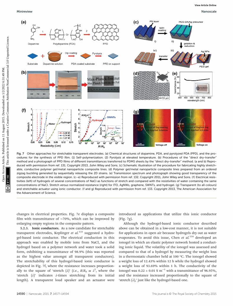
Besides metal nanomaterials and CNTs, several unconven-tional strategies have been developed to realize stretchabletransparent electrodes, such as bio-inspired fabrication ofstretchable carbon films,131 polymer gel/metal nanoparticlecomposites,132 and hydrogel-based ionic conductors.133,134
5.2.1. Pyrolyzed polydopamine. A carbon-based stretch-able transparent electrode was demonstrated on a PDMS sub-strate using pyrolyzed polydopamine (PDA) films.131 Thepyrolyzed PDA film was prepared by immersion of a substratein a self-polymerizable dopamine solution and subsequentpyrolysis at high temperature (800–1000 °C), as shown inFig. 7a. The pyrolyzed PDA film prepared in this low-cost andscalable process may be regarded as a multi-layered graphenefilm. As shown in Fig. 7b, the pyrolyzed PDA film on a Cu foilwas dry-transferred to a PDMS substrate, resulting in a stretch-able transparent electrode (T = 62.6%). The resistanceincreased linearly (R/R0 ≅ 50) upon stretching from 0% to20%. A cyclic stretching test (ε = 20%) showed reliability of theelectrode without significant changes in electrical properties.A photodetector with rapid and repeatable sensing was demon-strated as well using this pyrolyzed PDA electrode.
5.2.2. Polymer gel/metal nanoparticle composites. A metalnanoparticle-based composite was reported by Hyun et al.132
as a promising candidate for stretchable transparent electro-des. A mixture of a UV-crosslinkable polymer (poly(ethyleneoxide)-diacrylate (PEG-DA)) and a metal precursor (silver tri-fluoroacetate (STA)) was spin-coated on the polystyrene (PS)-coated PDMS substrate with a wavy structure, as shown inFig. 7c. Subsequent UV exposure and chemical reductionyielded PEG gel/Ag nanoparticle composite patterns, whichwere then transferred to a new elastomer substrate with a flat-tening of the wavy PDMS template by applying a tensile strain.The stretchability was achieved by 2D zigzag patterns of thecomposite generated by releasing of the wavy template(Fig. 7d). This composite pattern exhibited conductivity of∼106 S m−1 at 50% strain without electrical degradation;however, it showed dramatic decrease in conductivity at 55%strain due to mechanical failure. Repeated stretching (900cycles for 20% strain) of this electrode caused no substantial
changes in electrical properties. Fig. 7e displays a compositefilm with transmittance of ∼70%, which can be improved byenlarging empty regions in the composite pattern.
5.2.3. Ionic conductors. As a new candidate for stretchabletransparent electrodes, Keplinger et al.133 suggested a hydro-gel-based ionic conductor. The electrical conduction in thisapproach was enabled by mobile ions from NaCl, and thehydrogel based on a polymer network and water took a solidform, exhibiting a transmittance of 98.9% (this was reportedas the highest value amongst all transparent conductors).The stretchability of this hydrogel-based ionic conductor isdepicted in Fig. 7f, where the resistance increases proportion-ally to the square of ‘stretch (λ)’ (i.e., R/R0 ∝ λ2, where the‘stretch (λ)’ indicates λ-times stretching from its initiallength). A transparent loud speaker and an actuator were
introduced as applications that utilize this ionic conductor(Fig. 7g).
Although the hydrogel-based ionic conductor describedabove can be obtained in a low-cost manner, it is not suitablefor applications in open air because hydrogels dry out as waterevaporates. To avoid this issue, Chen et al.134 developed anionogel in which an elastic polymer network hosted a conduct-ing ionic liquid. The volatility of the ionogel was assessed andcompared to that of a hydrogel by measuring the weight lossin a thermostatic chamber held at 100 °C. The ionogel showeda weight loss of 12.43% within 12 h while the hydrogel showeda weight loss of 93.69% within 1 h. The conductivity of theionogel was 0.22 ± 0.01 S m−1 with a transmittance of 96.95%,and the resistance increased proportionally to the square of‘stretch (λ),’ just like the hydrogel-based one.
Fig. 7 Other approaches for stretchable transparent electrodes. (a) Chemical structures of dopamine, PDA, and pyrolyzed PDA (PPD), and the pro-cedures for the synthesis of PPD film. (1) Self-polymerization. (2) Pyrolysis at elevated temperature. (b) Procedures of the “direct dry-transfer”method and a photograph of PPD films of different transmittances transferred to PDMS sheets by the “direct dry-transfer” method. (a and b) Repro-duced with permission from ref. 131. Copyright 2013, John Wiley and Sons. (c) Schematic illustration of the procedure for fabricating highly stretch-able, conductive polymer gel/metal nanoparticle composite lines. (d) Polymer gel/metal nanoparticle composite lines prepared from an orderedzigzag buckling generated by sequentially releasing the 2D strains. (e) Transmission spectrum and photograph showing good transparency of thecomposite electrode in the visible region. (c–e) Reproduced with permission from ref. 132. Copyright 2011, John Wiley and Sons. (f ) Electrical resis-tivities (left) of hydrogels of several concentrations of NaCl as functions of stretch and compared with the resistivities of water containing the sameconcentrations of NaCl. Stretch versus normalized resistance (right) for ITO, AgNWs, graphene, SWNTs, and hydrogel. (g) Transparent (to all colours)and stretchable actuator using ionic conductor. (f and g) Reproduced with permission from ref. 133. Copyright 2013, The American Association forthe Advancement of Science.
We have witnessed surprising advances in stretchable elec-tronics over the past decade. As an essential component forstretchable electronics, stretchable transparent thin-film elec-trodes have progressed remarkably, as summarized in thismini review. Metal nanomaterials, such as nanowires, nano-fibers, and nanotroughs, exhibit promising characteristicseven under high-level mechanical deformation. Also, CNTsand other unique approaches increase the number of feasibleoptions for stretchable transparent electrodes.
Stretchable transparent electrodes based on in-plane con-figurations, however, still require further improvement inseveral aspects. First, the preparation of high-quality anddefect-free nanomaterials should be further refined for accep-table functionalities of electrodes thereof. The chemical stabi-lity (e.g., stability against oxidation) of these nanomaterialsalso needs to be enhanced to guarantee the reliable long-termoperation of resulting devices in practical uses. The hybridiz-ation of nanomaterials (e.g., AgNWs + graphene) has provenfeasible by combining the strengths and compensating theweaknesses of each material, and should be further investi-gated by exploiting various materials and hierarchical struc-tures. In addition to the material itself, adhesion andinterfacial interactions of stretchable transparent electrodeswith elastomeric substrates and other constituting active com-ponents should be considered as well for the durable oper-ation of final products. Lastly, scalable and low-temperaturefabrication processes depending on the materials should bedeveloped in a low-cost manner to facilitate the advent of prac-tical stretchable electronics.
We are now about to see a great leap of electronics towardsstretchable form where conventional constraints from rigidform-factors no longer matter. Tremendous research effortsover the past decade have revealed a cornucopia of stretchableelectronics with regard to research opportunities and potentialapplications. Unprecedented applications employing stretch-able electronics, including biomedical, healthcare, and wear-able devices, are expected to emerge and change our ways oflife in the near future.
Acknowledgements
This work was supported by the Ministry of Science, ICT &Future Planning and the Ministry of Trade, Industry andEnergy of Korea through Basic Science Research Program ofNational Research Foundation (2013R1A2A2A01068542),Materials Original Technology Program (10041222), Techno-logy Innovation Program (Grant 10044410), ConvergenceTechnology Development Program for Bionic Arm(NRF-2014M3C1B2048198), and Pioneer Research CenterProgram (NRF-2014M3C1A3001208). Also, the authors thankSamsung Display and financial support by the DevelopmentPrograms of Manufacturing Technology for Flexible Electronicswith High Performance (SC0970) funded by Korea Institute of
Machinery and Materials and by Development of InterconnectSystem and Process for Flexible Three Dimensional Hetero-geneous Devices funded by MOTIE in Korea.
Notes and references
1 J. A. Rogers, T. Someya and Y. Huang, Science, 2010, 327,1603–1607.
2 T. Sekitani and T. Someya, Adv. Mater., 2010, 22, 2228–2246.
3 D.-H. Kim and J. A. Rogers, Adv. Mater., 2008, 20, 4887–4892.
4 M. Kaltenbrunner, T. Sekitani, J. Reeder, T. Yokota,K. Kuribara, T. Tokuhara, M. Drack, R. Schwödiauer,I. Graz, S. Bauer-Gogonea, S. Bauer and T. Someya, Nature,2013, 499, 458–463.
5 J. Kim, M. Lee, H. J. Shim, R. Ghaffari, H. R. Cho, D. Son,Y. H. Jung, M. Soh, C. Choi, S. Jung, K. Chu, D. Jeon,S.-T. Lee, J. H. Kim, S. H. Choi, T. Hyeon and D.-H. Kim,Nat. Commun., 2014, 5, 5747.
6 J. Kim, M.-S. Lee, S. Jeon, M. Kim, S. Kim, K. Kim, F. Bien,S. Y. Hong and J.-U. Park, Adv. Mater., 2015, 27, 3292–3297.
7 J. Zang, S. Ryu, N. Pugno, Q. Wang, Q. Tu, M. J. Buehlerand X. Zhao, Nat. Mater., 2013, 12, 321–325.
8 M. S. White, M. Kaltenbrunner, E. D. Głowacki,K. Gutnichenko, G. Kettlgruber, I. Graz, S. Aazou,C. Ulbricht, D. A. M. Egbe, M. C. Miron, Z. Major,M. C. Scharber, T. Sekitani, T. Someya, S. Bauer andN. S. Sariciftci, Nat. Photonics, 2013, 7, 811–816.
9 J. Liang, L. Li, X. Niu, Z. Yu and Q. Pei, Nat. Photonics,2013, 7, 817–824.
10 S. Xu, Y. Zhang, J. Cho, J. Lee, X. Huang, L. Jia, J. A. Fan,Y. Su, J. Su, H. Zhang, H. Cheng, B. Lu, C. Yu, C. Chuang,T. Kim, T. Song, K. Shigeta, S. Kang, C. Dagdeviren,I. Petrov, P. V. Braun, Y. Huang, U. Paik and J. A. Rogers,Nat. Commun., 2013, 4, 1543.
11 S. Yao and Y. Zhu, Adv. Mater., 2015, 27, 1480–1511.12 T. Cheng, Y. Zhang, W.-Y. Lai and W. Huang, Adv. Mater.,
2015, 27, 3349–3376.13 J. Liang, L. Li, K. Tong, Z. Ren, W. Hu, X. Niu, Y. Chen
and Q. Pei, ACS Nano, 2014, 8, 1590–1600.14 D. J. Lipomi, B. C.-K. Tee, M. Vosgueritchian and Z. Bao,
Adv. Mater., 2011, 23, 1771–1775.15 P. Lee, J. Ham, J. Lee, S. Hong, S. Han, Y. D. Suh,
S. E. Lee, J. Yeo, S. S. Lee, D. Lee and S. H. Ko, Adv. Funct.Mater., 2014, 24, 5671–5678.
16 M.-S. Lee, K. Lee, S.-Y. Kim, H. Lee, J. Park, K.-H. Choi,H.-K. Kim, D.-G. Kim, D.-Y. Lee, S. Nam and J.-U. Park,Nano Lett., 2013, 13, 2814–2821.
17 M. Drack, I. Graz, T. Sekitani, T. Someya,M. Kaltenbrunner and S. Bauer, Adv. Mater., 2015, 27, 34–40.
18 D.-H. Kim, J. Xiao, J. Song, Y. Huang and J. A. Rogers, Adv.Mater., 2010, 22, 2108–2124.
19 W. M. Choi, J. Song, D.-Y. Khang, H. Jiang, Y. Y. Huangand J. A. Rogers, Nano Lett., 2007, 7, 1655–1663.
20 Y. Shang, X. He, Y. Li, L. Zhang, Z. Li, C. Ji, E. Shi, P. Li,K. Zhu, Q. Peng, C. Wang, X. Zhang, R. Wang, J. Wei,K. Wang, H. Zhu, D. Wu and A. Cao, Adv. Mater., 2012, 24,2896–2900.
21 F. Xu, W. Lu and Y. Zhu, ACS Nano, 2011, 5, 672–678.22 K. S. Novoselov, A. K. Geim, S. V. Morozov, D. Jiang,
Y. Zhang, S. V. Dubonos, I. V. Grigorieva and A. A. Firsov,Science, 2004, 306, 666–669.
23 A. K. Geim and K. S. Novoselov, Nat. Mater., 2007, 6, 183–191.
24 K. S. Novoselov, V. I. Fal′ko, L. Colombo, P. R. Gellert,M. G. Schwab and K. Kim, Nature, 2012, 490, 192–200.
25 F. Bonaccorso, Z. Sun, T. Hasan and A. C. Ferrari, Nat.Photonics, 2010, 4, 611–622.
26 S. Bae, H. Kim, Y. Lee, X. Xu, J.-S. Park, Y. Zheng,J. Balakrishnan, T. Lei, H. Ri Kim, Y. I. Song, Y.-J. Kim,K. S. Kim, B. Ozyilmaz, J.-H. Ahn, B. H. Hong andS. Iijima, Nat. Nanotechnol., 2010, 5, 574–578.
27 K. S. Kim, Y. Zhao, H. Jang, S. Y. Lee, J. M. Kim, K. S. Kim,J.-H. Ahn, P. Kim, J.-Y. Choi and B. H. Hong, Nature, 2009,457, 706–710.
28 T.-H. Han, Y. Lee, M.-R. Choi, S.-H. Woo, S.-H. Bae,B. H. Hong, J.-H. Ahn and T.-W. Lee, Nat. Photonics, 2012,6, 105–110.
29 J.-H. Ahn and B. H. Hong, Nat. Nanotechnol., 2014, 9, 737–738.
30 S.-K. Lee, H. Y. Jang, S. Jang, E. Choi, B. H. Hong, J. Lee,S. Park and J.-H. Ahn, Nano Lett., 2012, 12, 3472–3476.
31 T. Chen, Y. Xue, A. K. Roy and L. Dai, ACS Nano, 2014, 8,1039–1046.
32 J.-H. Ahn and J. H. Je, J. Phys. D: Appl. Phys., 2012, 45,103001.
33 M. Vosgueritchian, D. J. Lipomi and Z. Bao, Adv. Funct.Mater., 2012, 22, 421–428.
34 Y. G. Seol, T. Q. Trung, O.-J. Yoon, I.-Y. Sohn andN.-E. Lee, J. Mater. Chem., 2012, 22, 23759–23766.
35 M. Kaltenbrunner, M. S. White, E. D. Głowacki,T. Sekitani, T. Someya, N. S. Sariciftci and S. Bauer, Nat.Commun., 2012, 3, 770.
36 C. Yang, H. Gu, W. Lin, M. M. Yuen, C. P. Wong, M. Xiongand B. Gao, Adv. Mater., 2011, 23, 3052–3056.
37 A. R. Madaria, A. Kumar and C. Zhou, Nanotechnology,2011, 22, 245201.
38 V. Scardaci, R. Coull, P. E. Lyons, D. Rickard andJ. N. Coleman, Small, 2011, 7, 2621–2628.
39 J.-Y. Lee, S. T. Connor, Y. Cui and P. Peumans, Nano Lett.,2008, 8, 689–692.
40 D. Langley, G. Giusti, C. Mayousse, C. Celle, D. Bellet andJ.-P. Simonato, Nanotechnology, 2013, 24, 452001.
41 S. De, T. M. Higgins, P. E. Lyons, E. M. Doherty,P. N. Nirmalraj, W. J. Blau, J. J. Boland and J. N. Coleman,ACS Nano, 2009, 3, 1767–1774.
42 L. Hu, H. S. Kim, J.-Y. Lee, P. Peumans and Y. Cui, ACSNano, 2010, 4, 2955–2963.
43 L. Yang, T. Zhang, H. Zhou, S. C. Price, B. J. Wiley andW. You, ACS Appl. Mater. Interfaces, 2011, 3, 4075–4084.
44 W. Gaynor, G. F. Burkhard, M. D. McGehee andP. Peumans, Adv. Mater., 2011, 23, 2905–2910.
45 Z. Yu, Q. Zhang, L. Li, Q. Chen, X. Niu, J. Liu and Q. Pei,Adv. Mater., 2011, 23, 664–668.
46 J. Lee, P. Lee, H. Lee, D. Lee, S. S. Lee and S. H. Ko, Nano-scale, 2012, 4, 6408–6414.
47 J. Lee, P. Lee, H. B. Lee, S. Hong, I. Lee, J. Yeo, S. S. Lee,T.-S. Kim, D. Lee and S. H. Ko, Adv. Funct. Mater., 2013,23, 4171–4176.
48 Y. Liu, Q. Chang and L. Huang, J. Mater. Chem. C, 2013, 1,2970–2974.
49 L. Li, J. Liang, S.-Y. Chou, X. Zhu, X. Niu, Z. Yu and Q. Pei,Sci. Rep., 2014, 4, 4307.
50 H. Guo, N. Lin, Y. Chen, Z. Wang, Q. Xie, T. Zheng,N. Gao, S. Li, J. Kang, D. Cai and D.-L. Peng, Sci. Rep.,2013, 3, 2323.
51 I. K. Moon, J. I. Kim, H. Lee, K. Hur, W. C. Kim andH. Lee, Sci. Rep., 2013, 3, 1112.
52 E. C. Garnett, W. Cai, J. J. Cha, F. Mahmood, S. T. Connor,M. Greyson Christoforo, Y. Cui, M. D. McGehee andM. L. Brongersma, Nat. Mater., 2012, 11, 241–249.
53 T. Akter and W. S. Kim, ACS Appl. Mater. Interfaces, 2012,4, 1855–1859.
54 S. Yun, X. Niu, Z. Yu, W. Hu, P. Brochu and Q. Pei, Adv.Mater., 2012, 24, 1321–1327.
55 W. Hu, X. Niu, L. Li, S. Yun, Z. Yu and Q. Pei, Nanotechno-logy, 2012, 23, 344002.
56 J. Wang, C. Yan, W. Kang and P. S. Lee, Nanoscale, 2014,6, 10734–10739.
57 S. Lim, D. Son, J. Kim, Y. B. Lee, J.-K. Song, S. Choi,D. J. Lee, J. H. Kim, M. Lee, T. Hyeon and D.-H. Kim, Adv.Funct. Mater., 2015, 25, 375–383.
58 M.-S. Lee, J. Kim, J. Park and J.-U. Park, Nanoscale Res.Lett., 2015, 10, 1–9.
59 L. Hu, H. Wu and Y. Cui, MRS Bull., 2011, 36, 760–765.60 A. R. Rathmell, S. M. Bergin, Y.-L. Hua, Z.-Y. Li and
B. J. Wiley, Adv. Mater., 2010, 22, 3558–3563.61 Y. Chang, M. L. Lye and H. C. Zeng, Langmuir, 2005, 21,
3746–3748.62 D. Zhang, R. Wang, M. Wen, D. Weng, X. Cui, J. Sun, H. Li
and Y. Lu, J. Am. Chem. Soc., 2012, 134, 14283–14286.63 H. Wu, L. Hu, M. W. Rowell, D. Kong, J. J. Cha,
J. R. McDonough, J. Zhu, Y. Yang, M. D. McGehee andY. Cui, Nano Lett., 2010, 10, 4242–4248.
64 M. Bognitzki, M. Becker, M. Graeser, W. Massa,J. H. Wendorff, A. Schaper, D. Weber, A. Beyer,A. Gölzhäuser and A. Greiner, Adv. Mater., 2006, 18, 2384–2386.
65 A. R. Rathmell, M. Nguyen, M. Chi and B. J. Wiley, NanoLett., 2012, 12, 3193–3199.
66 J. Song, J. Li, J. Xu and H. Zeng, Nano Lett., 2014, 14,6298–6305.
67 Y. Cheng, S. Wang, R. Wang, J. Sun and L. Gao, J. Mater.Chem. C, 2014, 2, 5309–5316.
68 W. Hu, R. Wang, Y. Lu and Q. Pei, J. Mater. Chem. C, 2014,2, 1298–1305.
69 S. Han, S. Hong, J. Ham, J. Yeo, J. Lee, B. Kang, P. Lee,J. Kwon, S. S. Lee, M.-Y. Yang and S. H. Ko, Adv. Mater.,2014, 26, 5808–5814.
70 P. Lee, J. Lee, H. Lee, J. Yeo, S. Hong, K. H. Nam, D. Lee,S. S. Lee and S. H. Ko, Adv. Mater., 2012, 24, 3326–3332.
71 J. Lee, J. Y. Woo, J. T. Kim, B. Y. Lee and C.-S. Han, ACSAppl. Mater. Interfaces, 2014, 6, 10974–10980.
72 J. Y. Woo, K. K. Kim, J. Lee, J. T. Kim and C.-S. Han, Nano-technology, 2014, 25, 285203.
73 X. Ho, C. K. Cheng, J. N. Tey and J. Wei, J. Mater. Res.,2014, 29, 2965–2972.
74 M.-G. Kang, M.-S. Kim, J. Kim and L. J. Guo, Adv. Mater.,2008, 20, 4408–4413.
75 J. van de Groep, P. Spinelli and A. Polman, Nano Lett.,2012, 12, 3138–3144.
76 D.-S. Leem, A. Edwards, M. Faist, J. Nelson,D. D. C. Bradley and J. C. de Mello, Adv. Mater., 2011, 23,4371–4375.
77 R. M. Mutiso, M. C. Sherrott, A. R. Rathmell, B. J. Wileyand K. I. Winey, ACS Nano, 2013, 7, 7654–7663.
78 S. De, P. J. King, P. E. Lyons, U. Khan and J. N. Coleman,ACS Nano, 2010, 4, 7064–7072.
79 Y. Jang, J. Kim and D. Byun, J. Phys. D: Appl. Phys., 2013,46, 155103.
80 D. S. Ghosh, T. L. Chen and V. Pruneri, Appl. Phys. Lett.,2010, 96, 041109.
81 Y. Zhu, Z. Sun, Z. Yan, Z. Jin and J. M. Tour, ACS Nano,2011, 5, 6472–6479.
82 Q. Zhang, X. Wan, F. Xing, L. Huang, G. Long, N. Yi,W. Ni, Z. Liu, J. Tian and Y. Chen, Nano Res., 2013, 6, 478–484.
83 J.-A. Jeong, J. Kim and H.-K. Kim, Sol. Energy Mater. Sol.Cells, 2011, 95, 1974–1978.
84 J. Kang, Y. Jang, Y. Kim, S.-H. Cho, J. Suhr, B. H. Hong,J.-B. Choi and D. Byun, Nanoscale, 2015, 7, 6567–6573.
85 B. Y. Ahn, D. J. Lorang and J. A. Lewis, Nanoscale, 2011, 3,2700–2702.
86 C. F. Guo, T. Sun, Q. Liu, Z. Suo and Z. Ren, Nat.Commun., 2014, 5, 3121.
87 Y. Lu, J. Y. Huang, C. Wang, S. Sun and J. Lou, Nat. Nano-technol., 2010, 5, 218–224.
88 C. F. Guo, Y. Lan, T. Sun and Z. Ren, Nano Energy, 2014, 8,110–117.
89 H. Y. Jang, S.-K. Lee, S. H. Cho, J.-H. Ahn and S. Park,Chem. Mater., 2013, 25, 3535–3538.
90 K. L. Lin, J. Chae and K. Jain, IEEE Trans. Adv. Packag.,2010, 33, 592–601.
91 T. Araki, J. Jiu, M. Nogi, H. Koga, S. Nagao, T. Sugaharaand K. Suganuma, Nano Res., 2013, 7, 236–245.
92 A. Greiner and J. H. Wendorff, Angew. Chem., Int. Ed.,2007, 46, 5670–5703.
93 D. Li and Y. Xia, Adv. Mater., 2004, 16, 1151–1170.94 J. Kim, J. Kang, U. Jeong, H. Kim and H. Lee, ACS Appl.
Mater. Interfaces, 2013, 5, 3176–3181.
95 P.-C. Hsu, H. Wu, T. J. Carney, M. T. McDowell, Y. Yang,E. C. Garnett, M. Li, L. Hu and Y. Cui, ACS Nano, 2012, 6,5150–5156.
96 M. M. Munir, H. Widiyandari, F. Iskandar andK. Okuyama, Nanotechnology, 2008, 19, 375601.
97 S. Soltanian, R. Rahmanian, B. Gholamkhass, N. M. Kiasari,F. Ko and P. Servati, Adv. Energy Mater., 2013, 3, 1332–1337.
98 Y.-K. Fuh and L.-C. Lien, Nanotechnology, 2013, 24,055301.
99 T. He, A. Xie, D. H. Reneker and Y. Zhu, ACS Nano, 2014,8, 4782–4789.
100 P.-C. Hsu, D. Kong, S. Wang, H. Wang, A. J. Welch, H. Wuand Y. Cui, J. Am. Chem. Soc., 2014, 136, 10593–10596.
101 K. Azuma, K. Sakajiri, H. Matsumoto, S. Kang, J. Watanabeand M. Tokita, Mater. Lett., 2014, 115, 187–189.
102 H. Wu, D. Kong, Z. Ruan, P.-C. Hsu, S. Wang, Z. Yu,T. J. Carney, L. Hu, S. Fan and Y. Cui, Nat. Nanotechnol.,2013, 8, 421–425.
103 B. W. An, B. G. Hyun, S.-Y. Kim, M. Kim, M.-S. Lee, K. Lee,J. B. Koo, H. Y. Chu, B.-S. Bae and J.-U. Park, Nano Lett.,2014, 14, 6322–6328.
104 B. Deng, P.-C. Hsu, G. Chen, B. N. Chandrashekar,L. Liao, Z. Ayitimuda, J. Wu, Y. Guo, L. Lin, Y. Zhou,M. Aisijiang, Q. Xie, Y. Cui, Z. Liu and H. Peng, Nano Lett.,2015, 15, 4206–4213.
105 S. Iijima, Nature, 1991, 354, 56–58.106 X. Wang, Q. Li, J. Xie, Z. Jin, J. Wang, Y. Li, K. Jiang and
S. Fan, Nano Lett., 2009, 9, 3137–3141.107 E. T. Thostenson, Z. Ren and T.-W. Chou, Compos. Sci.
Technol., 2001, 61, 1899–1912.108 R. H. Baughman, A. A. Zakhidov and W. A. de Heer,
Science, 2002, 297, 787–792.109 Q. Cao and J. A. Rogers, Adv. Mater., 2009, 21, 29–53.110 H. Dai, Acc. Chem. Res., 2002, 35, 1035–1044.111 M. Yudasaka, T. Komatsu, T. Ichihashi and S. Iijima,
Chem. Phys. Lett., 1997, 278, 102–106.112 C. Journet, W. K. Maser, P. Bernier, A. Loiseau, M. L. de la
Chapelle, S. Lefrant, P. Deniard, R. Lee and J. E. Fischer,Nature, 1997, 388, 756–758.
113 T. Sekitani, Y. Noguchi, K. Hata, T. Fukushima, T. Aidaand T. Someya, Science, 2008, 321, 1468–1472.
114 M. Zhang, S. Fang, A. A. Zakhidov, S. B. Lee, A. E. Aliev,C. D. Williams, K. R. Atkinson and R. H. Baughman,Science, 2005, 309, 1215–1219.
115 L. Xiao, Z. Chen, C. Feng, L. Liu, Z.-Q. Bai, Y. Wang,L. Qian, Y. Zhang, Q. Li, K. Jiang and S. Fan, Nano Lett.,2008, 8, 4539–4545.
116 T. Chen, H. Peng, M. Durstock and L. Dai, Sci. Rep., 2014,4, 3612.
117 C. Feng, K. Liu, J.-S. Wu, L. Liu, J.-S. Cheng, Y. Zhang,Y. Sun, Q. Li, S. Fan and K. Jiang, Adv. Funct. Mater., 2010,20, 885–891.
118 K. Liu, Y. Sun, P. Liu, X. Lin, S. Fan and K. Jiang, Adv.Funct. Mater., 2011, 21, 2721–2728.
119 Y. Zhang, C. J. Sheehan, J. Zhai, G. Zou, H. Luo, J. Xiong,Y. T. Zhu and Q. X. Jia, Adv. Mater., 2010, 22, 3027–3031.
120 D. J. Lipomi, M. Vosgueritchian, B. C.-K. Tee,S. L. Hellstrom, J. A. Lee, C. H. Fox and Z. Bao, Nat. Nano-technol., 2011, 6, 788–792.
121 W. Ma, L. Song, R. Yang, T. Zhang, Y. Zhao, L. Sun,Y. Ren, D. Liu, L. Liu, J. Shen, Z. Zhang, Y. Xiang, W. Zhouand S. Xie, Nano Lett., 2007, 7, 2307–2311.
122 L. Cai, J. Li, P. Luan, H. Dong, D. Zhao, Q. Zhang,X. Zhang, M. Tu, Q. Zeng, W. Zhou and S. Xie, Adv. Funct.Mater., 2012, 22, 5238–5244.
123 Z. Yu, X. Niu, Z. Liu and Q. Pei, Adv. Mater., 2011, 23,3989–3994.
124 L. Hu, D. S. Hecht and G. Grüner, Chem. Rev., 2010, 110,5790–5844.
125 L. A. Hough, M. F. Islam, P. A. Janmey and A. G. Yodh,Phys. Rev. Lett., 2004, 93, 168102.
126 M. B. Bryning, D. E. Milkie, M. F. Islam, L. A. Hough,J. M. Kikkawa and A. G. Yodh, Adv. Mater., 2007, 19,661–664.
127 K. H. Kim, M. Vural and M. F. Islam, Adv. Mater., 2011,23, 2865–2869.
128 K. D. Behler, A. Stravato, V. Mochalin, G. Korneva,G. Yushin and Y. Gogotsi, ACS Nano, 2009, 3, 363–369.
129 M. Havel, K. Behler, G. Korneva and Y. Gogotsi, Adv.Funct. Mater., 2008, 18, 2322–2327.
130 T. A. Kim, S.-S. Lee, H. Kim and M. Park, RSC Adv., 2012,2, 10717–10724.
131 R. Li, K. Parvez, F. Hinkel, X. Feng and K. Müllen, Angew.Chem., Int. Ed., 2013, 52, 5535–5538.
132 D. C. Hyun, M. Park, C. Park, B. Kim, Y. Xia, J. H. Hur,J. M. Kim, J. J. Park and U. Jeong, Adv. Mater., 2011, 23,2946–2950.
133 C. Keplinger, J.-Y. Sun, C. C. Foo, P. Rothemund,G. M. Whitesides and Z. Suo, Science, 2013, 341, 984–987.
134 B. Chen, J. J. Lu, C. H. Yang, J. H. Yang, J. Zhou,Y. M. Chen and Z. Suo, ACS Appl. Mater. Interfaces, 2014,6, 7840–7845.