SSU-SEL-64-053 NBand Structure and Electron-Electron Interactions in Copper and Silver-Photoemission Studies by C. N. Berglund June 1964 Technical Report No. 5205-1 Prepared under Center for Materials Research Contract SD 87-4850-47 " SOLID-STA1TE ELECTRONIS LHBORATORV STANFORD ELEITROnI(S LNBORA1TORIES STAnFORD UNlUERSITY - STanFORD, CALIFORnIA 1,!11 !•1 ,-p. 4'A
Transcript
SSU-SEL-64-053
NBand Structure and Electron-Electron Interactionsin Copper and Silver-Photoemission Studies
It has been suggested by several authors that conservation of
k-vector may not be an important selection rule for transitions involv-
ing some electronic states in solids. Herring [Ref. 22) has shown that
if the following condition is not satisfied, detailed application of band
theory (which requires conservation of k) to the electronic states of the
carriers may not be valid:
m* 1000 2m cm /v sec, (7)
where V is the carrier mobility, m* is the effective carrier mass,
and T is the absolute temperature in degrees Kelvin. Experimental
results have indicated that conservation of k is not important in
optically excited transitions in Cs 3Sb, CdS, and other semiconductors
(Refs. 23, 24). These results are consistent with Eq. (7). In this
work, transitions in which conservation of k-vector is unimportant will
be considered as indirect transitions.
If conservation of k-vector is not necessary for the matrix
element in Eq. (2) to be finite, the transition rate will no longer be
given by Eq. (6). The transition rate will be proportional to the density
of filled states at E0, the density of empty states at El, and the
transition probability given by Eq. (3). Therefore, within a constant
factor
- 5 - SEL-64-053
Af 090 2
NT (El,Eo) dE1 = p p(E0 )F(E0 )p(EI)(l - P(E1)36(E 1 - E0 -t) dE1 (8)
When conservation of k-vector is a strong selection rule, indirect
transitions may occur if some additional process accompanies the transi-
tion which conserves k-vector. In real solids, scattering by defects or
emission or absorption of phonons may accomplish conservation of k-vector.
Hall, Bardeen, and Blatt [Ref. 25] have calculated the relative
indirect-transition probability for an electron using second-order
perturbation theory and assuming that momentum is conserved by emission
or absorption of a phonon. If the phonon energy is neglected and the
scattering frequency is small compared to the bandwidth of the exciting
radiation, the process may be considered as either (1) absorption of a
photon and transition to a virtual state i (k-vector and energy being
conserved) with subsequent absorption or emission of a phonon and
transition to the final state, or (2) absorption or emission of a phonon
and transition to the virtual state j with subsequent absorption of a
photon and transition to the final state (k-vector and energy being con-
served). These mechanisms are illustrated in Fig. 1. The resulting
transition rate in this process may be written
NT(E1,E0 ) dE1
- (f! f + f Wfj)P(E)p(E)F(Eo)[l -F(E1)]b(E 1 - Eo - )dE-rxb i0 Phi ljfPjO 1 00 111
BF 2
- (fjofp)p(EI)p(E0)F(E0)[l - F(EI)]5(E - E.ftu) dE (9)
where p(E) is the density of states at E, B is a combination of
fundamental constants, fO is the oscillator strength associated with
transitions to or from the virtual states involving photon absorption
shown in Fig. 1, and f is the term representing the probability of
momentum conservation by absorption or emission of a phonon. In general,
f will depend on the equilibrium phonon densities, the phonon energy,
SEL-64-053 - 6 -
E
S PHONON EMISSION
f! OR ABSORPTION fl|$ a f P jo .
k
FIG. 1. INDIRECT TRANSITIONS INVOLVINGPHONONS.
and the deformation potential in the solid being considered. As a
result, it may be temperature dependent.
3. Relation of Transition Probability to the Optical Constants
At photon energies where excitation of electronic interband
transitions is the predominant absorption process in a solid, the transi-
tion probabilities derived above can be related to the optical constants.
The power absorbed per unit volume by the excitation of transitions is
given by
00
Power = 4f NT(El,EO) dE1 (10)
0
where N T(EEo) is the transition rate per unit volume due to
radiation at frequency w. Remembering that the conductivity 0- is
defined classically in terms of the absorption of power O~o2/2 per
unit volume,
- 7 - SEL-64-053
- 2 NT(EI,Eo) dE1 (ii)
0 0
Since copper and silver are nonmagnetic, 1 90 and a and Ke
are related to the index of refraction n and the extinction coefficient
k by [Ref. 20]
n2 - k2 = K and 2nk (12)e 0
One can consider Maxwell's equations in terms of a real and an imaginary
dielectric constant, El and 62 respectively, where
E1 = K and E2 - G (13)
e 2 wE0
The absorption coefficient a is defined as 49k/A, and may be written,
using Eq. (12), as
n- 0 (14)nce 0
where c is the velocity of light in free space.
Much of the information obtained from photoemission measurements
involves the absorption coefficient. In order to relate these data
through Eqs. (14)and (11) to the transition probabilities and the densities
of states, 't is often necessary to know the indeN of refraction n
as a functibn of a). Although n may be determined from K andethrough Eq. (12), and theoretical expressions for K and o- are
eavailable, the wave functions and selection rules in a solid are not
generally known well enough to permit accurate calculation of n. For
both copper and silver, n has been measured for photon energies from
1 to 25 ev, and where it is required their data will be used in reduc-
tion of the experimental results [Ref. 19].
B. INELASTIC SCATTERING
Inelastic scattering of energetic electrons in a solid can have a
pronounced effect on experimental results obtained from photoemission
studies. In addition to the lifetime broadening effect described pre-
viously, strong scattering reduces the probability of electrons escaping
from the solid without scattering and increases the probability of
SEL-64-053 -8 -
*j~j~. ~, ~' ;J. *1i~''.i~
electrons escaping from the solid after having scattered one or more
times. As a result of this scattering process, information on the energy
of the electron, after optical excitation, is destroyed to some extent,
since it is sometimes difficult to determine which of the escaping
electrons have not been scattered before escaping. It will be shown
that one of the most important electron-scattering mechanisms in a metal
is electron-electron scattering. In order to interpret photoemission
data, as quantitative a knowledge as possible of the effect of this
scattering process is necessary.
Consider a gas of electrons imbedded in a background of uniform
positive charges whose density is equal to that of the electrons. The
Hamiltonian of the system is
-2
H -E i 1 (15)2m -r.'
Siigj J
where the first term is the sum of the electron kinetic energies and the
second term corresponds to their coulomb interaction. The coulomb.th .th
interaction between the i and j electrons may be expanded in a
Fourier series in a box of unit volume
e - = 2 "e " exp ik - ij)] (16)
r -r k 2
Placing Eq. (16) in Eq. (15) gives
2
Pi exp(ik • (r. - r )H + 2 (17)
i kk
By introducing collective coordinates q and conjugate momenta p
the Hamiltonian in Eq. (17) has been expressed by Bohn and Pines (Ref. 4]
in terms of a long-range organized collective oscillation, H osc;
short-range screened coulomb interaction, Hsr; and the interaction
between collective fields and individual electrons, HI *
- 9 - SEL-64-035
_2
-+H + H (18)2m osc sr
H osc (Pk-k + cup qkq_k ) (19)k-'k
c
2 exp[i r - (20)
sr eE a k 2
k>k
c
ik~kC
where k is the cutoff wave vector,-or screening parameter, beyond
which organized oscillation is not possible, w is the plasma frequency,
and 8k denotes a unit vector in the k direction. Bohm and Pines
showed that the HI term is almost always negligible compared to 1sr,
and Quinn (using a self-energy or quasi-particle approach) shwed that
the mean free path for plasmon creation in aluminum, for electrons with
energies less than twice the Fermi energy, is much larger than the mean
free path for electron-electron scattering [Ref. 6. Assuming the same
is true in copper and silver,' the dominant interaction term in Eq. (18)
is that associated with electron-electron scattering, H sr over the
range of electron energy considered (0 to 11.5 ev above Fermi energy) in
the photoemission work to be described.
The free-electron-gas model assumed above is not a good approxima-
tion to metals such as copper and silver because of the d-bands which are
located only a few electron volts below the Fermi level. However, from
the experimental results, it seems most reasonable that the Hamiltonian
of these metals can be separated into components similar to those of the
free electron gas, and that H will again be the dominant interactionterm.sr
If H is considered as a small perturbation, the probability
per second of an electron in state (E',k') being scattered to state
term,
SEL-64-035 - 10 -
. . . .. . .
(E,k) and exciting an electron in state (Eo,ko) to state (El,kl)
is (Ref. 12i
P : < k',k 0 I k,k, > 2 (E' - E - + E0 ) (22)
To find the total probability of an electron with energy E' being
scattered to some other energy, Eq. (22) must be summed over all possiblestates corresponding to ko, k, k, kl, E, E,, and E O . This summation
may be carried out if the squared matrix element in Eq. (22) is known.
However, many features of the scattering process can be determined with-
out knowing the matrix element. The summation can be changed to an
integral by including the appropriate densities of states and Fermi
functions in the standard way. Using this approach, the probability per
second of an electron with energy E' being scattered to an energy
between E and (E + dE) is
PS(E',E) dE =f~ IM 1p(E)p(E 0)p(E 0 + El - E)F(E 0)(1. - F(E 0 + El - E)I0
[1 - F(E)] dE 1 dE0 (23)
12where IM j is the squared matrix element in Eq. (22). Defining
g(E',E) 2 -IM Ip(Eo)p(Eo + El - E)F(Eo)[l - F(E 0 + E' - E)] dE00
(24)
Eq. (23) becomes
PS(E',E) dE = p(E)[l - F(E)]g(E',E) dE (25)
and the probability of an electron with energy ' being scattered to
any energy is
E'
Ps(E') p(E)[l - F(E))g(E',E) dE (26)
01-- 11 - SEL-64-053
Motizuki and Sparks [Ref. 5) have calculated Ps(EI) exactly for a free
electron gas, assuming the Fermi function at absolute zero and Hsr
given by the Yukawa potential [Ref. 26]. They obtained for tne scatter-
ing probability for electrons with energy near the Fermi energy
(El - EF)2Ps(E')c (27)
where EF is the Fermi energy. For comparison, Eq. (26) calculated
assuming M to be a constant and assuming constant density of states
is
Ps (E') - (E' - EF) 2 (28)
The close agreement between Eqs. (27) and (28) indicates that the strong
energy dependence of the scattering probability is due to a large extent
to the summation over the states available to take part in the scatter-
ing, rather than to the matrix element.
The reciprocal of the transition probability given by Eq. (26)
is defined as the lifetime for scattering, T. Assigning an average
group velocity v (E') to electrons with energy E', the mean free pathg
for electron-electron scattering is
v (E')I(E') = v 9 (E')T(E') = (29)
C. PROBABILITY OF ELECTRON ESCAPE
1. Effect of Inelastic Scattering
Consider an electron excited to some energy E and momentum p
at a distance x from the surface of a semi-infinite solid as shown in
Fig. 2. This electron may have been either directly excited to this state
by absorption of a photon, or scattered to it by some scattering process.
In order for the electron to escape from the solid without any locs of
energy, it must 1) reach the surface without suffering an inelastic
collision, and 2) have a momentum component perpendicular to the surface
SEL-64-053 - 12 -
VACUUM SOLID
8 -ELECTRON WITH
MOMENTUM p AND
ENERGY E
FIG. 2. EXCITATION AND ESCAPE OFELECTRON IN SEMI-INFINITEPHOTOEMITTER.
greater than some critical momentum pc) where PC depends on the work
function of the solid and-may also be a function of the state of the
electron (Ref. 273. In general, the probability of the electron escaping
under these conditions is a function of the mean free paths for inelastic
and elastic scattering. However, when the mean free path for inelastic
scattering, 1, ordinarily a function of electron energy, is much shorter
than that for elastic scattering, the two conditions described above can
be combined in the following way: If 9 is the angle between the direc-
tion of electron momentum and the normal to the photoemitting surface,
the electron must move x/cos e to reach the surface. Referring to
Fig, 2, since the momentum of the electron has a random direction, the
probability of the electron escaping without loss in energy is
-I
If COlP PcPesc (E,x)= c exp Cos 9) cos - P > Pc (30)
=0P < P sin 0 dO
- 13 - SEL-64-053
Changing variables so that z = cos 0,
1
Pesc (E, x) = f exp - )dz P > PCpc/p
= 0 P < PC (31)
In optical absorption, the rate at which electrons are excited to
energies between E and (E + dE), in a slab of width dx located a
distance x from the photoemitting surface of a semi-infinite solid,
is of the form
G(Ex) dE dx = G (E)e dE dx (32)
where a is the absorption coefficient. From Eqs. (3) and (32), the
rate of escape of electrons with energy between E and (E + dE) is
00
R(E) dE = Go(E) dE f e-ax Pesc(E,x) dx (33)
0
Carrying out the integrations in Eq. (33) with respect to x and z
G 0(E) dE PC 1c 1+C 1
R(E) dE= -26 n - - -c ] (34)20 p OL 1 + (PC /p) 0:2,1
Defining as a threshold function C(E) = (i12)(1 - (pc/p)], Eq. (34)
can be simplified to
= KC(E)G (E) dE
a + (l/, )
where K, a correction factor, varies from 1/2 to 1 and is the function
of C(E) and a plotted in Fig. 3. The function C(E) is zero for
electron energies less than the work function above the Fermi level,
and has a maximum value of 0.5. The measurements on both silver and
SEL-64-053 - 14 -
S~c~a k'
~
1.0o C(E) 0
C (E) zO.Ld5
C(E) 0.5z 0.50
Uw
0
o .. I I I
0.001 0.01 0.1 1.0 10 100=1
FIG. 3. CORRECTION FACTOR K.
copper indicate that this function is essentially constant for energies
greater than 1 ev above the vacuum level.
2. Effect of Elastic Scattering
It has been shown in the previous section that .the predominant
inelastic-scattering mechanism in the energy range from 1.5 to 11.5 ev
above the Fermi level in copper and silver is electron-electron
scattering. Another strong scattering mechanism is electron-phonon
interaction. However, the energy loss involved in phonon collisions in
copper and silver, although finite, is small enough compared to the
resolution of the photoemission measurements that the process may be
considered as pseudo-elastic. An estimate of the energy loss per
collision can be obtained in the following way: In a phonon collision,
a phonon is either absorbed or emitted with probability proportional to
n and (n + 1) respectively, where n is the equilibrium density of
phonons in the metal [Ref. 20). Assuming the phonon energy corresponds
to the Debye temperature (, 0.03 ev in Cu, and - 0.02 ev in Ag)
[Ref. 28), the energy loss per collision can be averaged over emission
and absorption according to the probabilities involved, phonon emission
corresponding to an electron-energy decrease equal tothe phonon energy,
and phonon absorption corresponding to sn electron-energy increase of
the same magnitude. In copper and silver at 300°K, the average energy
- 15 - SEL-64-053
-,?r W
I MUNLMOM .Nd~f XF ]L -" WSAI IJ - - -I~'
loss per collision is g 0.016 ev and - 0.0075 ev respectively. These
values justify the assumption that phonon collisions are lossless.
The process of electron escape from a photoeinitter when the mean
free path for elastic scattering is comparable to that for inelastic
scattering is difficult to describe exactly in closed mathematical form.
However, it has been found that the probability of escape of an electron
with energy E a distance x from the surface of a photoemitter can
be approximated in this case by
Pesc (E,x) = B(E)ex/L (36)
where B(E) is a function which takes into account the threshold, and
L is an attenuation length which depends on the mean free paths for
inelastic and elastic collisions [Ref. 29]. Using Eq. (36), calculations
similar to those resulting in Eq. (35) give
B(E)G0(E) dER(E) dE : (37)
a+ (l/L)
Stuart, Wooten, and Spicer [Ref. 30] have used the Monte Carlo method
to determine L for various values of the mean free paths. Some of
their results are shown in Fig. 4. In copper and silver, the absorption5-1coefficient is of the order of 5 x 105 cm in the visible and ultra-
violet, and the mean free paths for phonon scattering are approximately
300 A at the Fermi energy [Ref. 311. Even allowing for the fact that
the mean free path for elastic scattering at high electron energies may
be somewhat lower than the mean free path for phonon scattering at the
Fermi energy, Fig. 4 indicates that l/L will be small compared to a
in copper and silver for inelastic-collision mean free paths longer than
approximately 500 A. When the mean free path for inelastic collision
is less than 500 A, L approaches the value of the inelastic-collision
mean free path. For these reasons, in copper and silver Eq. (35) may
be used over the entire range of electron energies to be studied in
this work, the small effect of inelastic collisions being included in
the threshold function C(E).
SEL-64-053 - 16 -
I I i
1400-
40 4001
200
zo- o io 5o oozo
100 0 10 50 0020
FIG. 4. ATTENUATION LENGTH L CALCULATED USING MONTE CARLOMETHOD AS A FUNCTION OF ELECTRON-ELECTRON MEAN FREE PATHI6 AND ELECTRON-PHONON MEAN FREE PATH j .
D. ENERGY DISTRIBUTION OF THE PHOTOEMITTED ELECTRONS
Consider electrons in a solid with energy between E and (E + dE)
several electron volts above the Fermi level. Electrons may result in
this energy range due to either scattering from other energies or
photon excitation from states below the Fermi level. Defining
G opt (E,x) dE dx and G sc (E,x) dE dx as the rate of generation per
unit area due to optical excitation and to scattering respectively in
a slab of material of width dx a distance x from the photoemitting
surface, the contribution of each to the photoemission may be determined.
The absorption coefficient of a solid, a, at frequency CU may be
defined as
f(al)w= ] dE (38)E F
17 -SEL-64-053
where, a'(wE) dE is that part of a(w) due to electronic transitions
to energy states between E and (E + dE) (the Fermi function at O0K
has been assumed). If n is the flux of photons that is absorbed byPthe photoemitting material per unit area at frequency te, then
G (pt ,x) dE dx = np a'(,E) dE e<- x dx (39)
In both copper and silver, the effect of scattering is small enough
over the electron energy range studied that only those electrons which
escape without scattering and those which scatter once before escaping
need be considered. The probability of an electron scattering once
before escaping is derived exactly in Appendix A. However, the
following simple model of the process gives results which agree closely
to the detailed calculations, and illustrates the important features.
Suppose that the mean free path for scattering at energy E' is
small compared to the absorption depth so that a negligible fraction
of electrons excited optically to that energy escapes without scattering.
From Eqs. (25) and (26), a fraction [ps(E',E) dE]/Ps(E') of the
electrons optically excited to E' are scattered once to an energy
between E and (E + dE). If this scattering takes place in a distance
small compared to the absorption depth so that the spatial distribution
of the electrons after scattering is essentially the same as after
optical excitation, then the generation rate at E due to once-scattering
of electrons optically excited to El is
Ps(E,E') dE Gop(E',x) dx
Gsc(E,x) dE dx = opt (40)P (E')
The total generation rate at E due to scattering is given by (40)
integrated over all E.
E44a,EFfi Ps(EE')G ot(E' x) dE'
Gsc(E,x) dE dx = dx dE f so pt ) (41)E P (E')
E s
SEL-64-053 - 18 -
1M * ~~ -' A _V
Electrons with energy E' can produce electrons at energy E either
by themselves being scattered to E or by scattering electrons from
states below the Fermi level to E. The probability for these two events
can easily be shown to be equal, so the generation rate at E due to
scattering is twice that given by Eq. (41).
Combining Eqs. (39) and (41), and substituting in Eq. (35), the
number of electrons per absorbed photon that escape from a photoemitter
with energy between E and (E + dE) at frequency wn isEN(E) dE = KC(E)(,E) dE + 2 Ps (E',E) 7('(,E')(cc) + I (7E() ,
(42)
The energy distribution of photoemitted electrons may be related
to densities of states and transition probabilities by noting, from
Eqs. (11) and (14), that
CO
ncOPo 0
Comparing Eq. (43) to Eq. (38)
2tiNT (.,E )
a' E 26,E) = TE 1 E ) (44)
ncE0 0
An interesting special case occurs when L(E) is long compared to
1/[a(w)] and the fraction of electrons that escape after scattering is
negligible. This occurs in copper and silver for A1ro up to a few
electron volts larger than the work function. From Fig. 3, K is
unity for al >> 1, so Eq. (42) reduces to
N (E) dE C(E)ai(aO E) dE (45)
= a()(
- 19 - SEL-64-053
Using Eqs. (43) and (44)
N (E) dE = C(E)NT(E,Eo) dE (46)C() CE: (8
f NT(E',Eo) dEi0
If conservation of k-vector is not important for the optically excited
transitions, the expression for NT(E,E0 ) given in Eq. (8) can be used
in Eq. (46). Assuming the Fermi function at absolute zero, this
becomes
N (E) dE = C(E)f 1 0 p(E)p(E - r) dEEF+
f flOp,(E')p(E' - hiw) dE'EF
and if f is energy independent,
NW(E) dE = C(E)p(E)p(E - L) dE (48)
EF+kf p(E')p(E' - hw) dE'
EF
where EF is the Fermi energy. It is the expression for the energy
distribution given in Eq. (48) that is used to determine the density
of states in copper and silver over the energy range for which the
assumptions are valid.
The E used in Eq. (42) is the electron energy measured inside the
photoemitting material. This energy is related to the electron energy
in vacuum, Ev, which is determined from photoemission studies by
Ev = E - EF - EW (49)
where E is the work function of the photoemitting metal.
SEL-64-053 - 20 -
E. QUANTUM YIELD
The quantum yield is defined as the total number of electrons that
escape into vacuum from a photoemitting material per absorbed photon.
From this definition, and since C(E) in Eq. (42) is zero for E less
than (EF + EW), the quantum yield is
Y(rii) f N (E) dE (50)
E +EEFW
where N (E) dE is given by Eq. (42). From quantum-yield measurements,
the value of EW may be determined and a comparison between the
strengths of transitions to staLes above the vacuum level to those
between the vacuum level and the Fermi level may be made.
The yield pcr absorbed photon Y is related to the yield per
incident photon Y' through the reflectivity Re
Y = [1 - R(fW))Y( (u) (51)
- 21 - SEL-64-053
I V, I., -0,
HII. EXPERIMENTAL PROCEDURE
A. THE PHOTOTUBE
A picture of a phototube used in the photoemission studies is shown
in Fig. 5, and a diagram showing typical dimensions is shown in Fig. 6.
The stem presses, made of uranium glass, have eight 0.050-in. tungsten
pins, and the envelope of the tube is pyrex. Nonex glass was originally
used in the tubes, but it was found that in tubes using this glass it
was difficult to deposit and maintain a monolayer of cesium on the sur-
face of the photocathodes, apparently due to reaction between Cs and
envelope. This difficulty disappeared when uranium or pyrex glass was
used.
The collector can is formed from 0.005-in. sheet nichrome and
cleaned in trichlorethylene, acetone, distilled water, and alcohol.
After drying, it is fired in dry hydrogen for 10 min at 1000 C, then
mounted on a stem as shown in Fig. 7. There is a metal shield inside
the can to prevent copper or silver from depositing on the window of
the tube during evaporation. Two cesium channels, obtained from Radio
Corporation of America, Princeton, N.J., are shown in the figure.
These channels consist of approximately four parts of pure Si or Zr
powder and one part of Cs2CrO4 powder rolled in thin nickel sheet
and crimped. Cesium is given off when a channel is heated to
Pa
FIG. 5. PHOTOGRAPH OF EXPERIMENTAL PHOTOTUBE.
SEL-64-053 - 22 -
NICHROMESHEET
PCPROTECTOR3/4" DIA. PLATEHOLE
Q / -MESH 114'
21/4" 0 ..2'Li
F IG. 6.D A I DIA.WINDOW
NICHROMEN 0SHEETEND -PLATE7Q-
COLLECTOR EMITTER ENVELOPE
FIG. 6. DIAGRAM OF PHOTOTUBE SHOWING TYPICALDIMENSIONS.
FIG. 7. PHOTOGRAPH OF COLLECTOR CAN INPHOTOTUBE.
- 23 - SEL-64-053
?v
approximately 700 C. The plate between the cesium channels and the
collector can prevents impurities in the channels from getting
directly onto the photocathode.
The photocathode is cut from 0.050-in. grade A nickel, and polished
on progressively finer emery paper ending with 4/0. The plate is
polished to a mirror finish with diamond paste and mounted on a stem
approximately 1 in. from an evaporator filament as shown in Fig. 8.
This filament, of 0.009-in. tantalum wire, has a bead of high-purity
silver or copper on it sufficient to produce an evaporated layer on
the emitter several times thicker than the maximum optical absorption
depth of the metal being studied (layer thickness 2000 A to 5000 A).The filaments are prepared by forming the metal bead in a Varian VacIon
-7system at a pressure less than 10 mm.
The windows used on the tubes are either quartz or lithium fluoride,
1 in. in diameter and 1/16 to 1/8 in. thick. Typical transmission
characteristics for both are shown in Fig. 9. In practice, the trans-
mission of each LiF window used was measured before sealing in order
that corrections to the experimental results could be made. Tests
FIG. 8. PHOTOGRAPH OF EMITTER PLATEAND EVAPORATOR FILAMENT IN PHOTOTUBE.
and no electrons emitted from the collector reach the cathode (about
12 v). The photodiode in the circuit provides a signal for the PAR
amplifier that is at the same frequency as the chopping frequency.
The response of the phototube under study is compared to either a
Reeder Model RHL-7 thermopile or to a Barnes thermistor bolometer type
S 50-S. The response of both of these devices is proportional to the
incident power of the radiation over a wide range of light frequency.
Since at a given photon energy the photocurrent I from the photo-ph
tube is proportional to the rate of electron emission, and the response
of the thermopile or bolometer S is proportional to the number of
incident photons per second multiplied by the photon energy, the quantum
yield in electrons per incident photon of the phototube is
Y =K I S (55)1 S
SEL-64-053 -34
zY~ M , <(- - ' .-- ,- -e
where K is a constant. Using Eq. (55), the relative yield at
different photon energies can be determined by measuring S and Iph
at various incident light frequencies.
The constant K in Eq. (55) is determined at a single photon energy
by comparing the phototube under study to an RCA 934 phototube which
had been calibrated for absolute yield at a photon energy of 3.0 ev
by W. E. Spicer, and checked by H. R. Phillip at General Electric
Research Laboratories (Ref. 34).
When the photon energy is only slightly greater than the work
function of the photoemitter, the yield is many orders of magnitude
smaller than at much higher photon energies. For this reason, care must
be taken when making measurements near the photoemission threshold that
no scattered light of higher photon energy gets into the phototube.
Scattered light can be eliminated by placing Corning-glass color filters
between the light source and the monochromator, as shown in Fig. 17.
These filters are chosen to pass only the light with photon energy equal
to or less than the photon energy of the measurement.
Under incident radiation with photon energies greater than 4 ev,
it has been found that sodium salicylate fluoresces near 4200 A, giving
very nearly one photon at that wavelength per incident photon for inci-
dent photon energy greater than 4 ev. A phototube or photomultiplier
coated with sodium salicylate will have a response nearly proportional
to the number of incident photons per second for light with photon energy
greater than 4 ev. This property has been used to measure the quantum
yield of phototubes at photon energies greater than 4 ev, and is de-
scribed in detail by Kindig (Ref. 35]. The relative quantum yield
determined in this way is matched to the known absolute quantum yield
measured using the bolometer or thermopile.
- 35 - SEL-64-053
-%" 4'
IV. PHOTOEMISSION FROM COPPER
A. THE CALCULATED BAND STRUCTURE OF COPPER
Calculations of the energy-band structure of copper have recently
been made by Segall and Burdick [Refs. 2, 31. It is of importance to
describe the crystal potentials that were used in these calculations,
since the extremely close agreement between the calculated band structure
and the experimental results reported here indicates that the potential
was very accurately approximated.
In Segall's work, the band structure was calculated twice by the
Green's function method iRef. 36) using two different potentials. One
of the potentials used was that constructed by Chodorow [Ref. 37], andis the one which yields the 3d electron Hartree-Fock functions for the
free Cu+ ion. To this Segall added the contribution of a "metallic"
s electron function (the s function- for an electron of average energy).
The use of this potential implies the WVigner-Seitz approximation that
all conduction electrons, except those for the ui*!' cell under considera-
tion, are excluded from the cell by correlation and exchange interactions.
The potential might be expected to be most accurate for the d electrons.
Also, it includes the approximation that the same potential applies to
all angular momentum components of the wave function.
The core and d-electron Hartree-Fock functions for neutral copper
were renormalized in the Wigner-Seitz sphere and used for the second
potential. The coulomb and exchange contributions to the potential for
the various values of 2 were computed for a configuration which
included, in addition to the core and d electrons, a renormalized 's
function.
Segall fotind that the band structures calculated for the two different
potentials were very similar. The positions of the bands were somewhat
different, but the general features were the same.
Burdick calculated the band structure by the APW method [Ref. 38]
using the Chodorow potential described above. His results agreed with
those of Segall for the same potential to within 0.15 ev.
The band structure along the various symmetry axes in the reduced
zone calculated by Segall using the 2-dependent potential is shown in
SEL-64-053 - 36 -
Fig. 18. This band structure will be used in discussing the photo-
emission data. (Detailed comparisons of the data to the calculations
of both Segall and Burdick will be given in the text.) In Fig. 18
the points of symmetry are labeled according to the notation of Bouckaert,
Smoluchowski, and Wigner (Ref. 39). The relatively flat bands located
approximately 2 to 6 ev below the Fermi level are the d-bands. Because
of the flatness of the bands, they are characterized by a relatively
high density of states. The difference in energy between the vacuum
level marked on the figure and the Fermi level is the work function of
copper with approximately a monolayer of cesium on the surface. This
energy is determined by studying the quantum yield of a suitably treated
copper photoemitter as a function of photon energy.
(0.0.0 , (..0) (,.O ;1 f , 59.o.o c(j30 _(.00
02 W,
X4 ' 0. , L
a ,,
FIG. 18. CALCULATED BAND STRUCTURE
OF COPPER.
B. THE QUANTUM YIELD
Figure 19 shows the quantum yield of a copper photoemitter with
cesium on the surface. The solid curve is the measured yield per inci-
dent photon, corrected for the transmission of the LiF window of the
phototube. The dashed curve is the yield per absorbed photon determined
from the measured yield and the reflectivity of copper [Ref. 19).
In a theoretical treatment of photoemission from metals, Fowler
(Ref. 40) has derived the following equation for the quantum yield near
the threshold of photoemission:
37 SEL-64-053
.33 ~ ' A 3 3
I0"
- ELECTRONS /INCIDENT PHOTON
S..---- ELECTRONS/ABSORBED PHOTON
wIo"
! t.| 10!
W0I
0 1 2 3 4 5 6 7 8 9 0 If 12PH( )N ENERGY (eV)
FIG. 19. QUANTUM YIELD OF COPPER.
Y (4UEw) -> E
0 tiW < EW (56)
where Ew is the work function of the metal. From Eq. (56) a plot of
the square root of the yield as a function of photon energy should give
a straight line extrapolating to the work function for zero yield. Such
a plot for copper is shown in Fig. 20. The work function for copper
determined from Fig. 20 is 1.55 ev.
The general features of the quantum-yield curve shown in Fig. 19
are due to the d-bands. This can most easily be demonstrated by thefollowing argument. If scattering effects are negligible, the quantumyield can be written approximately as [Ref. 291
ay cc a (57)
a+aa b
where a is that part of the absorption coefficient due to transitionsa
to states above the vacuum level, and a b is that part due to transitions
to states between the Fermi level and the vacuum level. The decrease in
yield in Fig. 19 at about 2.1 ev photon energy is due principally to an
increase in ab, since at this energy electrons from the d-bands are
starting to be excited to states just above the Fermi level. At 3.7 ev
photon energy, d-band electrons can be excited to states above the vacuum
SEL-64-053 - 38 -
zrIn
- ,
z0DQ
Co
I-
-J
EW 1.55 eV
zE = II
0 1.4 1.5 1.6 1.7 1.8 1.9 2.0PHOTON ENERGY (eV)
FIG. 20. EVALUATION OF WORK FUNCTION OF COPPER WITH
CESIUM ON THE SURFACE.
level resulting in an increase in a a and in the yield. The slow
increase in yield at photon energies greater than 6 ev is due to
scattering, and will be explained in detail in Sec. G,
C. ENERGY DISTRIBUTION OF PHOTOEMITTED ELECTRONS--!4o 3.7 ev
At photon energies less than 3.7 ev, electrons excited from the
d-bands do not gain enough energy to be able to escape, and structure
in the energy distribution of photoemitted electrons is due almost
entirely to transitions from the p-like states just below the Fermi
level to s-like states just above the vacuum level. Details of the
band structure in these energy regions can be determined by studying
the energy distribution of photoemitted electrons.
Figure 21 shows the energy distributions which result for photon
energies from 2.1 ev to 3.7 ev. Two peaks appear in the distribution,
one fixed in energy independent of Iic at about 0.25 ev above the
vacuum level, and the other with energy E given by
E = 1c - 1.90 ev (58)
- 39 - SEL-64-053
. .~, *
hy-2,16V hy.2 SeV In'.3 IOV h&'-3.7eV
05 io 15 20 2.5
ELECTRON ENERGY WcV)
FIG. 21. ENERGY DISTRIBUTION OFPHOTOEMITTED ELECTRONS FROMCOPPER--1f i 3.7 ev.
The two peaks coincide at a photon energy of approximately 2.1 ev.
The behavior shown in Fig. 21 is characteristic of indirect transi-
tions and can be explained in terms of two peaks in the density of
states. Assuming a work function of 1.55 ev, these peaks are located
0.35 ev below and 1.8 ev above the Fermi level. Figure 22 illustrates
the transitions responsible for the observed energy distributions in
more detail.
2.51 2.52.0 2.0
>.1.5 CUUM N(ELEVEL LEVEL
> 0- 1.0S0hv=2.IeV hy=2.8eV0.5- Q5_
LEVE RMILEVEL
-0.5 -05
DENSITY OF DENSITY OFSTATES STATES
FIG. 22. INDIRECT TRANSITIONS IN COPPER.
SEL-64-053 - 40 -
Comparing this experimentally determined density of states to the
calculated band structure in Fig. 18, it is evident that the peak 0.35
ev below the Fermi level is associated with symmetry point L' and that2
the peak 1.8 ev above the Fermi level is associated with symmetry point
4, since high densities of states result at symmetry points in the
band structure. Segall (Ref. 2] and Burdick (Ref. 33 indicate critical
points at X (2.3 or 2.0 ev, respectively, above the Fermi surface)
and at L' (0.8 or 0.6 ev, respectively, below the Fermi surface). The
energies at the symmetry points attributed to Segall are those calculated
assuming the 2-dependent potential.
D. TRANSITIONS FROM THE d-BANDS
At photon energies greater than 3.7 ev, electrons can be optically
excited from the d-bands to states above the vacuum level. These
electrons will appear in the energy distribution of the photoemitted
electrons at these photon energies. Figure 23 shows the energy distri-
butions for photon energies of 3.7 and 3.9 ev. At 3.7 ev there is very
little evidence of d-band electrons being excited to states above the
vacuum level. At 3.9 ev, however, a large number of slow electrons
0 05 10 15 20 2.5
ELECTRON ENERGY (eV)
FIG. 23. ENERGY DISTRIBUTION OF PHOTOEMITTED
ELECTRONS FROM COPPER--Ila) = 3.7 ev, 3.9 ev
- 41 - SEL-64-053
appear which can only be explained in terms of transitions from the
d-bands. When the photon energy is further increased, as shown in Fig.
24, more of the d-bands become exposed.
• hV, TeV hv,5.G*V
0 I .0 . 2.0 2.5 3.0 3. 4
ELECTRON ENERGY (I) 4(a)
FIG. 24. ENERGY DISTRIBUTION OF PHOTOEMITTED
ELECTRONS FROM COPPER--Kw= 4.7 ev, 5.6 ev.
Two peaks in the d-band density of states are evident in Fig. 24.
If the energy distribution of the photoemitted electrons from the d-bands
is plotted vs (E - YO) rather than vs E, as shown in Fig. 25, the
two peaks in the distributions always coincide. This coincidence shows
that transitions from the d-bands are predominantly indirect [Ref. 23].
(The term indirect is used to describe all optical transitions in which
k-vector conservation is not an important selection rule.) Using a
work function of 1.55 ev, the two peaks in the d-band are located
2.4 ev and 3,3 ev below the Fermi level and are approximately 0.2 ev
wide and 1.2 ev wide, respectively. A detailed description of the
d-band density of states and a comparison with the calculated density
of states is given in See. F. The distortion in the peaks in Fig. 25
that occurs as photon energy is increased is due primarily to strong
inelastic scattering, and will be discussed in subsequent sections.
E. INDIRECT AND DIRECT TRANSITIONS IN COPPER
It has been shown in Sees. B and C that transitions to states above
the vacuum level for &0< 3.7 ev, and transitions from the d-bands
SEL-64-053 - 42
0;F 0 . 0 1. 2. 2.v. . .
hz'=iO.4 eV
hv=8.6eV
hv,=6.2e
Z
hv=59eV
hv 5.5eV hp=5OeVhv=4.4eV
-6.0 -5.5 -5.0 -4.5 -4.0 -3.5E-hv (eV)
FIG. 25. ENERGY DISTRIBUTION OF PHOTOEMITTED
ELECTRONS FROM COPPER PLOTTED VERSUS E-Mo.
to states above the vacuum level can be adequately explained in terms
of indirect transitions. There is no evidence of direct transitions
in these cases. However, for photon energies above 4.1 ev, direct
transitions contribute to the observed results.
Referring to Figs. 21 and 24, the peak near the maximum electron
energy attributed to transitions from states near 12 in the calculated
band structure grows in size at -KM = 4.7 ev, and splits into two peaks
as shown for 1u = 5.6 ev. This behavior can be interpreted in terms
of indirect and direct transitions, and is illustrated using the calcu-
lated band structure in Fig. 26. When the photon energy Kw& is just
equal to the energy difference between L and L't a strong peak in1 2'
the energy distribution should occur near the maximum electron energy
due to the sum of both indirect and direct transitions from L'. At a
higher photon energy, KIf 2 , two peaks in the energy distribution should
appear, one due to direct transitions from states near L to states
- 43 - SEL-64-053
TirW~~
r ,e , . " . ,, --., .. . . .. .. ..
A
--. . - -- VAUUM LEVEL
"--FERMI LEVEL
X W L
FIG. 26. PORTION OF BAND STRUCTURE OF COPPER SHOWINGDIRECT AND INDIRECT TRANSITIONS.
near L (labeled A in Fig. 26), and one due to indirect transitions
from the high density of states near L' (labeled B). The peak due
to direct transitions will not have an energy given by Eq. (58-) since
the energy of the initial states will depend on 11W (see Fig. 26). In
general, it Will be found that the energy of the peak due to direct
transitions will increase in energy with lico more slowly than that
given by Eq. (58), but the peak due to indirect transitions will follow
Eq:. (58).
Figure 27 shows the portion of the energy distributions near the
maximum electron energy for several values of hw. The estimated frac-
tion of electrons due to direct transitions is shown by the cross-
hatched area. From this figure, it is apparent that the probability of
electrons being involved in indirect transitions is somewhat stronger
than that for direct transitions in the copper samples studied, a result
which is the complete opposite of the behavior in the semiconductors
Si and Ge [Ref. 14). No other evidence of direct transitions in
copper was found over the range of electron energy studied. In Fig. 28
the energy at the symmetry point L1 is determined. The vertically
plotted energy in the figure is the energy of the initial states
SEL-64-053 - 44 -
Ya
A
A 4 5 V4V
3.50V
0 1.5 2 2.5 3 3.5 4 43ELECTRON-ENERGY (eV)
FIG. 27. EXPERIMENTAL EVIDENCE OF DIRECT
AND INDIRECT TRANSITIONS IN COPPER.
hv (V)2 3 4 , . 6
I I I
-.1
S-.4
o.3 0 0
w -.5
FIG. 28. ENERGY OF INITIAL STATES RESPONSIBLE
FOR HIGH-ENERGY PEAK IN PHOTOEMISSION DATA.
responsible for the peak in the energy distributions of Fig. 27. This
energy is given by
E = F + E -liw + 1.55 ev (59)
- 45 - SEL-64-053
where E is the energy at the peak in Fig. 27, For Kto less than
4.4 ev, the energy Ei - EF is constant at -0.35 ev. At 16) = 4.4 ev,
the energy breaks away from -0.35 ev and becomes rapidly more negative
as fim increases. Assuming 11W = 4,.4 ev joins symmetry points L
and L 1 in energy, L 1 must be located 4.05 ev above the Fermi level.
Segall and Burdick have located this point 5.1 ev and 4.2 ev above the
Fermi surface respectively.
F. THE COPPER DENSITY OF STATES
It has been shown above that the energy distribution of photoemitted
electrons from copper can be interpreted in terms of indirect transitions
except for the small contribution of direct transitions from states near
LL to states near L . Since the indirect-transition probability is
proportional to the product of the initial and final densities of states,
it is possible to determine very accurately the relative density of
states from the photoemission data.
The procedure followed in determining the density of states of
copper was one of trial and error. Many of the important features of
the density of states can be determined without making a detailed
analysis. The determination of the energy location and shape of the
d-band, and of the peaks in the density of states 0.35 ev below and
1.8 ev above the Fermi level, has been described in Secs. C and D. From
this information, an estimate of the density of states can be made as
shown in Fig. 29. If the energy distributions of photoemitted electrons
at several photon energies are calculated using this density of states
and compared to the measured distributions, it is found that only small
corrections to the density of states are required to bring the measured
and predicted distributions into close agreement.
In order to predict the energy distribution of photoemitted electrons,
information in addition to the density of states is required. The
theoretical expression for the energy distribution is reproduced here
for convenience:
I E++2
NS(E) dE = -4-0(53E) +2 f p (E') a'(oE) cE' (42)1E Ps J a (oE
SEL-64-053 - 46 -
0
zW
FERMI VACUUMLL I LEVEL
I I I ! I I I I
-8 -6 -4 -2 0 2 4 6 a 10
ENERGY-FERMI ENERGY (eV)
FIG. 29. ESTIMATED DENSITY OF STATES OF COPPER.
The threshold function C(E) in copper is difficult to determine because
of the peak in the density of states just above the vacuum level. How-
ever, C(E) for silver is relatively easy to determine, and will be
used here (see Fig. 63 in Chapter V). Since silver and copper are very
similar metals, this assumption should result in only a small error,
The absorption coefficient a(bi) for copper is given in the literature
[Ref. 19]. The scattering parameters ps(E',E), Ps(E'), and L(E)
can be estimated using the density of states. (A detailed description
of these calculations is given in Sec. G.) The function c'(w,E) is
given in Eq. (44), and for indirect transitions is proportional to the
product of the initial and final densities of states if the squared
momentum matrix element is assumed constant.
Figures 30 and 31 show the measured and predicted energy-distribution
curves at two photon energies to illustrate the degree of accuracy
obtained after corrections to the density of states had been made. These
curves are indicative of the agreement obtained over the photon energy
- 47 - SEL-64-053
EXPERIMENTAL
---- CALCULATED
Z hy 4.0 eV
0 0.5 1.0 1.5 2.0 2.5 3.0
ELECTRON ENERGY (V)
FIG. 30. CALCULATED AND MEASURED ENERGY DISTRIBUTIONOF PHOTOEMITTED ELECTRONS--hw = 4.0- ev.
range from 2 ev to 11 ev. The excellent agreement indicates that the
initial assumption of constant squared momentum matrix element was
reasonable, and that the density of states and the threshold function
have been accurately estimated.
Only the density of states above the vacuum level and below the
Fermi level can be determined by comparing calculated and measured
energy-distribution curves. However, the density of states between the
Fermi level and the vacuum level can be estimated indirectly from the
quantum-yield curve. At electron energies up to several electron
volts above the vacuum level, scattering is nearly negligible in copper
and Eq. (48) is an excellent approximation to the energy distribution.
The quantum yield of copper at photon energies where Eq. (48) is
accurate is then
SEL-64-053 - 48 -
-EXPERIMENTAL
CALCULATED
hv ,3.0 eVZz
0 0.5 1.0 1.5 2.0ELECTRON ENERGY We)
FIG. 31. CALCULATED AND MEASURED ENERGY DISTRIBUTIONOF PHOTOEMITTED ELECTRONS--liw = 3.0 ev.
EF+E1W
Y= E.., W (60)
E F
Since the denominator of Eq. (60) is highly dependent on the density
of states between the Fermi level and the vacuum level, comparison-of
the yield calculated using Eq. (60) to the yield measured experimentally
will give a measure of -the density of states between the Fermi level
and the vacuum level. The comparison of the measured yield and that
calculated using Eq. (60) and the estimated density of states is shown
in Fig. 32.
ET 49 N SEL-64-053
FIG.31.CALCLATD A1D MASURD EERGYDITRIBTI7
% It
JO I O
CALCULATED
QJ CORRECTED FOR_ REFLECTION
W
.J
I-
0 1 2 3 4 5PHOTON ENERGY (e V Y)
FIG. 32. MEASURED AND CALCULATED QUANTUMYIELD FOR COPPER.
The dnsity of states derived from the trial and error methods
described is shown in Fig. 33 and compared to the density of sta'es
calcuated for copper by Burdick. The estimated accuracy in the
experimentally determined density of states is 15 percent. A more
detailed comparison of the d-band density of states determined here
with that cacuated by Burdick is given in Fig. 34.
G. THE EFFECT OF ELECTRON-ELECTRON SCATTERING
1. Lifetime Broadening
Electron-eectron scattering affects the photoemission data in
two ways. From Eq. (1), it is evident that if the scattering frequency
A of the states involved in optically excited transitions is arge
compared to the resoution of the measurements, a lifetime broadening
will occu. From Eq. (42), it can be seen that a short eectron-eectron
mean free path compared to 1/a will result in distortion of the
energy-distribution curves and will also result in an increased number of
electrons which escape after scattering one or more times.
Electron-electron scattering in silver affects the photoemission
data in a similar way to that in copper. Figure 54 shows the high-
energy peak in the energy distribution being reduced in size as the
peak is excited to higher energy, but the quantum yield in this photon-
energy range is relatively constant. One would expect that, since
direct transitions Lre beginning to occur, the height of the peak should
increase rather than decrease. The observed behavior is due to the fact
that the mean free path is a decreasing function of energy, and the
probability of escape without scattering of a high-energy electron is
correspondingly smaller than that of a lower energy electron. Figures
58 and 59 show the low-energy peak in the energy distribution which is
due to the scattering of high-energy electrons. Figures 64 and 65 are
the energy distributions of photoemitted electrons from silver at photon
energies of 9.3, 10.5, and 11.4 ev, and show the lifetime broadening of
the high-energy d-band peak (labeled C).
77 -SEL-64-053
Oxy 5 "i 0 R "-W .l
hv , 10.5 iV
C
hv 9.3 eV
0 3 4 5 6 7 8 9ELECTRON ENERGY (eV)
FIG. 64. ENERGY DISTRIBUTION OF PHOTOEMITTED ELECTRONSFROM SILVER--K1 > 9 ev.
z
ELECTRON ENERGY (Nv)
FIG. 65. ENERGY DISTRIBUTION OF PHOTOEMITTED ELECTRONSFROM SILVER--hw = 11.4 ev.
The mean free path at one energy can be estimated from the lifetime
broadening of the sharp d-band peak in silver. This has been done in
the same way as was done for copper in Sec. Gi of Chapter IV, but using
a Fermi energy of 5.5 ev [Ref. 41). The estimated mean free path for
electron-electron scattering at 5.5 ev above the Fermi level is 70 A.Since it was not possible to determine the density of states in
silver with the accuracy achieved with copper, no detailed calculations
of I(E), ps(E,E), and PS(E') were carried out. However, several
of the important features of the scattering and their effect on the
SEL-64-053 - 78 -
"R
energy distribution of photoemtted electrons can be described without
detailed calculations.
There is a high density of states in silver in the d-band approxi-
mately 4 ev below the Fermi level. When electrons have enough energy
to scatter with these d-electrons and excite them to states above the
Fermi level, there will be a large probability for scattering (short
electron-electron mean free path). Referring to Fig. 54, it can be
seen that strong scattering begins to reduce the size of the high-energy
peak in the energy-distribution curves when the peak corresponds to
electron energies more than 2.3 ev above the vacuum level, or 3.95 ev
above the Fermi level, in close agreement with the intuitive argument.
In addition, since the density of states in silver is relatively con-
stant above the Fermi level, no structure in the scattering peak similar
to that appearing in Fig. 43 for copper is to be expected, and none is
observed (see Fig. 65).
J. EFFECT OF THE PLASMA RESONANCE AT ft = 3.85 ev
The plasma frequency at hw = 3.85 ev in silver may affect the
photoemission data in several ways. The decrease in yield at incident
light frequencies near the plasma frequency which can be brought about
by a decrease in the absorption coefficient has already been described.
It might be expected that a further decrease in yield should result
because photons absorbed in producing plasma oscillations do not directly
produce photoelectrons. However, if photoelectrons are produced by the
relaxation of these plasma oscillations, this effect will not occur.
A further effect of the plasma resonance in silver has been mentioned
briefly in Chapter IIB. Energetic electrons may lose energy in traveling
through the metal by exciting plasma oscillations. In this scattering
mechanism, the energy loss per scattering event is approximately equal
to the energy corresponding to the plasma frequency. Hence, if this
scattering process were strong in silver, there would be a large
the photoemission data, this would result, for instance, in a strong
scattered peak in the energy-distribution curves following by 3.85 ev
the sharp peak in the distributions due to optical excitation of electrons
- 79 - SEL-64-053
,~.e''P,. -A
from the top of the d-band. Since no such structure is observed in the
energy-distribution curves of silver, it is concluded that scattering
of energetic electrons by the creation of plasma oscillations is a weak
scattering process compared to electron-ele'ctron scattering over the
range of electron energy studied. This conclusion is in agreement with
the theoretical results of Quirhn ('Ref. 6].
SEL-64-053 - 80 -
42-
VI. DISCUSSION AND CONCLUSIONS
One of the most significant features of the experimental results
is the evidence that conservation of k-vector in most optically excited
transitions is not important in copper and silver. For transitions
from the s- and p-like bands just below the Fermi level, this behavior
is not unexpected since the same mechanism that conserves k-vector in
the "free carrier" absorption referred to in the literature [Ref. 19]
may be expected to do so for these transitions. However, when the
photon energy is such that a strong direct transition should occur,
direct transitions are observed, but it is found that the direct transi-
tions are not as strong as the indirect transitions. In addition, no
evidence is found for direct transitions from the d-bands.
There are several possible explanations for the observed behavior.
The second-order transition probability involving phonons [Eq. (9)] may
be large enough in the metals to result in indirect transitions being
stronger than direct transitions. This behavior may occur even if the
second-order matrix element is smaller than the first-order matrix
element because of the larger number of electrons available to take
part in phonon-assisted transitions. However, measurements of the
quantum yield per incident photon of a copper phototube from threshold
to hw = 3.5 e, at room temperature and at 770 K, showed no noticeable
difference in yield. If phonons were strongly involved in the transi-
tions, a change in yield-would have occurred.
Another possible explanation for the observations is that a large
probability exists for some other mechanism such as defects [Ref. 46]
to conserve k-vector. This mechanism would not be expected to have a
strong temperature dependence in agreement with the yield measurements
at roop temperature and at 770 K.
There is the additional possibility that the Bloch-wave representa-
tion of some of the electronic states in copper and silver may not be
adequate [Refs. 22, 23]. In particular, this may be true for the d-band
states because of the fact that no evidence of direct transitions from
the d-bands was found. This possibility cannot be ruled out on the basis
of the close agreement between the measured density of states and that
- 81 - SEL-64-053
12
calculated assuming Bloch-wave solutions for the wave equation [Ref. 3).
The density of states if the Bloch-wave representation is not correct
will be very similar to that calculated using the Bloch-wave representa-
tion because the density of states is much more dependent on the crystal
potential than on the representation of the wave function.
The experimental results of the photoemission study can be used to
compare th6 metals copper and silver. It has already been mentioned
that k-vector conservation is not a strong selection rule in either of
the metals for many optical transitions. The band structure and density
of states of both are very similar, the major difference being that the
d-bands are located 4 ev below the Fermi level in silver and 2 ev below
the Fermi level in copper. Both have two peaks in the d-band density
of states, a sharp peak near the top of the band and a broader peak
deeper in the band, and both d-bands are approximately 3.5 ev wide. The
p- and s-like bands above and just below the Fermi level appear to be
similar. The symmetry points L' and L differ in energy by less2 1than 0.2 ev. However, the difference between copper and silver in the
density of states at L' and the difference in the way in which the
effect of the direct transition from L' to L1 varies with photon
energy (Figs. 28 and 56), in addition to the lack of evidence of a peak
in the silver density of states at X4, indicate that the shape of
the bands in the two metals is somewhat different. These results bear
out Segall's conclusion [Ref. 44) that the band structure of silver is
very similar to that of copper, the only major difference being that
the d-bands are moved to a lower energy 4 ev below the Fermi level.
Electron-electron scattering is the strongest inelastic-scattering
mechanism in both silver and copper for electrons with energies from
1.5 ev to 11.5 ev above the Fermi level. There is no evidence of
scattering due to plasmon creation. The mean free path for electron-
electron scattering for copper is a decreasing function of electron
energy. From lifetime-broadening considerations a value of approximately
75 A is found for the mean free path against this scattering for electrons6 ev above the Fermi surface. The mean free path for silver appears to
be a more sharply decreasing function of electron energy, and is slightly
shorter than that for copper at energies more than 5 ev above the Fermi
level.
SZL-64-053 - 82 -
The close agreement between the calculated imaginary part of the
dielectric constant e2 (based on the experimental observation) and
the measured e2 indicates that the observations are not peculiar to
the photoemission process, but are characteristic of the metals
studied.
It was possible to explain the photoemission data from both copper
and silver in detail. In particular, it was possible to predict with
considerable accuracy the energy distribution of photoemitted electrons
to be expected at any photon energy from 1.5 to 11.5 ev. It should be
pointed out, however, that total agreement between the predicted and
the measured distributions could have been achieved by slight changes
in the densities of states and matrix elements involved in the transi-
tions. Such adjustments in the data were not made in order to illustrate
the ease and accuracy with which photoemission results can be interpreted,
and to indicate the vast amount of information that can be gained with-
out a detailed analysis.
- 83 - SEL-64-053
W I 'r
APPENDIX A. PROBABILITY OF ELECTRON ESCAPE AFTER ONE SCATTERING EVENT
The probability of an electron with energy E a distance x from
a photoemitting surface escaping into vacuum without suffering an
inelastic collision has been derived in Sec. Cl of Chapter II. The
probability of this electron escaping after scattering once is also
of interest.
Consider an electron excited to energy E' a distance x from
the photoemitting surface, as shown in Fig. 66. The probability of this
electron escaping with energy between E and (E + dE) is the product
of three probabilities:
1. The probability that it will scatter after moving a distance r
in the solid at an angle e with respect to the normal to the
photoemitting surface.
2. The probability that it will be scattered to an energy between
E and (E + dE).
3. The probability that it will escape after this scattering eventwithout further scattering.
Referring to Fig. 66, the first probability, assuming random electron
velocity direction, is
1 -r/s' dr (72)P1 = e sin de-
where ' is the mean free path for inelastic scattering for electrons
with energy E'. The probability of producing an electron with energy
between E and (E + dE) in the scattering event was derived in
Chapter IID.
2ps(E',E) dE
P2 - P (E')s
The third probability is given by Eq. (31), where the distance of the
electron from the photoemitting surface is (x - r cos 0).
1
P 3 = f exp(x + r cos dz (74)
Pc /p~
SEL-64-053 - 84 -
%i
Changing variables so that y = cos e, and integrating Eq. (75) over
r gives
ec(El E (E',E)dE f 1 df z
ese ~ ~~~ ~ ~ 2P E2)zE='dyf d-1 pc/p Z -z
+ dy f dz 1_ _ y_
0 pc/p T &z
(76)
Electrons are optically excited to energy E' according to Eq. (32),
so the rate of escape of electrons with energy between E and '(E + dE)
is
00
R'(EtE) dE f (G0 (E')e-C Xp ' (E',E) dE] dx (77)
0
Substituting Eq. (76) in Eq. (77) and carrying out the integration over
x gives
R'(E',E) dE G 0 (Ips E,) 0dy f dz12PPs f f - - +(Et
1c/ 11 F ~
+fdyf dz (7 7 (78)
Simplifying Eq. (78) and performing the y integration, one obtains
SEL-64-053 - 86 -
Changing variables so that y = cos 0, and integrating Eq. (75) over
r gives
pe(E',E,x) dE s f dy f dz 1 - zec2 Ps (E' ) f _
- p ' z
1 1 -exp + 2s- exp -
+ dyf dz 12y
0 pc/p z
(76)
Electrons are optically excited to energy E' according to Eq. (32),
so the rate of escape of electrons with energy between E and I(E + dE)
is
O
R'(E',E) dE =f [G 0 (E')e--a p I E',E) dE] dx (77)
0
Substituting Eq. (76) in Eq. (77) and carrying out the integration over
x gives
RG(E',E) dE = (E')p s(E',E) dE 0 dzs -i ~~pc/p v- +T
1 dz I/y (78)
Simplifying Eq. (78) and performing the y integration, one obtains
SEL-64-053 - 86 -
RG(E',E) dE 0- ( + )
2Ps (E') fC
\I dz
; n +z -(79)
.z
This integration may be carried out exactly, but the result is rather
difficult to interpret. A considerable simplification can be made
with very little loss in accuracy as follows: The major contribution
to the integral occurs for z near unity. Since in metals i' is
generally shorter than A, and x An (l + (l/x)] is a very slowly
varying function of x for x large, very little error is introduced
by inserting z = 1 in the Az/' An [1 + (P'/iz)] term of Eq. (79).
Under this approximation, Eq. (79) becomes, from Eq. (35),
R'(E',E) dE = K0 ) A An (1 + a ') + LT n +Ps(,)( + . Tit
(80)
For a ' and A'/A much less than unity, [I/ai']n (1 + ai') =12
[A/P')An [1 + (2'/2)] and Eq. (80) gives the same result as derived in
Eq. (42) using the very simple model.
The expression given in Eq. (80) for the rate of escape of elec-
trons after scattering once is easily interpreted. The (A/ ')in [1+1'/I]
term represents those electrons initially excited to energy E' which
are moving away from the photoemitting surface. These electrons eventually
will be scattered regardless of the value of the mean free path for
scattering, and their probability of escaping after scattering once will
depend on the ratio of the mean free paths 2/2'. This interpretation
suggests that inelastic scattering will always affect photoemission data
irrespective of the mean free paths. The (l/ai') An (1 + aA') term
represents those electrons initially excited to energy E' which are
moving toward the photoemitting surface. The probability of these
electrons escaping after scattering once will depend on the probability
of their scattering once before reaching the surface. If 2' >> 1/a,
most of these electrons will escape without scattering. If A' << 1/a,
few will escape without scattering.
- 87 - SEL-64-053
N't SA .
23. W. E. Spicer, Ohys. Rev. Lett., 11, 1963, p. 1-3.
24. W. E. Spicer and N. B. Kindig, Solid State Communications, 2, 1964,p. 13.
25. L. H. Hall, J. Bardeen, and F. J. Blatt, Phys. Rev., 95, 1954,p. 559.
26. K. Sawada, et al, Phys. Rev., 108, 1957, p. 507.
27. E. 0. Kane, Phys. Rev., 127, 1962, p. 131.
28. C. Kittel, Introduction to Solid State Physics, John Wiley and
Sons, Inc., New York, 1960.
29. W. E. Spicer, J. Appl. Phys., 31, 1960, p. 2077.
30. R. N. Stuart, F. Wooten, and W. E. Spicer, Phys. Rev. Lett., 10,
1963, p. 1-3.
31. C. Kittel, Elementary Solid State Physics, John Wiley and Sons,
Inc., New York, 1962, p. 112.
32. F. I. Vilesov, Soviet Physics, 6, 1962, p. 1078.
33. W. E. Spicer, J. Phys. Chem. Solids, 22, 1961, p. 365.
34. W. E. Spicer, personal communication.
35. B. Kindig, "Photoemission Studies of CdS," to be published.
36. ohn and N. Rostoker, Phys. Rev., 94, 1954, p. 1111.
37. M. Ch ow, Phys. Rev., 55, 1939, p. 675; Ph.D. Thesis, M.I.T.,1939, ku.,,Vublished).
38. J. C. Slater, Phys. Rev., 51, 1937, p. 846; Phys. Rev., 92, 1953,p. 603.
39. L. P. Bouckaert, R. Smoluchowski, and E. Wigner, Phys. Rev., 50,
1936, p. 58.
40. R. H. Fowler, Phys. Rev., 38, 1931, p. 45.
41. A. J. Dekker, Solid State Physics, Prentice-Hall, Inc., N. J.,1957, p. 215.
42. C. A. Mead, personal communication.
43. B. Segall, "Theoretical Energy Band Structures for the NobleMetals," Report No. 61-RL-(2785G), General Electric ResearchLaboratory, Schenectady, N. Y., Jul 1961.
44. J. Blakemore, Semiconductor Statistics, Pergamon Press, New York,1962, p. 214.
45. H. D. Hagstrum, Phys. Rev., 96, 1954, p. 336.
46. D. L. Dexter, Photoconductivity Conference, edited by R. G.Breckenridge and B. R. Russel, John Wiley and Sons, Inc.,New York, 1956, p. 155.
- 89 - SEL-64-053
SOLID STATE DISTRIBUTION LIST
February 1964
GOVER~NMENT
USAELRDL Commanding Officer U.S. Naval Weapons Lab.Ft. Monmouth, New Jersey ONR Branch Office Dahlgren, Va.
1 Attn: SIGRA/SL-PF 207 West 24th St. 1 Attn: Technical LibraryDr. Harold Jacobs New York 11, N.Y. 1 Attn: G.H. Gleissner,
1 Attn: Dr. I. Rowe Computation Div.Commanding GeneralUSAELRDL, Bldg. 42 U.S. Naval Applied Science Lab. U.S. Naval ORD Test StationFt. Monmouth, New Jersey Tech. Library Pasadena Annex
5 Attn: SIGRA/SL-SC Bldg. 291, Code 9832 3202 E. Foothill Blvd.Naval Base Pasadena, Calif.
Commanding Officer 1 Brooklyn, N.Y. 11251 1 Attn: Tech. Library (Code P80962)USAELRDLFt. Monmouth, New Jersey Officer-in-Charge U.S. Army R and D Lab.
1 Attn: SIGRA/TNR Office of Naval Research Ft. Belvoir, Va.1 Attn: Data Equipment Branch Navy No. 100, Box 39 1 Attn: Tech. Doc. Ctr.
Fleet Post OfficeCommanding Officer 16 New York, N.Y. U.S. Naval Weapons Lab.U.S. Army Electronics Research Dahlgren, Va.
Dev't. Lab. U.S. Naval Research Lab. 1 Attn: Computation and AnalysisFt. Monmouth, New Jersey 2 Washington 25, D.C. Lab.
1 Attn: SIGFM/AL/PEP 6 Attn: Code 2000R. A. Gerhold 1 Attn: Code 5240 U.S. Naval Ordance Lab.
I Attn: SIGttA/SL-PRT, M. Zinn I Attn: Code 5430 Corona, Calif.1 Attn: SIGRA/SL-PRT, L.N. 1 Attn: Code 5200 1 Attn- Robert Conger, 423
Heynlck 1 Attn: Code 5300 1 Attn: H. H. Wieder 4231 Attn: Code 5400
Engineering Procedures Br. 1 Attn: Code 5266, G. Abraham CommanderU.S. Army Signal Materiel 1 Attn: Code 5160 U.S. Naval Air Devel. Center
1 Attn: Millard Rosenfeld Chief, Bureau of ShipsNavy Dept. U.S. Naval Avionics Facility
Commanding Officer 2 Washington 25, D.C. Indianapolis-18, Ind.Frankford Arsenal 1 Attn: Code 732, Mr. A. E. Smith 1 Attn: Station LibraryLibrary Branch 0270, Bldg. 40 1 Attn: Code 335Bridge and Tacony Streets 1 Attn: Code 684A, R. Jones Naval Ordance Lab.
1 Philadelphia 37, Pa. 1 Attn: Code 686 White Oaks1 Attn: Code 687E Silver Spring 19, Md.
Ballistics Research Lab. 1 Attn: Code 6870 I Attn: Tech. LibraryAberdeen Proving Ground, Md. 3 Attn: Code 670B
E.B. Mashinke I Attn: AMCRD-RS-PE-EChief of Naval Research 1 Attn: Code 681ADept. of the Navy Commanding OfficerWashington 25, D.C. Chief, Bureau of Naval Weapons U.S. Army Research Office
2 Attn: Code 427 Navy Dept. (Durham)2 Attn: Code 437, Inf. Syst. Br. Washington 25, D.C. Box CM, Duke Station
1 Attn: RAAV 6 Durham, N.C.Commanding Officer 3 Attn: CRD-AAIPOffice of Naval Research Chief, Bur. of Naval WeaponsBranch Office Navy Dept. Dept. of the Army1000 Geary St. Washington-25, D.C. Office, Chief, Research and Dev't.
1 San Francisco 9, Calif. 2 Attn: RREN-3 Room 3D442, PentagonI Attn: RAAV-44 Washington 25, D.C.
Chief Scientist I Attn: ASW Detection and Control Div. 1 Attn: Research Support Div.Office of Naval Research 1 Attn: RMWC, Missile Weapons Control Div.Branch Office 1 Attn: DIS-31 Commanding General1030 E. Green St. 1 Attn: RAAV, Avionics Div. USAELRDL
I Pasadena, Calif. 1 Attn: Technical Documents Ctr.Chief of Naval Operations Evans Signal Lab. Area,
San Francisco Ordnance Dist. Navy Dept.-Pentagon 4C717 Bldg. 27Basic Research and Special Washington 25, D.C. Ft. Monmouth, N.J.
Projects Br. 1 Attn: Op 94TP.O. Box 1829, 1515 Clay St. 1 Attn: Op 07T 12 CommanderOakland 12, Calif. Army Ballistic Missile Agency
1 Attn: Mr. M.D. Sundstrom, Chief Commanding Officer & Dir. I Attn: ORDAB-DGCU.S. Navy Electronics Lab. Redstone Arsenal, Ala.
ONR San Diego 52, Calif.Branch Office Chicago 1 Attn: Tech. Library Advisory Group on Reliability of230 N. Michigan Ave. Electronic Equipment
1 Chicago 1, 111. U.S. Naval Post Grad. Sch. Office, Assat Sect. of DefenseMonterey, Calif. The Pentagon
Commanding Officer 1 Attn: Tech. Reports Library 1 Washington 25, D.C.ONR Branch Gffice495 Summer Street Weapons Systems Commanding General
1 Boston 10, Mass. Test Div., Naval Air Test Center U.S. Army Electronics Comm.Patuxent River, Md. Attn: AMSEL-AD
Commanding Officer 1 Attn: Library 1 Ft. Monmouth, N.J.U.S. Army Electronics Res. UnitP.O. Box 205
1 Mountain View, Calif. Solid State
- 1 - 2/64
,1
Office, Chief of Re. and Dev't Air Force Systems Command David Taylor Model BasinDept. of the Army Scientific and Tech. Liaison Washington 7, D.C.3045 Columbia Pike Office 1 Attn: Tech. Lib., Code 142Arlington 4, Va. 111 E. 16th St.
1 Attn: L.H. Geiger, R e s. Planning Div. 1 New York 23, N.Y. U.S. Coast Guard1300 S. Street, N.W.
Office of the Chief of Engineers School of Aerospace Medicine Washington 25, D.C.Chief, Library Branch USAF Aerospace Medical Div. 1 Attn: EEEDept. of the Army (APSC)
1 Washington 25, D.C. 1 Attn: SMAP, Brooks APB, Texas Advisory Group on ElectronDevices
Office of the Asslt Seey of Commanding General 346 Broadw , 8th Floor East
Defense (AE) Rome Air DevIt. Center New York 13, N.Y.Pentagon, Room 3D-984 Griffiss AFB, Rome, N.Y. 2 Attn: Harry Sullivan
1 Washington 25, D.C. 1 Attn: RCWID, MaJ. B.J. Long1 Attn: RCIMA, J. Dove DDC (TISIA)
Chief of Staff Cameron StationU.S. Air Force Commanding General 20 Alexandria, Va.Washington 25, D.C. Air Force Cambridge Res. Labs.
2 Attn: AFPZT-ER Air Res. and Devit. Command Census BureauL. 0. Hanscom Field Washington 25, D.C.
U.S. Army Signal Liaison Office Bedford, Mass. 1 Attn: Office of Ass't. Dir.ASD 1 Attn: CAtOTT-2, Electronics for Statistical ServicesWright-Patterson AFB, Ohio 1 Attn: Elec. Res. Lab. (CRR) J. L. McPherson
I Attn: AS:DL - 9 1 Attn: Chief, CRRB1 Attn: Dr. B.H. Zschirnt Program Director
Commander Computer and Mathematical Engineering SectionAeronautical Systems Div. Sciences Lab. Nat'l Science FoundationWright-Patterson AFB, Ohio 1 Washington 25, D.C.
1 Attn: ASRNE-2, Mr. D. R. Moore Headquarters, AFSCI At'n: ASRNRS-2 Attn: SCTAE Commanding Officer2 Attn: ASRNEM Andrews APB, Diamond Ordnance Fuze Labs.1 Attn: ASRNE -32 1 Washington 25, D.C. Washington 25, D.C.I Attn: ASAPT 2 Attn: ORDTL 930, Dr. R.T. Young1 Attn: ASAPR Ass't Sect. of Defense (Research 1 Attn: Library1 Attn: WWKSC-M. Mergulls and Devft) 1 Attn: ORDTL-450-638, Mr. R. H.1 Attn: ASNXMR Dept. of Defense Comyn
Washington 25, D.C.Commandant 1 Attn: Technical Library Nat'l Bureau of StandardsAF Institute of lechnology
Wright-Patterson AFB, Ohio Washington 25, D.C.
1-Attfi: AFIT-Library Office of Director of Defense 1 Attn: R.D. ElbournResearch and Engineering 1 Attn: Mr. S.H. Alexander
DFEE, Lib. Officer Dept. of Defense 1 Attn: Librarian
USAF Acader.v 1 Washington 25, D.C.
I USAF Academy, Colorado U.S. Dept. of CommerceNat'l Aeronautics and Space Nat'l Bureau of Standards
Executive Director Admin. Boulder Labs.
Air Force Office of Goddard Space Flight Center Central Radio Propagation Lab.
Scientific Research Greenbelt, Md. I Boulder, Colorado
Washington 25, D.C. 1 Attn: Chief, Data Systems Div.
1-Attn: Code SRPP U.S. Dept. of Commerce
1 Attn: Code SREE Nat'l Aeronautics and Space Nat'l Bureau of StandardsAdmin. Boulder Labs.
Office of Scientific Res. George C. Marshall Space Boulder, Colorado
Dept. of the Air Force Flight Center 1 Attn: Miss J. Lincoln, Chief
Washington 25, D.C. Huntsville, Alabama Radio Warning Services
1 Attn: SRGL I Attn: M-G and C-R Section
AFWL (WLL) Federal Aviation Agency Director, Nat'l Security Agency2 KirtlandAPB, N.M. Bureau of Res. and Dev't 1 Ft. George G. Meade, Md.
Washington 25, D.C. I Attn: R31
Director, Air Univ. Library I Attn: RD-40651, Mr. Harry 1 Attn: R42
Maxwell AFB, Alabama Hayman 1 Attn: Howard Campaigne
1 Attn: CR 4582 1 Attn: C3/TDLO Rm. 2C087, Tech. Doc.Ass't of Sect, of Defense for
AFSC Liaison Office Res. and Engineering Chief, U.S. Amy Security AgencyLos Angeles Area Information Office, Library Br. Arlington Hall Station
Rm 4D 335Washington 25, D.C. Institute for Defense Analyses
1666 ConnecticutWashington 9, D.C.
Solid State 1 Attn: W.E. Bradley
- 2 - 2/64
UNIVERSITIES
School of Engineering Harvard University Dynamic Analysis and Control Lab.
Sciences Technical Peports Collection M.I.T.
Arizona State University Rm. 303A, Pierce Hall Rm. 3-457
1 Tempe, Arizona Cambridge 38, Mass. Cambridge, Mass.2 Attn: Mrs. Elizabeth Parkas, 1 Attn: D. M. Baumann
University of Arizona LibrarianBlec. Engr. Dept. Director, Cooley ElectronicsTucson 25, Arizona Harvard University Lab., N. Campus
1 Attn: Robert L. Walker Pierce Hall 217 Univ. of Mich.I Attn: Dr. Douglas J. Hamilton Cambridge 38, Mass. 1 Ann Arbor, Mich.
1 Attn, Div. of Eng,ntering aihd
Jet Propulsion Lab. Applied Physics Univ. of Mich.
Calif. Inst. of Technology Dean Harvey Brooks Dept. of Elect. Engr.4800 Oak Grove St. 3503 E. Engineering Bldg.Pasadena 3, Calif. Univ. of Ill. Ann Arbor, Mich.
I Attn: Library Elect. Engineering Res. Lab. 1 Attn. Prof. Joseph E. Rowe
Urbana, Ill.Univ. of Calif. 1 Paul D. Coleman, Re. 218 Univ. of Mich.
Elec. Engineering Dept. 1 Attn: William Perkins 180 Frieze Bldg.
Berkeley 4, Calif. Ann Arbor, Mich.1 Attn: Prof. R.M. Saunders, Chm. University of Ill. 1 Attn: Dr. Gordon E. Peterson,
Digital Computer Lab. Dir. of Communication
Univ. of Calif. Urbana, Ill. Science Lab.Radiation Lab. 1 Attn: Dr. J. E. RobertsonInformation Div., Bldg. 30, Univ. of Mich.
Room 101 Univ. of Ill. Inst. of Science and Tech.
Berkeley, Calif. Coordinated Science Lab. Ann Arbor, Mich.1 Attn: Dr. R.K. Wakerling Urbana, Ill. 1 Attn: Tech. Documents Service
1 Attn: Prof. Daniel Alpert
Univ. of Calif. Univ. of Minn.
Lawrence Radiation Lab. Univ. of Ill. Dept. of Elect. Engr.
P.O. Box 808 Library Serials Dept. Inst. of Tech.Livermore, Calif. I Urbana, Ill. Minneapolis 14, Minn.
1 Attn: Tech. Info. Div. I Attn: Prof. A. Van der Ziel
Univ. of I11.Univ. of Calif. at Los Angeles Dept. of Physics Univ. of NevadaLos Angeles 24, Calif. Urbana, 1l. College of-Engineering
1 Attn: Dept of Engineering 1 Attn: Dr. John Bardeen Reno, Nev.
Prof. Gerald Estrin 1 Attn: Dr. Robert A. Manhart,
R.S. Elliott Applied Physics Lab.1 Attn: C.R. Viswanathan, 8621 Georgia Ave. New York University
SS Electr. Lab. Silver Spring, Md. University Heights
1 Attn: A.W. Nagy Now York 53, N.Y.
Univ. of Chicago 1 Attn: N.H. Choksy 1 Attn: -Dr. J. H. Mulligan, Jr.Institute for Computer Research I Attn: Document Library Chm. of EE Dept.Chicago 37, Illinois 1 Attn: Supervisor of Tech.
1 Attn: Nicholas C. Hatropolis Reports New York UniversitySolid State Lab.
Columbia University Carlyle Barton Labs. 4 Washington Pl.New York 27, N.Y. Johns Hopkins Univ. New York 3, N.Y.
1 Attn: Dept. of Physics Charles and 34th Str. 1 Attn: Dr. H. Kallmann
Prof. L. Brillouin Baltimore 18, Md.1 Attn: Columbia Radiation Lib. 1 Attn: Librarian Northwestern Univ.
Aerial Measurements Lab.
Cornell University Linfield Research Inbt. 2422 Oakton St.Cognitive Systems Res. Program McMinnvillo, Oregiin Evanston, Ill.Hollister Hall 1 Attn: Guy N. Hickok, Dir. 1 Attn: Walter S. Tot0
Ithaca, N.Y.1 Attn: F. Rosenblatt Marquette Univ. North Carolina State College
Dept. of Elect. Engr. Dept. of E.E.
Univ. of Florida 1515 W. Wisconsin Ave. Raleigh, N.C.Dept. of Elect. Engr. Milwaukee 3, Wis. 1 Attn: Prof. Robert W. LadeRm. 336, Engineering Bldg. 1 Attn: Arthur C. MoellerGainesville, Florida Univ. of Notre Dame
1 Attn: M.J. Wiggins State Univ. of Iowa Elect. Engr. Dept.Dept. of Electrical Engineering South-Bend, Indiana
George Washington Univ. Iowa City, Iowa 1 Atth: Eugene HenryWashington, D.C. 1 Attn: Prof. Donald L. Epley
1 Attn: Prof. N. Grisamore Ohio State University
M.I.T. Dept. of rlect. Engr.Drexel Inst. of Tech. Cambridge 39, Mass. ColumLus 10, OhioDept. of Elect. Engr. 1 Research Lab. of Electronics 1 Atir.: Prof. E.M. BoonePhiladelphia 4, Pa. (Document Rm. 26-327)
1 Attn: F.B. Haynes 1 Lab. of Insulation Research Oregon State Univ.Miss Sils, Librarian, En 4-244 Dept. of Elect. Engr.
Georgia Inst. of Tech. Corvallis, OregonAtlarta, Ga. Pincoln Lab. I Attn: H.J. Oorthuys
Lexington 73, Mass. Moore School of E.E.1 Attn: Dr. Walter I. Wells 200 S. 34th St.1 Attn: Library Philadelph* 4, Pa.1 Attn: Navy Representative 1 Attn: Mis. . . Campion1 Attn: Kenneth L. Jordan, Jr.
Solid State- 3 - 2/64
7 PA2 r T1. - ,' ,' ,",
Institute Wayne State University Cornell Aeronautical Lab,Elect. tgzP flpt. Detroit, Much. Buffaloee 21, Y
Lx 95 jay stU K' . 2 Attn: Prof. Harry Joeselson Buffalo 21, N.Y,-t!n: Leonsrd Shbit. Dept. of Slavic Languages 1 Attn
1 Attn: Dr. R.E. Kalman Deer Park, LI., New York I Attn: Dr. V.H. Grintch1 Attn: John Dyer, Vice Pres.
Purdue Univ. and Tech. Director General Electric Co.Elect. Engr. Dept. Defense Electronics Oiv,, IMEDLafayette, Ind. Amperex Corporation Cornell Univ.
I Attn: Library 230 Duffy Ave. Ithaca, NY.
Hicksville, L.I., New York 1 Attn: LibraryRensselaer Polytechnic 1 Attn: S. Barbasso, Pi'oj. Eng. VIA: Commnder
Institute Aeronautical 'ystem! Div.Library---Serials Dept. Auerbach Corp. Wright-Patterson APB, Ohio
I Troy.,. N.Y. 1634 Arch St. Attn: ASRNC-51 Philadelphia 3, Pa. Donald E. Lewis
Univ. of RochesterCavett Hall Autonetics General Eletric IWT Product Sect.River Campus Station Div. of N. Americt.h Aviation 601 Calif. Ave.Rocnhester 20, N.Y. 9150 E. Imperial Highway Palo Alto, Czlif.
I-Attn: Dr. Gerald N. Cohen Downey, Celif. 1 Attn: -C.G. lob1 Attn: Tee1. Library 3040-3 1 Attn: Tech. Library
VARFI LibraryUniv. of Santa Clara Boll Telephone Laboratories General Electric Co.
1 Santa Clara, Calif. Murray Hill Labs. Research Lab.Murray Hill, N.J. P.O. Box 1088
Stanford Research Inst. 1 Attn: Dr. J.K. Galt Schenectady, N.Y.Menlo Park, Calif. 1 Attn: Dr. J. R. Pierce I-Attn: Dr. Philip M. Lerlc
1 Attn: External Reports G -07 1 Attn- Dr. 6. Darlington 1 Attnt V.L. Newhouse
1 Attn: A.J. Grossmann Applied PhysicsStanford Research Inst. 1 Atin: Dr. M. S~arksComputer Lab. 1 Attn- A. a. Morton General Electric Co.Menlo Park, Calif. I Attn: Dx. R. M. Ryder Electronics Park-DIdg. 3
Syracuse University Research-Labs. Division 1 Attn: Documents LibrarianDept. of Elect. -Engr. Southfield (Detrit), Mich. (Yolanda burke)Syracuse 10, N.Y. I Attn: A.G. Peifer
1 Attn: Dr. Stanford Goldman General Electric Vo.Benron-Lehner Corp. Schenectady-5, N.V.
Univ. of Tennessee 14761 California St. 1 Attn: Library, t LE Dept.Dept. of E.E. Van Nuys, Calif. Bldg. 28-501Ferris Hall 1 Attn: George Ryan
1 Knoxville, Tenn. General Telephone andBoeing Scientific Res. Labs. Electronics Labs., Inc.
Texas Technological College P.O. Box 3981 Bayside 60, N.Y.Lubbock, Texas Seattle 24, Wash. 1 Attn: Louis R. Bloom
1 Attn: Dir. Inst. of Science 1 Attn: Dr. ',J. NalosEngineering,- Office of Gilfillan BrothersDean- of Engr. Bomac Laboratories, Inc. 1815 Venice Blvd.
Beverly, Mass. Los Angeles, Calif.Univ. o£ Utah I Attn: Research Library 1 Attn: Engineering LibraryElectrical Engineering Dept.Salt Lake City, Utah Columbia Radiation Lab. Goddard Space Flight Center
1 .(tn: Richsrd-W. Grow 538 W. 120th St. Code 6111 New York, N.Y. 1 Greenbelt, Nd.
Villanova Univ.Dept. of Elect. Engr. Convair-San Diego The Hallicrafters Co.Villanova, Pa. A Div. of Gen. Dy'amics Corp. 5th and Kostnor Ave.
I Attn: Thomas C. Ga :iele, San Diego 12, Calif. 1 Chicago 24, Ill.Aset. Prof. 1 Attn: Engr. Library
Nail Zone 6-157 Hewlett-Packard Co.
Univ. of Virg.nia 1501 Page Mill Rd.Charlottesville, Va. Cook Research Labs. 1 Palo Alto, Calif.
1 Attn: J.C. Wyllie, Alderman 6401 W. Oakton St.Library 1 Morton Grove, Ill.
Solid State-4 - 2/64
Hoffman Electronics Corp. Lenkurt Electric Co. Monsanto Chemical Co.Semiconductor Div. San Carlos, Calif. 800 N. Lindbergh Blvd.1001 Arden Dr. 1 Attn: M.L. Waller, Librarian St. Louis 66, Mo.1l Monte, Calif. 1 Attn: Edward Orban, Mgr.
1 Attn: P.N. Russel, Tech. Dir. Librascope, Div. of General Inorganic DevelopmentPrecision, Inc.
Hughes Aircraft Co. 808 Western Ave. Motorola, Semiconductor Prod. Div.Florence at Teal* St. Glendale 1, Calif. 5005 E.-McDowell Rd.Culver City, Calif. 1 Attn: Engineering Library Phoenix, Ariz.
1 Attn: Tech. Library 1 Attn: Dr. A. LeakBldg. 6, Ri. C2048 Lockheed Missile and-Space Co. 1 Attn: Peter B. Myers
International Business Machines 1 Attn: Dr. Basun ChengeProduct Development Lab. Research Scienti-t Philco Corp.Poughkeepsie, N.Y. Lansdale Div.
I Attn: E.M. Davis - (Dept. 362) auchley Associates Church Rd.50 E. Butler lAnsdale, Pa.
International Business Machines I Amplar, Pennsylvania 1 Attn: John-R. GordonData Systems Div.Box 390, Boardman Rd. Melpar, Incorporated Philco Scientific Lab.Poughkeepwie, N.Y. Applied Science Div. Blue Bell, Pa.
1 Attn: J.C. Logue 3000 Arlington Blvd. 1 Attn: Dr. J.R. Feldmeier,Falls Church, Va. Assoc. Dir. of ResearchIBM Research Library 1 Attn: Librarian- 1 Attn: C.V. Boccarelli
Box 218 1 Attn: C.T. McCoy, Res. Advisor1 Yorktown Heights, N.Y. Micro State Electronics Corp.
1 Attn: A.L. Kestenbaum Polarad Electronics Corp.International Business Machines 152 Floral-Ave. 43-20 Thirty-Fourth St.San Jose, California Murray Hill, N.J. Long Island City 1, N.Y.
1 Attn: lajorie Griffin 1 Attn: A.H. SonnenscheinMicrowave Assoc., Inc. Aset, to the PresidentITT Federal Labs. North West Industrial Park
500 Washington Ave. Burlington, Mass. RCA, Surf. Comm. Div.Nutley, N.J. I Attn: Dr. Kenneth Mortenson Front and Market Streets
Research Institute 1 Northants, ENGLAND,Pilani,:Rajasthan, INDIA
1 Attn: Gap. Gandhi Royal Radar EstablishmentPhysics Dept.
Prof. Sanai Mito St. Andrews Rd.Dept. of Applied Physics Great Malvern, Worcs.Faculty of Engineering ENGLANDOsaka City University 1 Attn: Dr. P. N. Butcher12 Nishi-Ogizachi, Kitaku
1 Osaka, JAPAN National Physical Lab.Teddington, Middlesex
Prof. Jose M. Borrego ENGLANDCentro de Investigacion Y de 1 Attn: Dr. A. M. Uttley
EstudiosAvazados Del Instituto Politecnico Swiss Federal Institute of
Nacional Technology**Apartado Postal 26740 Gloriastrasse 35
Prof. E.H. Rhoderick**Manchester College of Science Prof. A. Bebock
and'Tech, University of Louvain1 Manchester 1, ENGLAND Institute of Physique
61 Rue de NemurMr. Heikki Ihantola Louvain, Belgium
•*Fiskara Electronics Lab.
1 Elimaenkatu 17, Helsinki, Dr. Maurice BernardFINLAND Dept. P4
CNETProf. Takuo Sugano Issy-Les-MoulineauxFaculty of Engineering Seine, FRANCEUniversity of Tokyo 1 Attn: Solid-State and ElectronBunkyo-ku, Tokyo Devices
1 JAPANProf. Karl Steinbuch
Dr. Niels I. Meyer Institute fUr Nachrichtenver-Physics Dept. arbeitung undThe Technical University Nachrichtenubertratung
of Denmark Technische Hochachule KarlsruheLundtoftevej 100, Lyngby 1 Karlsruhe, GERMANY


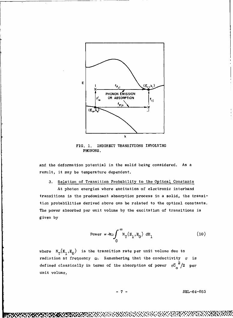

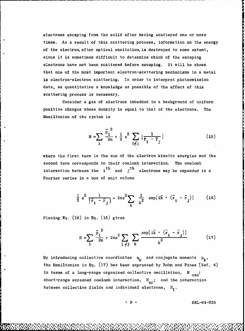

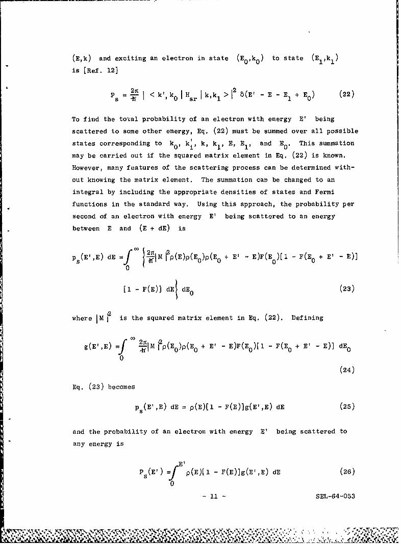


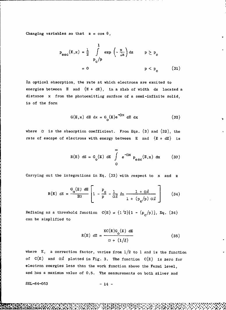


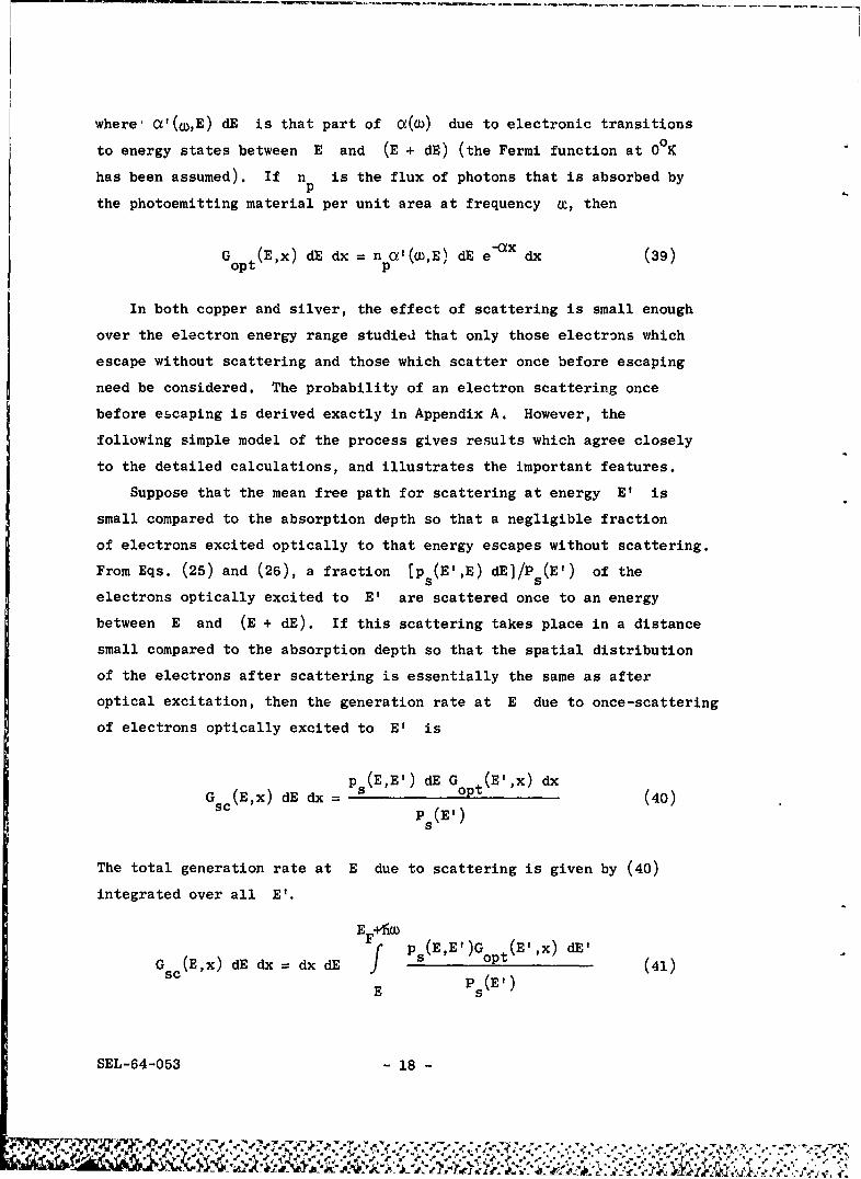


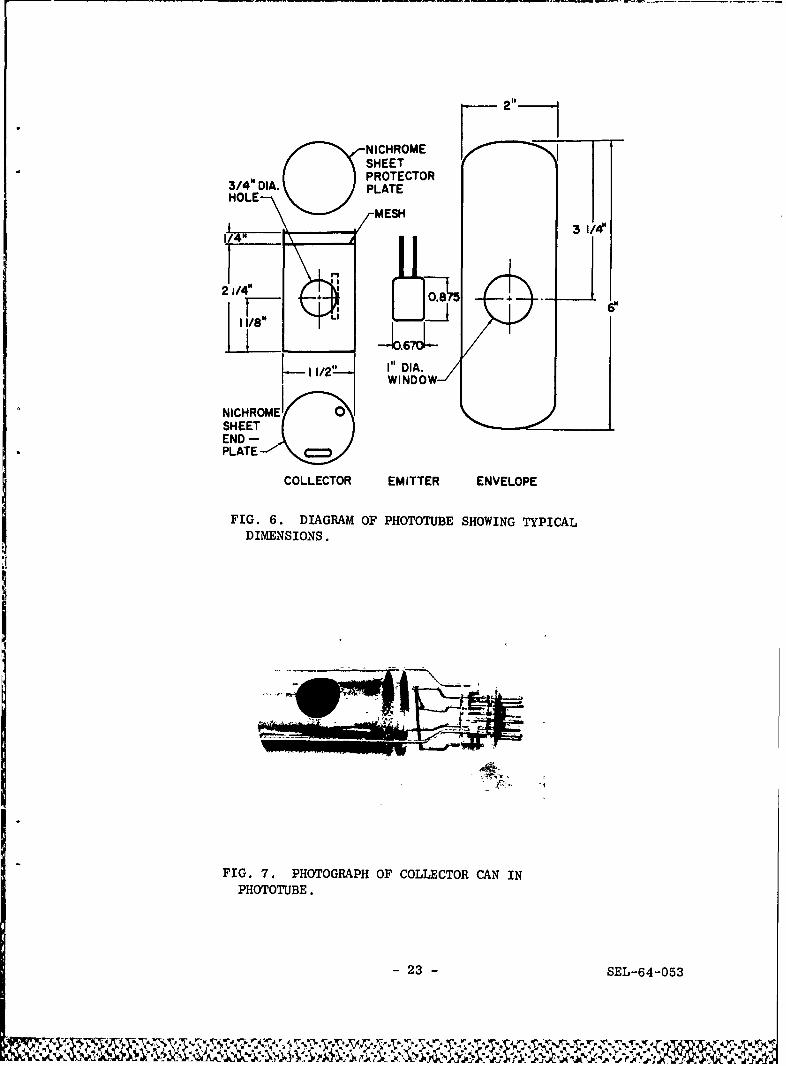


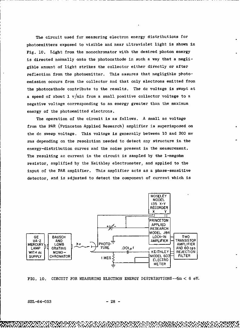


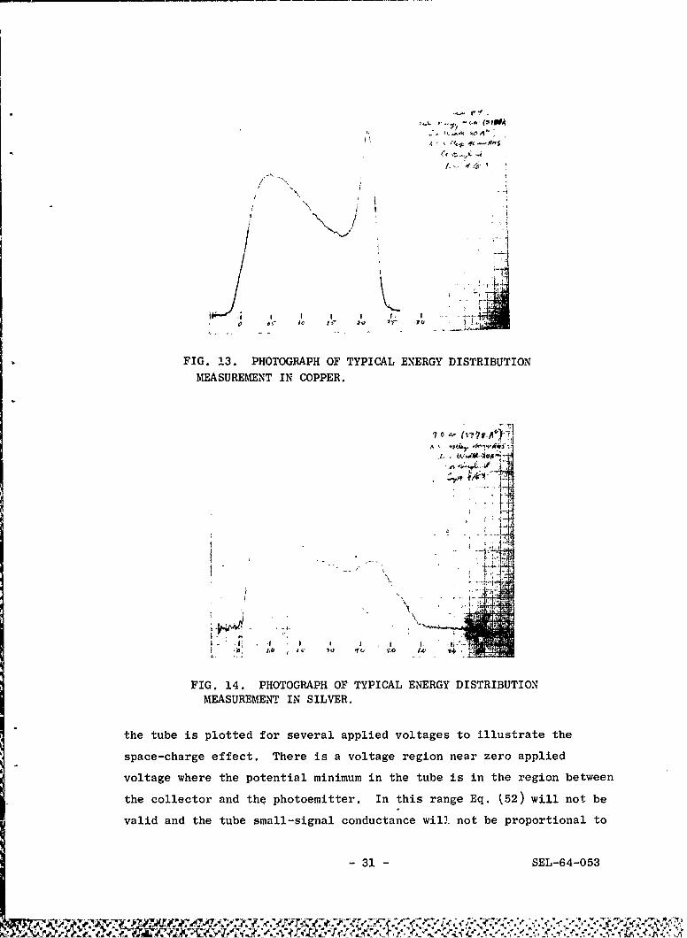
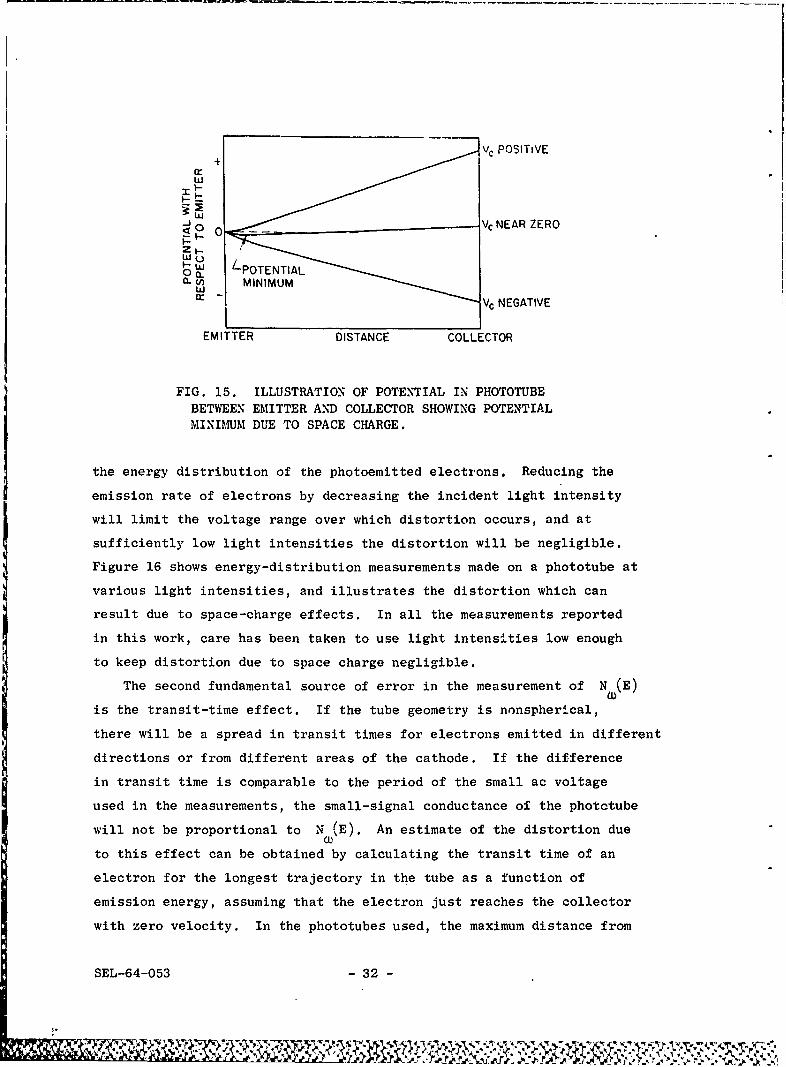


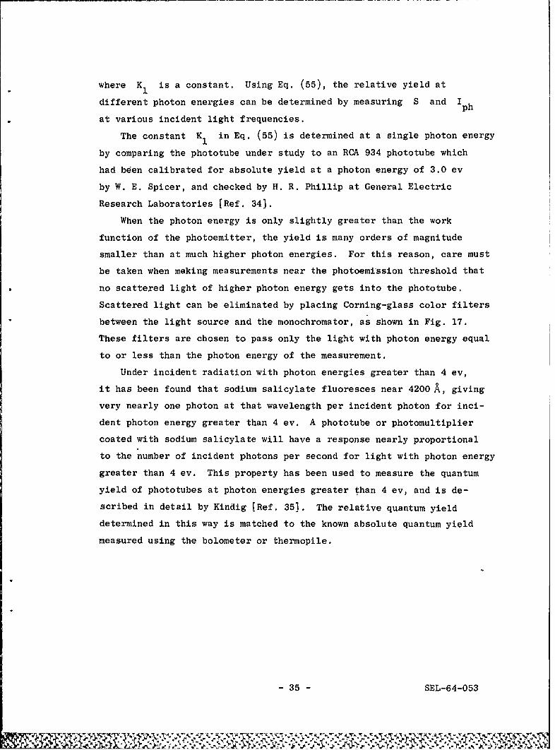


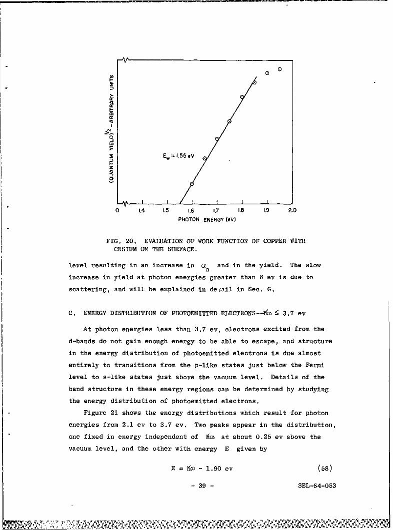


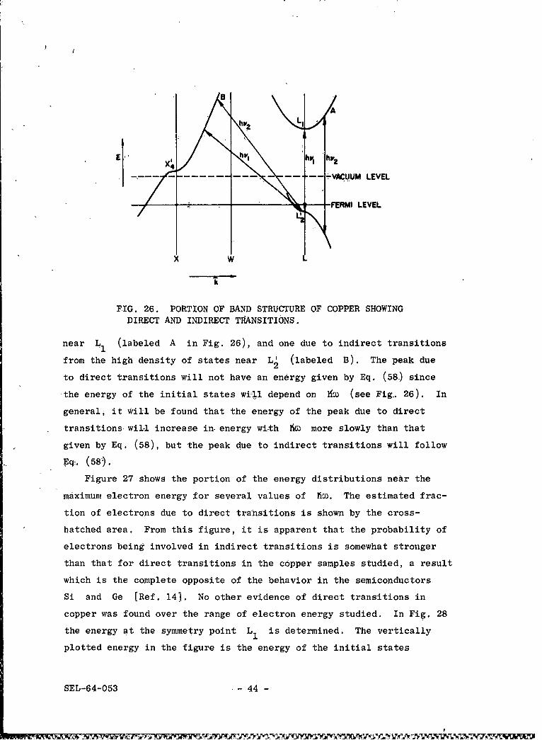
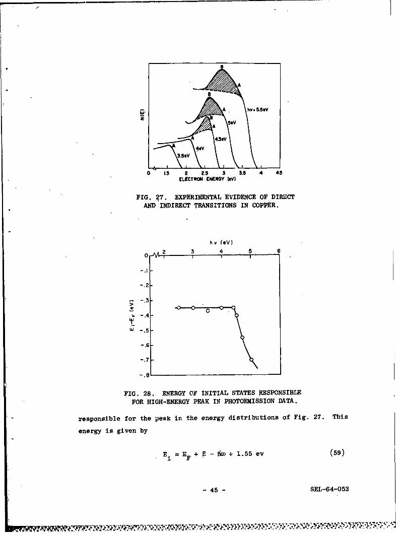


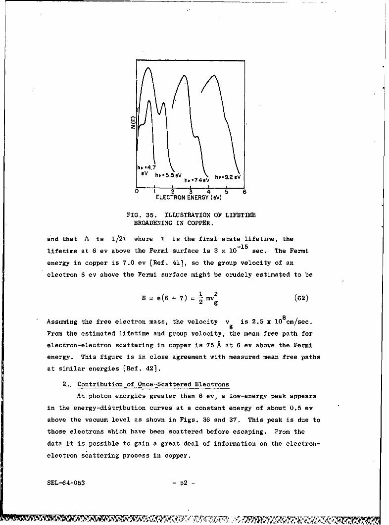
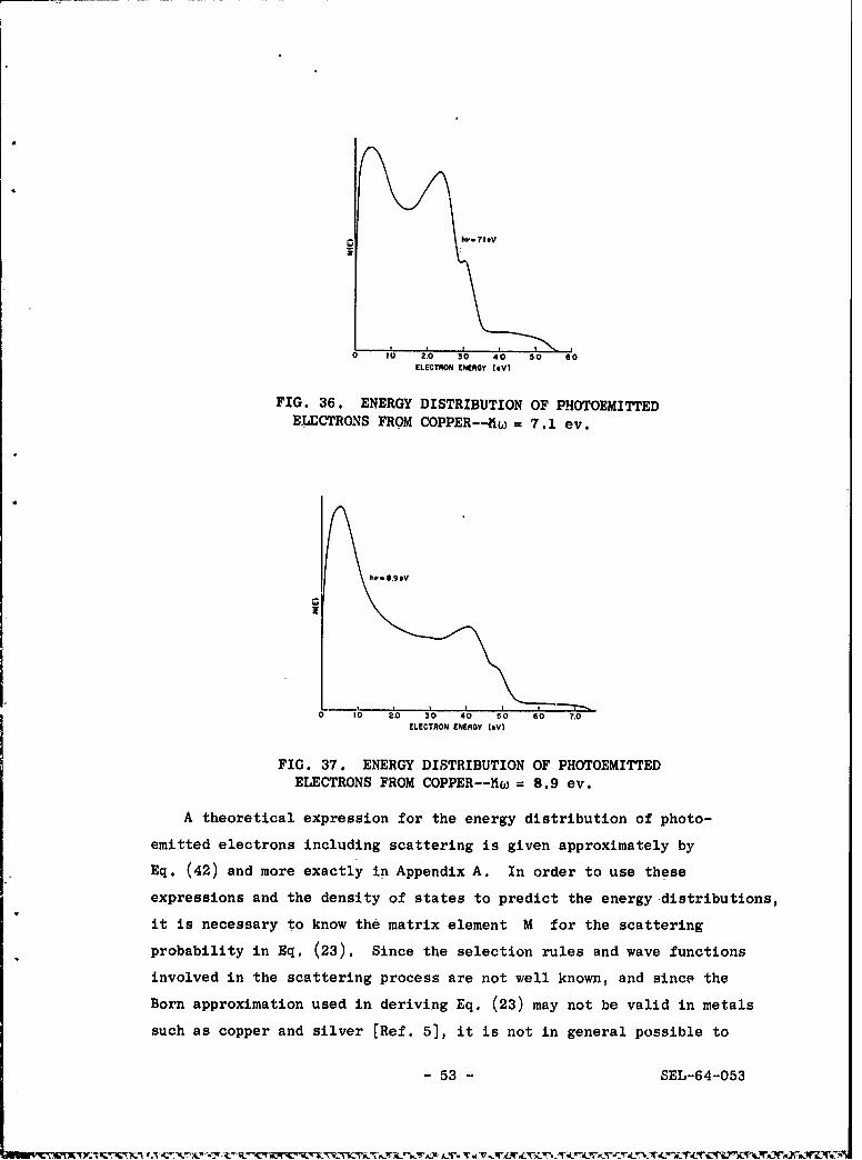


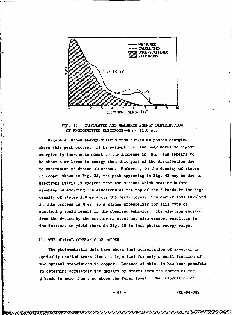
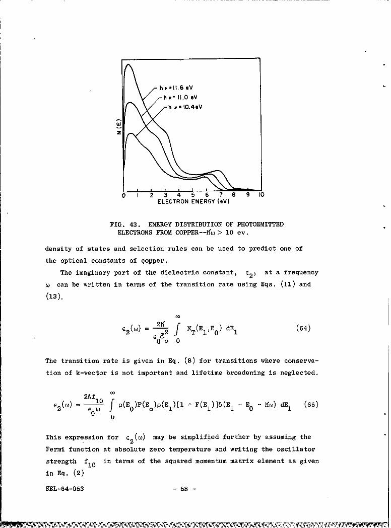

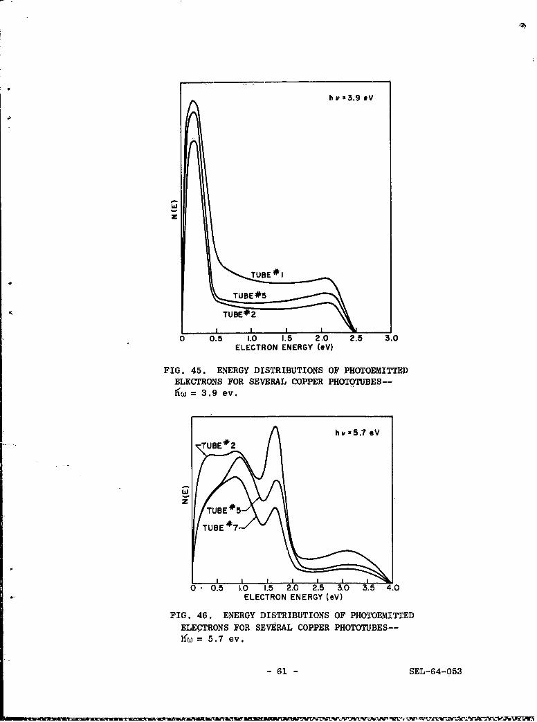
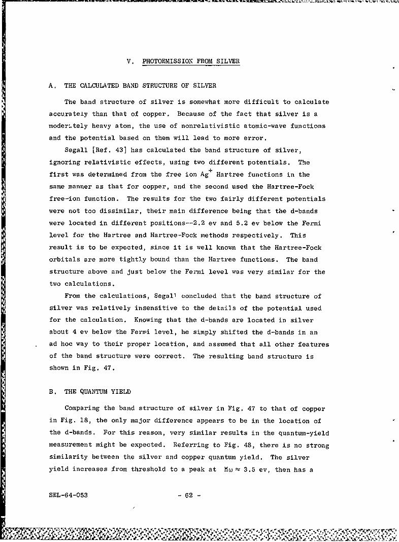

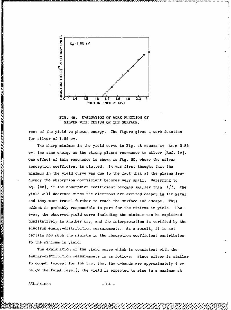


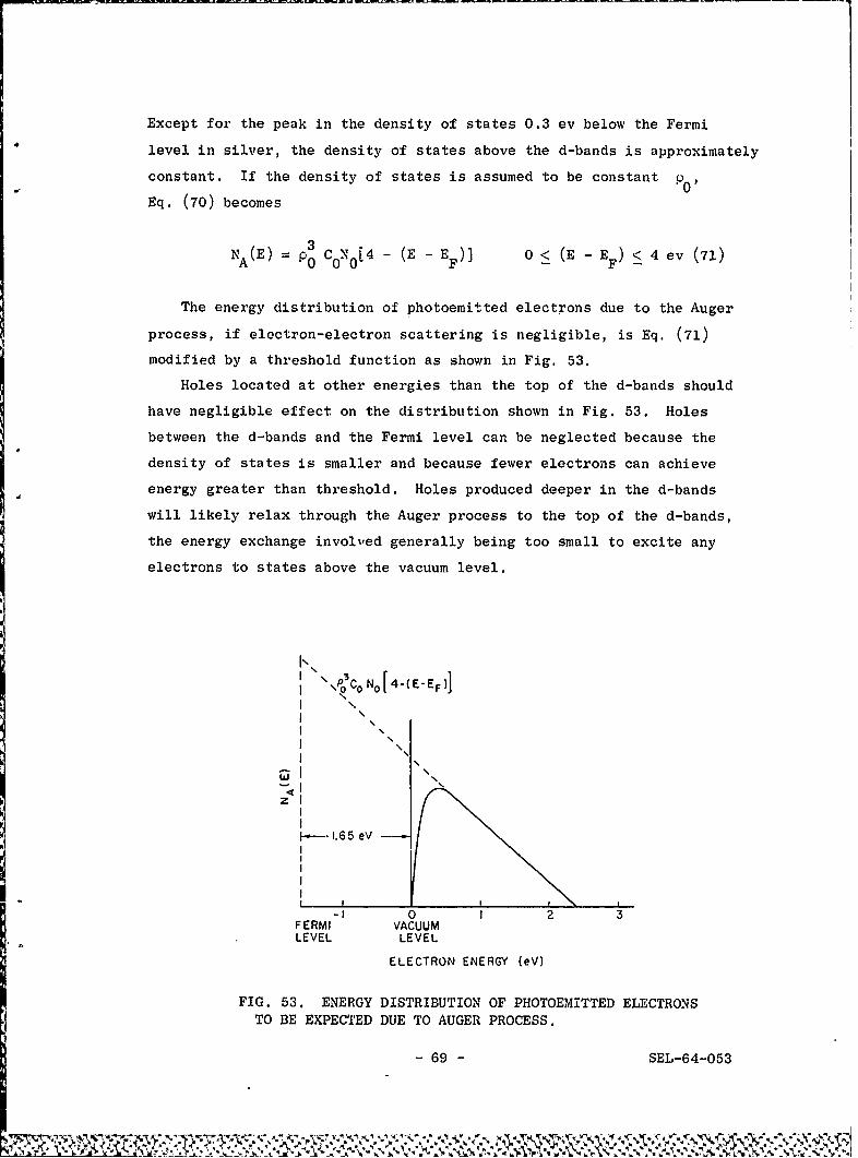


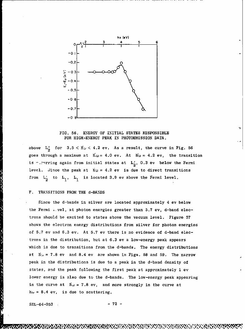
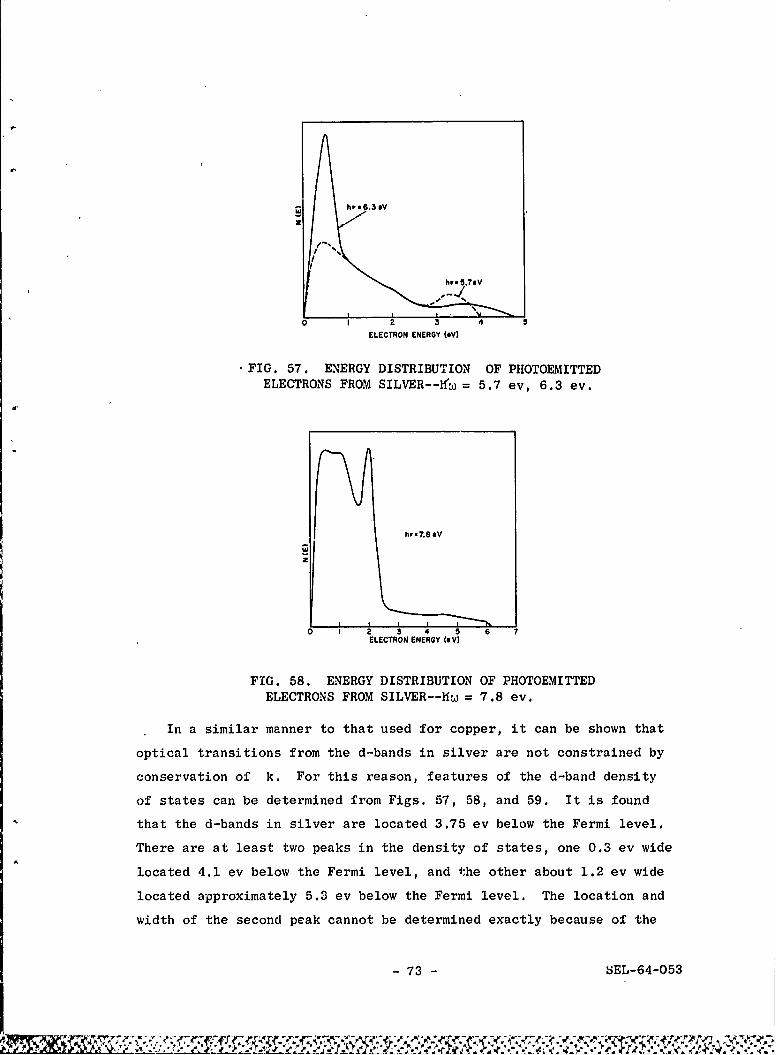
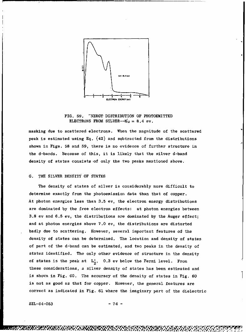

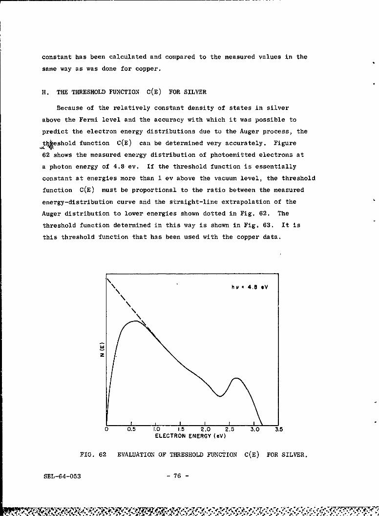


![2013-2014 ANNUAL ASSESSMENT REPORT TEMPLATE...Chart 3 a. PLO 1: j Y b. PLO 1: v Y c. PLO 1: n Y d. PLO 1: te P Y g. LO 3: j Y h. LO 3: l]Y i. PLO 4: al Y) 1 0 0.51 0.51 0 0.51 0.51](https://static.documents.pub/doc/80x56/5f2cb7f173abf20ea42d8e53/2013-2014-annual-assessment-report-template-chart-3-a-plo-1-j-y-b-plo-1.jpg)


