Structure and growth mechanism of ZnSe nanowires Joysurya Basu, R. Divakar, Julia Nowak, Stephan Hofmann, Alan Colli et al. Citation: J. Appl. Phys. 104, 064302 (2008); doi: 10.1063/1.2977722 View online: http://dx.doi.org/10.1063/1.2977722 View Table of Contents: http://jap.aip.org/resource/1/JAPIAU/v104/i6 Published by the American Institute of Physics. Related Articles High pressure phase transition of ZnO/SiO2 core/shell nanospheres J. Appl. Phys. 113, 054314 (2013) Nonlinear bleaching, absorption, and scattering of 532-nm-irradiated plasmonic nanoparticles J. Appl. Phys. 113, 053107 (2013) Optimal conditions for magnetization reversal of nanocluster assemblies with random properties J. Appl. Phys. 113, 043902 (2013) Surface plasmon enhanced photoluminescence and Raman scattering of ultra thin ZnO-Au hybrid nanoparticles J. Appl. Phys. 113, 033512 (2013) On the dynamics of Cu ions injection into low-k nanoporous materials under oscillating applied fields J. Appl. Phys. 113, 034104 (2013) Additional information on J. Appl. Phys. Journal Homepage: http://jap.aip.org/ Journal Information: http://jap.aip.org/about/about_the_journal Top downloads: http://jap.aip.org/features/most_downloaded Information for Authors: http://jap.aip.org/authors Downloaded 07 Feb 2013 to 129.169.173.162. Redistribution subject to AIP license or copyright; see http://jap.aip.org/about/rights_and_permissions
Transcript
Structure and growth mechanism of ZnSe nanowiresJoysurya Basu, R. Divakar, Julia Nowak, Stephan Hofmann, Alan Colli et al. Citation: J. Appl. Phys. 104, 064302 (2008); doi: 10.1063/1.2977722 View online: http://dx.doi.org/10.1063/1.2977722 View Table of Contents: http://jap.aip.org/resource/1/JAPIAU/v104/i6 Published by the American Institute of Physics. Related ArticlesHigh pressure phase transition of ZnO/SiO2 core/shell nanospheres J. Appl. Phys. 113, 054314 (2013) Nonlinear bleaching, absorption, and scattering of 532-nm-irradiated plasmonic nanoparticles J. Appl. Phys. 113, 053107 (2013) Optimal conditions for magnetization reversal of nanocluster assemblies with random properties J. Appl. Phys. 113, 043902 (2013) Surface plasmon enhanced photoluminescence and Raman scattering of ultra thin ZnO-Au hybrid nanoparticles J. Appl. Phys. 113, 033512 (2013) On the dynamics of Cu ions injection into low-k nanoporous materials under oscillating applied fields J. Appl. Phys. 113, 034104 (2013) Additional information on J. Appl. Phys.Journal Homepage: http://jap.aip.org/ Journal Information: http://jap.aip.org/about/about_the_journal Top downloads: http://jap.aip.org/features/most_downloaded Information for Authors: http://jap.aip.org/authors
Downloaded 07 Feb 2013 to 129.169.173.162. Redistribution subject to AIP license or copyright; see http://jap.aip.org/about/rights_and_permissions
Structure and growth mechanism of ZnSe nanowiresJoysurya Basu,1,a� R. Divakar,2 Julia Nowak,3 Stephan Hofmann,4 Alan Colli,5 A. Franciosi,and C. Barry Carter1
1Department of Chemical, Materials and Biomolecular Engineering, 191 Auditorium Road,University of Connecticut, Storrs-06269, Connecticut, USA2Physical Metallurgy Division, Indira Gandhi Centre for Atomic Research, Kalpakkam-603102, TN, India3Department of Chemical Engineering and Materials Science, 421 Washington Ave. SE,University of Minnesota, Minneapolis-55455, Minnesota, USA4Electrical Engineering Division, University of Cambridge, 9 JJ Thompson Avenue,Cambridge CB3 0FA, United Kingdom5Laboratorio Nazionale TASC-INFM, Area Science Park, 34012 Trieste, Italy
�Received 16 April 2008; accepted 11 July 2008; published online 18 September 2008�
So-called one-dimensional structures of compound semi-conductors, such as nanowires, nanobelts, and nanosaws, arenow of significant research interest because of their potentialapplications in nanoscale electronics and photonics.1–3 ZnSeis an important II-VI semiconductor because of its suitabilityfor short-wavelength optoelectronic devices.4 Successful ap-plication of a device is critically dependent on its structureand on any interfaces created during the growth.5 Cost-effective application can only be realized if the nanostruc-tures are self-assembled, which requires a clear understand-ing of the growth mechanism. ZnSe-nanowire growth byvapor-phase deposition �CVD�, metalorganic chemical-vapordeposition �MOCVD�, molecular-beam epitaxy �MBE�, andthermochemical processes at various growth temperatureshas been reported. MBE is currently the technique of choicebecause ZnSe-based lasers with good performance and longlifetime can be produced with material grown by thistechnique.6 Widely varied growth temperatures from 300 °Cto 530 °C have been reported for this nanowire.6,7 ZnSe-nanowire growth at 1250 °C by thermochemical process hasbeen reported.8 Hydrothermal synthesis of other metal-selenide nanowire has also been reported.9
The first ever wirelike morphology in metallic and ce-ramic systems was observed more than half a centuryago10,11 and the growth mechanism of this particular mor-phology was proposed more than four decades ago.12 How-ever, the structure and defects are still not totally understood
and the growth mechanism is debated. There are examples inwhich existing proposals for growth mechanisms fail to ex-plain the experimental evidence and there is no definite prooffor the new proposed growth mechanisms.
Gold nanoparticles are the most frequently used catalystsfor ZnSe-nanowire growth though Zn-catalyzed growth ofZnSe nanowires has also been reported.8 Irrespective of thegrowth temperature, it has been assumed that the catalyst isin the liquid state, and that the wires grow by the well-knownVLS growth mechanism.12 The alternative is that the mecha-nism does not involve a liquid-phase.6,13 According to thisVSS model, solid catalytic nanoparticles are exposed to thevapor phase; diffusion of the nanowire material through thenanoparticle then leads to nanowire growth. This theory doesnot require the existence of a eutectic temperature or heatingof the particle above the eutectic temperature. However, thistheory does not explain at present why the nanowire mor-phology develops rather than other possible morphologies.
It is envisaged that in the near future nanowires will bean indispensable component of nanoelectronic devices.4 It isalso recognized that the electronic properties of such nano-wires are very sensitive to the structure, defects, and inter-faces. There are very few reports on structural defects4 andinterfaces in nanowires. It has been widely reported in theliterature that the nanowire diameter is controlled by the sizeof the catalyst. It has also often been observed that the nano-wire tapers from the base toward the tip. This taperingclearly suggests a decrease in the volume of the catalyticparticles during growth but there is no definite proof as towhere the catalyst is lost during growth.
In the present work, ZnSe nanowires grown by MBEa�Electronic mail: [email protected].
have been studied in order to understand the structure, de-fects, interfaces, and growth mechanism of the nanowire.The important observations of this work can be summarizedto give further understanding of the nanowire growth mecha-nism.
II. EXPERIMENTAL TECHNIQUES
ZnSe nanowires were grown onto 300-mesh Mo trans-mission electron microscopy �TEM� grids by solid-sourceMBE. A 20-nm-thick SiO2 layer was initially sputtered onthe grid prior depositing a thin �0.5–2 nm� Au catalyst layer.Elemental Zn and Se were evaporated on the grid for 1 h,while the substrate temperature was kept at 450 °C, as mea-sured by an infrared pyrometer. The Se flux was fixed for allsamples, whereas the Zn flux was varied to achieve differentZn/Se beam pressure ratios �BPRs�. Details of the processingparameters have been reported elsewhere.6,7 As-grown nano-wires, the structure of the catalyst particles and the morphol-ogy of these particles were characterized using a Tecnai T12TEM operated at 120 kV; a Tecnai G2 F30 TEM operated at300 kV was used for high-resolution and composition char-acterization. Scanning transmission electron microscopy�STEM� and high-angle annular-detector dark-field imaging�HAADF� were used to observe the nanowires under mass-thickness contrast in order to detect any elemental segrega-tion. In order to observe possible growth of the nanowires,two in situ heating-stage studies were conducted using a Ga-tan double-tilt heating holder. The nanowires were heatedfrom room temperature to 600 °C at a heating rate of1 °C /min; samples were stabilized at 100 °C intervals.
While heating, images were recorded continuously at inter-vals of 1.65 s. In one study, one nanowire tip was observedcontinuously; in a second study a number of tips were ob-served concurrently. After heating, the nanowires were char-acterized as described above in order to obtain post heatinginformation.
III. RESULTS
TEM images of the ZnSe nanowires grown by MBEtechnique with different growth parameters are shown inFigs. 1�a� and 1�b�. The BPRs used for samples �Fig. 1�a�and 1�b�� were 2.5 and 0.4, respectively. The nanowires inFig. 1�a� were grown under Zn-rich conditions, whereasnanowires in Fig. 1�b� were grown under Se-rich conditions.It can be seen that the nanowire morphology is very sensitiveto the growth parameters involved. In Fig. 1�a� the nanowiresare almost 80 nm wide at the base and about 30–40 nm wideat the tip and the wires are more than 1 �m long. The wiresare often bent and one side of the wires is not smooth mak-ing these more similar to the nanosaw morphology. A 30–40nm sized catalyst particle can be observed at the end of eachnanowire. These catalyst particles are irregular in shape. Themorphology of the nanowires in Fig. 1�b� is different. Thewires are longer than in Fig. 1�a�; they are less tapered andthe undulation on the surface is not present. Though at the tipof each nanowire, a catalytic gold particle is observed, eachparticle is almost spherical and about 20 nm in diameter.Electron diffraction �Fig. 1 inset� from these samples indi-cates that the nanowires have the hexagonal wurtzite struc-ture as observed in the selected area diffraction patterns witha lattice parameter very close to the reported value for thebulk material. However, the cubic polymorph of ZnSe hasvery similar d spacings. A detailed analysis of the diffractionpatterns is given in Table I. It is observed that a number ofDebye rings are present in the diffraction pattern, whichwould not have been present for cubic ZnSe. This shows thatthe nanowires are primarily hexagonal in structure but thatthe cubic polymorph could also be present. A brief compari-son of the two types of nanowires suggests that the nano-wires in Fig. 1�a� are relatively more tapered than those inFig. 1�b�.
A montage of enlarged images of one of the nanowiresin Fig. 1�a� �sample grown under a Zn-rich environment� isgiven in Fig. 2. At higher magnification, a 3–5 nm thickamorphous layer can be seen at the nanowire body. A numberof fringes running along the length of the nanowire body and
FIG. 1. TEM micrographs of ZnSe nanowires grown by MBE under �a�Zn-rich �b� Se-rich condition. Catalyst Au particles can be seen at the tip ofthe nanowires and the morphology of the nanowires varies with the growthparameters. The typical diffraction patterns from the nanowires �inset�matches with hexagonal �hP4� structure. However, this does not rule out thepossibility of the existence of the cubic polymorph.
TABLE I. Analysis of the diffraction patterns in Fig. 1�inset�
064302-2 Basu et al. J. Appl. Phys. 104, 064302 �2008�
Downloaded 07 Feb 2013 to 129.169.173.162. Redistribution subject to AIP license or copyright; see http://jap.aip.org/about/rights_and_permissions
a few short fringes in the transverse direction, spread irregu-larly over the length of the nanowire can be observed. Thiscontrast arises from defects present in the nanowire body.The catalytic tip is irregular and flowerlike in shape. Thisshape is due to the presence of unreacted ZnSe at the tip ofthe nanowire.
High-resolution TEM images of the catalyst tip fromboth types of sample are shown in Figs. 3�a�–3�c�. The mi-crographs in Figs. 3�a� and 3�b� are from the sample shownin Fig. 1�a� �sample grown under a Zn-rich environment�; theremaining image is from the sample shown in Fig. 1�b��sample grown under a Se-rich environment�. The latticefringes observed in Figs. 3�a� and 3�b� closely match withZnSe, indicating a definitive presence of unreacted ZnSe atthe nanowire tip. In Figs. 3�a� and 3�b� lattice fringe of simi-lar spacing can be observed in various directions. This indi-cates that the unreacted ZnSe is polycrystalline in naturethough the boundary between the crystals cannot be clearlyresolved. The polycrystalline grains are 5–10 nm in size anda 3–5 nm thick amorphous layer surrounds the catalytic tip.In comparison to Figs. 3�a� and 3�b� the nature of the catalysttip in Fig. 3�c� is different. In the high-resolution image the dspacing matches with FCC gold. The catalyst is 2–3 nm in
size and it is spherical in shape. It can be concluded that inthe nanowires shown in Fig. 1�a�, unreacted ZnSe is presentwhereas in the other sample it is barely detectable. The ex-tent of the completeness of the reaction leads to a change inthe shape of the nanowire tip.
A high-resolution TEM image of the body of a nanowirein Fig. 1�b� �sample grown under a Se-rich environment� isshown in Fig. 4. Lattice fringes with a 3.22 Å spacing canbe observed. These fringes may be associated with either the0002 planes of wurtzite ZnSe or the 111 planes of cubicZnSe. These planes are perpendicular to the direction ofnanowire growth. As only one set of lattice fringes could beresolved for this nanowire, the growth direction could not bedetermined with certainty. In this image no lattice defect canbe observed in the nanowire body; a 1–2 nm thick amor-phous layer can be observed enclosing the nanowire body. Ahigh-resolution TEM image of a nanowire body in Fig. 1�a��sample grown under a Zn-rich environment� is given in Fig.5. As it has been mentioned earlier, these nanowires are�80 nm thick at the base and �30 nm thick at the tip.High-resolution imaging through a thickness of 80 nm is notexpected to yield a very good lattice image. Moreover, as thewires are grown onto a TEM grid, their mechanical stability
FIG. 2. TEM montage image of ZnSe nanowire grown under Zn-rich con-dition. The nanowire tapers toward the tip. The shape of the tip is irregularand a number of defects can be seen at the nanowire body.
FIG. 3. High-resolution electron micrographs of the ZnSe nanowire tip. �a� The tip is irregular in shape with unreacted ZnSe and an amorphous layer. �b� Theunreacted ZnSe is polycrystalline in nature �c� After the total transformation of ZnSe, the almost spherical Au catalyst can be observed at the nanowire tip.
FIG. 4. High-resolution electron micrograph of the nanowire body. Theplanes perpendicular to the nanowire growth direction are imaged and a 1–2nm thick amorphous layer can be observed at the nanowire body.
064302-3 Basu et al. J. Appl. Phys. 104, 064302 �2008�
Downloaded 07 Feb 2013 to 129.169.173.162. Redistribution subject to AIP license or copyright; see http://jap.aip.org/about/rights_and_permissions
also affects image quality; the nanowires tend to vibrate.However, in some parts of the image cross-fringe patterncould be observed. Analysis of the pattern reveals that thenanowire is cubic in structure and the wire is oriented ap-proximately along the 110 zone axis. Several 111 twin planescould be observed. Such twin boundaries are the most com-monly occurring defects in this nanowire. This further con-firms that cubic ZnSe phase is also present in the sample.The twins are the origin of the elongated fringelike contrastin the Fig. 2.
A STEM �scanning TEM� image and HAADF image ofa nanowire shown in Fig. 1�a� �sample grown under a Zn-rich environment�, are given in Figs. 6�a� and 6�b�, respec-tively. In the micrograph the usual tapered nature of thenanowire can be observed. Additionally, a few dark patchesin the STEM image and corresponding bright patches in theHAADF image can be observed. The contrast mechanism inthe STEM and HAADF images and corresponding composi-tion maps suggest that the contrast arises from the presenceof gold particles along the nanowire body. The particles areirregular in shape and their size may range up to 20 nm.
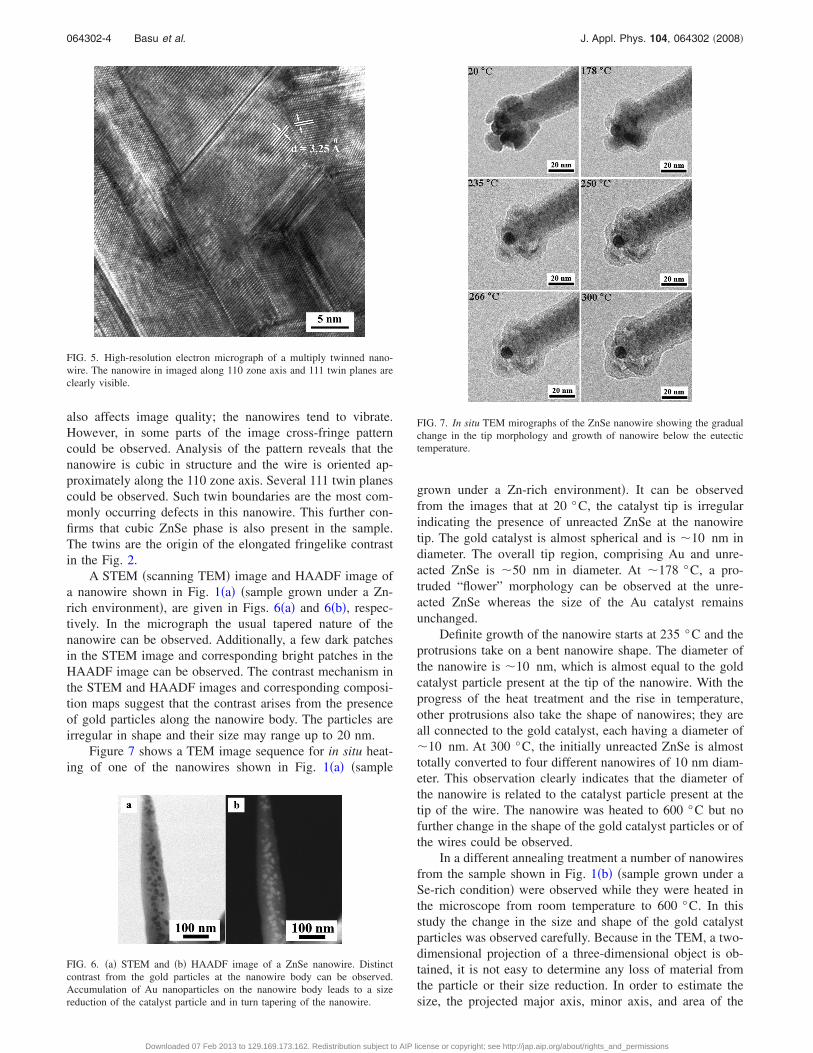
Figure 7 shows a TEM image sequence for in situ heat-ing of one of the nanowires shown in Fig. 1�a� �sample
grown under a Zn-rich environment�. It can be observedfrom the images that at 20 °C, the catalyst tip is irregularindicating the presence of unreacted ZnSe at the nanowiretip. The gold catalyst is almost spherical and is �10 nm indiameter. The overall tip region, comprising Au and unre-acted ZnSe is �50 nm in diameter. At �178 °C, a pro-truded “flower” morphology can be observed at the unre-acted ZnSe whereas the size of the Au catalyst remainsunchanged.
Definite growth of the nanowire starts at 235 °C and theprotrusions take on a bent nanowire shape. The diameter ofthe nanowire is �10 nm, which is almost equal to the goldcatalyst particle present at the tip of the nanowire. With theprogress of the heat treatment and the rise in temperature,other protrusions also take the shape of nanowires; they areall connected to the gold catalyst, each having a diameter of�10 nm. At 300 °C, the initially unreacted ZnSe is almosttotally converted to four different nanowires of 10 nm diam-eter. This observation clearly indicates that the diameter ofthe nanowire is related to the catalyst particle present at thetip of the wire. The nanowire was heated to 600 °C but nofurther change in the shape of the gold catalyst particles or ofthe wires could be observed.
In a different annealing treatment a number of nanowiresfrom the sample shown in Fig. 1�b� �sample grown under aSe-rich condition� were observed while they were heated inthe microscope from room temperature to 600 °C. In thisstudy the change in the size and shape of the gold catalystparticles was observed carefully. Because in the TEM, a two-dimensional projection of a three-dimensional object is ob-tained, it is not easy to determine any loss of material fromthe particle or their size reduction. In order to estimate thesize, the projected major axis, minor axis, and area of the
FIG. 5. High-resolution electron micrograph of a multiply twinned nano-wire. The nanowire in imaged along 110 zone axis and 111 twin planes areclearly visible.
FIG. 6. �a� STEM and �b� HAADF image of a ZnSe nanowire. Distinctcontrast from the gold particles at the nanowire body can be observed.Accumulation of Au nanoparticles on the nanowire body leads to a sizereduction of the catalyst particle and in turn tapering of the nanowire.
FIG. 7. In situ TEM mirographs of the ZnSe nanowire showing the gradualchange in the tip morphology and growth of nanowire below the eutectictemperature.
064302-4 Basu et al. J. Appl. Phys. 104, 064302 �2008�
Downloaded 07 Feb 2013 to 129.169.173.162. Redistribution subject to AIP license or copyright; see http://jap.aip.org/about/rights_and_permissions
catalyst particles have been measured. The change in theprojected length of major axis, minor axis, and the area oftwo different catalyst particles are given in Fig. 8. In bothfigures a gradual decrease of the projected lengths and theprojected area has been observed. The variation that is ob-served in some of the curves can be attributed to the out-of-plane bending of the nanowires leading to a change in theprojected view. In both cases the curves reach the minimumat a temperature just above 200 °C to just below 250 °C.After that the curves become almost parallel to the tempera-ture axis. This observation clearly indicates that the size ofthe catalyst particles also changes in the same temperatureregime where nanowire growth was observed for the othersample. This can be attributed to the diffusion of dissolved
Zn and Se from the catalyst particle. During this in situ heat-ing experiment, any change in contrast in the catalyst particlewas carefully monitored. Within the scanned temperaturerange, any signature of melting of the nanoparticle could notbe detected.
IV. DISCUSSION
It has been observed in this work that nanowire mor-phology is extremely sensitive to the processing parameters.The two different nanowire samples studied in the presentwork are morphologically very different because of the dif-ference in the processing parameters. In the samples bothhexagonal and cubic polymorphs of ZnSe are present. In the
FIG. 8. �Color online� Gradual decrease in the projected major axis, minor axis, and the area of the catalytic tips of two different nanowires as observed duringin situ heating.
064302-5 Basu et al. J. Appl. Phys. 104, 064302 �2008�
Downloaded 07 Feb 2013 to 129.169.173.162. Redistribution subject to AIP license or copyright; see http://jap.aip.org/about/rights_and_permissions
nanowires grown under Zn-rich condition �Fig. 1�a��, unre-acted ZnSe is present at the tip along with the gold catalyst.In this case the tip is larger in size and is irregular in shape.In the nanowires grown under Se-rich condition �Fig. 1�b��,the gold catalysts are smaller in size and regular in shape. Inthese nanowires, unreacted ZnSe cannot be observed at thenanowire tip. It can be concluded from this observation thatSe-rich conditions yield good-quality nanowires, whereasZn-rich conditions lead to tapered and very defectednanosaw type morphology. The irregular flower-shaped tipsalso form under Zn-rich conditions only. Philipose et al.14
have reported that Zn-rich conditions result in a better struc-tural and optical quality of ZnSe nanowire, compared to theSe-rich conditions. In this study the trend seems to be in-verted. Philipose et al.14 used vapor-phase growth in Ar at650 °C, in this case nanowires were grown by MBE invacuum at 450 °C. At low growth temperatures, therefore,the trend seems to be inverted.
A very thin amorphous layer can be observed around thenanowire body and the tip in both the samples. The presenceof a thin amorphous layer at the nanowire body has beenreported by Hofmann et al.15 Such a layer has been attributedto the formation of a native oxide film on the surface of thenanowire. In the present work occasionally amorphous layerhas been observed but buildup of an amorphous layer at thenanowire body has not been observed to occur with in-creased exposure of the sample to the electron beam. Thesurface structure of the wires is also dependent on the growthparameters. In one case the surface is undulated makingthese wires more similar to the nanosaws; in other case thenanowires are straight and their surfaces are flat. Undulationat the nanowire surface has often been attributed to migrationof the gold catalyst to the nanowire body, where it then actsas a catalyst for an individual secondary nanowire growth.16
Kodambaka et al.17 have also reported that the nanowiregrowth morphology and kinetics are sensitive to the growthparameters and that the electron beam has no effect on Sinanowire growth. The most commonly observed growth de-fects are twin boundaries. The presence of periodicallyspaced twin boundaries has been reported by Li et al.�2004�.4 For the case of cubic ZnSe nanowires a linear rela-tionship between the nanowire diameter and the periodicspacing of the twin boundaries was reported. Twin formationis generally associated with the decrease in elastic strain en-ergy at the surface of the nanowire. Such growth defects mayhave important consequences on the electronic properties ofthese wires.
It has been reported in earlier literature that the diameterof the nanowires strongly correlates to the size of the catalystparticles present at the tip of the wire.18,19 It has also beenpostulated that the minimization of surface free energy be-tween the liquid catalyst droplet and the growing crystalplanes determines the nanowire growth direction. Often, forvery small diameter, nanowire growth direction is deter-mined by the surface energy of the nanowire. Following thiscriteria, cubic and hexagonal ZnSe nanowires grow in the111 and 0001 directions, respectively.4 In the present study,the cubic and hexagonal forms of ZnSe have been observed,although growth of cubic ZnSe nanowire in several direc-
tions has been reported previously.20 In many cases the nano-wires taper while they grow strongly indicating a loss ofcatalyst material during growth. In this work gold nanopar-ticles have been observed at the nanowire body and theirchemical identity has been confirmed by EDS analysis. Ka-mins et al. �2001� have shown by EDS that the Ti clusterssegregated along the Si nanowire body during growth.21
Kodambaka et al. �2006� have speculated that incorporationof the Au catalyst at the nanowire body during the nanowiregrowth leads to tapering.22 They have also reported that theincorporation of oxygen during nanowire growth produces athin layer of oxide, which modifies the mobility of the cata-lyst resulting in uniformity in the diameter of the nanowire.Supersaturation of the adsorbed atoms and the importance ofsurface diffusion for different other elemental and compoundnanowires have been reported in literature.23,24 It can be con-cluded from this observation that during nanowire growth,gold nanoparticles are distributed randomly on the nanowirebody leading to a decrease in the catalyst particle size. As thenanowire diameter is strongly related to the catalyst particlesize at the top, nanowires also taper while they grow.
The VLS mechanism is the most widely accepted growthmechanism. It is assumed that a catalyst nanoparticle assiststhe growth and controls of the diameter of the nanowire.Above a certain temperature the catalytic nanoparticle be-comes liquid and it is exposed to the vapor of the growingnanowire material. The nanowire material slowly dissolvesinto the nanoparticle and when it becomes supersaturated,following continuous exposure of the nanowire material, sol-ute partitioning and rejection of the solute takes place fromother side of the liquid droplet leading to nanowire growth.
The inherent assumption is that there must be a eutecticbetween the catalytic nanoparticle and nanowire material.This is required to take the pure catalytic nanoparticle abovethe melting temperature and then as the nanowire materialstarts dissolving, it should be possible to maintain the liquidstate even at a lower temperature. This theory does not ex-plain why solute partitioning takes place only from the otherside leading to a nanowire growth and not to a particle witha different core. The development of this particular morphol-ogy may be explained from the structural anisotropy of thecrystal. A schematic of nanowire growth by the VLS mecha-nism is given in Fig. 9. Nanowire growth has been observedbelow the eutectic temperature19,25 suggesting that the cata-lyst particle is not in the molten state; a composition analysisof the catalyst tip after growth termination at various stagesindicates that the nanowire growth may occur while the cata-lyst particle is in the solid state.13 The computational modelin support of this growth mechanism fits very well with theexperimental observations. Kamins et al. �2001� have shownthat Si nanowire growth is possible below the melting tem-
FIG. 9. �Color online� Schematic of the VLS growth mechanism ofnanowire.
064302-6 Basu et al. J. Appl. Phys. 104, 064302 �2008�
Downloaded 07 Feb 2013 to 129.169.173.162. Redistribution subject to AIP license or copyright; see http://jap.aip.org/about/rights_and_permissions
perature of TiSi2 by solid-state diffusion of Si.21 The diffu-sivity of Si along the surface and nanoparticle body matchesvery well with the nanowire growth rate observed in thatwork. It has been proposed that the catalytic action of Ti isinvolved in the decomposition of the Si containing precursorgas and that the resulting product takes the wire shape inorder to avoid generating additional interface. Systematicheat treatments and compositional analysis of the catalystparticle in Au-assisted InAs nanowire growth by MOVPEshows that InAs nanowire growth is possible far below theeutectic temperature. All the related evidence indicates thatthe nanowires grew by solid-state diffusion through the Aucatalyst particle.26 The question that may be asked at thispoint is then how the Au thin film evolved into nanoparticleswhile nanowires grew. Although this is not the primary focusof the paper, solid-state dewetting is widely reported inliterature.27 Contrary to this Wu and Yang �2001� haveshown by an in situ heating experiment that Ge vapor dis-solves into a liquid Au catalyst and then, due to super-saturation nucleates Ge nanowires from liquid Au.28 The heattreatment in that study was carried out at 900 °C in vacuum.
In other studies of the nanowire growth mechanism ithas been reported that the Au catalyst was in a liquid statethough the growth took place at a temperature significantlybelow the melting temperature of gold.20 One possible originof melting point depression is the Gibbs–Thompson effectwhich results from the finite size and surface energy of thecrystal.29 A calculation for a pure gold crystal of 40 nm di-ameter shows that a melting point depression of 60–65 °C ispossible.30 A melting point depression of few hundred de-grees is unreasonable for gold nanoparticles. The meltingand solidification behavior of other metallic nanoparticles inembedded systems indicates that the melting point dependson thermal history, interfacial energy and many other param-eters, which are not totally understood. Although meltingpoint depression of several hundred degrees has not beenreported.31–37 Recent in situ environmental microscopy workby Kodambaka et al.38 shows that the physical state of thenanoparticle depends on various parameters. The size of thecatalyst, the pressure of the gas inside the microscope, thesupersaturation, and the degree of undercooling all have astrong influence on the physical state of the catalyst particle.These authors did not observe an electron-beam effect on thephysical state of the particle. They have shown that Ge nano-wire growth is possible with both solid and liquid Au catalystparticles.38 Hofmann et al.39 have proved beyond ambiguitythat Si nanowire growth is possible with a solid catalyst par-ticle.
In situ experiments carried out in the course of thepresent work definitely indicates that nanowire growth ispossible below the eutectic temperature when the catalystparticle is in the solid state. These experiments were carriedout in the microscope under high-vacuum condition withoutthermal cycling. In this case the effect of gas and thermalundercooling can be ruled out. It has to be understood at thispoint that the growth of nanowire involves kinetic and ther-modynamic interplay. In the present study nanowires grew inthe microscope in the temperature range of 250–300 °C be-cause of the very slow heating rate that was used during the
experiment. With a faster heating rate the nanowires maygrow at a relatively high temperature. It can be easily under-stood that the temperature-composition path followed by thecatalyst particle in VLS and VSS mechanisms are quite dif-ferent. The temperature-composition path followed by thecatalyst particle for VLS and VSS mechanism has been su-perimposed on a binary phase diagram and has been sche-matically presented in Fig. 10. It can be understood from Fig.10 that starting with a pure catalyst particle, the sample mustbe heated so that dissolution of the nanowire materials willstart. At this point the temperature of the alloyed catalystparticle can be kept constant or it may be cooled in such away that it follows the liquidus line. If the temperature iskept constant then after supersaturation nanowire growth willtake place, or if it is cooled down at a steady rate then nano-wire growth will take place at the eutectic temperature. Inanother situation, nanowire material may dissolve into asolid catalyst particle at a moderately high temperature sothat subsequently, at a particular composition, it becomesliquid.
In comparison to this process, in the VSS mechanism thesolid catalyst can be heated up to a sufficiently high tempera-ture so that it may provide a diffusion path for the nanowirematerial. The melting point of Au is 1064.43 °C. MBEgrowth of ZnSe nanowires with Au catalyst takes place at600 °C and the samples in the present study were grown at450 °C. This definitely indicates that the Au nanoparticlenever goes to a liquid state if it remains pure gold. Thispostulate can further be substantiated by phase-diagram in-formation. The ternary phase diagram of Zn-Se-Au is notcomplete but no eutectic reaction has been observed in thebinary vertical section of ZnSe-Au. The Au-Zn phase dia-gram is complicated with a number of binary intermetallics.The only eutectic between Au and Zn occurs at 683 °C withabout 30 at. % Zn. The Au-Se phase diagram is not fullydetermined but the only reported eutectic between Au and Setakes place at 760 °C with 30 at. % Se. For the VLS mecha-nism to be operative, the reaction temperature must be above
FIG. 10. �Color online� Temperature-transformation diagram of �a� VLS and�b� VSS growth mechanisms of nanowire.
064302-7 Basu et al. J. Appl. Phys. 104, 064302 �2008�
Downloaded 07 Feb 2013 to 129.169.173.162. Redistribution subject to AIP license or copyright; see http://jap.aip.org/about/rights_and_permissions
600 °C in order to form the liquid state. The fact that mustbe considered is that at the nanometer scale the contributionof the interfacial energy becomes considerable which mayresult in depression in the melting point and the eutectictemperature,40 however, depression of the order of a hundreddegrees has not been reported. This also indicates the possi-bility that the Au particle is in the solid state. In situ experi-mental observation and available phase-diagram informationstrongly suggests that nanowire growth should be possiblewhile the catalyst particle is in the solid state though it doesnot rule out the possibility of the existence of a VLS mecha-nism.
V. CONCLUSIONS
It can be concluded from the present study that
1� Nanowire morphology is strongly dependent on thegrowth parameters. A thin amorphous layer can be ob-served around the nanowire body and the catalyst par-ticle. Twins are occasionally present at the nanowirebody.
2� Nanowire tips are irregular in shape when unreactedZnSe is present at the tip of the nanowire. UnreactedZnSe is polycrystalline in nature. Catalyst particles arealmost spherical/hemispherical when almost no unre-acted ZnSe is present at the nanowire tip.
3� During growth Au catalyst particles are deposited at thenanowire body causing a size reduction and tapering ofthe nanowire.
4� In the light of the available data and experimental obser-vations it can be concluded that nanowire growth occursby the VSS mechanism in this case.
ACKNOWLEDGMENTS
J. Nowak was supported in part by the IGERT Programof the National Science Foundation under Award NumberDGE-0114372. This study was supported by the 3M HeltzerEndowed Chair and the Proto-IRG seed funding from theUniversity of Minnesota. The authors would like to acknowl-edge stimulating discussion with Dr. Stuart McKernan andthe invaluable assistance of Ms. Janet McKernan. Authorswould like to acknowledge the support by the University ofConnecticut.
1C. B. Carter and M. G. Norton, Ceramic Materials: Science & Engineer-ing �Springer, New York, 2007�, p. 224.
2H. Hasegawa, H. Fujikura, and H. Okada, MRS Bull. 24, 25 �1999�.3K. S. Leschkies, R. Divakar, J. Basu, E. Enache-Pommer, J. E. Boercker,C. B. Carter, U. R. Kortshagen, D. J. Norris, and E. S. Aydil, Nano Lett. 7,1793 �2007�.
4Q. Li, X. Gong, C. Wang, J. Wang, K. Ip, and S. Hark, Adv. Mater.
�Weinheim, Ger.� 16, 1436 �2004�.5J. Basu, J. Deeneen, R. Divakar, S. Hofmann, A. Colli, A. Franciosi, andC. B. Carter, Proceedings of the 16th International Microscopy Congress,2006, Vol. 3, p. 1229.
6A. Colli, S. Hofmann, A. C. Ferrari, C. Ducati, F. Martelli, S. Rubini, S.Cabrini, A. Franciosi, and J. Robertson, Appl. Phys. Lett. 86, 153103�2005�.
7A. Colli, A. Fasoli, S. Hofmann, C. Ducati, J. Robertson, and A. C. Fer-rari, Nanotechnology 17, 1046 �2006�.
8Y.-C. Zhu and Y. Bando, Chem. Phys. Lett. 377, 367 �2003�.9Q. F. Han, Y. Zhu, X. Wang, and W. P. Ding, J. Mater. Sci. 39, 4643�2004�.
10H. Y. Hunsicker and L. W. Kempf, SAE Q. Trans. 1, 6 �1947�.11E. I. Givargizov, J. Cryst. Growth 31, 20 �1975�.12R. S. Wagner and W. C. Ellis, Appl. Phys. Lett. 4, 89 �1964�.13A. I. Persson, M. W. Larsson, S. Stenstrom, B. J. Ohlsson, L. Samuelson,
and L. R. Wallenberg, Nat. Mater. 3, 677 �2004�.14U. Philipose, T. Xu, S. Yang, S. Ping, H. E. Ruda, Y. Q. Wang, and K. L.
Kavanagh, J. Appl. Phys. 100, 084316 �2006�.15S. Hofmann, C. Ducati, R. J. Neill, S. Piscanec, A. C. Ferrari, J. Geng, R.
E. Dunin-Borkowski, and J. Robertson, J. Appl. Phys. 94, 6005 �2003�.16J. B. Hannon, S. Kodambaka, F. M. Ross, and R. M. Tromp, Nature
�London� 440, 69 �2006�.17S. Kodambaka, J. Tersoff, M. C. Reuter, and F. M. Ross, Phys. Rev. Lett.
96, 096105 �2006�.18J. C. Harmand, G. Patriarche, N. Pere-Laperne, M.-N. Merat-Combes, L.
Travers, and F. Glas, Appl. Phys. Lett. 87, 203101 �2005�.19Y. Yao and S. Fan, Mater. Lett. 61, 177 �2007�.20Y. F. Chan, X. F. Duan, S. K. Chan, I. K. Sou, X. X. Zhang, and N. Wang,
Appl. Phys. Lett. 83, 2665 �2003�.21T. I. Kamins, R. S. Williams, D. P. Basile, T. Hesjedal, and J. S. Harris, J.
Appl. Phys. 89, 1008 �2001�.22S. Kodambaka, J. B. Hannon, R. M. Tromp, and F. M. Ross, Nano Lett. 6,
1292 �2006�.23J. M. Blakely and K. A. Jackson, J. Chem. Phys. 37, 428 �1962�.24H. Wang and G. S. Fischman, J. Appl. Phys. 76, 1557 �1994�.25Y. Miyamoto and M. Hirata, Jpn. J. Appl. Phys. 14, 1419 �1975�.26K. A. Dick, K. Deppert, T. Martensson, B. Mandl, L. Samuelson, and W.
Seifert, Nano Lett. 5, 761 �2005�.27M. P. Mallamaci and C. B. Carter, J. Am. Ceram. Soc. 82, 33 �1999�.28Y. Wu and P. Yang, J. Am. Chem. Soc. 123, 3165 �2001�.29J. W. Cahn, Acta Metall. 28, 1333 �1980�.30H. D. Park, A. C. Gaillot, S. M. Prokes, and R. C. Cammarata, J. Cryst.
Growth 296, 159 �2006�.31R. Goswami and K. Chattopadhyay, Acta Metall. Mater. 43, 2837 �1995�.32R. Goswami and K. Chattopadhyay, Appl. Phys. Lett. 69, 910 �1996�.33R. Goswami and K. Chattopadhyay, Philos. Mag. Lett. 68, 215 �1993�.34R. Goswami, K. Chattopadhyay, and P. L. Ryder, Acta Mater. 46, 4257
�1998�.35R. Goswami, P. Ryder, and K. Chattopadhyay, Philos. Mag. Lett. 79, 481
�1999�.36P. Bhattacharya, V. Bhattacharya, and K. Chattopadhyay, J. Mater. Res.
17, 2875 �2002�.37V. Bhattacharya and K. Chattopadhyay, Mater. Sci. Eng., A 449–451, 1003
�2007�.38S. kodambaka, J. Tersoff, M. C. Reuter, and F. M. Ross, Science 316, 729
�2007�.39S. Hofmann, R. Sharma, C. T. Wirth, F. Cervantes-Sodi, C. Ducati, T.
Kasama, R. E. Dunin-Borkowski, J. Drucker, P. Bennett, and J. Robertson,Nat. Mater. 7, 372 �2008�.
40H. Adhikari, A. F. Marshall, I. A. Goldthorpe, C. E. D. Chidsey, and P. C.McIntyre, ACS Nano 1, 415 �2007�.
064302-8 Basu et al. J. Appl. Phys. 104, 064302 �2008�
Downloaded 07 Feb 2013 to 129.169.173.162. Redistribution subject to AIP license or copyright; see http://jap.aip.org/about/rights_and_permissions