Page 1
i
STUDIES OF PURE AND DOPED LEAD ZIRCONATE TITANATE CERAMICS AND PULSED
LASER DEPOSITED LEAD ZIRCONATE TITANATE THIN FILMS
A THESIS REPORT
Submitted by
M. PRABU
Under the guidance of
Dr. I. B. SHAMEEM BANU
in partial fulfillment for the award of the degree of
DOCTOR OF PHILOSOPHY in
DEPARTMENT OF PHYSICS
B.S.ABDUR RAHMAN UNIVERSITY (B.S. ABDUR RAHMAN INSTITUTE OF SCIENCE & TECHNOLOGY)
(Estd. u/s 3 of the UGC Act. 1956) www.bsauniv.ac.in
FEBRUARY 2013
Page 4
iv
B.S.ABDUR RAHMAN UNIVERSITY
(B.S. ABDUR RAHMAN INSTITUTE OF SCIENCE & TECHNOLOGY) (Estd. u/s 3 of the UGC Act. 1956)
www.bsauniv.ac.in
BONAFIDE CERTIFICATE
Certified that this thesis report STUDIES OF PURE AND DOPED LEAD
ZIRCONATE TITANATE CERAMICS AND PULSED LASER DEPOSITED
LEAD ZIRCONATE TITANATE THIN FILMS is the bonafide work of PRABU. M
(RRN: 0990202) who carried out the thesis work under my supervision. Certified
further, that to the best of my knowledge the work reported herein does not form
part of any other thesis report or dissertation on the basis of which a degree or
award was conferred on an earlier occasion on this or any other candidate.
SIGNATURE SIGNATURE
Dr. I. B. SHAMEEM BANU Dr. M. BHASHEER AHMED
RESEARCH SUPERVISOR HEAD OF THE DEPARTMENT
Professor & Dean (SPCS) Professor & Head
Department of Physics Department of Physics
B. S. Abdur Rahman University B. S. Abdur Rahman University
Vandalur, Chennai – 600 048 Vandalur, Chennai – 600 048
Page 5
v
ABSTRACT
The thesis presents the studies of pure and doped lead zirconate titanate
ceramics and pulsed laser deposited lead zirconate titanate thin films. Lead
zirconate titanate (PZT) monophase perovskite powder with the composition of
Pb(Zr0.52Ti0.48)O3 was prepared via sol–gel route. The band gap was calculated
for the samples using UV-vis diffused reflectance spectroscopy. The lanthanum
doped lead zirconate titanate (PLZT) ceramics with nominal composition Pb1-
xLax(Zr0.52Ti0.48)O3 (where x=0, 0.05, 0.10) were synthesized and studied to
understand the effect of lanthanum substitution on the dielectric and the
ferroelectric properties. The electrical properties of the prepared PLZT ceramics
were investigated as a function of frequency for various temperatures using
complex impedance spectroscopy (CIS). The values of activation energy of the
samples were calculated from the slopes of the Arrhenius plots. The remnant
polarization (Pr) and coercive electric field (Ec) were calculated from the
ferroelectric hysteresis loop.
Perovskite lead zirconate titanate nanostructured (PZT) thin films with
Zr/Ti ratio of 52/48 were deposited on Pt/TiO2/SiO2/Si(100) substrate using
pulsed laser deposition (PLD) method. For the measurement of ferroelectric
property, metal/ferroelectric/metal (MFM) structure with gold as top electrode
was used. The results of the ferroelectric properties of the film were illustrated.
The voltage dependent Polarization vs. Electric field hysteresis measurements
of PZT (52/48) pellet showed a well-defined hysteresis loop with a fairly high
remnant polarization (Pr) and low coercive field (Ec). The optical properties of
PZT thin film coated on SiO2/Si(100) were investigated using spectroscopic
ellipsometry (SE). Spectra of ellipsometric parameters such as ψ and Δ were
measured as a function of energy at room temperature. The refractive index (n),
extinction coefficient (k), absorption coefficient (α) and the dielectric constants
(εr and εi) of the thin film were obtained as a function of wavelength in the range
from 200 nm to 900 nm and discussed.
Page 6
vi
ACKNOWLEDGEMENT
First of all, I am truly grateful to my vibrant supervisor
Dr. I. B. Shameem Banu, Dean (School of Science and Humanities) and
Professor of Physics, B. S. Abdur Rahman University, Vandalur, Chennai who
has been tremendously cooperative throughout my research.
My sincere thanks to the Doctoral Committee members Dr. Sitaram Das,
Scientist, Materials Science Division, Indira Gandhi Center for Atomic Research,
Kalpakkam and Dr. R. Vasanthakumari, Professor, Department of Polymer
Technology, B. S. Abdur Rahman University, Vandalur, Chennai for their critical
comments and suggestions for my research work.
I express my thanks to Dr. M. Basheer Ahamed, Professor and Head,
Department of Physics, B. S. Abdur Rahman University, Vandalur, Chennai.
It is my great pleasure to know Dr. M. S. Ramachandra Rao, Professor,
Department of Physics, Indian Institute of Technology Madras and I am thankful
to him for the utilization of the equipment in his esteemed laboratory.
I am truly grateful to Dr. techn. Murthy Chavali, Professor and Head,
Department of Nanotechnology, Noorul Islam University and I am thankful to him
for the very useful discussions.
It is my great pleasure to know Dr. A. Chandra Bose, Associate
Professor and Head, Department of Physics, NIT Trichy and I am thankful to him
for the utilization of the equipment in his esteemed laboratory.
Let me take this opportunity to acknowledge some of my friends;
R. Muthukumar, S. Prabu, K. K. Balan, T. Arun, S. Gobalakrishnan,
R. Devaraj, and Dr. K. Karthikeyan for their pleasant company on different
occasions.
I wish to express my thanks to my juniors, all research scholars and staff
members in Department of Physics.
I must mention the huge encouragement I received from my family on a
regular basis, which has been a constant source of energy for me.
M. PRABU
Page 7
vii
TABLE OF CONTENTS
CHAPTER NO. TITLE PAGE NO.
ABSTRACT v
ACKNOWLEDGEMENT vi
LIST OF TABLES x
LIST OF FIGURES xi
LIST OF SYMBOLS xv
1. INTRODUCTION 1
1.1 BACKGROUND AND MOTIVATION 1
1.2 AIM AND OBJECTIVE 2
1.3 OUTLINE OF THE THESIS 3
2. LITERATURE OVERVIEW 5
2.1 INTRODUCTION 5
2.2 LEAD ZIRCONATE TITANATE (PZT) 6
2.3 LANTHANUM DOPED LEAD ZIRCONATE
TITANATE (PLZT) 9
2.4 LEAD ZIRCONATE TITANATE (PZT) THIN
FILM 11
3. EXPERIMENTAL 16
3.1 SYNTHESIS OF LANTHANUM DOPED
LEAD ZIRCONATE TITANATE 16
3.1.1 Materials 16
3.1.2 Methods 16
3.2 PREPARATION OF PELLET FOR
ELECTRICAL CHARACTERIZATION 17
3.3 PREPARATION OF THIN FILM BY PULSED
LASER DEPOSITION 17
3.4 CHARACTERIZATIONS 19
Page 8
viii
CHAPTER NO. TITLE PAGE NO.
4. ELECTRICAL AND OPTICAL
CHARACTERIZATIONS OF LEAD
ZIRCONATE TITANATE (PZT) CERAMICS 21
4.1 INTRODUCTION 21
4.2 RESULTS AND DISCUSSION 22
4.2.1 Structural and morphological studies 22
4.2.2 Optical study 25
4.2.3 Dielectric properties 27
4.2.4 Impedance analysis 28
4.2.5 DC conductivity studies 30
4.2.6 Ferroelectric properties 31
4.3 CONCLUSION 32
5. ELECTRICAL CHARACTERIZATIONS
OF LANTHANUM DOPED PZT (PLZT)
CERAMICS 34
5.1 INTRODUCTION 34
5.2 RESULTS AND DISCUSSION 35
5.2.1 Structural and morphological studies 35
5.2.2 Dielectric properties 39
5.2.3 Impedance analysis 43
5.2.4 DC conductivity studies 47
5.2.5 Ferroelectric properties 48
5.3 CONCLUSION 50
6. ELECTRICAL CHARACTERIZATIONS OF
PZT THIN FILM PREPARED BY PULSED
LASER DEPOSITION (PLD) METHOD 51
6.1 INTRODUCTION 51
6.2 RESULTS AND DISCUSSION 51
Page 9
ix
CHAPTER NO. TITLE PAGE NO.
6.2.1 Structural and morphological studies 51
6.2.2 Ferroelectric properties 54
6.2.3 I-V characteristic studies 56
6.3 CONCLUSION 57
7. OPTICAL STUDIES OF PULSED LASER
DEPOSITED PZT THIN FILM BY
SPECTROCOPIC ELLIPSOMETRY 58
7.1 INTRODUCTION 58
7.2 RESULTS AND DISCUSSION 59
7.2.1 Structural and morphological studies 59
7.2.2 Optical studies of PZT thin films 61
7.3 CONCLUSION 70
8. CONCLUSION 72
9. SCOPE FOR FURTHER WORK 76
REFERENCES 77
APPENDIX 1
(BASIC CONCEPTS) 88
APPENDIX 2
(PREPARATION TECHNIQUES) 95
APPENDIX 3
(CHARACTERIZATION TECHNIQUES) 104
TECHNICAL BIOGRAPHY 113
Page 10
x
LIST OF TABLES
TABLE NO. TITLE PAGE NO.
3.1 Deposition parameters for PZT (52/48) thin film
prepared by pulsed laser deposition method
19
4.1 Crystallite size, lattice parameter and band gap of PZT
(52/48) powders for different calcined powders
27
4.2 Remnant polarization (Pr) and saturation polarization
(Ps) and coercive field (Ec) determined from the
measured hysteresis loop for PZT (52/48) ceramics
32
5.1 Saturation (Ps) and remnant (Pr) polarization and
coercive fields (Ec) determined from the measured
hysteresis loops for every studied sample
49
6.1 Remnant (Pr) and saturation (Ps) polarization and
coercive field (Ec) determined from the measured
hysteresis loop for PZT (52/48) ceramics
55
7.1 Comparison of refractive index values of ceramics and
thin films with the pulsed laser deposited PZT (52/48)
thin film
66
7.2 Comparison of energy gap (Eg) of ceramics and thin
films with the pulsed laser deposited PZT (52/48) thin
film
69
Page 11
xi
LIST OF FIGURES
FIGURE NO. TITLE PAGE NO.
2.1 The crystal structure of the barium titanate, BaTiO3 6
2.2 Crystal structure of the lead zirconate titanate
(PZT) perovskite (ABO3) structure 7
2.3 Various applications of ferroelectric thin films 12
3.1 Flow chart for sol-gel auto-combustion method for
PLZT synthesize 17
4.1 XRD patterns of PZT powders calcined at different
temperatures 23
4.2 XRD pattern of the PZT (powder) calcined at
850 °C for 3 hrs 23
4.3 TGA/DTA curve for the PZT powders synthesized
by sol-gel route 24
4.4 SEM image of the PZT (a) powder and (b) pellet 25
4.5 UV-vis DRS spectra of PZT powders calcined at
850 °C and 900 °C for 3 hrs 26
4.6 (a) Dielectric constant vs. temperature, (b)
Dielectric loss vs. temperature of PZT(52/48)
ceramics for various frequencies (100 Hz- 1MHz). 28
4.7 (a) & (b) Complex impedance spectrum of PZT
(52/48) ceramic material as a function of frequency
for various temperatures. 29
4.8 Variation of imaginary part of impedance as a
function of frequency for PZT (52/48) ceramics 29
4.9 Activation energy (Ea) of perovskite PZT (52/48)
ceramics derived by fitting to the Arrhenius
equation 30
4.10 (a) & (b) Hysteresis loop behavior of the PZT
(52/48) ceramic for various applied electric fields 31
Page 12
xii
FIGURE NO. TITLE PAGE NO.
5.1 Room temperature XRD patterns of PZT ceramics
with various at.% of La content 35
5.2 The thermogravimetry (TG) and differential thermal
analysis (DTA) of as-dried gel in helium
environment 36
5.3 Particle size distribution of PLZT (10/52/48)
powder calcined at 850 °C for 3 hrs 37
5.4 SEM micrograph of (a) PLZT (10/52/48) powder
calcined at 850 °C for 3 hrs (b) pellet after sintering
at 875 °C for 4 hrs (c) EDAX measurements PLZT
(10/52/48) powder 39
5.5 Dielectric permittivity vs temperature for
compositions 0/52/48, 5/52/48 and 10/52/48. The
measurement frequencies from the top to the
bottom curve for each compositions are 100 Hz,
1 kHz, 10 kHz, 100 kHz and 1 MHz. 40
5.6 Dielectric permittivity of PLZT ceramics as a
function of temperature for compositions 0/52/48,
5/52/48 and 10/52/48. The measurement
frequencies are (a) 1 MHz (b) 100 kHz (c) 10 kHz
(d) 1 kHz and (e) 100 Hz 41
5.7 The complex impedance spectrum of La doped
PZT ceramics for (a-c) different temperatures and
(d) different compositions for constant temperature 44
5.8 Variation of imaginary part of impedance as a
function of frequency for (a) PLZT0 (b) PLZT5 (c)
PLZT10 and (d) at 425 °C for all compounds
46
Page 13
xiii
FIGURE NO. TITLE PAGE NO.
5.9 Activation energy (Ea) of la-doped perovskite PZT
ceramics derived by fitting to the Arrhenius
equation 47
5.10 Ferroelectric hysteresis loops obtained for the
studied compositions (a) 0/52/48, (b) 5/52/48 and
(c) 10/52/48 for various applied voltages
(500-3000 V) 49
6.1 XRD pattern of the PZT (52/48) pellet sintered at
1200 °C for 12 hrs 52
6.2 XRD pattern of the PZT (52/48) thin film prepared
by pulsed laser deposition method on
Pt/TiO2/SiO2/Si (100) substrate 52
6.3 SEM images of the PZT (52/48) thin film coated on
Pt/TiO2/SiO2/Si(100) substrate (a) magnified at 10
kV and (b) magnified at 30 kV 53
6.4 Polarization vs Electric field studies of PZT (52/48)
pellet for various applied voltages 54
6.5 Polarization vs Electric field loop of the PZT
(52/48) thin film 55
6.6 I-V characterization of PZT (52/48) thin film 56
7.1 XRD pattern of the PZT (52/48) thin film coated on
SiO2/Si(100) substrate 60
7.2 SEM images of the nanostructured PZT thin film
coated on SiO2/Si(100) substrate (a) low-
magnification and (b) high-magnification 61
7.3 Spectra of the ellipsometric parameter ψ and Δ as
a function of energy for PZT thin film 63
7.4 Wavelength dependence of the refractive index n
and extinction coefficient k of PZT (52/48) thin film 64
Page 14
xiv
FIGURE NO. TITLE PAGE NO.
7.5 Absorption coefficient α as a function of
wavelength for PZT (52/48) thin film 67
7.6 Plot of (αhט)2 vs. photon energy, the bandgap
energy is deduced from the extrapolation of the
straight line to (αhט)68 0= 2
7.7 Dielectric constant (εr and εi) as a function of
wavelength for PZT (52/48) thin film 70
Page 15
xv
LIST OF SYMBOLS AND ABBREVIATIONS
PZT - Lead zirconate titanate
MPB - Morphotrophic Phase Boundary
XRD - X-ray diffraction
FTIR - Fourier Transform Infrared
TGA - Thermogravimetry Analysis
DTA - Differential Thermal Analysis
SEM - Scanning Electron Microscope
EDX - Energy Dispersive X-ray Analysis
SE - Spectroscopic Ellipsometry
εr - Dielectric constant
εo - Permittivity of free space
Eg - Energy gap
h - Planck’s constant
ψ, Δ - Ellipsometric angles
kB - Boltzmann constant
σ - Electrical conductivity
Ea - Activation energy
n - Refractive index
k - Extinction coefficient
Page 16
1
1. INTRODUCTION
1.1 BACKGROUND AND MOTIVATION
Ferroelectric materials show a number of desirable properties such as a
switchable polarization, high piezoelectric responses and high dielectric
constants. For this reason, they are widely used in devices such as memory
elements, ultrasound generators, capacitors, gas igniters and many more. One
of the rare examples of a ferroelectric material is Lead Zirconate Titanate
(Pb(ZrxTi1-x)O3), which has been studied extensively over the past decade as it
is one of the most promising ferroelectric materials with high Curie temperature
(Tc). The PZT offers a wide range of properties that make them very attractive
candidates for a variety of microelectronic and sensing applications. For the past
few decades, the solid solution PbZrO3-PbTiO3, commonly known as PZT, has
dominated commercially because of its superior dielectric and piezoelectric
properties. In particular, its large piezoelectric response has made PZT one of
the most widely used materials for electromechanical applications.
The scaling down of some ferroelectric devices such as ferroelectric
random access memory (FERAM) integrated circuits for the ultra-large-scale
integration (ULSI) generations involves the shrinking of the storage capacitor
area. Thin films of ferroelectrics in the lead-zirconate-titanate (PZT) family have
been under investigation widely because of their large charge-storage densities.
While PZT films exhibit adequate charge storage for FERAM applications, their
resistivities are fairly low in comparison to conventional linear dielectrics and this
can be a disadvantage, possibly leading to unacceptably short refresh times.
The effects of introducing a variety of dopants in PZT have been studied and
reported in the literature. The effect of adding lanthanum to the PZT system is
mainly to increase resistivity and to reduce the Curie temperature. This latter
effect leads to paraelectricity at low temperature. In the paraelectric phase, the
material exhibits negligible remnant polarization (Pr) while maintaining the large
Page 17
2
values of maximum polarization attained (Pmax) and this clearly should improve
the FERAM charge storage density. Thus, for more than one reason,
paraelectric phases are preferred to ferroelectric phases for FERAM
applications. There have been a few studies in the past which investigated thin
films of PZT, but a detailed study of properties relevant to FERAM applications
as a systematic function of grain size dependent ferroelectric study is lacking.
The above mentioned interesting properties and applications of the PZT
materials is the motivation of the work presented in this thesis.
1.2 AIM AND OBJECTIVE
The aim of the present work was to prepare the undoped and lanthanum
doped lead zirconate titanate (PZT) ceramics and pulsed laser deposited thin
film and to determine their electrical and optical properties. In this work,
undoped and La-doped PZT (PLZT) ceramics were synthesized by sol-gel route.
The sol-gel technique is a rapid, one-step process to produce the ceramic
compounds near morphotrophic phase boundary (MPB). The prepared samples
were characterized by X-ray diffraction (XRD) (PANalytical X‟pert Pro),
thermogravimetry analysis (TGA) and scanning electron microscope (SEM). The
impedance spectroscope (Solatron SI 1260 Impedance Gain-Phase Analyzer),
ferroelectric loop tracer (Radiant Technologies) and spectroscopy ellipsometer
(SOPRA ESVG) were used to investigate the electrical and optical properties of
the PZT ceramics and pulsed laser deposited thin films.
The main focus of this work was to investigate the effect of lanthanum
doping on the dielectric and ferroelectric properties of lead zirconate titanate for
sensors and actuators applications and to study the optical properties of the PZT
for the applications in optical devices. The analysis of the grain size dependence
of ferroelectric properties given in this study will be an important result for
various applications that use PZT. The results presented in the thesis will
hopefully contribute to the progress of higher powered devices such as the
Page 18
3
FERAM, thermally stable ceramic capacitor and other microelectromemichanical
system (MEMS) devices.
1.3 OUTLINE OF THE THESIS
This thesis is divided into nine chapters
1. Introduction
This chapter briefs about the background and motivation of the research
work presented in the thesis along with the aim and objective.
2. Literature overview
This chapter contains a review of literature in the subject area under
study. This review presents a detailed survey of previous published works on
crystal structure, electrical properties, ferroelectric properties and optical
properties of the PZT.
3. Experimental
The detailed description of all processes mentioned throughout the thesis
such as PZT powder preparation technique for various concentrations of doping
components and the pellet preparation have been discussed in detail. The
preparation of thin film by pulsed laser deposition method has been described.
Also, the various characterization methods and the parameters used to
investigate the properties of the samples prepared have been illustrated.
4. Electrical and optical characterizations of lead zirconate titanate PZT
ceramics
In this chapter, the temperature dependent band gap and electrical
conductivity of lead zirconate titanate (PZT) ceramics have been discussed in
detail. The dielectric and impedance studies carried out for PZT for various
temperatures and as a function of frequency have been illustrated.
5. Electrical characterizations of Lanthanum doped PZT (PLZT) ceramics
In this chapter, the dielectric and impedance studies carried out for
lanthanum modified lead zirconate titanate for various temperatures and as a
function of frequency have been presented. The temperature dependent dc
Page 19
4
conductivity (Arrhenius plot) was studied and the activation energy was
calculated from the plot. The impedance measurements were carried out to
analyse the variation of the impedance with different temperatures (Nyquist
Plots) for the studied samples. The voltage dependent ferroelectric properties of
lanthanum doped PZT was carried out and the effect of lanthanum on
polarization was studied.
6. Electrical characterizations of PZT thin film prepared by pulsed laser
deposition (PLD) method
In this chapter, the structural and ferroelectric characterization of
nanostructured PZT (52/48) thin film coated on Pt/TiO2/SiO2/Si (100) substrate
by pulsed laser deposition method have been presented. The variation of
ferroelectric property with grain size of the thin film has been investigated and
compared with other experimental results.
7. Optical studies of pulsed laser deposited PZT thin film by spectroscopic
Ellipsometry
In this chapter, the optical properties of pulsed laser deposited
Pb(Zr0.52Ti0.48)O3 thin film studied by spectroscopic ellipsometry (SE) in the UV-
vis-NIR region in the wavelength range of 200 – 900 nm have been presented.
The optical properties such as refractive index, extinction coefficient, absorption
coefficient and dielectric constant obtained from the ellipsometric parameters
using a four layer model have been well discussed.
8. Conclusions
Here the results of the present work are summarized with concluding
remarks.
9. Scope for further work
The further work for future is presented.
Page 20
5
2. LITERATURE OVERVIEW
2.1 INTRODUCTION
Over the past couple of decades there has been a major advancement in
the research and development of potential ferroelectrics because of the
development of microelectromechanical systems (MEMS), which are the heart
of next-generation ultra-high speed performance devices. However, the
electromechanical industry is facing some fundamental challenges to the
advancement of its technologies because of the limitations of the core materials
employed. Applications across a great range of user areas require future
devices with significantly reduced size and power consumption, ultra-high
speed, and high levels of functionality. To meet these challenges, we need to
develop novel materials with improved qualities. For example, the general
requirements for fast ferroelectric dynamic random access memory DRAM
capacitor thin films are high dielectric constant, low leakage current, micro-
machinability, low diffusion into the semiconductor substrate and low
contamination during the fabrication process; whereas, for piezoelectric
sensors/actuators high piezoelectric response with a low temperature
dependence is necessary.
Ferroelectricity was first discovered in Rochelle salt, a double tartarate of
sodium and potassium crystallizing with four molecules of water. At present,
there are more than 38 structural families of ferroelectrics, the perovskite being
one of the most technologically important families. Figure. 2.1 depict the
structure of barium titanate, BaTiO3. The discovery of ferroelectricity in barium
titanate in the early 1940s led to a burst of research and applications which is
continuing to this day. The Ti4+ ion in BaTiO3 is slightly displayed from center of
the “cube” so that there is a separation between the centers of the +ve and –ve
charges in the unit cell, leading to an electric dipole moment. Ideally, all the unit
Page 21
6
cells in the ceramic should have the same direction of polarization to impart
maximum overall polarization to the ceramic body (Refer Appendix 1).
Figure. 2.1: The crystal structure of the barium titanate, BaTiO3.
However, to minimize the total energy, the direction of polarization is
same in only small region in a grain of the ceramic. These regions are called
domains. The domains form spontaneously when the ceramic is cooled from its
processing temperature below a characteristic temperature, called Curie
temperature, Tc (~120 °C for BaTiO3). The polarization direction in the various
domains randomly oriented so that the net polarization in the as prepared
ceramic is nearly zero. The ceramic is subjected to an operation called poling in
which high electric field is applied to it. The polarization in the domains tends to
orient in the direction of external electric field. The favorably oriented domains
grow. A high temperature, below Tc is used to facilitate this process.
2.2 LEAD ZIRCONATE TITANATE (PZT)
Piezoelectric materials with the perovskite structure have attracted much
interest for a number of reasons. This particular class of materials has been the
Page 22
7
focus of current research because its simple basic crystal structure facilitates in
understanding the interplay between structural changes and physical properties.
In addition, perovskite-based piezoelectric materials are frequently ferroelectric
which ensures efficient electromechanical transformation of energy and signal
with high piezoelectric effect. Most importantly, unlike other crystal structures,
perovskites do not have a close-packed oxygen framework, and this provides
great flexibility for chemical substitution. As a result of the variable chemical
compositions and crystal symmetries, many physical properties can be tailored
according to the specific needs of the various applications [1, 2].
Figure. 2.2: Crystal structure of the lead zirconate titanate (PZT) perovskite
(ABO3) structure
Figure. 2.2 shows the crystal structure of the lead zirconate titanate (PZT)
perovskite (ABO3). For the past few decades the solid solution PbZrO3-PbTiO3,
commonly known as Lead zirconate titanate (PZT), has dominated commercially
because of its superior dielectric and piezoelectric properties. In particular, its
large piezoelectric response has made PZT one of the most widely used
materials for electromechanical applications. It shows large remnant polarization
(Pr) at small coercive electric fields (Ec). Near the morphotrophic phase
boundary (MPB) between the rhombohedral and tetragonal phases in the binary
Page 23
8
PbZrO3-PbTiO3 system (at 50-55 % of PbZrO3), the dielectric constant and
piezoelectric coefficients show maximum values [3-5].
A lot of research was carried out on PZT to explore the possibility of its
various applications. To mention a few: Tahar et al. [6] prepared the PZT a
powder by modified sol-gel process and diethanolamine (DEA) was used as a
complex agent to keep the metal ions in homogeneous solutions without
undergoing precipitation. Also, they investigated the structural properties of the
prepared sample with various heat treatments. Ghasemifard et al. [7]
synthesized the lead zirconate titanate (PZT) nanopowders by the metal organic
and salt precursor‟s sol-gel combustion technique. They discussed the effects of
calcination temperature on lattice parameter and tetragonality of PZT powders.
Also, in their study the absorption coefficient (α) and the band gap energy (Eg) of
the perovskite oxide have been estimated using Fourier transform infrared
(FTIR) spectroscopy. Wang et al. [8] obtained the perovskite PZT powder by the
sonochemical method and they analyzed the effect of sonochemical irradiation
on further phase evaluation. Smitha et al. [9] obtained the monophase
perovskite PZT ceramics using self-sustaining polyol auto-combustion method
and they studied the structural and dielectric properties with temperature
variation. Raju et al. [10] prepared the PZT (52/48) ceramic materials by citrate
sol-gel method and they investigated the dielectric constant and loss tangent for
various temperatures by applying frequency of 1 kHz to 1 MHz. They obtained
the relative dielectric constant at Curie temperature (Tc) as 4862 for applied
frequency of 1 kHz. Vijendra et al. [11] prepared the PbZrxTi1-xO3 (0.0≤x≤1.0)
ceramics by solid-state reaction technique. They investigated the electrical
properties of the material from impedance data. The activation energy (Ea) of the
samples was calculated from the plot of ac conductivity vs. inverse of absolute
temperature. They found out that the values of activation energy Ea decreased
with increase in Zr content. Parvanova et al. [12] prepared the ferroceramic
materials using a solid-state synthesis and they studied the polarization process
of prepared sample for various applied voltages.
Page 24
9
A detailed literature survey revealed that the electrical properties of PZT
ceramics were rarely investigated [13, 14]. To our observation, the electrical
properties of PZT having Zr/Ti ratio of 52/48 has been studied very rarely [15]. In
this work, PZT (52/48) powder was synthesized by sol-gel technique. The
temperature dependence of dielectric constant, loss tangent and dc conductivity
(range from 25 °C to 500 °C) were carried out at different frequencies in the
range 100 Hz - 1MHz. The P-E loop of PZT (52/48) pellet was carried out to find
out the remnant polarization (Pr) and coercive electric field (Ec) for various
applied voltages. The results were analyzed and discussed in detail.
2.3 LANTHANUM DOPED LEAD ZIRCONATE TITANATE (PLZT)
In recent years, lanthanum modified lead zirconte titnate (PLZT) have
attracted much attention for microelectromechanical systems (MEMS) because
of their excellent dielectric, piezoelectric and electrostrictive properties which are
useful in actuating and sensing applications [16-19]. Substitution of the higher
valence cations La3+, Sm3+ as donor (soft) dopant produces Pb-vacancies at A-
site to maintain electroneutrality that results in high dielectric constant and
ferroelectric properties, etc. [20-22]. In particular, the aliovalent La3+ ion changes
their macroscopic properties from normal ferroelectric to relaxor ferroelectric
types; the relaxation phenomenon affects deeply the dielectric properties of
PLZT ceramics [23, 24]. Among numerous attempts that have been made to
improve the properties of these materials, lanthanum (La) modification has
proven itself to be the most successful technique and is the most commonly
used method for practical applications. La-modified PZT ceramics generally
have higher dielectric and piezoelectric properties than pure PZT because of the
donor (softener) effect [25-27].
The lanthanum-modified lead zirconate titanate ferroelectric system is
one of the most interesting materials to be studied from the fundamental and
application point of view, especially for compositions near the MPB region.
Page 25
10
Lanthanum is also known to alter the MPB composition of PZT [23]. They exhibit
a great variety of physical behavior and excellent electromechanical properties,
thus making the material suitable for actuator and sensor applications. The
degree of relaxor behavior in PLZT compounds are known to increase with the
increase of the La content. Further, it is believed that the coupling of the
ferroelectrically active octahedra is broken by the La ions and resultant A-site
vacancies, which results in the formation of locally polarized regions, instead of
a macroscopic transformation into a long-range ordered ferroelectric state [27].
Stashans et al. [28] studied the quantum mechanical studies of
lanthanum doped Pb(Zr0.53Ti0.47)O3 PZT based on the Hartree–Fock theory. The
obtained results show the outward atomic displacements with respect to the La
impurity within the defective region and also the increase of covalent nature in
the chemical bonding of the material. Chang et al. [29] reported the effects of
lanthanum doping on the retention behavior of PZT thin film capacitors.
Sudhama et al. [30] studied the effect of lanthanum doping on the electrical
properties of sol-gel derived ferroelectric Pb(Zr0.50Ti0.50)O3 for ultra-large-scale
integration dynamic random access memory applications. Lee et al. [31]
investigated the effect of lanthanum addition on the piezoelectric properties of
lead zirconate titanate–lead zinc niobate (PZT–PZN) and investigated the effect
of La modification on the piezoelectric properties of lead zirconate titanate–lead
zinc niobate (PZT–PZN) ceramics. Also, the phase and microstructural
evolutions, piezoelectric properties, and dielectric properties of various PZT–
PZN specimens containing different amounts of La were investigated. The effect
of varying the Zr/Ti ratio in the PZT was also observed and correlated to the
phase evolution as well as to the electromechanical properties. Soma Dutta et
al. [32] prepared the polycrystalline Fe3+ modified PLZT by high temperature
solid state reaction and they investigated the electrical behavior (complex
impedance Z*, complex permittivity ε* and complex modulus M*) of the sample
by non-destructive complex impedance spectroscopy (CIS).
Page 26
11
The studies of structural and electrical property especially impedance and
conductivity of some members of perovskite family is still lacking. Keeping in
mind the importance of these materials and lack of work on La modified PZT, we
have extensively studied structural, dielectric and impedance properties of La
modified PZT. A detailed literature survey revealed that the electrical properties
of La modified PZT ceramics were rarely investigated [15, 33-35]. In particular,
to our knowledge, the electrical properties of 5 and 10 at.% of La doped PZT
having Zr/Ti ratio of 52/48 have been studied rarely [15]. In the present work, we
have synthesized Pb1-xLax(Zr0.52Ti0.48) powders for x = 0.05 and 0.1 by sol-gel
technique. For all the samples, dielectric constant for the temperature range
from 25 °C to 500 °C was measured in the wide range of frequency (100 Hz -
1MHz) to investigate the effect of the temperature, frequency and dopant
concentration on the dielectric constant. The temperature dependent dc
conductivity (Arrhenius plot) was studied and the activation energy was
calculated from the plot. The impedance measurements were carried out to
analyse the variation of the impedance with different temperatures (Nyquist
Plots) for the studied samples. The ferroelectric characterization was performed
for different applied voltages from 500V to 3000V at room temperature.
2.4 LEAD ZIRCONATE TITANATE (PZT) THIN FILM
Until very recently, ferroelectrics have been used in the form of bulk
ceramics and, where available, single crystals. Whilst these materials have
proved a robust and reliable solution, producing thin layers (less than 10 μm) or
dimensional tolerances better than a few microns has proved impractical. Since
the 1980s, methods have been developed to fabricate ferroelectrics in the form
of thin films. The availability of thin-film ferroelectrics has encouraged the re-
examination of previously unrealisable designs, resulting in the integration of
ferroelectrics with semiconductor circuits, and architectures combining the
excellent properties of ferroelectrics with micromachined silicon structures. The
future appears promising for the development of a new generation of
Page 27
12
ferroelectric devices, some of which will profoundly affect the evolution of the
electronics industry over the next 50 years.
During recent years, the study of microelectromechanical systems
(MEMS) has shown significant opportunities for miniaturized mechanical devices
based on thin-film materials and silicon technology. In mainstream MEMS
technology, materials are restricted to those used in microelectronics in order to
profit from materials and processes that are readily available. In addition, the
same fabrication facilities are often used for both MEMS and microelectronics,
forbidding any application of materials with fast diffusing ions. However, in order
to cover the whole range of physical phenomena that are exploitable for sensors
and actuators, it is necessary to add a variety of functional materials to the
existing base materials.
Figure. 2.3: Various applications of ferroelectric thin films.
During recent years much progress has been made in this area. The
main impetus for its integration on to silicon was the prospect of non-volatile,
radiation-robust memories. While the early work on PZT thin-film actuators [36,
37] still suffered from integration problems, more recently a number of devices
Page 28
13
have successfully been fabricated and characterized. Among the piezoelectric
devices, these include cantilever actuators [38, 39], probes for atomic force
microscopy [40], ultrasonic micromotors [41, 42], micropumps [43], ultrasonic
transducers for medical applications [44], and linear actuators [45]. The
ferroelectric thin films are technologically important class of materials that
display a wide variety of phenomena which are illustrated in Figure. 2.3.
Chengtao et al. [46] prepared the Pb(Zr0.52Ti0.48)O3 film on Pt/Ti/SiO2/Si
substrate by pulsed laser deposition method and they measured the remnant
polarization and coercive field for the DRAM and FERAM applications. Wang et
al. [47] investigated the piezoelectric and ferroelectric properties of Ca and Zr
modified lead titanate thin film coated by sol-gel technique. Lee Sung et al. [48]
investigated the ferroelectric PZT(30/70) and PZT(70/30) heterolayered thick
films fabricated by the alkoxide-based sol-gel method. In this study, the
structural and dielectric properties of the PZT thick films were investigated for
fabricating various transducers and electronic devices. Li et.al. [49] prepared the
highly oriented conductive LNO thin films on Si (100) substrates and
Pt/Ti/SiO2/Si substrates by modified metallorganic decomposition (MOD) using
spin-coating technique. Also, they prepared Pb(Zr0.52Ti0.48)O3 thin films by the
sol–gel technique on Pt/Ti/SiO2/Si, LNO/Si and LNO/ Pt/Ti/SiO2/Si substrates.
The effects of these various bottom electrodes on the microstructure and
electrical properties of PZT ferroelectric films are reported. Ming et al. [50]
studied the effects of Pt and Ir electrodes on the properties of sol–gel PZT
based capacitors in FERAM. Also, they found that the TE/PZT/Pt have smaller
leakage current density than TE/PZT/Ir capacitors. Mandar et al. [51] fabricated
the PZT (52/48) thin film piezoelectric micro actuators deposited on square
silicon diaphragms and their d31 coefficient values were investigated for different
poling electric field strengths at low voltage actuation. Even though several
studies [52, 53] have been dedicated to the investigation of the structural,
ferroelectric and photoelectric properties of PZT thin film, the studies on the
grain size dependent ferroelectric characterization are scarce. In the present
Page 29
14
study, we have reported the structural and ferroelectric characterization of
nanostructured PZT thin film coated on Pt/TiO2/SiO2/Si (100) substrate by
pulsed laser deposition method with the Zr/Ti ratio of 52/48. We have studied
the variation of ferroelectric properties with grain size of the thin film and
compared with other experimental results. Also the results of our experiments on
ferroelectric and electrical properties are discussed.
Thin-film optical devices are especially attractive because of their
potential for monolithic integration with electronic and optoelectronic devices and
systems. The use of the pyroelectric properties of ferroelectric materials in the
detection of IR radiation is well known from the single element detectors and
arrays. In addition, thin-film ferroelectric infrared detectors and focal plane
arrays are expected to yield better sensitivity and faster response than the
equivalent ceramic and bulk single crystal, and can be deposited directly on the
silicon readout integrated circuitry [54-56]. The electro-optical effects of this
material are so large that many optoelectronics applications have been
proposed. With these facts in mind, PZT (52/48) thin films are expected to be
excellent candidates for many optoelectronics applications. Spectroscopic
ellipsometry is a nondestructive optical technique that allows the study of optical
properties of materials, as well as the analysis of single-layer and multilayer
systems.
Trolier-McKinstry et al. [57, 58] have studied the ellipsometric spectra of
PZT films in the wavelength range from 400 to 800 nm, the spectra of refractive
index n shown monotonic behavior, and the spectra of extinction coefficient k
have not been given. Peng et ai. [59] reported the optical properties of PZT films
by spectrophotometer. Huang et al. [60] reported the optical constants of PZT
films by infrared spectroscopic ellipsometry in the range from 2.5 to 12.5 µm.
The studies on the optical properties of PZT thin film are scarce compared to its
ferroelectrical studies. When there are considerable reports on the optical
properties of this material using the transmittance spectrum, only a few studies
Page 30
15
have been reported for the optical studies by spectroscopic ellipsometry (SE).
Daniel Franta et al. [61] have prepared the sol-gel deposited Pb(Zr0.5Ti0.5)O3
PZT thin film on the Pt/Ti/SiO2/Si substrate and studied the spectral
dependencies of the optical constants using SE. Jiang et al. [62] have obtained
the refractive index n, and the extinction coefficient k of the spin coated
Pb(Zr0.53Ti0.47)O3 PZT thin film prepared on the Pt/Ti/SiO2/Si substrate using SE.
Tang et al. [63] have reported the SE studies of refractive index n, and the
extinction coefficient k of the spin coated Pb(Zr0.4Ti0.6)O3 and Pb(Zr0.6Ti0.4)O3
thin film deposited on the Pt/Ti/SiO2/Si substrate. Huang et al. [64] investigated
the optical properties of Pb(Zr0.3Ti0.7)O3 thin film grown on Pt/Ti/SiO2/Si
substrate by infrared spectroscopic ellipsometry. Galca et al. [65] studied the
substrate–target distance dependence of structural and optical properties of
Pb(Zr,Ti)O3 films (20/80 of Zr/Ti ratio) obtained by pulsed laser deposition using
ellipsometer.
From the above discussion, it is clear that many studies on the optical
properties of the PZT thin films with different Zr/Ti ratio have been carried out by
spectroscopic ellipsometry (SE), mostly for the thin films prepared by sol-gel
method and spin-coating method. In all these studies, Pt/Ti/SiO2/Si substrate is
used. After a thorough literature survey, we have found that spectroscopic
ellipsometry (SE) study of optical properties of PZT thin films prepared by pulsed
laser deposition (PLD) is rarely reported to our knowledge [12]. Moreover, SE
studies of the optical properties of PZT thin film with Zr/Ti composition 52/48 is
scarcely reported [13]. Hence, we have studied the optical properties using
spectroscopic ellipsometry (SE) for nanostructured Pb(Zr0.52Ti0.48)O3 thin film
prepared by PLD on a SiO2/Si(100) substrate and analyzed the optical
properties. The growing interest in graded refractive index films for applications
in optical devices and applications in space environment, make it imperative to
study the optical properties of the PZT thin films.
Page 31
16
3. EXPERIMENTAL
3.1 SYNTHESIS OF LANTHANUM DOPED LEAD ZIRCONATE TITANATE
3.1.1 Materials
Citric acid monohydrate (Merck, 99.5%), lead (ll) nitrate (Merk, 99.0%),
titanium tetra-isopropoxide (Merk, 98%), nitric acid (Merck, min. 69.0% GR) and
zirconium oxychloride (Thomas Baker, 98.0%), lanthanum (III) nitrate
hexahydrate (Alfa Acer, 99.9%) and poly vinyl alcohol (PVA, Fischer, Molecular
Weight: 125,000) were purchased and used as such for synthesis without any
further purification. Water used was distilled and deionized (DI) using a „Milli-Q‟
water purification system (Millipore Milli Q185 Plus System, Millipore, USA).
These materials were used for the preparation undoped and lanthanum doped
PZT (52/48) ceramics and PZT thin film.
3.1.2 Methods
Polycrystalline samples of PZT were prepared by the sol-gel technique
(Refer Appendix 2). As a first step, citric acid was dissolved in 100 ml distilled
water and the solution was stirred for 10 min continuously at room temperature.
After getting a homogeneous solution, zirconium oxychloride and titanium
isopropoxide were added followed by lead nitrate for undoped PZT. For the
preparation of lanthanum doped PZT, lanthanum nitrate was also added to the
solution. Finally 5 ml nitric acid (HNO3) was added to improve the process. The
complexed solution was stirred well for 1 hr at room temperature to give a clear
and homogeneous solution. Finally the gel formed and it was dried at 80 °C.
After the auto-combustion of the gels, the resultant powders were precalcined at
600 °C for 3 hrs. Further, the precalcined sample were then calcined at different
temperatures such 700 °C, 800 °C, 850 °C, 900 °C and 1000 °C for 3 hrs to
obtain the desired single-phase powders. Figure. 3.1 shows the flow chart for
the synthesis of PLZT powder samples.
Page 32
17
Figure. 3.1: Flow chart for sol-gel auto-combustion method for PLZT synthesize.
3.2 PREPARATION OF PELLET FOR ELECTRICAL
CHARACTERIZATION
In order to prepare PZT pellet, to the sol-gel prepared ceramic powder, a
known quantity of poly vinyl alcohol (PVA) was added and ground well to
disperse the PVA throughout the sample. Subsequently, the powder was
pelletized using hydraulic pelletizer with applied weight of 50 kN and sintered at
875 °C for 4 hrs and this pellet was used for electrical characterization. The
sintered pellet was polished to make both the faces flat and then coated with
high purity silver paste on both sides to work as electrodes.
3.3 PREPARATION OF THIN FILM BY PULSED LASER DEPOSITION
The PLD system consists of a multi-target holder and a substrate holder
assembly housed in a vacuum chamber. Thin films of the desired materials and
compositions are deposited onto the heated substrate by the ablation of material
Page 33
18
from the rotating solid target surfaces using a short laser pulse. In the PLD
process, the laser radiation interacts with the target material which is in the form
of pellet and this result in the formation of plasma and transportation towards the
substrate. The ablated species interact with the substrate and then, nucleation
and growth of the thin film occurs [67, 68]. (Refer Appendix 2)
To grow PZT thin film by PLD process, initially Pb(Zr0.52Ti0.48)O3 target
was prepared through sol-gel route with nominal composition. The phase
formation of PZT at 900 °C was confirmed by X-ray diffraction patterns. The
powder calcined at 900 °C was uniaxially pelletized to get 12 mm pellet using a
hydraulic pressure of 50 kN/cm2 and then sintered at 1200 °C for 12 hours to get
good crystallinity of the sample. For the preparation of pellet 6 wt% of Pb
content was added to avoid the formation of pyrochlore phase to compensate
the loss of Pb during sintering. The PZT pellet thus prepared was used as the
target material for the thin film growth of PZT using PLD technique. Thin film
was coated on the Pt/TiO2/SiO2/Si(100) substrate for electrical characterizations
and on SiO2/Si(100) substrate for optical characterization.
The experimental conditions used for laser ablation of PZT thin film are
summarized in Table 3.1. A high pulsed Nd:YAG UV laser (355 nm, 100
mJ/pulse, 19 ns) was used to ablate the PZT material. A repetition rate of 10 Hz
was used for the incident laser beam for the deposition of thin films and for
better nucleation and growth. Focusing arrangement was used to achieve high
fluence (2.7 J/cm2) on the target. The substrate heater for in-situ annealing was
used to achieve high quality thin films. The PLD chamber was initially pumped
down to 10-6 mbar. The cleaned substrate was maintained at a temperature of
600 °C. The target-substrate distance was 5 cm. Oxygen (O2) was used as
reactive gas inside the chamber during deposition. The target was rotated by a
motor during the ablation process so as to expose fresh portion of the target
surface to the incoming laser pulse. This ensures uniform ablation and
Page 34
19
evaporation of the target surface. The deposition time was 15 min. After the
deposition, the substrate was allowed to cool slowly.
Table 3.1: Deposition parameters for PZT (52/48) thin film prepared by
pulsed laser deposition method
Substrate SiO2/Si(100),
Pt/TiO2/SiO2/Si(100)
Target Pb(Zr0.52Ti0.48)O3
Target diameter 12 mm
Substrate target distance 5 cm
Substrate temperature 600 °C
Base pressure 10-6 mbar
Partial pressure 0.2 mbar
Wavelength 355 nm
Laser energy 100 mJ
Laser fluence 2.7 J/cm2
Repetition rate 10 Hz
Pulsewidth 19 ns
Deposition time of PZT 30 min
Deposition time of gold (Au) 5 min
A mask having dimension 2 mm x 2 mm was kept over the coated
substrate and gold (Au) was then coated over these region for 5 min at room
temperature and in vacuum by PLD. The Pt as bottom electrode and Au as the
electrode on the other side of the thin film, a metal/ferroelectric/metal (MFM)
structure was obtained to investigate the ferroelectric characterization of the
PZT thin film.
3.4 CHARACTERIZATIONS
X-ray diffraction (XRD) patterns of the PZT ceramics and thin film were
recorded using a PANalytical X‟Pert Pro diffractometer to determine the crystal
Page 35
20
structure. During annealing, the decomposition kinetics and crystallization
process of the dried gel was observed by differential thermal analysis (DTA) and
thermo gravimetric analysis (TGA) (Seiko, Japan; Model: EXSTAR6200
TG/DTA). The surface morphology of the PZT ceramics was studied using
scanning electron microscopy (SEM). The electrical properties of the sintered
PZT ceramics were studied as functions of both temperature and frequency
using impedance gain-phase analyzer (Model: Solartron SI 1260). The dielectric
constant, dielectric loss tangent and the capacitance were determined as a
function of temperature (from 25 °C to 500 °C) over range frequencies (100 Hz
to 1 MHz). An input AC signal of voltage amplitude 1 V was applied across the
sample cell and the measurements were carried out on heating continuously
with heating rate of 3 °C/min. The hysteresis behavior of the pure and doped
PZT ceramics was traced using ferroelectric loop tracer (Radiant Technology) to
obtain the remnant polarization and coercive electric field. The optical
characterizations of the films were measured using a SOPRA ESVG
spectroscopic ellipsometer (SE). SOPRA ESVG model rotating polarizer
ellipsometer is equipped with a monochromator which enables the spectral
inspection of the thin films. The measurements of the ellipsometric angles D and
C were carried out at room temperature (RT) in the wavelength range from 200–
900 nm (energy range 1.5 - 5 eV) at an angle of incidence of 75°.
Page 36
21
4. ELECTRICAL AND OPTICAL CHARACTERIZATIONS OF LEAD
ZIRCONATE TITANATE (PZT) CERAMICS
4.1 INTRODUCTION
Though a lot of work has been carried out on the synthesis and
characterization of PZT powders, the electrical and optical properties of PZT
powder have rarely been studied. A detailed literature survey revealed that the
electrical properties of PZT ceramics were rarely investigated [13, 14]. The
electrical properties of PZT having Zr/Ti ratio of 52/48 have been studied very
rarely [15]. The perovskite lead zirconate titanate ferroelectric system is one of
the most interesting materials to be studied from the fundamental and
application point of view, especially for compositions near the MPB region. They
exhibit a great variety of physical behavior and excellent electromechanical
properties, thus making the material suitable for various sensors and actuators
applications [3, 18].
In the present study, the temperature dependent band gap variation of
the PZT material has been discussed and such optical study is rarely reported
for this material. In the present work, the Pb(ZrxTi1-x)O3 powders were
synthesized by sol-gel method as described in Chapter 3. The structural and
phase formation were confirmed by XRD and FTIR studies. The thermo
gravimetric analysis of the sample was studied. The surface morphology and
particle size of the samples were imaged using scanning electron microscopy
(SEM). The crystallite size was calculated using Scherrer‟s formula. The
variation of crystallite size with calcined temperature has also been reported. In
this work, the temperature dependence of dielectric constant, loss tangent and
dc conductivity (range from 25 °C to 500 °C) were carried out at different
frequencies in the range 100 Hz - 1MHz. The P-E loop of PZT (52/48) pellet was
obtained to find out the remnant polarization (Pr) and coercive electric field (Ec)
for various applied voltages. The results were analyzed and discussed in detail.
Page 37
22
4.2 RESULTS AND DISCUSSION
4.2.1 Structural and morphological studies
The powder XRD patterns were obtained for the powders calcined at
600 °C, 700 °C, 800 °C, 850 °C, 900 °C and 1000 °C using PANalytical X‟pert
diffractometer in the range of Bragg‟s angle (2θ) 10°- 90° with the Cu Kα line
(λ=1.54 Å) and these patterns are shown in Figure. 4.1. It is clear from the figure
that, in the case of the sample calcined at 600 °C, crystallization is almost
complete and the perovskite PZT phase along with a small impurity phase is
formed. The impurity phase was identified as pyrochlore phase. The XRD
patterns for the samples calcined at temperatures 700 °C and 800 °C also show
that the perovskite phase is observed along with the pyrochlore phase.
However, this impurity phase is found to gradually decrease from 700 °C to that
calcined at 800 °C.
For the sample calcined at a temperature of 900 °C, pyrochlore phase
disappears and the peaks of the perovskite phase are observed clearly
confirming the formation of PZT. Thus, it is observed that the pyrochlore phase
gradually decreases with the increase of calcination temperature from 600 °C
and it disappears at 900 °C. A sharp intensity peak (2θ = 31.20°) indicates the
formation of perovskite PZT phase which can be matched with the JCPDS file
no. 33-0784. The XRD pattern clearly shows no unwanted phase formation like
pyrochlore, indicating that the sol-gel process used in the present study is a
suitable technique. The XRD pattern at 1000 °C shows the presence of
pyrochlore phase and this may be due to the melting of PbO at high
temperature. The broad XRD peaks clearly indicate the presence of nano
crystalline particles. From the XRD patterns, the crystallite size was calculated
with the help of Scherrer‟s formula (t = 0.9λ/βcosθ) (where λ – wavelength used,
β – Full Width at Half Maximum (FWHM) and θ - diffraction angle) and it is given
in Table 4.1. Figure 4.2 shows the XRD pattern of the PZT (52/48) powder
calicned at 850 °C for 3 hrs. For electrical characterizations, this powder was
Page 38
23
calcined at 850 °C for 3 hrs and pelletized and then sintered at 875 °C for 4 hrs
and the pellet thus prepared was used for the electrical study.
Figure. 4.1: XRD patterns of PZT powders calcined at different temperatures.
Figure. 4.2: XRD pattern of the PZT (powder) calcined at 850 °C for 3 hrs.
Page 39
24
Figure. 4.3: TGA/DTA curve for the PZT powders synthesized by sol-gel route.
Figure. 4.3 shows the thermogravimetric analysis (TGA) and differential
thermal analysis (DTA) of the PZT (52/48) powders carried out in Helium
atmosphere with the heating rate of 20 °C/min. TG curves exhibit three major
losses; the first one located between 180 °C and 246 °C (of about 9%) may be
due to the elimination of water content from the prepared sample; the second
occurring between 290 °C and 392 °C (of about 22%) due to the major
decomposition reaction of citric acid and other organic compounds and the third
one located between 546 °C and 730 °C is due to removal of nitrates and the
combustion of residual carbon contents. The DTA curves are in conformity with
these observations. There are two exothermic peaks in DTA curve at 334 °C
and 540 °C. The first one may be corresponding to the combustion of most of
the organic species entrapped in PZT polymerized gel such as citric acid and
titanium (lV) isopropoxide. The second with a temperature range of 430 °C –
656 °C is due to the decomposition of organic compounds and it indicates the
beginning of crystallization of the perovskite phase.
Page 40
25
(a) (b)
Figure. 4.4: SEM image of the PZT (a) powder and (b) pellet.
Figure. 4.4 (a) and (b) show the typical SEM image of the PZT powder
and pellet calcined at 900 °C and sintered 875 °C respectively. From SEM
analysis, the primary particle size of the powder has been determined. The
primary particle size of the PZT powder has been found to be approximately in
the range of 200–300 nm. The surface morphology of the PZT (52/48) pellet was
imaged using scanning electron microscope. Figure. 4.4 (b) shows SEM image
of the PZT (52/48) pellet. From the SEM image, it is observed that the average
size of the particle is around 300-500 nm and distribution of particle size of the
pellet is not uniform. It may be due to agglomeration of particles that resulted
during the preparation of pellet (with addition of PVA and sintered at 875 °C for
4 hrs).
4.2.2 Optical study
The UV-vis Diffused Reflectance Spectra (DRS) of PZT powders calcined
for 3 hrs at 850 °C and 900 °C are presented along with the energy band gap
values in Figure. 4.5. The band gap of PZT powder was calculated from the
absorption of visible wavelength. The band gap is 3.64 eV at 850 °C and
3.51 eV at 900 °C. From this study, it has been observed that the band gap
decreases with increase in the calcined temperature and this is confirmed by the
Page 41
26
results reported earlier on such optical studies [7, 9, 69]. The variation of the
crystallite size and band gap of PZT powders with temperature is given in
Table 4.1. The results show that the crystallite size increases with increase in
calcined temperature which is in agreement with the experimental results of
Smitha et al. [9] and Ghasemifard et al. [7].
Figure. 4.5: UV-vis DRS spectra of PZT powders calcined at 850 ⁰C and 900 ⁰C
for 3 hrs.
When the relation between the crystallite size and the energy gap is
considered (Table 4.1), it is observed that the band gap decreases with increase
in the crystallite size. This is in agreement with the experimental results of
Schuppler et al. [70] and also with the theoretical calculations of Chang et al.
[69]. Schuppler et al. showed that with increase in crystallite size, the
photoluminescence of SiOX decreases i.e., band gap decreases. The theoretical
calculations of Chang et al. through the surface bond contraction model showed
that the width of the band gap grows as the dimensions of the crystallite size
decreases. The “quantum confinement” theory [71, 72] also showed the similar
size induced band gap expansion.
Page 42
27
Table 4.1: Crystallite size, lattice parameter and band gap of PZT (52/48)
powders for different calcined powders
Temperature
(°C)
Average
Crystallite Size
(nm)
Lattice Parameter
(Å) Bandgap
(eV) a c
600 21.2 3.9 4.1 -
700 25.6 3.8 4.0 -
800 28.2 3.9 4.1 -
850 35.9 3.9 4.1 3.61
900 37.5 3.9 4.1 3.54
4.2.3 Dielectric properties
Dielectric studies of the PZT (52/48) pellet were carried out to analyse its
response to an applied ac voltage (1V) as a function of both temperature and
frequency using AC technique of CIS. This technique enables to separate the
real and imaginary components of electrical parameters and hence provides a
true picture of the material properties. Figure. 4.6 (a) and (b) show the dielectric
constant (εr) and dielectric loss (tanδ) of the PZT (52/48) ceramics as a function
of temperatures for various frequencies between 100 Hz and 1 MHz. The
dielectric constant (εr) increases gradually with rise in temperature and reached
a maximum value (εr)max at a particular temperature known as Curie temperature
(Tc). This general feature is same for all frequencies and the value of (εr)max at Tc
decreases with increasing frequencies. Further, the value of εr is larger at low
frequency and the value of Tc shifts towards the higher temperature side with
decrease in frequency. It indicates that on heating, the dielectric constant
gradually becomes frequency dependent [73]. In disparity, the dielectric loss
increases with increase in frequency and temperature.
Page 43
28
Figure. 4.6: (a) Dielectric constant vs. temperature, (b) Dielectric loss vs.
temperature of PZT(52/48) ceramics for various frequencies (100 Hz- 1MHz).
4.2.4 Impedance analysis
Figure. 4.7 (a) and (b) show the complex impedance spectrum (Z‟ vs. Z”
called Nyquist Plot) of PZT (52/48) ceramic measured at different temperatures
as function of frequency (range from 100 Hz to 1 MHz). The effect of
temperature on impedance behavior of the material sample becomes clearly
visible with rise in temperature. The impedance spectrum is characterized by the
appearance of semicircular arcs whose pattern of evolution changes with rise in
temperature. Each semicircular arc in the impedance pattern can be attributed to
a parallel combination of resistance and capacitance. As temperature rises, the
arcs progressively become semicircular with a shift in the center of their arc
towards origin of the complex plane plot.
The presence of a single semicircular arc indicates that the electrical
processes in the material arise basically due to the contribution from bulk
material (grain interior) [74, 75]. The electrical process at these temperatures
may be attributed to intragrain phenomena. The shift of the origin of the
semicircular arc towards the origin of the complex plane plot indicates a
decrease in the resistive behavior of the sample which is attributed to the grain
boundary conduction with rise in temperature [76].
Page 44
29
Figure. 4.7: (a) & (b) Complex impedance spectrum of PZT (52/48) ceramic
material as a function of frequency for various temperatures.
The real part of impedance (Z‟) of the PZT ceramics under consideration
exhibits a low frequency dispersion (not shown) due to polarization. At higher
frequencies, it becomes almost independent of both frequency and the
temperature. The same variation has been found in the case of imaginary part of
impedance (Z”) of the PZT ceramics with frequency at lower temperatures. This
supports the increase in ac conductivity with temperature. The initial decrease in
Z‟ with frequency may be due to a slow dynamic relaxation process in the
materials which may probably due to space charges that releases at higher
frequencies.
Figure. 4.8: Variation of imaginary part of impedance as a function of frequency
for PZT (52/48) ceramics.
Page 45
30
The variation of imaginary part of impedance (Z”) with frequency at
higher temperatures is shown for the PZT ceramic compound in Figure. 4.8
which exhibits some peaks. These peaks shift towards higher frequencies on
increasing temperature in a broadening manner with the decrease in peak
height. It indicates a thermally activated dielectric relaxation process in the
materials and shows the reduction in the bulk resistance with temperature. But
peaks have not been found at low temperatures (not shown) which may be due
to the weak current dissipation in the material or may be beyond the frequency
of measurement. A significant broadening of the peaks with increase in the
temperature suggests the presence of temperature dependent relaxation
process in the materials. These dispersion curves appear to merge at higher
frequency. This behavior is again due to the presence of space charge
polarization at lower frequencies and its elimination at higher frequencies.
4.2.5 DC conductivity studies
Figure. 4.9: Activation energy (Ea) of perovskite PZT (52/48) ceramics derived
by fitting to the Arrhenius equation.
Page 46
31
Figure. 4.9 shows the temperature dependence of dc conductivity of PZT
(52/48) ceramics in the temperature range from 598 K to 773 K. The Arrhenius
plot has been obtained by plotting the logarithm of dc conductivity ζ, versus the
inverse temperature 1000/T. The activation energy of the sample was found out
using the relation
ζ = ζoexp(-Ea/kBT) (4.1)
in which kB is the Boltzmann constant and ζo is the pre exponential factor. The
estimated value of activation energy of the PZT (52/48) sample is 0.210 eV. The
type of temperature dependence of dc conductivity indicates that the electrical
conduction in the material is a thermally activated process. In perovskite
ferroelectric sample, the ionization of oxygen vacancies creates the conducting
electrons, which are easily thermally activated. It clearly suggests that the
conduction in the high temperature is due to oxygen vacancies.
4.2.6 Ferroelectric properties
Figure. 4.10: (a) & (b) Hysteresis loop behavior of the PZT (52/48) ceramic for
various applied electric fields.
The electric-field dependence of polarization (ferroelectric hysteresis
loop) studies were carried out for different applied voltages (0.5 - 4 kV) at room
temperature and the loops are shown in Figure. 4.10 (a) and (b). Table 4.2
shows the saturation polarization (Ps), remnant polarization (Pr) and coercive
Page 47
32
field (Ec) determined from the ferroelectric hysteresis loop obtained at various
applied voltages for PZT (52/48) ceramics. The remnant polarization and
coercive field increase with increase in applied voltage from 0.5 kV to 4 kV. The
maximum remnant polarization of the sample is 1.65 µC/cm2 with the coercive
electric field of 8.73 kV/cm and at the applied voltage of 4 kV.
Table 4.2: Remnant polarization (Pr) and saturation polarization (Ps) and
coercive field (Ec) determined from the measured hysteresis loop for PZT
(52/48) ceramics
Applied
Voltage
(kV)
Remnant
Polarization (Pr)
(μC/cm2)
Saturated
Polarization
(Ps) (μC/cm2)
Coercive
field (Ec)
(kV/cm)
1 0.14 0.79 1.35
2 0.48 2.0 3.65
3 0.81 3.33 5.60
4 1.65 5.27 8.73
4.3 CONCLUSION
The PZT powder was synthesized by sol-gel method using citric acid as a
complexing reagent. The prepared powder was calcined at 600 °C, 700 °C,
800 °C, 900 °C and 1000 °C for 3 hours. The phase formation of PZT was
confirmed by XRD, TGA/DTA and FT-IR. The XRD pattern indicates that the
perovskite PZT powders were free of pyrochlore phase at
900 °C. The estimated average particle size of the PZT powders was found to
be around 200 - 300 nm from SEM micrographs for the powder samples
calcined at
900 °C. The broad XRD peaks clearly indicate the presence of nano crystalline
particles. From the XRD patterns, the crystallite size was calculated with the
help of Scherrer‟s formula. The crystallite size was found to increase with the
increase in the calcined temperature. The band gap energy was calculated from
Page 48
33
the results of UV-vis DRS and the band gap was found to decrease with
increase in calcined temperature.
The impedance studies of the sample have been used to analyze the
electrical conductivity properties with increase in temperature. The dielectric
results indicate the decrease in dielectric constant with increase in frequency
while the dielectric loss increases with increase in frequency. The activation
energy of the sample calculated from the Arrhenius‟s plot is 0.210 eV. The
remnant polarization (Pr) and coercive electric fields (Ec) are found to be 1.65
µC/cm2 and 8.73 kV/cm respectively from the ferroelectric loop measured at
room temperature.
Page 49
34
5. ELETRICAL CHARACTERIZATIONS OF LANTHANUM DOPED PZT
(PLZT) CERAMICS
5.1 INTRODUCTION
The studies of structural and electrical property especially impedance and
conductivity of some members of perovskite family are still lacking. Keeping in
mind the importance of these materials and lack of work on La modified PZT,
the structural, dielectric and impedance properties of La modified PZT has been
studied extensively. A detailed literature survey revealed that the electrical
properties of La modified PZT ceramics were rarely investigated [16, 25, 33-35].
In particular, the electrical properties of 5 and 10 at.% of La doped PZT having
Zr/Ti ratio of 52/48 have been studied rarely [15]. The lanthanum-modified lead
zirconate titanate ferroelectric system is one of the most interesting materials to
be studied from the fundamental and application point of view, especially for
compositions near the MPB region. They exhibit a great variety of physical
behavior and excellent electromechanical properties, thus making the material
suitable for actuator and sensor applications. The degree of relaxor behavior in
PLZT compounds is known to increase with the increase of the La content.
Further, it is believed that the coupling of the ferroelectrically active octahedra is
broken by the La ions and resultant A-site vacancies, which results in the
formation of locally polarized regions, instead of a macroscopic transformation
into a long-range ordered ferroelectric state [73].
In the present work, Pb1-xLax(Zr0.52Ti0.48) powders for x = 0.05 and 0.1
were synthesized by sol-gel technique. The synthesized powders were
subjected to powder XRD for the phase confirmation. The conditions of
preparation were optimized by thermogravimetric and differential thermal
analysis. For all the samples, dielectric constant for the temperature range from
25 °C to 500 °C was measured in the wide range of frequency (100 Hz - 1MHz)
to investigate the effect of the temperature, frequency and dopant concentration
Page 50
35
on the dielectric constant. The impedance measurements were carried out to
analyse the variation of the impedance with different temperatures (Nyquist
Plots) for the studied samples. The temperature dependent dc conductivity
(Arrhenius plot) was studied and the activation energy was calculated from the
plot.
5.2 RESULTS AND DISCUSSION
5.2.1 Structural and morphological studies
The formation of desired compound and its structural parameters were
determined using X-ray diffraction data. Figure. 5.1 shows the X-ray diffraction
pattern of the calcined powder recorded at room temperature. The single and
sharp intensity peaks indicate the formation of perovskite phase and all
compositions are free from pyrochlore (A3B4O13) phase, which is considered to
be unwanted in the PZT system.
Figure. 5.1: Room temperature XRD patterns of PZT ceramics with various at.%
of La content.
Page 51
36
All the peaks were indexed using observed interplanar spacing (d) and
compared with “JCPDS” data to identify the phases. Furthermore, a small shift in
the peak intensity positions suggest that there is a slight variation of lattice
constant and the basic crystal structure of PZT has not been affected with
doping of La-ion at A-site.
Figure. 5.2: The thermogravimetry (TG) and differential thermal analysis (DTA)
of as-dried gel in helium environment.
The thermogravimetric analysis (TGA) and differential thermal analysis
(DTA) of the PLZT powders were carried out in He atmosphere with the heating
rate of 20 °C/min. The TGA and DTA for PZT (10/52/48) are shown in
Figure. 5.2. TGA curve exhibits two major losses; the first one located between
180 and 246 °C (of about 8%) is due to the elimination of nitrate group from the
prepared sample and the second occurring between 290 and 380 °C (of about
18%) due to the major decomposition reaction of citric acid and other organic
compounds. The DTA curve is in conformity with these observations. There are
three exothermic peaks in DTA curve at 156 °C, 346 °C and 475 °C. The first
one may be corresponding to the combustion of most of the organic species
entrapped in PLZT polymerized gel such as citric acid and titanium (lV)
Page 52
37
isopropoxide. The second one with a temperature range of 290 °C – 380 °C is
due to the decomposition of organic compounds and the combustion of residual
carbon contents. The third broad peak centred at 475 °C indicates the beginning
of crystallization of the perovskite phase.
The uniformity in particle size is evident from the Figure. 5.3, which
shows the histogram of narrow particle size distribution of PLZT powder lying
between 0.2 µm to 0.3 µm. The surface of the PLZT (10/52/48) pellet was
imaged using scanning electron microscope. The SEM images (Figure. 5.4 (a)
and (b)) show the average particle size around 0.3 µm for powder sample and
0.5 µm for pellet. The increase in particle size of the pellet as compared to
powder data could be due to agglomeration of particle that resulted from
pelletization (with addition of PVA and sintered at 875 °C for 4 hrs). The
presence of lanthanum was also confirmed from the EDX measurement (Figure.
5.4 (c)) and the EDX shows a clear lanthanum peak.
Figure. 5.3: Particle size distribution of PLZT (10/52/48) powder calcined at
850 °C for 3 hrs.
Page 54
39
(c)
Figure. 5.4: SEM micrograph of (a) PLZT (10/52/48) powder calcined at 850 °C
for 3 hrs (b) pellet after sintering at 875 °C for 4 hrs (c) EDAX measurements for
PLZT (10/52/48) powder.
5.2.2 Dielectric properties
The temperature dependent variation of relative dielectric permittivity of
La modified PZT (52/48) ceramics as a function of both temperature (ranging
from 25 °C to 500 °C) and frequency (ranging from 100 Hz to 1 MHz) are shown
in Figure. 5.5. These results for PLZT (0/52/48), PLZT (5/52/48) and PLZT
(10/52/48) are discussed separately below. For pure PZT, the dielectric constant
shows small variation with rise in temperature for all frequencies till 350 °C and
from 350 °C the dielectric constant increases slightly for 1 kHz and a rapid rise
for 100 Hz (low frequency) with the temperature. For the frequency 10 kHz, 100
kHz and 1 MHz, the dielectric constant is very low for the entire temperature
range.
For PLZT (5/52/48), from 25 °C to 100 °C, for all frequencies, the
dielectric constant increases initially with rise in temperature. After dielectric
Page 55
40
constant reaching a maximum at a temperature 50 °C, dielectric constant
decreases with increase in temperature. In this temperature range, from 25 °C to
100 °C, the εr is observed to fall with the rise in frequency and it is true for all
values of max. εr. The increase in εr is appreciably large for the low frequency in
this temperature range. Between 150 °C to 300 °C, the variation of εr with
frequency is not much appreciable and also εr shows low values. From 300 °C to
500 °C, εr increases slightly for low frequency (100 Hz) whereas for other
frequencies there is no much change.
Figure. 5.5: Dielectric permittivity vs temperature for compositions 0/52/48,
5/52/48 and 10/52/48 at various frequencies.
For PLZT (10/52/48) from 25 °C to 100 °C, the variation of εr with
frequency shows a trend similar to that for PLZT (5/52/48) except that the fall in
εr to the minimum value occurs around 150 °C for 5 at.% and around 300 °C for
10 at.%. The dielectric response of 5 at.% is significantly larger at all frequencies
in this temperature range than for 10 at.%. The maximum εr value for 5 at.% at
100 Hz is almost 4 times that of 10 at.% in this temperature range. This is due to
large doping concentration (10 at.%) which significantly diffuses the dielectric
Page 56
41
response. From 400 °C to 500° C, an exponential increase is observed in the
dielectric response for 100 Hz similar to that for pure PZT whereas for other
frequencies, the behavior is almost similar to that for 5 at.%.
Figure. 5.6: Dielectric permittivity of PLZT ceramics as a function of temperature
for compositions 0/52/48, 5/52/48 and 10/52/48 at frequencies (a) 1 MHz (b) 100
kHz (c) 10 kHz (d) 1 kHz and (e) 100 Hz.
Page 57
42
It is to be noted that for 5 at.%, in this temperature (300 °C to 500 °C) the
εr shows no increase for 100 Hz. At the highest studied temperature 500 °C and
for 100 Hz, the dielectric constant is about 11,300 for 0 at.%, 500 for 5 at.% and
1000 for 10 at.% (see Figure. 5.6 (e)). This increase of εr from 5 at.% to 10 at.%
is attributed to the ordering of nano polar grains for 10 at.% at high temperature
as a result of thermal energy.
Also the variation of the dielectric permittivity εr as a function of
temperature at a particular frequency for different studied dopant concentrations
are illustrated in Figure. 5.6 (a-e). From these figures it is observed that the
trend in the variation of εr in the low temperature range (25 °C to 300 °C) is
similar for the studied compositions at all frequencies. It is clearly seen in the
low temperature range (25 °C to 300 °C) as discussed earlier that εr increases
for the 5% and then decreases for 10% doping. In the range from 300 °C to 500
°C, the trend is similar for 5% and 10% whereas for pure PZT the trend changes
with frequency as seen from Figures 5.6 (a) to 5.6 (e).
For the PLZT having Zr/Ti ratio of 60/40 with rhombohedral phase,
Guerra et al. [29] have shown that at the frequency of 1 kHz for the temperature
range of 25 °C to 300 °C, the maximum εr decreases when La content is
increased from 8% to 10% and the shift of the temperature of dielectric
maximum is 50 °C from 8 at.% to 10 at.% doping. When the same low
temperature range (25 °C to 300 °C) is considered, it is noticed from Figure.
5.6(d) that for 1kHz frequency, the maximum εr decreases when La content is
increased from 5 at.% to 10 at.% and this suggests that the increase in the
doping concentration leads to the decrease in εr and this trend is in agreement
with the results of Guerra et al. [27]. Also at 1 kHz frequency, the shift of the
temperature of dielectric maximum from 5 at.% to 10 at.% is 50 °C. It is also
seen that while the maximum εr decreases from 5 at.% to 10 at.% , the
broadening of the temperature dependence of εr increases from 5 at.% to 10
Page 58
43
at.% concentration. The increase in broadening (Figure. 5.5) for the higher
content of La is due to the enhancement of diffuseness.
For all the studied samples, it is observed that the dielectric permittivity εr
decreases with increase in frequency and εr is very low for higher frequencies
indicating that the dielectric permittivity is strongly frequency dependent. The
very low values of εr for higher frequencies is due to the fact that at high
frequencies, the dipoles cannot follow up the field variation accompanied with
the applied frequency, resulting in a decrease in the dielectric constant. The low
values of dielectric constant are due to the absence of extrinsic effects that
leads to Maxwell-Wagner effect.
5.2.3 Impedance analysis
Complex impedance spectroscopy (CIS) is a well-known tool for detecting
the dielectric relaxation processes in a polycrystalline sample. This tool is used
to separate the real and imaginary parts of the electrical parameters and hence
helps to analyze the relationship between microstructure and properties. Using
impedance spectrum, one can distinguish between intrinsic (grain), extrinsic
(grain boundaries) and sample electrode interface contributions to the observed
properties of the sample.
The complex impedance spectrum (Z‟ Vs. Z” called Nyquist Plots)
measured at different temperatures (425 °C to 500 °C) are shown in Figure. 5.7
(a-d) for the studied sample. The impedance spectrum is characterized by the
appearance of semicircular arcs whose pattern of evolution changes with rise in
temperature. The semicircular arcs in the pattern and the extent of their intercept
on the real axis provide very important information relating electrical behavior of
the material sample under investigation. Such pattern tells us the kind of
electrical processes occurring within the sample and their correlation with the
sample microstructure. For the studied samples, the Z-plots show the presence
Page 59
44
of a single semicircular arc in both the high frequency and low frequency region
at all the measured temperatures. The diameter of the arc associated with the
conduction in the bulk material decreases with the temperature increase. As
temperature rises, center of the semicircular arc shifts towards the origin of the
complex plane plot.
Figure. 5.7: The complex impedance spectrum (CIS) at different temperatures
for (a) PLZT0 (b) PLZT5 (c) PLZT10 and (d) CIS of all compositions at a
constant temperature 425 °C.
The presence of a single semicircular arc indicates that the electrical
processes in the material arise basically due to the contribution from bulk
material (grain interior) [74, 75]. The electrical process at these temperatures
may be attributed to intragrain phenomena. The shift of origin of the semicircular
Page 60
45
arc towards the origin of the complex plane plot indicates a decrease in the
resistive behavior of the sample which is attributed to the grain boundary
conduction with rise in temperature. In Figure. 5.7 (d), the Z-plots for the
undoped PZT, 5 at.% and 10 at.% La doped PZT at 425 °C are shown to
understand the effect of doping concentration on the impedance at a particular
temperature. It is observed from Figure. 5.7 (d) that the diameter of the arc
increases from the undoped PZT to the 10 at.% doped PZT. This indicates that
the impedance increases with increase in the doping concentration and this is
due to the decrease in the grain boundary conduction due to doping.
In all these plots, the semicircular arcs intercept the origin for all
temperatures for all the studied samples. These arcs are associated to intrinsic
dielectric response of the material. If any arc does not intercept the origin, the
dielectric response is extrinsic to the material and it can be described by
Maxwell-Wagner model. In the present studies, the pellets were sandwiched
between the electrodes properly and hence the electrode interface (contact-
sample interface) contributions is ruled out and hence the main contribution to
the dielectric response is found to be clearly intrinsic for all the studied samples
as seen from the Nyquist plots.
The real part of impedance (Z‟) of the PZT ceramics under consideration
exhibits a low frequency dispersion (not shown) due to polarization. At higher
frequencies, it becomes almost independent of both frequency and the
temperature. The same variation has been found in case of imaginary part of
impedance (Z”) of the PZT ceramics with frequency at lower temperatures.
These support the increase in ac conductivity with temperature. The initial
decrease in Z‟ with frequency may be due to a slow dynamic relaxation process
in the materials probably due to space charges that releases at higher
frequencies.
Page 61
46
Figure. 5.8 (a-d) shows the variation of imaginary part of impedance (Z”)
of the La-doped PZT ceramic compound with frequency at higher temperatures
that exhibit some peaks. These peaks shift towards higher frequencies on
increasing temperature in a broadening manner with the decrease in peak
height. It indicates a thermally activated dielectric relaxation process in the
materials and shows the reduction in the bulk resistance with temperature. But
these peaks have not been found at low temperatures (not shown) which may
be due to the weak current dissipation in the material or may be beyond the
frequency of measurement.
Figure. 5.8: Variation of imaginary part of impedance as a function of frequency
for (a) PLZT0 (b) PLZT5 (c) PLZT10 and (d) at 425 °C for all compounds.
A significant broadening of the peaks with increase in the temperature
suggests the presence of temperature dependent relaxation process in the
Page 62
47
materials. These dispersion curves appear to merge at higher frequency. This
behavior is again due to the presence of space charge polarization at lower
frequencies and its elimination at higher frequencies. Z” is also found to depend
on lanthanum substitution to PZT. At higher temperatures, the peak height
representing the relaxation shows an increasing trend with the increase in La-
content from 5% to 10% and it is shown in Figure 5.8 (d).
5.2.4 DC conductivity studies
Figure. 5.9 shows the temperature dependence of dc conductivity of La
modified PZT (52/48) ceramics in the temperature range from 598 K to 773 K.
The activation energy of the samples were found out using the Arrhenius‟
relation
ζ = ζoexp(-Ea/kBT) (5.1)
where kB is the Boltzmann constant, ζo is the pre exponential factor, Ea is the
activation energy and T is the temperature in Celsius. The activation energies
(Ea) of the La-doped PZT ceramics are found to be 0.210, 0.124 and 0.136 eV
for PLZT (0/52/48), PLZT (5/52/48) and PLZT (10/52/48) respectively. This type
of temperature dependence of dc conductivity indicates that the electrical
conduction in the material is a thermally activated process.
Figure. 5.9: Activation energy (Ea) of La-doped perovskite PZT ceramics derived
by fitting to the Arrhenius equation.
Page 63
48
There is no much difference in the activation energy of the doped
samples. However, the activation energy of the undoped PZT is larger than the
doped samples. The fall in activation energy for dopants is due to the formation
of micron-sized domain that leads to the weakening of the coupling between
BO6 octahedral sites [73]. These micropolar domains are formed due to doping
and the size of these domain decreases with La content increase. With increase
in temperature, this weak coupling leads to a long range ferroelectric behavior
and hence the conductivity and activation energy decrease due to doping. Since
no other experimental results are available for this type of studied composition
(5/52/48 and 10/52/48) near MPB, no comparisons of obtained results are
carried out.
5.2.5 Ferroelectric properties
The electric-field dependence of polarization (ferroelectric hysteresis
loop) studies was carried out for different applied voltages (500-3000 V) at room
temperature and the loops were shown in Figure. 5.10 (a-c). Table 5.1 shows
the saturation polarization (Ps), remnant polarization (Pr) and coercive electric
field (Ec) determined from the ferroelectric hysteresis loop obtained at maximum
applied voltage of about 3000 V for every studied sample. At first, the
ferroelectric magnitudes under study tend to increase with concentration x=5
at.% and then decrease for x=10 at.% of La3+ ions. This fact can be explained
on the basis of the increment of the donor when increasing the Pb2+ substitution
by La3+ atoms. From Table 5.1, it is seen that the Pr and Ec values show an
increase for 5 at.% La doping compared to the undoped PZT. This indicates
that the degree of irreversible domain wall motion show an increase after doping
and the materials get soften after 5 at.% doping. However, for 10 at.%, the Pr
and Ec values are less than that of 5 at.% and this indicates that when the
doping concentration is increased further, this results in a slight hardening of the
material. For the undoped PZT, the Pr and Ec values are less than that for the
doped PZT and this is due to the fact that the grain size increases. While going
Page 64
49
from 5% to 10%, the Pr and Ec values show decrease and this may be attributed
to the internal strain caused due to heavy doping.
Figure. 5.10: Ferroelectric hysteresis loops obtained for the studied
compositions (a) 0/52/48, (b) 5/52/48 and (c) 10/52/48 for various applied
voltages (500-3000 V).
Table 5.1: Saturation (Ps) and remnant (Pr) polarization and coercive
fields (Ec) determined from the measured hysteresis loops for every
studied sample
Sample Ps (μC/cm2) Pr (μC/cm2) Ec (kV/cm)
PLZT0 3.36 0.85 5.81
PLZT5 13.11 5.97 8.89
PLZT10 6.94 2.05 5.79
Page 65
50
5.3 CONCLUSION
The dielectric and ferroelectric properties of perovskite
Pb1-xLax(Zr0.52Ti0.48)O3 (x=0, 0.05, 0.10) ceramics prepared via sol-gel route
were reported. The prepared PLZT ceramic was identified by X-ray diffraction
method as a single phase material with a perovskite structure having tetragonal
phase for all compositions. TGA/DTA analysis shows that the single phase
compound formation takes place above 380 °C. The dielectric measurement
was carried out as a function of both temperature (range 25 °C to 500 °C) and
frequency (100 Hz and 1 MHz). At the temperature of 500 °C and the frequency
of 100 Hz, the dielectric study of the undoped PZT gives dielectric constant
εr ≈ 11,300. The results indicate that the dielectric properties of the pure-phase
PZT are better than La doped PZT at higher temperature. The impedance
spectrum results have been used to estimate the electrical conductivity and it
suggests the possibility of electrical conduction due to the mobility of oxide ions
(O2-) at higher temperature. The activation energy was calculated from the
Arrhenius plot as 0.210, 0.124 and 0.136 eV for the x values of 0, 0.05 and 0.10
respectively. It was also noted that in the vicinity of room temperature, the
dielectric constant is less for undoped PZT and 10 at.% than for 5 at.% La
content for all frequencies (Sec 3.3). From the above discussion, it is inferred
that the 5 at.% doping concentration shows better dielectric properties than that
of 10 at.% at low temperature while undoped PZT is better at higher temperature
than 5 at.% and 10 at.%.
Page 66
51
6. ELECTRICAL CHARACTERIZATIONS OF PZT THIN FILM PREPARED
BY PULSED LASER DEPOSITION (PLD) METHOD
6.1 INTRODUCTION
A variety of thin film deposition techniques such as sputtering [77], sol-gel
[78], metalorganic chemical vapor deposition (MOCVD) [79] and pulsed laser
deposition [80, 81] have been extensively used to fabricate nanostructured PZT
thin film. Each deposition technique has its own advantage and disadvantages
and efforts are still necessary to optimize the deposition parameters and
conditions for most of them. Among them the PLD technique is the most popular
and powerful one in terms of stoichiometric transfer from the multi component
oxide target to the growing film and its easy applications of PZT material. Even
though several studies [52, 53] have been dedicated to the investigation of the
structural, ferroelectric and photoelectric properties of PZT thin film, the studies
on the grain size dependent ferroelectric characterization are scarce.
The present study reports on the structural and ferroelectric
characterizations of nanostructured PZT thin film coated on Pt/TiO2/SiO2/Si
(100) substrate by pulsed laser deposition method with the Zr/Ti ratio of 52/48.
The variation of ferroelectric properties with grain size of the thin film have been
studied and compared with other experimental results. Also, the results of the
structural, ferroelectric and electrical properties have been discussed.
6.2 RESULTS AND DISCUSSION
6.2.1 Structural and morphological studies
Figure. 6.1 shows the XRD pattern of PZT pellet sintered at 1200 °C for
12 hours. Figure. 6.2 shows the XRD pattern of the PZT thin film coated on
platinized Si substrate with the substrate temperature of 600 °C. The XRD
Page 67
52
pattern of the thin film shows the formation of a single phase perovskite
structure.
Figure. 6.1: XRD pattern of the PZT (52/48) pellet sintered at 1200 °C for 12 hrs.
Figure. 6.2: XRD pattern of the PZT (52/48) thin film prepared by pulsed laser
deposition method on Pt/TiO2/SiO2/Si (100) substrate.
Page 68
53
The XRD pattern reveals a main peak with high orientation of PZT thin
films along (111) planes with two low intense peaks appeared along planes of
(101) and (002) and it is shown in Figure. 6.2. Formation of the unwanted
pyrochlore phase was eliminated in the film through a careful selection of
deposition parameters.
(a)
(b)
Figure. 6.3: SEM images of the PZT (52/48) thin film coated on
Pt/TiO2/SiO2/Si(100) substrate (a) magnified at 10 kV and (b) magnified at
30 kV.
Page 69
54
The surface morphology of the PZT thin film taken by SEM is shown in
Figure 6.3 (a) and (b). The SEM images show the well-developed grain structure
with dense and uniform distribution. The average grain size of the PZT thin film
is about 50-100 nm.
6.2.2 Ferroelectric properties
The ferroelectric hysteresis behavior was studied for PZT bulk as well as
thin film deposited by pulsed laser deposition method. Figure 6.4 shows the
polarization vs electric field (P–E) hysteresis loop for the PZT pellet with
thickness of 0.73 mm. The comparison of remnant polarization and coercive
electric field for various applied voltages are shown in Table 6.2.
Figure. 6.4: Polarization vs Electric field studies of PZT (52/48) pellet for various
applied voltages.
From Table 6.2, it is observed that when the applied voltage is increased
from 2 kV to 3 kV, the values of Ps, Pr and Ec increase by 6.23 µC/cm2, 2.18
µC/cm2 and 3.35 kV/cm respectively. When the applied voltage increased from 3
Page 70
55
kV to 3.5 kV, the values of Ps, Pr and Ec increase by 10.7 µC/cm2, 3.03 µC/cm2
and 5.12 kV/cm respectively.
Table 6.1: Remnant (Pr) and saturation (Ps) polarization and coercive field (Ec)
determined from the measured hysteresis loop for PZT (52/48) ceramics.
Applied
Voltage
(kV)
Saturated
Polarization
(μC/cm2)
Remnant
Polarization
(μC/cm2)
Coercive
field
(kV/cm)
2 9.56 3.05 5.06
3 15.79 5.23 8.41
3.5 26.49 8.46 12.60
Figure. 6.5: Polarization vs Electric field loop of the PZT (52/48) thin film.
Page 71
56
Figure. 6.5 shows the P-E loop for the PZT (52/48) thin film coated on
Pt/TiO2/SiO2/Si<100> substrate. It is lower than the values reported by Pandey
et al. [53] and Tyunina et al. [82]. Pandey et al. [53] reported values of Pr and Ec
as 25 µC/cm2 and 44 kV/cm respectively for grain size of about 500 nm. Also,
Tyunina et al. [82] reported values of Pr and Ec as 17 µC/cm2 and 50 kV/cm
respectively for the grain size of about 100 nm. In the present studies, the
values of Pr and Ec are 2.09 µC/cm2 and 11.98 kV/cm respectively for the grain
size of about 50 nm. The present results confirm that the spontaneous
polarization, remnant polarization and coercive electric field decrease with
decrease in the grain size of the thin film.
6.2.3 I-V characteristic studies
Figure. 6.6: I-V characterization of PZT (52/48) thin film.
The Current –Voltage characteristics curve for the PZT thin films is shown
in Figure. 6.6. The I-V characteristics was recorded at room temperature after
pre-poling the PZT thin film with a suitable dc voltage in order to minimize the
influence of the polarization reversal current over the I-V characteristics. The
Page 72
57
apparent decrease/change in I–V is mainly due to change in the conductivity
nature of the electrode. From the Figure 6.6 it is seen that the leakage current of
the PZT thin film is minimum (4.31 A/cm2 at -1.44 V) with the Pt electrode as
negative bias and maximum (2.89 A/cm2 at 1.02 V) with the Pt electrode as
positive bias. Similar results were obtained by other studies [83, 84].
6.3. CONCLUSION
The nanostructured PZT thin films were prepared using PLD technique
on Pt/TiO2/SiO2/Si(100) substrate at the substrate temperature of 600 °C. X-ray
diffraction patterns of PZT thin film shows the formation of perovskite crystalline
with highly (211) orientation. The SEM image reveals that the film is in good
surface microstructure with dense and grain size of 50 -100 nm. Typical P-E
hysteresis loop has been observed at room temperature with low applied
voltage. The measured values of Pr and Ec are 2.07 µC/cm2 and 11.98 kV/cm
respectively. The present results confirms that the spontaneous polarization,
remnant polarization and coercive electric field decrease with decrease in the
grain size of the thin film. The results of Current – Voltage relation agree with
other similar studies.
Page 73
58
7. OPTICAL STUDIES OF PULSED LASER DEPOSITED PZT THIN FILM BY
SPECTROSCOPIC ELLIPSOMETRY
7.1 INTRODUCTION
The studies on the optical properties of PZT thin film are scarce
compared to its studies on the ferroelectric property. When there are
considerable reports on the optical properties of this material using the
transmittance spectrum, only a few studies have been reported for the optical
studies by spectroscopic ellipsometry (SE). Daniel Franta et al. [61] have
prepared the sol-gel deposited Pb(Zr0.5Ti0.5)O3 PZT thin film on the Pt/Ti/SiO2/Si
substrate and studied the spectral dependencies of the optical constants using
SE. Jiang et al. [62] have obtained the refractive index n, and the extinction
coefficient k of the spin coated Pb(Zr0.53Ti0.47)O3 PZT thin film prepared on the
Pt/Ti/SiO2/Si substrate using SE. Tang et al. [63] have reported the SE studies
of refractive index n, and the extinction coefficient k of the spin coated
Pb(Zr0.4Ti0.6)O3 and Pb(Zr0.6Ti0.4)O3 thin film deposited on the Pt/Ti/SiO2/Si
substrate. Huang et al. [64] investigated the optical properties of Pb(Zr0.3Ti0.7)O3
thin film grown on Pt/Ti/SiO2/Si substrate by infrared spectroscopic ellipsometry.
Galca et al. [65] studied the Substrate–target distance dependence of structural
and optical properties of Pb(Zr,Ti)O3 films (20/80 Zr/Ti ratio) obtained by pulsed
laser deposition using ellipsometer.
From the above discussion, it is clear that many studies on the optical
properties of the PZT with different Zr/Ti ratio have been carried out by
spectroscopic ellipsometry (SE), mostly for the thin films prepared by sol-gel
method and spin-coating method. In all these studies, Pt/Ti/SiO2/Si substrate is
used. A thorough literature survey showed that spectroscopic ellipsometry (SE)
study of optical properties of PZT thin films prepared by pulsed laser deposition
(PLD) is rarely reported [65]. Moreover, SE studies of the optical properties of
PZT with Zr/Ti composition 52/48 is scarcely reported [66]. Hence, the optical
Page 74
59
properties using spectroscopic ellipsometry (SE) for nanostructured
Pb(Zr0.52Ti0.48)O3 thin film prepared by PLD on a Si(100) substrate have been
studied and analyzed. The growing interest in graded refractive index films for
applications in optical devices and applications in space environment, make it
imperative to study the optical properties of the PZT thin films.
In the present study, the optical characterization of Pb(Zr0.52Ti0.48)O3 thin
film coated on SiO2/Si (100) substrate prepared by pulsed laser deposition
method have been reported. This Pb(Zr0.52Ti0.48)O3 composition lies in the
tetragonal part of the PbZrO3-PbTiO3 system phase diagram and near to
morphotropic phase boundary (MPB). The optical properties of Pb(Zr0.52Ti0.48)O3
thin film have been investigated by spectroscopic ellipsometry (SE) in the UV-
vis-NIR wavelength range of 200 – 900 nm. The optical properties such as
refractive index, extinction coefficient, absorption coefficient, band gap and
dielectric constant obtained from the ellipsometric parameters have been
presented and compared with the other experimental values.
7.2 RESULTS AND DISCUSSION
7.2.1 Structural and morphological studies
The XRD pattern of the PZT thin film is shown in Figure. 7.1 and it shows
the clear formation of a single phase perovskite structure in the tetragonal phase
which was confirmed by the JCPDS data. Formation of the unwanted pyrochlore
phase was eliminated in the film through a careful selection of deposition
parameters. The XRD pattern reveals a prominent peak with high orientation of
PZT thin films along (211) direction along with the four low intense peaks along
the (100), (101), (111) and (200) direction.
Page 75
60
Figure. 7.1: XRD pattern of the PZT (52/48) thin film coated on SiO2/Si(100)
substrate.
(a)
Page 76
61
(b)
Figure. 7.2: SEM images of the nanostructured PZT thin film coated on
SiO2/Si(100) substrate (a) low-magnification and (b) high-magnification.
The surface morphology of the PZT thin film prepared by the PLD
process was investigated by the scanning electron microscope and it is shown in
Figure 7.2 (a) and (b). The SEM image which shown in Figure. 7.2 (a) reveals
the presence of many clusters. In Figure 7.2 (b) which is the magnified SEM
image, the well-developed nano-grain structure with dense and uniform
distribution is seen and the grain sizes are in the range of 50-100 nm. From
Figure. 7.2 (b), it is seen that the surface consists of some voids.
7.2.2 Optical studies of PZT thin films
Spectroscopic ellipsometery (SE) is nondestructive, nonintrusive, and
noninvasive, contactless optical technique, applied not only for the optical
characterization of bulk materials and thin films, but also for in situ real-time
measurement of multilayered film structures, interfaces, surfaces, and
composites, during fabrication and processing. SE is used to measure the film
Page 77
62
thickness and the dielectric functions of multilayer thin films. In the present work,
SE was used to study the optical properties of the pulsed laser deposited PZT
thin film coated on SiO2/Si(001) substrate. The optical characteristics were
measured using a SOPRA ESVG model rotating polarizer ellipsometer in the
energy range 1.5 - 5 eV for an angle of incidence of 75° at room temperature. In
spectroscopic ellipsometry, the change in the amplitude and the phase
difference between the parallel (p) and perpendicular (s) components of the
reflected light polarized with respect to the plane of incidence are measured as
the ellipsometric parameters. The change in the reflected light is measured by
the ratios of their amplitudes and phase differences. The complex reflectance
ratio, ρ is given by
ρ = rp / rs = tanψ exp (iΔ) (7.1)
where rp and rs are the Fresnel reflection coefficients for the light polarized
parallel and perpendicular to the plane of incidence respectively. The
ellipsometric parameters ψ and Δ are ellipsometric angles. The tanψ gives the
ratio between the absolute values of these two electric field components and Δ
represents the phase difference between them.
From the ellipsometric parameters, the optical pseudo-dielectric function
ε(E) was deduced using the following relation:
]tansin1
1[sin)( 22
2
22
oNE (7.2)
where θ is the angle of incidence and No is the refractive index of the ambient.
Figure. 7.3 shows the measured ellipsometric parameters ψ and Δ of the
PZT film as a function of incident energy. In the lower energy region, the multiple
reflections of light within the film lead to oscillations due to interference. This
indicates that the material is transparent to the light for energies less than 3 eV.
It is to be noted that the number of oscillations depends on the thickness of the
thin film.
Page 78
63
Figure. 7.3: Spectra of the ellipsometric parameter ψ and Δ as a function of
energy for PZT thin film.
In order to extract the refractive indices of the films, a four layer model
consisting of ambient/PZT/SiO2/Si(100) was used. The thickness of the sample
and the refractive index are obtained by employing a Bruggemen effective
medium approximation [85]. The standard reference for the SiO2 [86] and Si [87]
were taken from literature, while Cauchy dispersion relation was employed to
evaluate the refractive index. A linear regression analysis was used to vary the
model parameters until the mean square deviation (χ2: defined below) between
the computed and experimental values of 10-3 is achieved. The mean square
deviation (χ2) is defined as
N
j
compjtjcompjtjMN 1
2
,exp,
2
,exp,
2 )cos(cos)tan(tan1
1 (7.3)
where, N is the number of data points and M is the number of parameters to be
fitted. The tanj,comp, cosj,comp were computed for the assumed model, and
tanj,expt, cosj,expt are the experimentally obtained ellipsometric parameters. The
complex refractive index (N) is given by the equation
Page 79
64
N = n + ik (7.4)
where n and k are the refractive index and the extinction coefficient respectively.
The refractive index of the films was extracted using Cauchy dispersion model
given by [88]
n(λ) = A+ (B/ λ2) + (C/ λ4) (7.5)
A, B and C are the Cauchy parameters and λ is the wavelength of the incident
light. Figure. 7.4 shows the dependence of n and k on the incident wavelength.
The refractive index at 633 nm is 2.239. The value of the refractive index
determined by SE for the PZT (50/50) deposited on sapphire by sol-gel method
is 1.9 at 650 nm as reported in reference-89 and our result at this wavelength
650 nm is 2.2 which is found to be closer to this report.
Figure. 7.4: Wavelength dependence of the refractive index n and the extinction
coefficient k of PZT (52/48) thin film.
The refractive index of the PZT thin films prepared by different growth
techniques such as spin coating, sol-gel coating, sputtering, PLD for different
compositions [56, 57, 61-63, 66, 89, 90] along with the refractive index values of
the bulk ceramics PbZrO3 and PbTiO3 are presented in the Table. 7.1 and are
Page 80
65
compared with the refractive index values of the present work. As seen from the
table 7.1, the technique used to determine the refractive index in these studies is
different. For instance, in some reports transmittance and in some reports
ellipsometry is used for the study of optical properties. So, this table helps to
compare the refractive index values reported in this work with that of other
reports. In the table 7.1, all these refractive index values are reported for the
wavelength of 633 nm except the S.No.3 which is for 650 nm. In Table 7.1,
serial numbers 1 and 2 are for the ceramics and from 3-6 are for the Zr/Ti
composition of 50/50. Numbers 7 and 8 are for 60/40 composition and 9-11 are
for 40/60 composition. The last three from 12-14 are for 52/48 (No:12-present
work) and 53/47 (No:13,14) compositions which can considered to be the same
for the comparison that follows.
The values of bulk ceramics indicate that the refractive index for the PZT
lies between 2.42-2.668. When 50/50 composition is considered, Table. 7.1
shows that refractive index value is between 2.44-2.54 except that correspond to
reference 88 (S.No.3). For compositions 60/40, the refractive index values are
2.376 and 2.45 and for 40/60 are between 2.45-2.544 as seen from the Table
7.1. From the last two reports (S.No:13, 14), it is seen that the refractive index
values are 2.55 [62] and 2.567 [56] which are for 53/47 composition (near MPB)
and they are in good agreement with each other. For nearly the same
composition (52/48), refractive index value for the PZT thin film presented in this
work is 2.239 which is less than that given by reference 62 and 56 mentioned
above. It is known that the refractive index in the transparent region is
dependent on several characteristics of the deposited material such as the
crystalline quality, the porosity and stoichiometry. So, our low refractive index
values are attributed to the voids present in the film as the voids will decrease
the refractive index. This is also evident from the magnified SEM image of PZT
thin film (Figure. 7.2(a)). It is inferred from the reported refractive index values
given in the Table. 7.1 that the refractive index values vary slightly with the
composition of Zr/Ti of the PZT.
Page 81
66
Table. 7.1: Comparison of refractive index values of ceramics and thin films with
the pulsed laser deposited PZT (52/48) thin film.
S. No.
Film λ (nm) :n Technique Reference
1. PbZrO3 Ceramic 632.8:2.42 91
2. PbTiO3 Ceramic 632.8:2.668 91
3. Sol-gel: PZT (50/50) on
Platinized Si 650:~1.9 Ellipsometry 88
4. Sputtered: PZT (50/50)
on sapphire 633:2.54 Ellipsometry 92
5. Sol-gel: PZT (50/50) on
Platinized Si 633:2.45 Ellipsometry 61
6. Sputtering: PZT (50/50)
on sapphire 633: 2.44-
2.54 Ellipsometry 92
7. Spin coating: PZT(60/40) 633:2.376 Ellipsometry 63
8. MOCVD PZT (60/40) 633:2.45 Ellipsometry 63
9. MOCVD: PZT(40/60) 633:2.5 Ellipsometry 66
10.
Spin coating:
PZT(40/60) 633:2.544 Ellipsometry 63
11. Sol–gel: PZT (40/60) 633: ~2.45 Transmittance 90
12. PZT (52/48) (PLD on
Si(100) substrate) 633:2.239 Ellipsometry Present work
13.
Sputtering: PZT (53/47) (Spin coating, Platinized
Si) 633:2.55 Ellipsometry 62
14.
Sol-gel: PZT (53/47) (spin coating, Sapphire
substrate) 633:2.567 Transmittance 56
Page 82
67
The above discussion suggests that as refractive index does not vary
much due to the substrate also. Galca et al. [65] reported the refractive index of
the PZT (20/80) thin film prepared by the PLD process for the target-substrate
distance of 5 cm as 2.61 at 630 nm. The refractive index value presented in this
work is found to be lower than their value (Table 7.1) and this may be due to the
difference in the composition and also due to the existence of voids in our films.
The XRD pattern and low values of the k reveals the good crystalline quality and
good surface smoothness of prepared PZT thin film.
Figure. 7. 5: Absorption coefficient α as a function of wavelength for PZT (52/48)
thin film.
The absorption coefficient (α) of the films as a function of wavelength is
expressed as [93]
k4 (7.6)
where λ is the wavelength of light and k is the extinction coefficient. The
absorption coefficient of the PZT thin films as a function of wavelength is shown
in Figure. 7.5. The absorption coefficient is found to decrease with the increase
in the wavelength and this trend is in agreement with that reported by Tang et al.
Page 83
68
[63] who studied the optical properties of spin coated PZT thin films (Zr/Ti ratio =
40/60) deposited on Pt-coated Si substrate. The value of the absorption
coefficient at 633 nm (1.95 eV) is 4.02 x 104 cm-1. The absorption coefficient is
greater than 1x105 cm-1 for the wavelength below 410 nm and this indicates that
absorption coefficient is higher for the shorter wavelength. The thickness of the
PZT thin film as estimated by the SE data is 524 nm.
Figure. 7.6: Plot of (αhν)2 vs. photon energy, the bandgap energy is deduced
from the extrapolation of the straight line to (αhν)2 =0.
The relation between the energy gap Eg and absorption coefficient (α) is
given by the Tauc equation
(αhט)² = A(hט - Eg) (7.7)
where, hט is the incident photon energy and A is a constant which does not
depend on photon energy. Equation (7.7) corresponds to the allowed direct
transition between occupied and empty states. PZT exhibits a direct band gap
Eg at the symmetry point X of the Brillouin zone [94].
Page 84
69
Table 7.2: Comparison of energy gap (Eg) of ceramics and thin films with the
pulsed laser deposited PZT (52/48) thin film.
To calculate the energy gap Eg, (αhט)² was calculated and the plots of
(αhט)² as a function of photon energy (hט) was plotted for the PZT thin film
coated on Si substrate by the PLD method and are shown in Figure. 7.6. From
this plot, the energy gap Eg was obtained by extrapolating the linear portion to
meet the energy axis. The energy value at (αhט)0 = ² gives the energy gap value
and it is 3.65 eV for the prepared PZT thin film. Table 7.2 presents the energy
gap values of the present work along with the values reported by other work [53,
62, 56, 92, 95]. The measured energy gap value of PZT thin film is in reasonable
agreement with Ref. 90 (ratio 60/40) and differs from Ref. 56 (ratio 53/47)
slightly.
S. No. Film Band gap
(eV) Technique Reference
1. Sol-gel: PZT
(40/60) 3.6 Transmittance 90
2 Sol-gel: PZT
(60/40) 3.65 Transmittance 90
3 Sol-gel: PZT
(65/35) 3.4 Transmittance 53
4
Spin coating (80/20)
Spin coating (70/30)
Spin coating (50/50)
Spin coating (40/60)
3.73
3.67
3.57
3.50
Ellipsometry 95
6 Spin coating: PZT
(53/47) ~3.42 Transmittance 56
7 PLD: PZT (52/48) 3.65 Ellipsometry Present
work
Page 85
70
Figure. 7.7: Dielectric constant (εr and εi) as a function of wavelength for
PZT (52/48) thin film.
Using the obtained values of refractive index and extinction coefficient,
the real and imaginary parts of the dielectric constant were calculated by the
following expression [91]
εr= n²- k² (7.8)
εi = 2nk (7.9)
The real and imaginary parts of the dielectric constants were plotted as a
function of incident wavelength and are shown in Figure. 7.7. From Figure. 7.7, it
is observed that εr and εi values of the films decreases with wavelength. The plot
of εr is similar to that of refractive index because of the smaller values of k. The
plot of k is similar to that of εi.
7.3 CONCLUSION
Pb(Zr0.52Ti0.48)O3 (PZT) thin film was grown on SiO2/Si(100) substrate by
pulsed laser deposition method. The XRD pattern of the PZT thin film reveals
the formation of a single phase perovskite structure in the tetragonal phase. The
Page 86
71
scanning electron microscope image demonstrates the well-developed nano-
grain structure with dense and uniform distribution of grain size in the range of
50-100 nm. The thickness of the thin films determined by the ellipsometer data
is 524 nm. The refractive index of the thin film is 2.239 and it is slightly less than
the values reported for the same composition. This is due to the voids present in
the thin film. The low value of the k indicates the good smoothness of the thin
film. The absorption coefficient is large for shorter wavelength and it is in the
order of 105 cm-1. The value of the absorption coefficient at 633 nm is 4.02 x10⁴
cm-1. The energy gap of the PZT thin film was estimated to be 3.65 eV which is
in reasonable agreement with the other reported value.
Page 87
72
8. CONCLUSIONS
The summary of the results of the present study and conclusion drawn
are presented below.
The temperature dependent band gap variation of Pb(Zr1-xTix)O3 (PZT)
ceramic powder and its electrical property have been studied. The PZT powder
was synthesized by sol-gel method using citric acid as a complexing reagent.
The prepared powder was calcined at 600 °C, 700 °C, 800 °C, 900 °C and 1000
°C. The phase formation of PZT was confirmed by XRD, TGA/DTA and FTIR
spectroscopy. The XRD and FTIR pattern indicate that the perovskite PZT
powders were free of pyrochlore phase at 900 °C. The estimated particle size of
the PZT powders are about 100-200 nm as found from the SEM micrographs for
the powder samples calcined at 900 °C. The broad XRD peaks clearly indicate
the presence of nano crystalline particles. From the XRD patterns, the crystallite
size was calculated using of Scherrer‟s formula. The crystallite size is found to
increase with the increase in the calcination temperature. The band gap energy
was calculated from the results of UV-vis DRS and the estimated band gap
decreases with increase in calcined temperature. The impedance studies of the
sample have been used to analyze the electrical conductivity as a function of
frequency and temperature. From the dielectric results, it is clear that dielectric
constant decrease with increase in frequency while the dielectric loss increases
with frequency. The activation energy of the sample is 0.210 eV as calculated
from the Arrhenius‟s plot of dc conductivity vs. inverse of absolute temperature.
The remnant polarization (Pr) and coercive electric fields (Ec) are measured as
1.59 µC/cm2 and 9.35 kV/cm respectively from the ferroelectric loop measure at
room temperature.
The dielectric and ferroelectric properties of perovskite
Pb1-xLax(Zr0.52Ti0.48)O3 (x=0, 0.05, 0.10) ceramics prepared via sol-gel route
have been reported. The prepared PLZT ceramic was identified by X-ray
diffraction method to have a single phase material with a perovskite structure
Page 88
73
having tetragonal phase for all compositions. TGA/DTA analysis showed that the
single phase compound formation takes place above 380 °C. The dielectric
measurement was carried out as a function of both temperature (range 25 °C to
500 °C) and frequency (100 Hz and 1 MHz). At the high temperature such as
500 °C and at the frequency of 100 Hz, the dielectric constant (εr) for PZT is ≈
11,300. But for La doped PZT (x = 0.05 and 0.10), the εr is 441 and 973
respectively, lower than that for undoped PZT. So, the results indicate that the
dielectric properties of the pure-phase PZT are better than La doped PZT at high
temperatures. The impedance spectrum results were used to estimate the
electrical conductivity and it suggests the possibility of electrical conduction due
to the mobility of oxide ions (O2-) at higher temperature. The activation energy
was calculated from the Arrhenius plot as 0.210, 0.124 and 0.136 eV for the x
values of 0, 0.05 and 0.10 respectively. It is also noted that in the vicinity of
room temperature, for the undoped PZT and 10 at.% La content the dielectric
constant is less than for 5 at.% for all frequencies (Sec 5.2.2). So, from the
above discussion, it is inferred that the 5 at.% doping concentration shows better
dielectric properties than that of 10 at.% at low temperature while the undoped
PZT is better than 5 at.% and 10 at.% at high temperature.
The structural and ferroelectric characterizations of nanostructured PZT
thin film coated on Pt/TiO2/SiO2/Si (100) substrate by pulsed laser deposition
method with the Zr/Ti ratio of 52/48 have been presented. The variation of
ferroelectric properties with grain size of the thin film have been studied and
compared with other experimental results. Also, the results of the structural,
ferroelectric and electrical properties have been discussed. The optimized PZT
powders were then pelletized and sintered at 1200 °C for 12 hrs. The
nanostructured PZT thin films were prepared by PLD technique using the PZT
pellet as target. The films were coated on Pt/TiO2/SiO2/Si(100) substrate at the
substrate temperature of 600 °C. X-ray diffraction patterns of PZT thin film
shows the formation of perovskite crystalline with high (211) orientation. The
SEM image reveals that the film is in good surface microstructure with dense
Page 89
74
grains having the grain size of 50 -100 nm. Typical P-E hysteresis loop was
obtained at room temperature with low applied voltage. The measured values of
Pr and Ec are 2.07 µC/cm2 and 11.98 kV/cm respectively. The present study
confirms that the spontaneous polarization, remnant polarization and coercive
electric field decrease with decrease in the grain size of the thin film. The
Current – Voltage study indicates that the leakage current is 2.89 A/cm2 at 1.02
V when the Pt electrode as a positive bias. These values are in agreement with
similar studies.
The optical characterization of Pb(Zr0.52Ti0.48)O3 thin film coated on
SiO2/Si (100) substrate by pulsed laser deposition method have been studied.
The optical properties of Pb(Zr0.52Ti0.48)O3 thin film have been investigated by
spectroscopic ellipsometry (SE) in the UV-vis-NIR wavelength range of 200 –
900 nm. The optical properties such as refractive index, extinction coefficient,
absorption coefficient, band gap and dielectric constant obtained from the
ellipsometric parameters have been presented and compared with the other
experimental values. The XRD pattern of the PZT thin film reveals the formation
of a single phase perovskite structure in the tetragonal phase. The scanning
electron microscope image demonstrates the well-developed nano-grain
structure with dense and uniform distribution of grains of grain size in the range
of 50-100 nm. The thickness of the thin film determined from the ellipsometer
data is 524 nm. The refractive index of the thin film is 2.239 and it is slightly less
than the values reported for the same composition. This is due to the voids
present in the thin film. The low value of the k indicates the good smoothness of
the thin film. The absorption coefficient is large for shorter wavelength and it is in
the order of 105 cm-1. The value of the absorption coefficient at 633 nm is 4.02
x104 cm-1. The energy gap of the PZT thin film was estimated to be 3.65 eV
which is in reasonable agreement with the other reported value.
Page 90
75
The elaborated study reported in this thesis on the PZT ceramics (undoped
and doped) and pulsed laser deposited PZT thin film illustrates the results of the
electrical and optical properties of these materials in detail. The results
discussed in this work will be a very useful data for the experimentalists.
Page 91
76
9. SCOPE FOR FURTHER WORK
There are several research directions that can be explored as a result of this
work. Some of the key research directions are described below.
One may select suitable dopants such as Nd3+, Eu3+, Er3+ and Sm3+ to
improve the electrical and optical properties of PZT ceramics.
Materials may be prepared for different composition of dopants and
characterized to study the effect of varying composition of materials on
the electrical and optical properties.
The variation of Curie temperature depends on the dopants may be
confirmed for various composition.
The work that would need to be carried out in the first instance relating to
understanding an optimizing the growth conditions of polycrystalline and
epitaxial films.
The deposition parameters like substrate temperature, distance between
target and substrate, deposition time and laser energy may be changed
to investigate the effect of parameters on the properties thin film.
Page 92
77
REFERENCES
[1] Bhalla A, Guo R, and Roy R, “The perovskite structure- A Review of Its
Role in Ceramic Science and Technology”, Mat. Res. Innovat. Vol. 4, pp.
3-26, 2000.
[2] Smyth D. M, “Ferroelectrics”, Tailor & Francis Online, Vol. 380, Issue 1
2009.
[3] Lee W, Han H, Lotnyk A, Schubert M. A, Senz S, Alexe M, Hesse D, Balk
S, and Gosele U, “Individual addressable epitaxial ferroelectric
nanocapacitor arrays with near Tb inch-2 density”, nature nanotechnology,
Vol. 3, pp. 402-407, 2008.
[4] Noheda B, Cox D. E, Shirane G, Gonzalo J. A, Cross L.E, and Park S. E,
“A monoclinic ferroelectric phase in the Pb(ZrxTi1-x)O3 solid solutions”,
Appl. Phys. Lett., Vol. 74, pp. 2059-2061, 1999.
[5] Jaffe B, Cook W. R, and Jaffe H, “Piezoelectric Ceramics”, Academic
Press, New York, pp. 135-171, 1971.
[6] Tahar R. B. H, Tahar N. B. H, and Salah A. B, “Preparation and
characterization of PZT solid solutions via sol-gel process”, J. Cryst.
Growth, Vol. 307, pp. 40-43, 2007.
[7] Ghasemifard M, Hosseini S. M, Khorsand Zak, and Khorrami Gh. H,
“Microstructural and optical characterization of PZT nanopowder
prepared at low temperature”, Physica E, Vol. 41, pp. 418-422, 2009.
[8] Wang J, Hu Y, Zhang R, Song L, and Chen Z, “Sonochemical preparation
of net-lead zirconate titanate (PZT)”, J. Crystal Growth, Vol. 263, pp. 377-
384, 2004.
[9] Smitha P, Pandey P. K, and Gajbhiye N. S, “Polyol based auto-
combustion synthesis of nanostructured PZT and its characterization”,
Mater. Chem. Phys., Vol. 109, pp. 500-505, 2008.
[10] Raju K, Venugopal Reddy P, “Synthesis and characterization of
microwave processed PZT material”, Curr. Appl. Phys., Vol. 10, pp. 31-
35, 2010.
Page 93
78
[11] Vijendra A. Chaudhari and Govind K. Bichile, Structural and impedance
spectroscopic studies on PbZrxTi1-xO3 ceramics”, Physica B, Vol. 405, pp.
534-539, 2010.
[12] Parvanova V. D and Nadoliisky M. M, Polarization Process in PZT
Ceramics”, Bulg. J. Phys. Vol. 32 45-50, 2005.Kulcsar F,
“Electromechanical properties of lead titanate zirconate ceramics modifed
with certain three- or five-valent additions”, J. Am. Ceram. Soc., Vol. 42,
pp. 343– 349, 1959.
[13] Fasquelle D and Carru J. C, Electrical characterizations of
PZT ceramics in large frequency and temperature ranges”, J. Euro.
Ceram. Soc., Vol. 28, pp. 2071-2074, 2008.
[14] Chaudhari V. A and Bichile G. K, “Structural and impedance
spectroscopic studies on PbZrxTi1−xO3 ceramics”, Physica B, Vol. 405, pp.
534-539, 2010.
[15] Bouayad K, Sayouri S, Lamcharfil T, Ezzejari M, Mezzane D, Hajji L,
Ghazouali A. EI, Filalil M, Dieudonne P, and Rhouta M, “Sol–gel
processing and dielectric properties of (Pb1−yLay)(Zr0.52Ti0.48)O3 ceramics”,
Physica A, Vol. 358, pp. 175-183, 2005.
[16] Virendra Singh, Kumar H. H, Kharat D. K, Samir Hait, Kulkarni M. P,
“Effect of Lanthanum substitution on ferroelectric properties of Niobium
doped PZT ceramics”, Mater. Lett., Vol. 60, pp. 2964-2968, 2006.
[17] Nagarajan V, Roytburd A, Stanishevsky A, Prasertchoung S, Zhao T,
Chen L, Melngailis J, Auciello O, and Ramesh R, “Dynamics of
ferroelastic domains in ferroelectric thin films”, nature materials, Vol. 2,
pp. 43-47, 2003.
[18] Muralt, P. “Piezoelectrics in Micro and Nanosystems: Solutions for a Wide
Range of Applications”, J. Nanosci. Nanotechnol., Vol. 8, pp. 2560-2567,
2008.
[19] Kamlah M, “Ferroelectric and ferroelastic piezoceramics-modeling of
electromechanical hysteresis phenomena”, Continuum Mech.
Thermodyn., Vol. 13, pp. 219-268, 2001.
Page 94
79
[20] Shannigrahi, S. R, Tay F. E. H. Yao K, Choudhary R. N. P, “Effect of rare
earth (La, Nd, Sm, Eu, Gd, Dy, Er and Yb) ion substitutions on the
microstructural and electrical properties of sol-gel grown PZT ceramics”,
J. Euro. Ceram. Soc., Vol. 24, pp. 163-170, 2004.
[21] Raman K and Lopez M, “Dielectric, ferroelectric and piezoelectric studies
of neodymium-modified PLZNT ceramics for sensor and actuator
applications”, J. Alloy. Compd., Vol. 466, pp. 398-403, 2008.
[22] Ranjan R, Kumar R, Kumar N, Behera B, and Choudhary R. N. P,
“Impedance and electric modulus analysis of Sm-modified
Pb(Zr0.55Ti0.45)1-x/4O3 ceramics”, J. Alloy. Compd., Vol. 509, pp. 6388-
6394, 2011.
[23] Zaldivar O. G, Barranco A. P, Guerra J. D. S, Mendoza M. E, Pinar F. C,
Hall D. A, “Influence of the A and B vacancies on the dielectric and
structural properties of the PLZT 8/60/40 ferroelectric ceramic system”,
Physica B, Vol. 406, pp. 1622-1626, 2011.
[24] Barranco A. P, Tera A. H, Monjarasa R. V, Eiras J. A, Garcia D, Pinarc F.
C, and Martınezc O. P, “Influence of synthesis process on the AC
response of PLZT (8/65/35) ferroelectric ceramics”, J. Eur. Ceram. Soc.,
Vol. 23, pp. 1337-1343, 2003.
[25] Silva Jr. P. S, Florencio O, Botero E. R, Eiras J. A, and Garcia D, “Phase
transition study in PLZT ferroelectric ceramics by mechanical and
dielectric spectroscopies”, Mater. Sci. and Engg. A, Vol. 521, pp. 224-
227, 2009.
[26] Bourim EI M, Kim H.-Y, Yang J.-S, Yang J.-W, Woo K.-S, Song J.-H, Yun
S.-K, “Creep behavior of undoped and La–Nb codoped PZT based micro-
piezoactuators for micro-optical modulator applications”, Sensors and
Actuators A, Vol. 155, pp. 290-298, 2009.
[27] Guerra J. D. S, Garcia, J. E, Ochoa D. A, Barranco A. P, Zaldivar O. G,
Pinar F. C, “Interrelationship between phase transition characteristics and
Page 95
80
piezoelectric response in lead lanthanum zirconate titanate relaxor
ceramics”, J. Mater. Sci., Vol. 47, pp. 5715-5720, 2012.
[28] Stashans A and Maldonado F, “A quantum mechanical study of La-doped
Pb(Zr,Ti)O3”, Physica B, Vol. 392, pp. 237-241, 2007.
[29] Chang J. K and Byung I. K, “Effects of La Doping on the Retention
Behavior of Lead Zirconate Titanate Thin Film Capacitors”, J. Korean
Physical Soc., Vol. 46, pp. 513-516, 2005.
[30] Sudhama C, Kim J, Lee J, Chikarmane V, Shepherd W and Myers E. R,
“Effect of lanthanum doping on the electrical properties of sol-gel derived
ferroelectric lead-zirconate-titanate for ultra-large-scale integration
dynamic random access memory applications”, J. Vac. Sci. Technol. B,
Vol. 11, pp. 1302-1309, 1993.
[31] Lee S.-H, Yoon C.-B, Seo S.-B, and Kim H.-E, “Effect of lanthanum on
the piezoelectric properties of lead zirconate titanate–lead zinc niobate
ceramics”, J. Mater. Res., Vol. 18, pp. 1765-1770, 2003.
[32] Soma Dutta, Choudhary R. N. P, and Sinha P. K, “Impedance
spectroscopy studies on Fe3+ ion modified PLZT ceramics”, Ceram. Int.,
Vol. 33, pp. 13-20, 2007.
[33] Gomez A. S, Durruthy M. D, Marrero J. C, Barranco A. P, Pinar F. C,
Blesa, J. M. S, de Frutos. J, “Properties of the PLZTN x54/46 (0.4x1.4)
ceramic system”, Mater. Res. Bullet., Vol. 44, pp. 1116-1121, 2009.
[34] Park J. H, Choi B. C, “Impedance spectroscopy of (Pb0.98La0.02)
(Zr0.95Ti0.05)O3 (PLZT-2/95/5) ceramics above ferroelectric phase
transition temperatures”, J. Cryst. Growth, Vol. 276, pp. 465–470, 2005.
[35] Mal J and Choudhary R. N. P, “Structural and dielectric properties of sol-
gel prepared PZT(La, K) ferroelectric ceramics”, J. Phys. Chem. Solids,
Vol. 58, pp. 421-425, 1997.
Page 96
81
[36] Umar A, and Hahn Y. B, “Metal Oxide nanostructures and Their
Applications”, Vol. 1-5, American Scientific Publishers, Los Angeles 2010.
[37] Flynn A. M, Tavrow L. S, Bart S. F, Brooks R. A, Ehrlich D. J,
Udayakumar K. R , and Cr0S8 L. E., "Piezoelectric micromotors for
microrobots", J. Microelectromech. Syst., Vol. 1, pp. 44-51, 1992.
[38] Fujiiu T, Watanabe S, Suzuki M, and Fujiu T, Application of lead zirconate
titanate thin film displacement sensors for the atomic force microscope”,
J. Vac. Sci. Technol. B, Vol. 13, pp. 1119-1122, 1995.
[39] Lugienbuhl P, Racine G.-A, Lerch P, Rom8J1owicz B, Brooks K. G, Rooij
N. F. D, Renaud P, and Setter N, "Piezoelectric cantilever beams
actuated by PZT sol-gel film", Sens. Actuators A, Vol. 53, pp. 530-535,
1996.
[40] Miyahara Y, Fujii T, Watanabe S, Tonoli A, Carabelli S, Yamada H, and
Bleuler H, “PZT cantilever for non-contact atomic force microscopy”, Appl.
Surf. Sci., Vol. 140, pp. 428–431, 1999.
[41] MuraIt P, Kohli M, Maeder T, Kholkin A, Brooks K. G, Setter N, and
Luthier R, "Fabrication and characterization of PZT thin-film vibrators for
micromotors", Sens. Actuators A, Vol. 48, pp. 157-165, 1995.
[42] Dubois M. -A and MuraIt P, "PZT thin film actuated elastic fin
micromotor," IEEE Trans. Ultrason., Ferroelect., Freq. Contr., Vol. 45, pp.
1169-1177, 1998.
[43] Lugienbuhl P, Collins S. D, Racine G. -A, Grétillat M. -A, Rooij N. F. D,
Brooks K. G, and Setter N, "Microfabricated Lamb wave device based on
PZT sol-gel thin film for mechanical transport of solid particles and
liquids", J. Microelectromech. Syst., Vol. 6, pp. 337-346, 1997.
Page 97
82
[44] Bernstein J. J, Finberg S. L, Houston. K, Niles L. C, Chen H. D, Cross L.
E, Li K. K, Udayakumar K, “Micromachined high frequency ferroelectric
sonar transducers”, IEEE Trans. UFFC, Vol. 44, pp. 960–969, 1997.
[45] Riza N. A, Polla D. L, Robbins W. P, and Glumac D. E, "High resolution
50 nm linear displacement macroscale meander-line PZT actuator",
Electron. Lett., Vol. 29, pp. 1606-1608, 1993.
[46] Chengtao Y, Jinsong L, Shuren Z, and Zhongdao C, “Characterization of
Pb(Zr,Ti)O3 thin film prepared by pulsed laser Deposition”, Mater. Sci.
Engg. B, Vol. 99, pp. 356-359, 2003.
[47] Wang D. G, Chen C. Z, Ma J, and Liu T. H, “Lead-based titanate
ferroelectric thin films fabricated by a sol–gel technique”, Appl. Sur. Sci.,
Vol. 255, pp. 1637-1645, 2008.
[48] Lee S.-G, Shim Y.-J, Kim C. J, and Chung J.-K, “Structural and dielectric
properties of Pb(Zr,Ti)O3 heterolayered thick films”, J. Alloy. Comp., Vol.
449, pp. 73-76, 2008.
[49] Li J and Yao X, “Microstructure and electrical properties of
Pb(Zr0.52Ti0.48)O3 ferroelectric films on different bottom electrodes”,
Matter. Lett., Vol. 58, pp. 3447-3450, 2004.
[50] Ming M. Z, Jia Z, Wang L. K, and Ren T.-L, “Study of Iridium Bottom
Electrode in Ferroelectric Random Access Memory Application”,
Ferroelectrics, Vol. 406, pp. 97-107, 2010.
[51] Mandar D and Laxman S, PZT thin film for low voltage actuation:
Fabrication and characterization of the transverse piezoelectric
coefficient”, Sen. Actuators A, Vol. 135, 690-699, 2007.
[52] Ren S. B, Lu C. J, Shen H. M, and Wang Y. N, “In situ study of the
evolution of domain structure in free-standing polycrystalline PbTiO3 thin
films under external stress”, Phys. Rev. B, Vol. 55, pp. 3485-3489, 1997.
Page 98
83
[53] Pandey S. K, James A. R, Chandra Prakash, Goel T. C, and Zimik K,
“Dielectric and ferroelectric properties of pulsed laser deposited lead
zirconate titanate (65/35) thin film”, Thin Solid Films, Vol. 513, pp. 95–98,
2006.
[54] Hanson C. M, Beratan H. R, Belcher J. F, Udayakumar K. R, and Soch K.
L, Advances in monolithic ferroelectric uncooled IRFPA technology”,
Proceedings of the SPIE-The International Society for Optical
Engineering, Vol. 3379, pp. 60-68, 1998.
[55] Choi J. R, Lee D. H, Nam H. J, Cho S. M, Lee J. H, and Kim K. Y,
“Epitaxially grown pyroelectric infrared sensor array for human body
detection”, Integrated Ferroelectrics, Vol. 6, pp. 241-251, 1995.
[56] Majumder S. B, Jain M, Katiyar R. S, “Investigations on the optical
properties of sol–gel derived lanthanum doped lead titanate thin films”,
Thin Solid Films, Vol. 402, pp. 90-98, 2002.
[57] Trolier-McKinstry S, Hu H, Krupanidhi S. B, Chindaudom P, Vedam K,
and Newnham R. E, “Spectroscopic ellipsometry studies on ion beam
sputter deposited Pb (Zr, Ti) O3 films on sapphire and Pt-coated silicon
substrates”, Thin Solid Films, Vol. 230, pp. 15-27, 1993.
[58] Trolier-McKinstry Susan, Chen J, Vedam K., Newnham R. E, In situ
annealing of sol-gel ferroelectric thin films by spectroscopic ellipsometry”,
J. Am. Ceram. Soc., Vol. 78, pp. 1907-1913, 1995.
[59] Peng C. H, Desu S. B, “Metalorganic Chemical Vapor Deposition of
Ferroelectric Pb(Zr,Ti)O3 Thin Films”, J. Am. Ceram. Soc., Vol. 77, pp.
1799-1812, 1994.
[60] Huang Z. M, Meng X. J, Yang P. X, Zhang Z. H, and Chu J. H, Optical
properties of PbZrxTi1−xO3 on platinized silicon by infrared spectroscopic
Ellipsometry”, Appl. Phys. Lett., Vol. 76, pp. 3980-3982, 2000.
Page 99
84
[61] Franta D, Ohlidal I, Mistrik J, Yamaguchi T, Hu G. J, and Dai N, “Optical
characterization of sol-gel deposited PZT thin films by spectroscopic
ellipsometry and reflectometry in near-UV and visible regions”, Appl. Surf.
Sci., Vol. 244, pp. 338-342, 2005.
[62] Jiang Y. P, Tang X. G, Liu Q. X, Li Q, and Ding A. L, “Optical properties
of Pb (Zr0.53Ti 0.47)O3 thin films on Pt-coated Si substrates measured by
spectroscopic ellipsometry in the UV-vis-NIR region”, Mater. Sci. Engg. B,
Vol. 137, pp. 304-309, 2007.
[63] Tang X. G, Liu Q. X, Jiang L. L, and Ding A. L, “Optical properties of Pb
(ZrxTi 1-x) O3 (x=0.4, 0.6) thin films on Pt-coated Si substrates studied by
spectroscopic ellipsometry”, Mater. Chem. Phys., Vol. 103, pp. 329-333,
2007.
[64] Huang Z, Meng X, Yang P, Zhang Z, and Chu J, “Optical properties
of PbZrxTi1−xO3 on platinized silicon by infrared spectroscopic
ellipsometry”, Appl. Phys. Lett., Vol. 76, pp. 3980-3982, 2000.
[65] Galca A. C, Stancu V, Husanu M. A, Dragoi C, Gheorghe N. G, Trupina
L, Enculescu M. E, and Vasile, “Substrate–target distance dependence of
structural and optical properties in case of Pb (Zr,Ti)O3 films obtained by
pulsed laser deposition”, Appl. Surf. Sci., Vol. 257, pp. 5938-5943, 2011.
[66] Moret M. P and Devillers M. A. C, Worhoff K, and Larsen P. K, “Optical
properties of PbTiO3, PbZrxTi1−xO3, and PbZrO3 films deposited by
metalorganic chemical vapor on SrTiO3”, J. Appl. Phys., Vol. 92, pp. 468-
474, 2002.
[67] Araujo C. P. d, Scott J. F, and Taylor G. W, “Ferroelectric Thin Films:
Systhesis and Basic Properties”, Gordon and Breach Publishers,
Australia, 1996.
[68] Ramesh R, “Thin Film Ferroelectric Materials and Devices”, Kluwer
Academic Publisher, Boston, 1997.
Page 100
85
[69] Chang Q. Sun, Tay B. K, Li S, Sun X. W, Lau S. P, and Chen T. P,
“Bandgap expansion of nanometric semiconductor”, Mater. Phys. Mech.,
Vol. 4, pp. 129-133, 2001.
[70] Schuppler S, Friedman S. L, Macrus M. A, Adler D. L, Xie Y. H, Ross F.
M, Chabal Y. J, Harris T .D, Brus L. E, Brown W. L, Chaban E. E,
Szajowski P. F, Christman S. B, and Citrin P. H, “Size, shape and
composition of luminescent species in oxidized Si nanocrystals and H-
passivated porous Si”, Phys. Rev. B, Vol. 52, pp. 4910-4925, 1995.
[71] Chang Q. S, Chen T. P, Tay B. K, Li S, Zhang Y. B, Huang H, Pan L. K,
Lau S. P, and Sun X. W, “An extended quantum confinement' theory:
surface-coordination imperfection modifies the entire band structure of a
nanosolid”, J. Phys. D: Appl. Phys., Vol. 34, pp. 3470-3479, 2001.
[72] Efros Al. L, and Efros A. L, “Pioneering Effort Ι”, Sov. Phys. Semicond.,
Vol. 16, pp. 772-775, 1982.
[73] Dai X, DiGiovanni A, and Viehland D, “Dielectric properties of tetragonal
lanthanum modified lead zirconate titanate ceramics” J. Appl. Phys., Vol.
74, pp. 3399-3405, 1993.
[74] Irvine J. T .C, Sinclair D. C, West A. R, “Electroceramics:
Characterization by Impedance Spectroscopy”, Adv. Mater., Vol. 2, pp.
132-138, 1990.
[75] Selvasekarapandian S and Vijayakumar M, The ac impedance
spectroscopy studies on LiDyO2”, Mater. Chem. Phys., Vol. 80, 29-33,
2009.
[76] Brahma S, Choudhary R. N. P, and Thakur A. K, “AC impedance analysis
of LaLiMo2O8 electroceramics”, Physica B, Vol. 355, pp. 188-201, 2005.
[77] Lin Y. C, Chuang H. A, and Shen J. H, “PZT thin film preparation by
pulsed DC magnetron sputtering”, Vacuum, Vol. 83 pp. 921–926, 2009.
[78] Kim S.-H, Choi Y.-S, Kim C.-E, and Yang D.-Y, “The effects of PbTiO3
thin template layer and Pt/RuO2 hybrid electrode on the ferroelectric
Page 101
86
properties of sol-gel derived PZT thin film”, Thin Solid Films, Vol. 325, pp.
72–78, 1998.
[79] Asano G, Satake T, Ohtsuki K, and Funakubo H, “In situ FTIR
investigation of the effect of gas-phase reaction on the deposition of
Pb(Zr,Ti)O3 films by MOCVD”, Thin Solid Films, Vol. 498, pp. 277–281,
2006.
[80] Verardi P, Craciun F, Scarisoreanu N, Epurescu G, Dinescu M, Vrejoiu I,
and Dauscher A, “Synthesis and characterization of PLZT thin films
obtained by pulsed laser deposition”, Appl. Phys. A, Vol. 79, pp. 1283-
1285, 2004.
[81] Zhu T. J, Lu L, and Lai M. O, “Pulsed laser deposition of lead-zirconate-
titanate thin films and multilayered heterostructures”, Appl. Phys. A, Vol.
81, pp. 701-714, 2005.
[82] Tyunina M, Levoska J, Sternberg A, and Leppavuori S. J, “Relaxor
behavior of pulsed laser deposited ferroelectric (Pb1-xLax)(Zr0.65TiO0.35)O3
films”, J. Appl. Phys., Vol. 84, pp. 6800-, 1998.
[83] Juan P. C, Jiang J. D, Shih W. C, and Lee J. Y. M, “The effect of
annealing temperature on the electrical properties of metal-ferroelectric
(PbZr0.53Ti0.47O3)-insulator (ZrO2)-semiconductor (MFIS) thin-film
capacitors”, Microelectron. Engg., Vol. 84, pp. 2014–2017, 2007.
[84] Zhang J. X, Dai J. Y, Lu W, Chan H. L. W, Wu B, and D. X. Li, “A novel
nanostructure and multiferroic properties in Pb(Zr0.52Ti0.48)O3/CoFe2O4
nanocomposite films grown by pulsed-laser deposition”, J. Phys. D: Appl.
Phys., Vol. 41, pp. 235405- (2008).
[85] Bruggeman D. A. G, “Berechnung verschiedener physikalischer
Konstanten von heterogenen Substanzen”, Ann. Phys. Leipzig, Vol. 24,
pp. 636-679, 1935.
[86] Maliston I. H, “Interspecimen Comparison of the Refractive Index of
Fused Silica”, J. Opt. Soc. Am., Vol. 55, pp. 1205-1208, 1965.
Page 102
87
[87] Aspnes D. E, and Studna A. A, “Dielectric functions and optical
parameters of Si, Ge, GaP, GaAs, GaSb, InP, InAs, and InSb from 1.5 to
6.0 eV”, Phys. Rev. B, Vol. 27, pp. 985-1009, 1983.
[88] Fujiwara H, “Spectroscopic Ellipsometry. Principles and Applications,
Wiley and Sons Publishers, Chichester, England, 2007.
[89] Meng X, Huang Z, Ye H, Cheng J, Yang P, Chu J, “Optical Properties of
Sol-Gel Derived PbTiO3 and PbZr1−xTixO3 Ferroelectric Thin Films”, MRS
Fall Meeting-Symposium On - Ferroelectric Thin Films Vll, 541, 1998.
DOI: http://dx.doi.org/10.1557/PROC-541-723.
[90] Thacher P. D, “Refractive index and surface layers of ceramics (Pb,
La)(Zr, Ti)O3 compounds”, Appl. Optics., Vol. 16, pp. 3210-3213, 1977.
[91] Belgacem et S and Bennaceur R, “Propriétés optiques des couches
minces de SnO2 et CuInS2 airless spray”, Rev. Phys. Appl. (Paris), Vol.
25, pp. 1245-1258, 1990.
[92] Zametin V. I, “Absorption Edge Anomalies in Polar Semiconductors and
Dielectrics at Phase Transitions”, Phys. Stat. Sol., Vol. 124, pp. 625-640,
1984.
[93] Ramana C. V, Hussain O. M, Srinivasulu Naidu B, and Reddy P. J,
“Spectroscopic characterization of electron-beam evaporated V2O5 thin
films”, Thin Solid Films, Vol. 305, pp. 219-226, 1997.
[94] Robertson J, Warren W. L, Tuttle B. A, “Band states and shallow hole
traps in Pb(Zr,Ti)O3ferroelectrics”, J. Appl. Phys., Vol. 77, pp. 3975-3980,
1995.
[95] S. Yang, Y. Zhang, and D. Mo, “A comparison of the optical properties of
amorphous and polycrystalline PZT thin films deposited by the sol–gel
method”, Mater. Sci. Engg. B, Vol. 127, pp. 117-122, 2006.
Page 103
88
APPENDIX 1
BASIC CONCEPTS
A 1.1 CRYSTAL STRUCTURES
A 1.1.1 An introduction to the perovskite structure
The term perovskite was first used in the 19th century after the invention
of naturally occurring mineral CaTiO3. This was named after the Russian
minerologist Count Lev Aleksevich von Perovski (1792-1856). The term has
subsequently been used to describe materials having the general formula ABX3,
where A and B are cations and X is an anion. The B cations are located in the
octahedral voids created by the X anions in the adjacent layers. Because this
forms a cubic close packed structure within the layers, the structure can also be
described as corner sharing BX6 octahedra, with the A cation located in
interstitial sites surrounded by eight octahedral. In an ideal case the perovskite
structure crystallizes with cubic symmetry in space group Pm3m.
Figure.A.1.1: Perovskite structure of the ferroelectric materials.
In the case of ferroelectrics X is generally O2- and is often quoted as
ABO3 however not all ABO3 compounds crystallize as a perovskite structure.
Page 104
89
There are several conditions which the ABX3 perovskite must follow (Shannon,
1976):
- The negative charge of the anion must equal the sum of positive charge of the
cations.
- O and A must be of similar ionic radii in order to fit into the close packed atomic
array, such as bismuth and lead.
- The radius of the B ion = 0.414 of the radius of O ion. This will ensure the B ion
fits into the octahedral voids.
Differing ionic radii of the ions within the perovskite structure can cause
distortions in the form of octahedral tilting. For example the volume of the
interstice will reduce to improve the structural stability when the A cation
becomes too small.
The flexibility of the perovskite structure given by the geometric condition
of ionic radii allows a number of variations in the structure through small
distortions of the unit cell or displacements of the atoms. As a result of these
variations, many structural phase transitions occur either because of doping or
changes in the physical conditions (temperature, pressure, electric field).
Although structural changes in perovskites can be subtle, their influences on the
physical properties of the system are frequently significant. It is because of the
large number of structural variants that perovskites exhibit many interesting
properties such as colossal magneto-resistance, ferroelectricity,
superconductivity, charge ordering and spin-dependent transport. There are
several reports available that provide the details of the structural variations seen
in perovskites and their mutual relationships.
A 1.1.2 Morphotrophic Phase Boundary (MPB)
The morphotropic phase boundary (MPB), a phase boundary separating
two ferroelectric phases of different crystallographic symmetries in the
composition-temperature phase diagram, is crucial in ferroelectric materials,
Page 105
90
because MPB can lead to a great enhancement of piezoelectricity, the most
useful property of this large class of functional materials. The current workhorse
of piezoelectric materials, i.e., PZT (PbZrO3-PbTiO3) and PMN-PT
(PbMg1/3Nb2/3O3-PbTiO3), is designed to have a composition close to the MPB
to achieve a maximum piezoelectric effect. Figure. A 1.2 shows a typical
ferroelectric MPB in PZT, which separates a ferroelectric rhombohedral (R)
phase on the PbZrO3 side and a ferroelectric tetragonal (T) phase on the PbTiO3
side. The R and T ferroelectric phases share a common cubic paraelectric
phase at high temperatures.
Figure. A.1.2: The first detailed phase diagram of PZT published by Jaffe et al.
Ferromagnetic systems are physically parallel to ferroelectric ones; the
former involve an ordering of magnetic moment and the latter involve an
ordering of polarization below a critical temperature (Curie temperature) Tc. In
both systems, the order parameter is coupled to the lattice, respectively leading
to the magnetoelastic and piezoelectric effects. Following the definition of MPB
in ferroelectrics, a magnetic MPB should be a phase boundary separating two
different ferromagnetic states with different crystallographic symmetries.
Page 106
91
A 1.2 ELECTRICAL PROPERTIES OF MATERIALS
A 1.2.1 Dielectric properties
A polar structure or dipole moment is induced when the centre of the
negative charge in a material is displaced relative to the centre of the positive
charge. A structure may exhibit such displacements spontaneously (for example
the perovskite structure) or may be induced by an applied electric field. A
dielectric material can be described as a non-conductive material that exhibits or
can be made to exhibit a polar state when subject to an applied electric field. In
an ideal dielectric the polarization is linearly dependent on the applied field and
is independent of temperature. Therefore on the removal of an applied electric
field the polarization returns to zero.
There are four main polarization mechanisms by which a polar structure or
dipole moment exists within a dielectric material: electronic, ionic, dipolar and
space charge.
Atomic polarization occurs in all materials whereby the electrons exhibit a
small displacement within the atom relative to the nucleus on an applied electric
field.
Ionic materials generate an additional polarization which involves the
relative displacement of cations and anions. Again this is in the presence of an
applied electric field.
Dipolar polarization occurs when permanent dipoles are present in the
material; however the permanent dipoles present no net charge. Once an
electric field is applied, the dipole moments align, resulting in a polarized
material.
The polarization developed by a dielectric material in response to an
applied electric field is referred to as dielectric behaviour.
Dielectrics are used extensively in capacitors, as their polarization
behavior enhances the charge storage capabilities when placed between the
plates of a parallel plate capacitor. Faraday has shown that by placing a
dielectric material in a field between two conducting layers, the dielectric
Page 107
92
material develops a dipole moment in response to the field. This induces a
buildup of charge on the surface of the dielectric material. With the need to
balance the charge, the conductive layers respond by the arrival of additional
charges onto the surface of the conducting layers.
A 1.2.2 Dielectric constant
In the presence of a dielectric material the surface charge density on the
conducting layers increases by a factor of εr, which is termed relative permittivity
or dielectric constant. The electric polarization can then be defined as the
measure of the increase in the surface charge density of the conductive layers
and is given by the following equation:
P = Δζ = εrεo(V/d) – εo(V/d) = (εr – 1)εo(V/d) = χεo(V/d) = χεoE (2.1)
Where,
P = polarization χ = dielectric susceptibility
E = electric field. d = separation between the plates
V = voltage across the plates
σ = surface charge density on the condenser plates
εr = relative permittivity of the dielectric
εo= permittivity of free space (8.85 x 10⁻¹² F m-1)
For a capacitor of this type, with plates of area A and separation d, the
capacitance C, is given by the following equation:
C = εoεr A/d (2.2)
For a fixed value of capacitance, an increase in εr enables a decrease in
A, hence materials with high εr enables miniaturization of capacitors.
A 1.2.3 Curie point
The maximum temperature that a ferroelectric material displays
spontaneous reversible electric polarization is defined by the Curie point (Tc).
The Curie point (Tc) is the transition temperature above which the material no
Page 108
93
longer exhibits ferroelectric behaviour and assumes a centrosymmetric point
group. Above Tc the hysteresis loop completely closes and the material
becomes paraelectric, losing its ferroelectric properties.
A 1.2.4 Ferroelectric properties
A ferroelectric material possesses a spontaneous electric polarization that
can be reversed by the applications of an external electric field. Of the 21 non-
centosymmetric point groups, 10 possess a unique polar axis which exhibits
spontaneous polarization. The internal electric dipoles of a ferroelectric material
are coupled to the material‟s lattice so anything that changes the lattice structure
will change the strength of the dipoles (change in the spontaneous polarization).
Above a certain temperature, known as Tc, most ferroelectrics go through a
phase transformation to a cubic state usually referred to as paraelectric.
A 1.2.5 Ferroelectric domain
The original phase (above Tc) has a number of possible equivalent
polarization directions. As the crystal passes through the Curie point it develops
a polar structure in which the crystal partitions into regions of different
polarization directions. These regions are called domains and the boundaries
between them are referred to as domain walls. For example when a ferroelectric
material transforms from a cubic paraelectric state to a tetragonal ferroelectric
state, 90° and 180° domains will form and when a cubic paraelectric phase
transforms to a ferroelectric rhombohedral state, 109°, 71° and 180° domains
will form. Although domains are polar, the net polarization is zero until an electric
field or stress is applied to orient the domains in a specific polar direction, which
is termed „poling‟.
Page 109
94
A 1.2.6 Hysteresis loop
The most prominent evidence of ferroelectric property‟s is the existence
of a polarization - electric field hysteresis loop (P-E loop) Figure A 1.3. Prior to
an applied electric field the macroscopic structure has no net overall
spontaneous polarization. Once an electric field is applied to the ferroelectric
material the electric dipoles in the domains begin to orientate in the direction of
the applied electric field. Saturation in polarization is achieved at high fields and
its magnitude is defined by the point Ps. As the field is reversed the net
polarization is reduced. When the applied field (E) is returned to zero there is a
certain polarization that is retained by the structure which is termed remnant
polarization Pr. To reduce the net polarization to zero a further decrease in
applied electric field is required (into negative values) which is termed coercive
field Ec. Additional negative field will see the polarization saturation -Ps and upon
reversal of the field the hysteresis loop closes.
Figure. A.1.3: The Polaiization-Electric field hysteresis loop.
Page 110
95
APPENDIX 2
PREPARATION TECHNIQUES
A 2.1 MATERIALS PREPARATION
The present use of electroceramic components requires increasing
control of the materials to get a better mastery of the final properties, which are
becoming more and more critical for practical applications. In the last few
decades, in fact, a big effort has been made to "tailor" the microstructures of
different components to answer the needs of different applications, improving
the performance and the reliability of the final products. From this perspective,
therefore, the main endeavor has been directed toward the control of both the
chemical parameters (composition, stoichiometry, homogeneity, purity, etc.) and
the physical properties (particle size distribution, morphology, formation of
aggregates, etc.) of the powders on which the final performance depends.
Moreover, a wide field of research is represented by the study of the addition of
different chemical species to traditional compounds with the aim of modifying the
conventional properties according to the new requirements of the market. In any
case, the results of the current research point out the importance of precursor
preparation: to have a reliable product, it is necessary to have high quality
ceramic powders available.
The following methods are following to prepare the electroceramic materials
a) Solid state reaction
b) Pechini method
c) Coprecipitation
d) Sol-gel route
e) Sono chemical method
f) Polyol method
Commonly the sol-gel route is followed to prepare the electroceramic materials.
The synthesis method and merit of sol-gel process is given below.
Page 111
96
A 2.1.1 Sol-gel synthesis
The sol-gel process is a wet-chemical technique widely used in the fields
of materials science and ceramic engineering. Such methods are used primarily
for the fabrication of materials (typically metal oxides) starting from
a colloidal solution (sol) that acts as the precursor for an integrated network
(or gel) of either discrete particles or network polymers. The sol-gel process may
be described as: “Formation of an oxide network through polycondensation
reactions of a molecular precursor in a liquid”. A sol is a stable dispersion of
colloidal particles or polymers in a solvent. The particles may be amorphous or
crystalline. An aerosol is particles in a gas phase, while a sol is particles in a
liquid.
A gel consists of a three dimensional continuous network, which encloses
a liquid phase. In a colloidal gel, the network is built from agglomeration of
colloidal particles. In a polymer gel the particles have a polymeric sub-structure
made by aggregates of sub-colloidal particles. Generally, the sol particles may
interact by van der Waals forces or hydrogen bonds. A gel may also be formed
from linking polymer chains. In most gel systems used for materials synthesis,
the interactions are of a covalent nature and the gel process is irreversible. The
gelation process may be reversible if other interactions are involved.
A 2.1.2 Merits of sol-gel process
High quality PZT powder is most important to fabricate the superior
piezoelectric materials. The conventional synthesis methods such as solid-state
reaction, sonochemical method and Phechini methods lead to significant loss of
PbO due to high calcination temperature and compositional inhomogeneity due
to the starting materials. In contrast to these conventional methods, the sol-gel
method allows mixing of the component in the molecular level, resulting in
materials with high compositional homogeneity and low calcinations
Page 112
97
temperature. The sol-gel process is one of the most promising methods for
synthesizing the nanomaterials such as ceramic powders.
The idea behind sol-gel synthesis is to “dissolve” the compound in a liquid
in order to bring it back as a solid in a controlled manner. Multi component
compounds may be prepared with a controlled stoichiometry by mixing sols of
different compounds. The sol-gel method prevents the problems with co-
precipitation, which may be inhomogeneous, be a gelation reaction. It enables
mixing of raw material at an atomic level. The prepared sample is in small
particles, which are easily sinterable. Also, we can get high purity and required
homogeneity from raw materials. As important is it needs low temperature for
processing.
A 2.2 THIN FILM PREPARATION
The act of applying a thin film to a surface is thin-film deposition – any
technique for depositing a thin film of material onto a substrate or onto
previously deposited layers. "Thin" is a relative term, but
most deposition techniques control layer thickness within a few tens
of nanometres. Molecular beam epitaxy allows a single layer of atoms to be
deposited at a time.
1. Chemical deposition method
2. Physical deposition method
A 2.2.1 Chemical deposition method
This process exploits the creation of solid materials directly from chemical
reactions in gas and/or liquid compositions or with the substrate material. A
fluid precursor undergoes a chemical change at a solid surface, leaving a solid
layer. The solid material is usually not the only product formed by the reaction;
byproducts can include gases, liquids and even other solids. Since the fluid
surrounds the solid object, deposition happens on every surface, with little
Page 113
98
regard to direction; thin films from chemical deposition techniques tend to
be conformal, rather than directional.
Some of the chemical depositions techniques are:
a) Chemical bath deposition
b) Chemical vapour deposition
c) Photo chemical deposition
d) Electro deposition
e) Spin coating
f) Spraypyralysis
g) Dip coating
A 2.2.2 Physical deposition method
Physical deposition uses mechanical, electromechanical or
thermodynamic means to produce a thin film of solid. An everyday example is
the formation of frost. Since most engineering materials are held together by
relatively high energies, and chemical reactions are not used to store these
energies, commercial physical deposition systems tend to require a low-
pressure vapor environment to function properly; most can be classified
as physical vapor deposition (PVD). The material to be deposited is placed in
an energetic, entropic environment, so that particles of material escape its
surface. Facing this source is a cooler surface which draws energy from these
particles as they arrive, allowing them to form a solid layer. The whole system is
kept in a vacuum deposition chamber, to allow the particles to travel as freely as
possible. Since particles tend to follow a straight path, films deposited by
physical means are commonly directional, rather than conformal.
a) Thermal evaporation
b) Electron beam evaporation
c) Sputtering
d) Molecular beam epitaxy
Page 114
99
e) Pulsed laser deposition
A 2.2.3 Merits of pulsed laser deposition method
There are currently a wide variety of techniques being used for the
preparation of ferroelectric thin films. A variety of thin film deposition techniques
such as sputtering, sol-gel, metalorganic chemical vapor deposition (MOCVD)
and pulsed laser deposition have been extensively used to fabricate
nanostructured PZT thin film. Each deposition technique has its own advantage
and disadvantages and efforts are still necessary to optimize the deposition
parameters and conditions for most of them. Among them the PLD technique is
the most popular and powerful one in terms of stoichiometric transfer from the
multi component oxide target to the growing film and its easy applications of
PZT material.
A 2.2.4 Pulsed laser deposition method
In general, the working of pulsed laser deposition (PLD) is simple. A
pulsed laser beam which comes from the sources is focused onto the surface of
a solid target. The strong absorption of the electromagnetic radiation by the solid
surface leads to rapid evaporation of the target materials. The evaporated
materials consist of highly exited and ionized species of the target materials.
They presented themselves as a glowing plasma plume immediately in front of
the target surface if the ablation is carried out in vacuum.
Indeed, PLD is so straightforward that only a few parameters, such as laser
energy fluence and pulse repetition rate, need to be controlled during the coting
process. The targets used in PLD are small compared with the large size
required for other sputtering techniques such as DC/RF sputtering. It is quite
easy to produce multi-layered films of different materials by sequential ablation
of assorted targets. Besides, by controlling the number of pulses, a fine control
Page 115
100
of film thickness down to atomic monolayer can be achieved. The most
important feature of PLD is that the stoichiometry of the target can be retained in
the deposited films. This is the result of the extremely high heating rate of the
target surface (108 K/s) due to pulsed laser irradiation. It leads to the congruent
evaporation of the target irrespective of the evaporating point of the constituent
elements or compounds of the target. And because of the high heating rate of
the ablated materials, laser deposition of crystalline film demands a much lower
substrate temperature than other film growth techniques. For this reason the
semiconductor and the underlying integrated circuit can refrain from thermal
degradation.
Figure. A.2.1: Schematic showing the basic elements of pulsed laser deposition
using Nd:YAG laser
The principle of pulsed laser deposition, in contrast to the simplicity of the
system set-up, is a very complex physical phenomenon. It involves all the
physical processes of laser-material interaction during the impact of the high-
power pulsed radiation on a solid target. It also includes the formation of the
plasma plume with high energetic species, the subsequent transfer of the
ablated material through the plasma plume onto the heated substrate surface
Page 116
101
and the final film growth process. Thus, the PLD generally can be divided into
the following four stages.
1. Laser radiation interaction with the target
2. Dynamic of the ablation materials
3. Deposition of the ablation materials with the substrate
4. Nucleation and growth of a thin film on the substrate surface
In the first stage, the laser beam is focused onto the surface of the target.
At sufficiently high energy densities and short pulse duration, all elements in the
target surface are rapidly heated up to their evaporation temperature. Materials
are dissociated from the target and ablated out with stoichiometry as in the
target. The instantaneous ablation rate is highly dependent on the energy
fluences of the laser irradiating on the target. The ablation mechanisms involve
many complex physical phenomena such as collisional, thermal, and electronic
excitation, exfoliation and hydrodynamics.
In the second stage the emitted materials tend to move towards the
substrate according to the laws of gas-dynamic and show the forward peaking
phenomenon. The laser spot size and the plasma temperature have significant
effects on the deposited film uniformity. The target-to-substrate distance is
another parameter that governs the angular spread of the ablated materials.
The third stage is important to determine the quality of thin film. The
ejected high-energy species impinge onto the substrate surface and may induce
various type of damage to the substrate. The mechanism of the interaction is
illustrated in the following figure. These energetic species sputter some of the
surface atoms and a collision region is established between the incident flow
and the sputtered atoms. Film grows immediately after this thermalized region
(collision region) is formed. The region serves as a source for condensation of
particles. When the condensation rate is higher than the rate of particles
Page 117
102
supplied by the sputtering, thermal equilibrium condition can be reached quickly
and film grows on the substrate surface at the expenses of the direct flow of the
ablation particles.
Figure. A.2.2: Schematic of pulsed laser deposition process
Nucleation-and-growth of crystalline films depends on many factors such
as the density, energy, degree of ionization, and the type of the condensing
material, as well as the temperature and the physical-chemical properties of the
substrate.
A 2.2.5 Complex Oxide Film Growth
In the growth of crystalline oxides, PLD has proven to be most effective.
The growth of complex oxides requires the delivery of a growth flux with the
correct stoichiometry in an oxidizing ambient that is favorable for the desired
phase formation. The utility of pulsed laser deposition in reproducing target
stoichiometry has been demonstrated for a number of multication oxides. Early
success in realizing stoichiometric YBa2Cu3O7 clearly delineated this advantage
for pulsed laser deposition. In recent years, even more complex crystal
structures have been successfully grown using this approach. Consider, for
example, the growth of the Y-type magnetoplumbite Ba2Co2Fe12O22 compound.
This material is a ferromagnetic oxide of potential interest in thin-film magnetic
device applications. Pulsed laser deposition has proven to be easily adaptable
Page 118
103
to combinatorial techniques for thin-film research. The ability to grow epitaxial,
multication complex inorganic thin films has been, and continues to be, one of
the enabling strengths of PLD.
Page 119
104
APPENDIX 3
CHARACTERIZATION TECHNIQUES
A 3.1 STRUCTURAL CHARACTERIZATION
A 3.1.1 X-ray diffraction (XRD)
X-ray diffraction (XRD) is a technique commonly used to characterize the
structure of crystalline materials. As well as structural information, x-ray
diffraction allows the preferential orientation (texture) to be determined which
can be used to understand the nature of the bulk and films structural properties.
The schematic diagram of the XRD is shown in Figure. A 3.1. To understand
how this analysis is achievable the x-ray radiation source, experimental
configuration, x-ray interaction with matter and principles of diffraction are
discussed.
Figure. A 3.1: Schematic diagram of X-ray diffractometer
The X-ray diffraction pattern of a pure substance is, therefore, like a
fingerprint of the substance. The powder diffraction method is thus ideally suited
Page 120
105
for characterization and identification of polycrystalline phases. Today about
50,000 inorganic and 25,000 organic single components, crystalline phases, and
diffraction patterns have been collected and stored on magnetic or optical media
as standards. The main use of powder diffraction is to identify components in a
sample by a search/match procedure. Furthermore, the areas under the peak
are related to the amount of each phase present in the sample.
A 3.1.2 Bragg’s Law
When an X-ray beam hits a sample and is diffracted, we can measure the
distances between the planes of the atoms mat constitute the sample by
applying Bragg's Law (Figure. A 3.2). Bragg's Law is
nλ = 2dsinθ ( A 3.1)
where the integer n is the order of the diffracted beam, λ is the wavelength of the
incident X-ray beam, d is the distance between adjacent planes of atoms (the d-
spacings), and θ is the angle of incidence of the X-ray beam.
Figure. A 3.2: Illustration of Bragg‟s law
Since we know λ and we can measure θ, we can calculate the d-spacing. The
geometry of an XRD unit is designed to accommodate this measurement. The
characteristic set of d-spacing generated in a typical X-ray scan provides a
Page 121
106
unique "fingerprint" of the mineral or minerals present in the sample. When
properly interpreted, by comparison with standard reference patterns and
measurements, this "fingerprint" allows for identification of the material.
A 3.1.3 ICDD Data Base
International Center Diffraction Data (ICDD) or formerly known as
(JCPDS) Joint Committee on Powder Diffraction Standards is the organization
that maintains the data base of inorganic and organic spectra. The data base is
available from the Diffraction equipment manufacturers or from ICDD direct.
Currently the data base is supplied either on magnetic or optical media. Two
data base versions are available the PDF I and the PDF II.
The PDF I data base contains information on d-spacing, chemical
formula, relative intensity, RIR quality information and routing digit. The
information is stored in an ASCII format in a file called PDF1.dat. For
search/match purposes most diffraction manufactures are reformatting the file in
a more efficient binary format.
The PDF II data base contains full information on a particular phase
including cell parameters. Optimized data base formats, index files and high
performance PC-computers make PDF II search times extremely efficient. The
data base format consists of a set number and a sequence number. The set
number is incremented every calendar year and the sequence number starts
from 1 for every year. The yearly releases of the data base is available in
September of each year.
A 3.1.4 Thermogravimetry/ Differential Thermal Analysis (TG/DTA)
Thermal analysis is the measurement of physical and chemical properties
of a certain material as a function of temperature. It is a crucial technique that
Page 122
107
allows various useful parameters to be readily obtained such as enthalpy, heat
capacity, mass and coefficient of thermal expansion. In the domain of solid state
science, thermal analysis is a fundamental technique to evaluate solid state
reactions, thermal decompositions and phase transitions and ultimately the
determination of phase diagrams.
The most common thermal analysis techniques are thermogravimetry
analysis (TGA) and differential thermal analysis (DTA). The former is a record of
mass change as a function of either temperature or time and the latter is a
measurement of the difference in temperature ΔT between a sample and an
inert reference material as a function of temperature.
A 3.1.5 Scanning Electron Microscope (SEM)
In a scanning electron microscope, high energy electrons are used as the
imaging medium. The wavelength of the electrons the so called de Broglie
wavelength depends upon their accelerating voltage
λ = 12.3/ eVE 10-10
where EeV is the energy of the electrons in electronvolt and it is depending on
the accelerating voltage. This wavelength is significantly smaller than the
wavelength of visible light. Therefore the resolving power of a SEM can be much
larger than that of a light microscope.
The set-up of a SEM is schematically depicted in Figure A 3.3. Electrons
can be produced via a hairpin filament or heated LaB6 crystal. The electrons
generated by LaB6 crystal have energies in a narrower window causing less
focusing errors due to chromatic aberration. The mare recently commercial
available SEMs are equipped with a field emission gun (FEG). The FEG sources
generally make use of a single crystal of tungsten. Electrons are extracted from
the source by a very high electrostatic field (in the order of 1010 V/m) at the
surface, enabling the electrons to tunnel through the potential barrier. The high
Page 123
108
brightness and spatial coherence make these sources excellent for use in high
resolution SEM.
Figure A.3.3: Schematic diagram of scanning electron microscope
The electron beam is focused by a system of a magnetic lenses to a
small spot of around 1-10 nm in diameter. The beam scans the surface by
means of deflecting coils. As the primary electrons enter the surface, several
processes are initiated.
A 3.2 ELECTRICAL CHARACTERIZATION
A 3.2.1 Impedance gain-phase analyzer
Impedance spectroscopy is a powerful technique for characterizing
electrochemical properties of materials and their interfaces. The response of a
process occurring within a material or an interface toward applied voltages is
characteristic; in particular, the relaxation time of each electric process is
distinct. Impedance spectroscopy is able to convert the response of several
processes from a time dependency to frequency-related phenomena. In
principle, this technique is based on applying an AC perturbation voltage to the
Page 124
109
studied material through different frequencies and records the AC current
responses. Impedance is a complex vector; therefore it possesses information
both in scale and in direction. In general, the scale (amplitude of the AC current)
and the direction (phase angle shift of the AC current towards AC voltage) will
vary corresponding to the frequency changes of the applied voltage; through
analyzing the variations as a function of frequency, information about the
resistance and capacitance of the electrochemical system could be obtained.
Figure. A 3.4 shows the experimental set up of impedance gain phase analyzer.
Figure. A 3.4: Impedance gain phase analyzer used for dielectric
characterization.
A 3.2.2 Ferroelectric loop tracer
Room temperature polarisation-field (P-E) hysteresis loops were
generated using an RT66A standardized ferroelectric test system (Radiant
Technologies) operated in virtual ground mode coupled to a TREK high voltage
amplifier (Model 609E-6). The experimental set up of ferroelectric loop tracer is
shown in Figure. A 3.5. Since the voltage amplifier has a limitation of 4 kV, the
Page 125
110
pellets were thinned down to 1 mm, to achieve a sufficiently high electric field.
The silver paste was applied on both sides to work as an electrode and carefully
carried out to avoid short circuiting. Electrodes were applied in the same manner
as for LCR measurements. The samples were placed in a holder and immersed
in silicone oil. The specimen was subjected to a cyclic electric field using a
triangular waveform with a frequency of 6 Hz. Consequently, the non-linear field
would not be measured. The error would be negligible since the samples are
thin (1 mm).
Figure. A 3.5: Ferroelectric loop tracer used for polarization vs. electrictric
field characterization.
A 3.3 OPTICAL CHARACTERIZATION
A 3.3.1 Diffused Reflectance Spectroscopy (DRS)
Optical properties of un-supported or powdered materials are
frequently determined through UV-Vis absorption spectroscopy of their
dispersed solutions in liquid media. Though the peak position of the absorption
Page 126
111
band of semiconductor nanostructures could be defined well from such
measurements, precise determination of their band gap energies (Eg) is difficult.
However, using the Kubelka-Munk treatment on the diffuse reflectance spectra
of such powdered ceramic materials, it is possible to extract their Eg
unambiguously. We discussed the advantages of using Diffuse Reflectance
Spectroscopy (DRS) over UV-Vis absorption spectroscopy in powdered
nanostructured materials.
DRS is a more convenient technique to characterize unsupported
nanomaterials than UV-Vis absorption spectroscopy, since it takes advantage of
the enhanced scattering phenomenon in powder materials. Effects of light
scattering in the absorption spectra of powder samples dispersed in liquid media
can be avoided using DRS. If the absorption peak is not well resolved, even the
use of derivative of absorption spectra does not guarantee the exact estimation
of Eg, and can lead erroneous conclusions. Finally, the DRS technique does not
require a powder sample to be dispersed in any liquid medium, so the material is
not contaminated or consumed.
A 3.3.2 Ellipsometry
Ellipsometry is a technique which allows one to measure very accurately
and with high reproducibility the complex dielectric function ε = ε1 + i ε2 of a
given material. It measures the change in polarization of light upon non-normal
reflection on the surface of a sample to be studied. A typical setup of an
ellipsometry experiment is sketched in Figure. A 3.6. The incident light is linearly
polarized with finite field components Ep and Es in the directions parallel and
perpendicular to the plane of incidence of the light (the index s originates from
the German word senkrecht). Upon reflection, the s- and p-components
experience a different attenuation and phase shift according to the Fresnel
equations (which are easily derived from Maxwell's equations of
electrodynamics). The reflected light therefore is elliptically polarized giving the
Page 127
112
technique its name. The ellipse of polarization of the reflected light is then
measured with a second polarizer (the so-called analyzer). The complex
dielectric function epsilon can be obtained directly from the ellipticity of the
reflected light simply by an inversion of the Fresnel-equations. Unlike
conventional reflections techniques, ellipsometry requires no reference
measurement and no extrapolation of the reflectivity towards zero and infinite
energy. This makes the ellipsometry measurements more accurate and more
reproducible than the conventional reflection measurements.
Figure. A 3.6: A typical setup of an ellipsometry experiment.
The technique of ellipsometry was invented by Paul Drude in 1887 who used it
to determine the dielectric function of various metals and dielectrics. For 75
years following Drude's pioniering work only a handful of ellipsometric studies
were done. In the late 1960's ellipsometry experienced a renaissance thanks to
the availability of computers for numeric processing. It has since become one of
the most important and powerful tools for the characterization of optical
properties, in particular, of thin-film- and multi-layered materials. In the visible,
NIR, and UV, this technique is particularly well suited to semiconductors and
semiconductor based structures. Ellipsometers are widely applied in industry for
characterization and on-line quality control
Page 128
113
TECHNICAL BIOGRAPHY
Mr. PRABU M. (RRN. 0990202) was born on 6th June 1983, in Peravurani,
Tamil Nadu. He did his schooling in Muvendar Mat. Hr. Sec. School, Peravurani
and he secured 78% in the Higher Secondary Examination. He received B.Sc.
degree in Physics in the year 2004 from Rajah Serfoji Govt. College, Thanjavur,
Bharathidasan University, Thiruchirappalli. In the year 2007, he completed
M.Sc. in Physics from Chirusthuraj Arts and Science College, Bharathidasan
University, Thiruchirappalli. Further, he recieved M.Tech. in Nano Science and
Technology from Mepco Schlenk Engineering College, Sivakasi, Anna
University, Tirunelveli in the year 2009. He did the academic project work of the
M.Tech programme at Indian Institute of Technology Madras for the period of six
months. He is currently pursuing Ph.D. in Materials Science in the Department
of Physics, B. S. Abdur Rahman University, Chennai. His areas of interest
include preparation of Nanostructured Thin Films by Pulsed Laser Deposition
method and characterization. He has published five papers and communicated
two papers in international peer-reviewed journals. Also, he has presented two
papers in the International Conferences and one more paper in National
Conference. The e-mail ID is: [email protected] and the contact number is:
9943373209.
Page 129
114
List of publications based on the research work
[1] Prabu M, Shameem Banu I. B, Gobalakrishnan S, and Murthy Chavali,
“Electrical and ferroelectric properties of undoped and La-doped PZT
(52/48) electroceramics synthesized by sol–gel method”, J. Alloys.
Comp., Vol. 551, pp. 200-207, 2013.
[2] Prabu M, Shameem Banu I. B, Kannan D, Gobalakrishnan S, and Murthy
Chavali, “Ferroelectric studies and impedance analysis of PLZT
(10/52/48) electroceramics”, J. Mater. Sci. Mater. Electron., Vol. 24,
pp. 1556-1561, 2012.
[3] Prabu M, Shameem Banu I. B, Gobalakrishnan S, and Murthy Chavali,
“Pulsed Laser Deposited and Ferroelectric Characterization of
Nanostructured Perovskite Lead Zirconate Titanate (52/48) Thin Films”,
J. Nanosci. Nanotechnol., Vol. 13, pp. 1938-1942, 2013.
[4] Prabu M, Shameem Banu I. B, Gobalakrishnan S, and Murthy Chavali,
“Synthesis and Optical Characterization of Lead Zirconate Titanate
(52/48) Powders by Sol–Gel Method”, Adv. Sci. Engg. Med., Vol. 5,
pp. 496-499, 2013.
Papers accepted based on the research work
[1] Prabu M, Shameem Banu I. B, and Chandrabose A, “Structural studies
and electrical properties of PZT (52/48) electroceramics synthesized by
sol-gel route”, in Adv. Sci. Engg. Med.
[2] Prabu M, Shameem Banu I. B, Gobalakrishnan S, and Murthy Chavali,
“Complex impedance spectroscopy studies on PZT (52/48) ceramics”, Int.
J. nano Science & Technology.
[3] Prabu M, Shameem Banu I. B, and Thirumalai J, “Effect of Lanthanum
Substitution on Electrical Properties of PZT (52/48) Electroceramics
Synthesized by Sol-gel Route”, has been accepted as a book chapter in
“Frontiers in Ceramic Science”, edited by J. Thirumalai is accepted as a
book chapter in Bentham Science Publishers.
Page 130
115
Papers communicated based on the research work
[1] Prabu M, Shameem Banu I. B, Tiripura Sundari S, Krishnan R,
Gobalakrishnan S, and Murthy Chavali, “Optical studies of pulsed laser
deposited nanostructured Pb(Zr0.52Ti0.48)O3 thin film by Spectroscopic
Ellipsometry”, to J. Nanosci and Nanotechnol.
[2] Prabu M, Shameem Banu I. B, Thirumalai J, and Chandrabose A,
“Structural and electrical characterizations of PLZT (5/52/48)
electroceramics synthesized by sol-gel route”, to J. Mater. Sci. Mater.
Electron.
Presentation in international conferences
[1] Prabu M, Ramachandran B, and Shameem Banu I. B, “Preparation and
characterization of PZT(52/48) thin film by pulsed laser deposition” in
“Advancement of Nanoscience and Nanotechnology (ICOANN 2010)”
conducted by Alagappa University. Karaikudi-03, held on 1-3 March
2010.
[2] Prabu M, Ramachandran B, and Shameem Banu I. B, “Growth and
structural characterization of PZT(52/48) thin film by pulsed laser
deposition” in an “International Conference on Recent Advances in
mechanical Engineering (ICRAME 2010)” conducted by Noorul Islam
University, Kumaracoil-80, held on 8-9 April 2010.


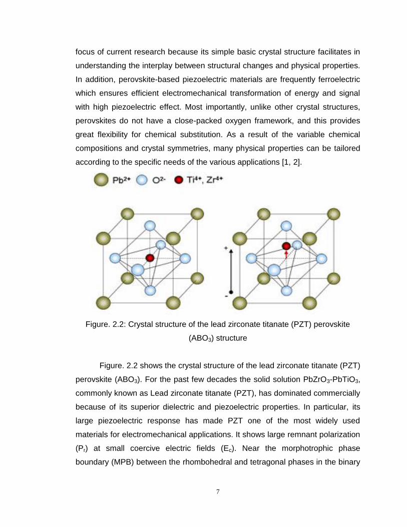


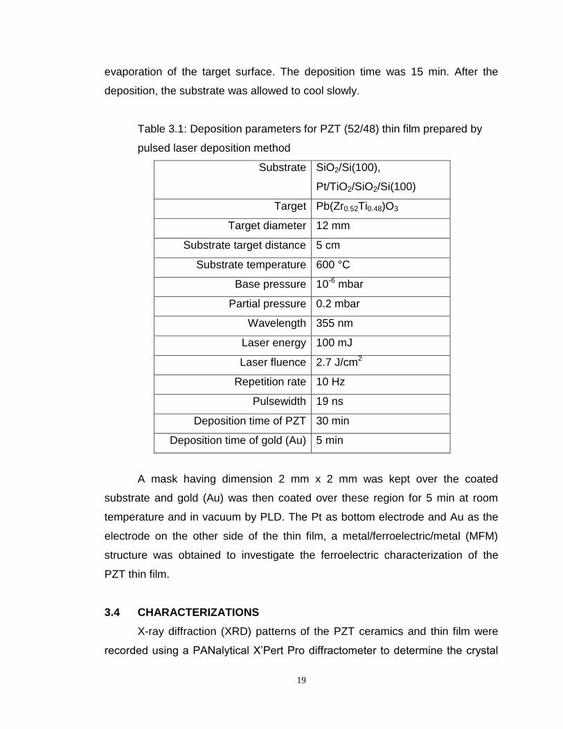


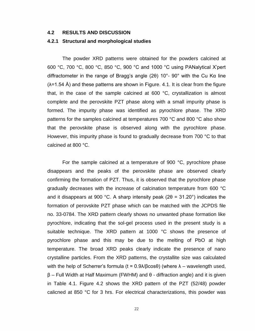
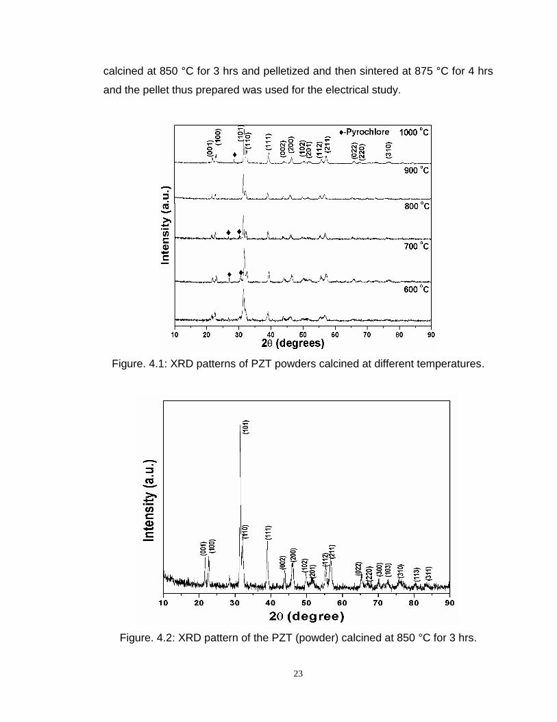
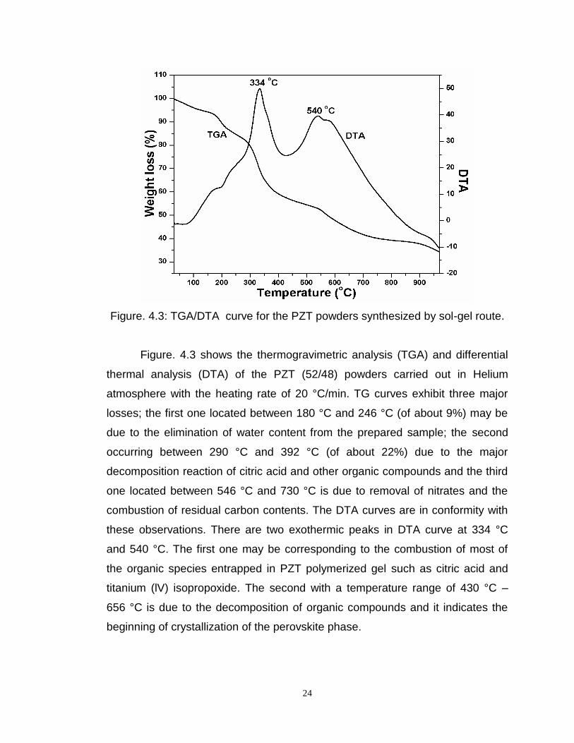
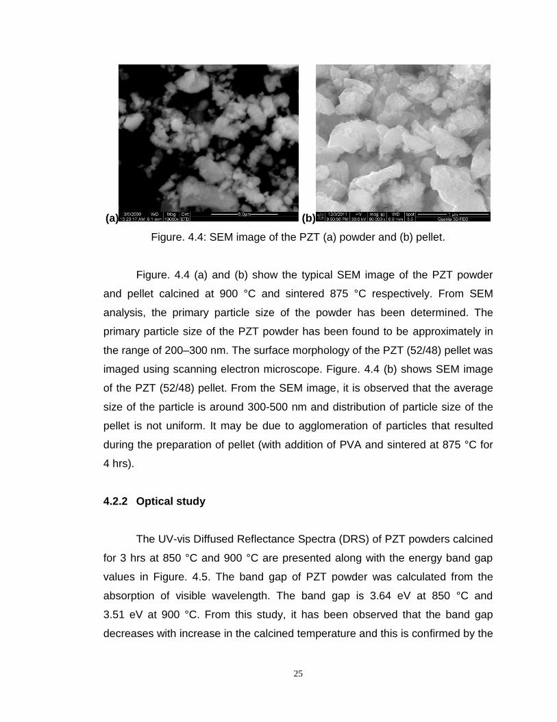


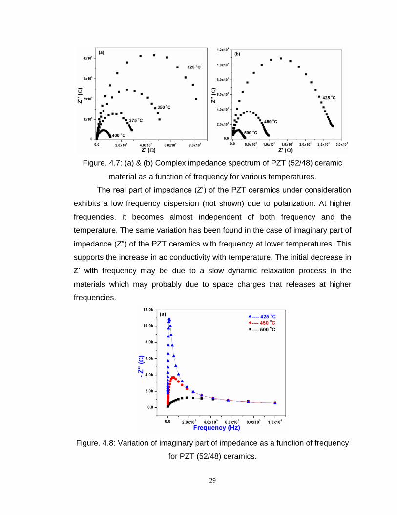


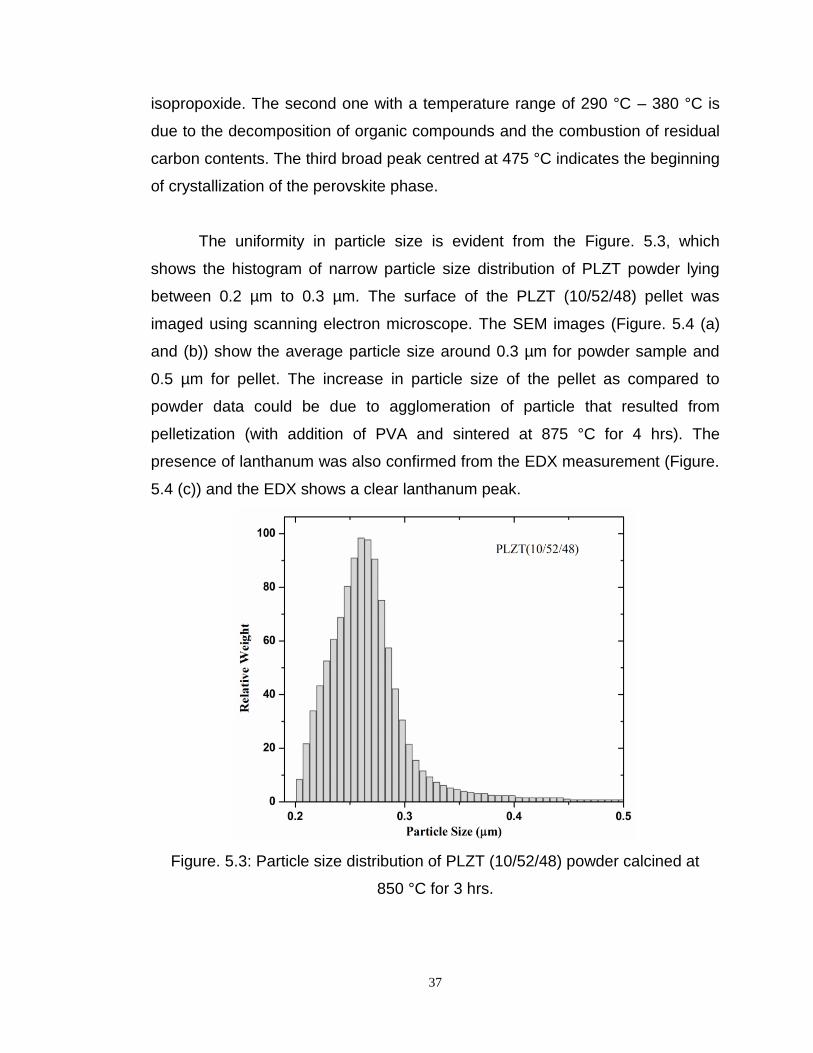
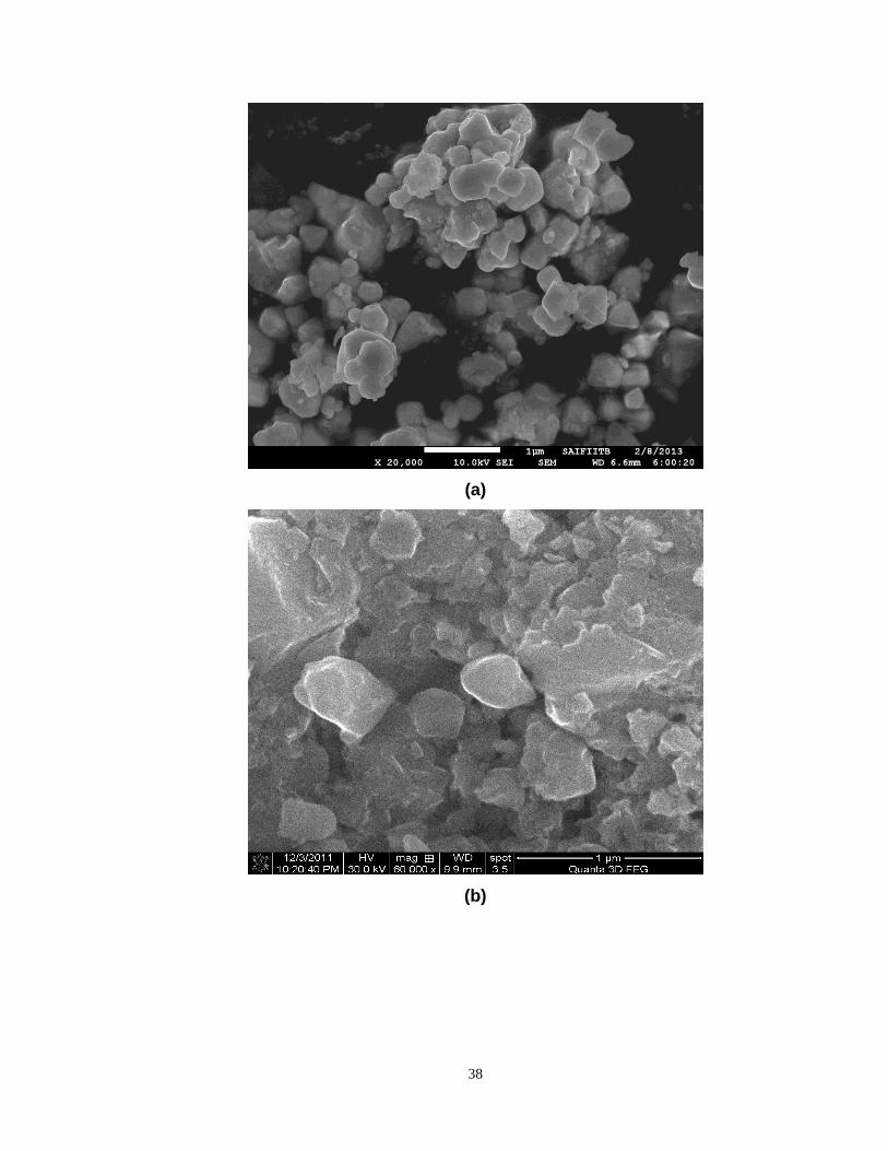

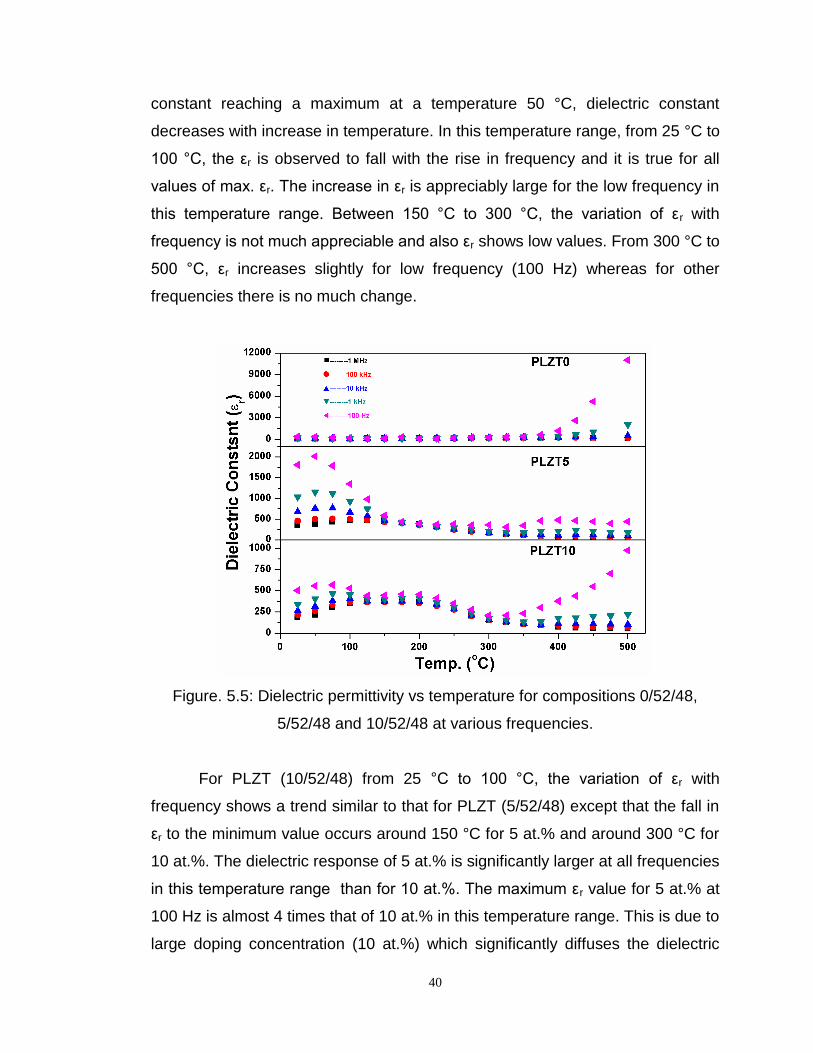


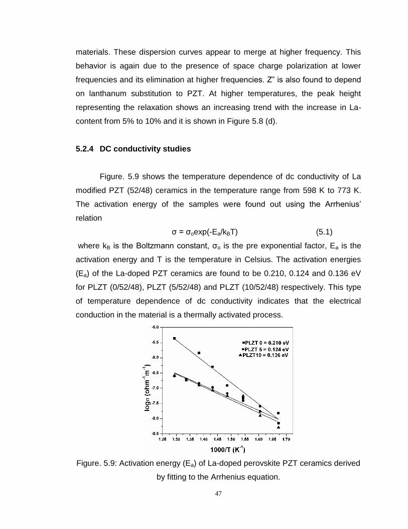


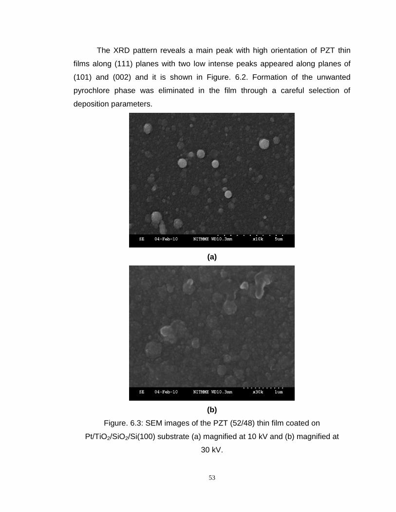

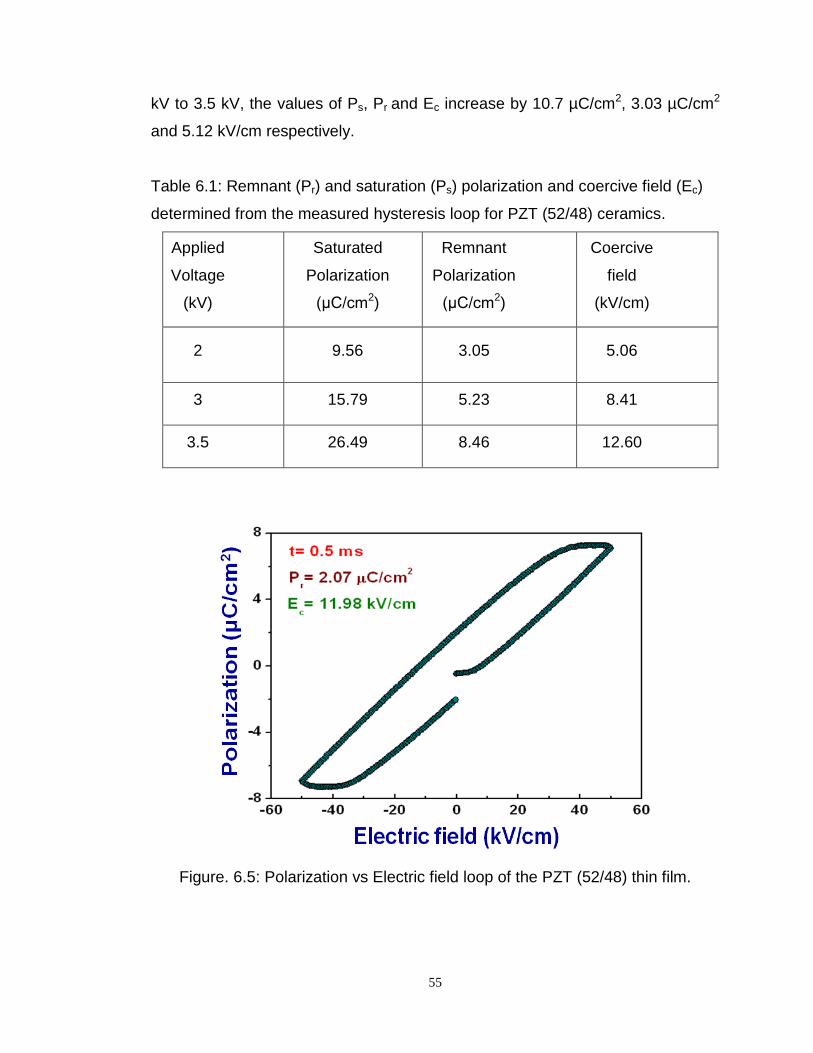


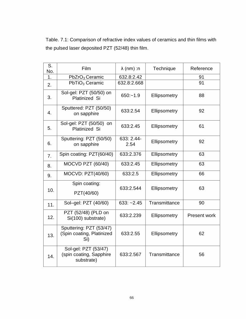
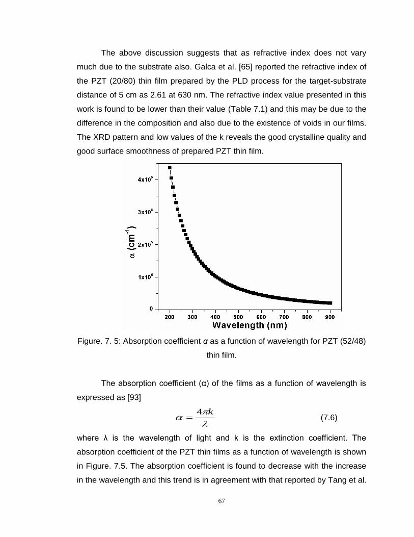


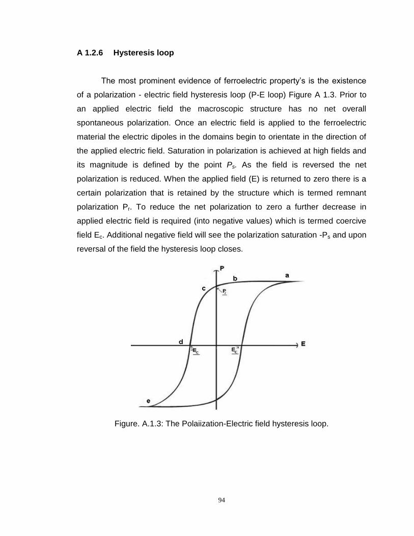


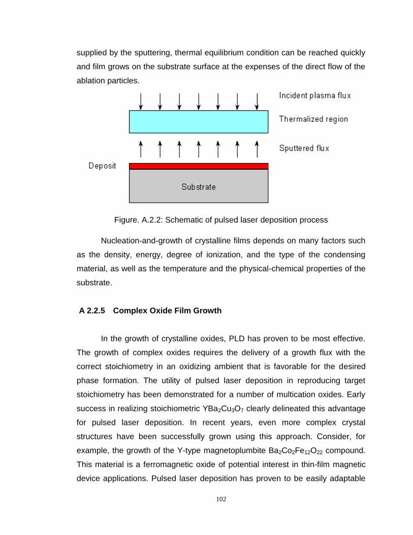


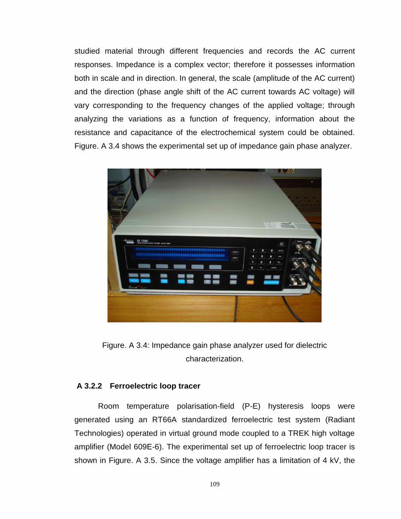


![Materials Chemistry and Physics · 2020. 3. 5. · ferent natural or synthetic piezoelectric ceramics (e.g. calcium titanate, barium titanate and lead zirconate titanate (PZT)) [2]](https://static.documents.pub/doc/80x56/60b88a1c38582264692512fa/materials-chemistry-and-physics-2020-3-5-ferent-natural-or-synthetic-piezoelectric.jpg)
