energies Article Studies on a Hybrid Full-Bridge/Half-Bridge Bidirectional CLTC Multi-Resonant DC-DC Converter with a Digital Synchronous Rectification Strategy Shu-huai Zhang 1 , Yi-feng Wang 1, * ID , Bo Chen 1 , Fu-qiang Han 1 and Qing-cui Wang 2 1 Key Laboratory of Smart Grid of Ministry of Education, Tianjin University, Tianjin 300072, China; [email protected] (S.-h.Z.); [email protected] (B.C.); [email protected] (F.-q.H.) 2 Tianjin Research Institute of Electric Science Co., Ltd. (TRIED), Tianjin 300300, China; [email protected]* Correspondence: [email protected]; Tel.: +86-185-2206-2559 Received: 18 December 2017; Accepted: 15 January 2018; Published: 18 January 2018 Abstract: This study presents a new bidirectional multi-resonant DC-DC converter, which is named CLTC. The converter adds an auxiliary transformer and an extra resonant capacitor based on a LLC resonant DC-DC converter, achieving zero-voltage switching (ZVS) for the input inverting switches and zero-current switching (ZCS) for the output rectifiers in all load range. The converter also has a wide gain range in two directions. When the load is light, a half-bridge configuration is adopted instead of a full-bridge configuration to solve the problem of voltage regulation. By this method, the voltage gain becomes monotonous and controllable. Besides, the digital synchronous rectification strategy is proposed in forward mode without adding any auxiliary circuit. The conduction time of synchronous rectifiers equals the estimation value of body diodes’ conduction time with the lightest load. Power loss analysis is also conducted in different situations. Finally, the theoretical analysis is validated by a 5 kW prototype. Keywords: bidirectional CLTC resonant DC-DC converter; light load; synchronous rectification strategy; power loss analysis 1. Introduction With advantage of ZVS + ZCS, the bidirectional resonant DC-DC converter (BRDC) is gaining more attention in DC distribution system or DC microgrid applications [1–8]. All the power switching devices, including metal oxide semiconductor field effect transistor (MOSFET) switches and diodes have the desirable soft-switching features, and the switching loss is greatly decreased. In addition, the electromagnetic interference (EMI) is also restricted. As a result, BRDCs are characterized by high efficiency, high power density and low EMI, and are applicable to high frequency applications [9,10]. Among all the BRDCs, the bidirectional series resonant converter (BSRC) is a candidate topology [11–16]. All the switches of a BSRC work in either ZVS or ZCS for a wide variation of voltage gains with phase-shift control [13]. A novel control scheme was developed for BSRC in discontinuous mode [14]. With the accumulation of energy packets to raise output voltage, it is possible to have a gain greater than one. A novel method for analyzing the frequency response is also presented based on a mixture of the Fourier and the average state-space methods [15]. The analysis method provides enough information to properly control the BSRC. A BSRC using a continuous current mode was proposed in [16]. Experimental results from a 6 kW prototype validated the theoretical analysis, and higher efficiency is obtained compared to the phase-shift DAB in a wide power range. However, the efficiency Energies 2018, 11, 227; doi:10.3390/en11010227 www.mdpi.com/journal/energies
Transcript
energies
Article
Studies on a Hybrid Full-Bridge/Half-BridgeBidirectional CLTC Multi-Resonant DC-DCConverter with a Digital SynchronousRectification Strategy
Shu-huai Zhang 1, Yi-feng Wang 1,* ID , Bo Chen 1, Fu-qiang Han 1 and Qing-cui Wang 2
Received: 18 December 2017; Accepted: 15 January 2018; Published: 18 January 2018
Abstract: This study presents a new bidirectional multi-resonant DC-DC converter, which is namedCLTC. The converter adds an auxiliary transformer and an extra resonant capacitor based on a LLCresonant DC-DC converter, achieving zero-voltage switching (ZVS) for the input inverting switchesand zero-current switching (ZCS) for the output rectifiers in all load range. The converter also hasa wide gain range in two directions. When the load is light, a half-bridge configuration is adoptedinstead of a full-bridge configuration to solve the problem of voltage regulation. By this method,the voltage gain becomes monotonous and controllable. Besides, the digital synchronous rectificationstrategy is proposed in forward mode without adding any auxiliary circuit. The conduction time ofsynchronous rectifiers equals the estimation value of body diodes’ conduction time with the lightestload. Power loss analysis is also conducted in different situations. Finally, the theoretical analysis isvalidated by a 5 kW prototype.
Keywords: bidirectional CLTC resonant DC-DC converter; light load; synchronous rectificationstrategy; power loss analysis
1. Introduction
With advantage of ZVS + ZCS, the bidirectional resonant DC-DC converter (BRDC) is gainingmore attention in DC distribution system or DC microgrid applications [1–8]. All the power switchingdevices, including metal oxide semiconductor field effect transistor (MOSFET) switches and diodeshave the desirable soft-switching features, and the switching loss is greatly decreased. In addition,the electromagnetic interference (EMI) is also restricted. As a result, BRDCs are characterized by highefficiency, high power density and low EMI, and are applicable to high frequency applications [9,10].Among all the BRDCs, the bidirectional series resonant converter (BSRC) is a candidate topology [11–16].All the switches of a BSRC work in either ZVS or ZCS for a wide variation of voltage gains withphase-shift control [13]. A novel control scheme was developed for BSRC in discontinuous mode [14].With the accumulation of energy packets to raise output voltage, it is possible to have a gain greaterthan one. A novel method for analyzing the frequency response is also presented based on a mixtureof the Fourier and the average state-space methods [15]. The analysis method provides enoughinformation to properly control the BSRC. A BSRC using a continuous current mode was proposedin [16]. Experimental results from a 6 kW prototype validated the theoretical analysis, and higherefficiency is obtained compared to the phase-shift DAB in a wide power range. However, the efficiency
is not ideal for the whole frequency range. A bidirectional LLC resonant DC-DC converter is also agood option. A bidirectional three-level LLC resonant converter has a very wide voltage gain rangewith PWAM control [17]. It overcomes the limitation of voltage gain in LLC resonant converters.A bidirectional LLC resonant converter with automatic forward and backward mode transition isproposed in [18]. An auxiliary inductor is added to raise the voltage gain in backward operation.Based on LLC, a symmetrical bidirectional CLLC resonant converter was recently proposed [19–21].The voltage gain in backward operation is the same as that in forward operation. However, with thegrowth of output power and voltage conversion ratio, the resonant inductance is small and the resonantcapacitance is big. These parameters are hard to design.
Besides, the regulation capability of a resonant DC-DC converter is weak under light loadconditions. Due to parasitic parameters in the resonant tank, the output voltage goes up asthe switching frequency increases, and an upturn drifting occurs in the voltage gain curve [22].This phenomenon causes trouble for voltage regulation under light load conditions. To solve thisproblem, many researchers have changed the control method for light load conditions [23–28]. Burstmode is used in [23,24], but the ripple of the output voltage is large and the dynamic response isslow. The phase-shift and PWM control methods are effective in [25–28], but the control scheme iscomplex due to the additional control elements. The changes are also conducted with the topologyof resonant DC-DC converter. Adding an additional output capacitor to switches can reduce currentripple and decrease powering transmitted between two sides of transformer [29], but the ZVS rangethis time is narrow. An additional capacitor is paralleled with the resonant inductor to improve thegain characteristics in [30]. ZVS is acquired under entire load condition, and efficiency is improvedwith less turn-off loss, but the design of the transformer and additional capacitor is complex due toresonance between leakage inductor and the additional capacitor.
The synchronous rectification (SR) strategy for resonant converters is also important towardachieving working efficiency [31–34]. A novel driving scheme with a compensation network forsynchronous rectifiers is used in LLC resonant converters. The conduction loss and switching lossare also reduced considerably [35]. A hybrid driving scheme for full-bridge SR is proposed in [36].It uses one transformer auxiliary winding to drive two high-side SR switches and a simple currenttransformer (CT) to drive two low-side SR switches. The proposed method operates well under DCMand CCM conditions. A novel SR control strategy is developed, through accurately tracking the targetswitching moments in [37]. However, the strategies above are complex in application and they arenot verified in BRDCs. A new synchronous rectification strategy, which is simpler and compatible tobidirectional power flow, needs to be developed.
In this study, a new bidirectional CLTC multi-resonant DC-DC converter is proposed. As Figure 1shows, the converter is composed of a high-voltage side (HVS) full-bridge, low-voltage side (LVS)full-bridge and a multi-resonant tank. An auxiliary transformer T2 and an extra resonant capacitorCr2 are added on bidirectional LLC resonant DC-DC converter, so the converter is named by CLTC.The gain range in two directions is broadened with the added devices. ZVS for the input invertingswitches and ZCS for the output rectifiers are realized in all load range. UH represents HVS DC voltage,while UL represents LVS DC voltage. Power flows in both forward and backward mode are modulatedwith pulse frequency modulation (PFM). In forward mode, S1 & S4 and S2 & S3 run with 50% dutycycle, the rectifier switches S6 & S7 and S5 & S8 are driven by the SR signals. In backward mode, S6 &S7 and S5 & S8 run at 50% duty cycle, S1 & S4 and S2 & S3 don’t work, diodes on HVS realize SR.
This paper is organized as follows: the operation principles and characteristic descriptions ofthe proposed converter are discussed in Section 2. Hybrid full-bridge/half-bridge configuration isused to improve the light load regulation capability in Section 3. Stresses of power devices, load andworking frequency range in half-bridge CLTC are also given to prove the feasibility of the half-bridgeconfiguration. SR strategy based on estimation of the diodes’ conduction time is proposed in Section 4.Power loss distribution and comparison tests are conducted with different loads and LVS DC voltagesin Section 5. A 5 kW prototype is built with HVS voltage of 400 V and LVS DC voltage of 42–58 V.
Energies 2018, 11, 227 3 of 22
Experimental results are shown to validate the theoretical analysis above in Section 6. Conclusions aredrawn in Section 7.
Energies 2018, 11, 227 2 of 22
efficiency is not ideal for the whole frequency range. A bidirectional LLC resonant DC-DC converter is also a good option. A bidirectional three-level LLC resonant converter has a very wide voltage gain range with PWAM control [17]. It overcomes the limitation of voltage gain in LLC resonant converters. A bidirectional LLC resonant converter with automatic forward and backward mode transition is proposed in [18]. An auxiliary inductor is added to raise the voltage gain in backward operation. Based on LLC, a symmetrical bidirectional CLLC resonant converter was recently proposed [19–21]. The voltage gain in backward operation is the same as that in forward operation. However, with the growth of output power and voltage conversion ratio, the resonant inductance is small and the resonant capacitance is big. These parameters are hard to design.
Besides, the regulation capability of a resonant DC-DC converter is weak under light load conditions. Due to parasitic parameters in the resonant tank, the output voltage goes up as the switching frequency increases, and an upturn drifting occurs in the voltage gain curve [22]. This phenomenon causes trouble for voltage regulation under light load conditions. To solve this problem, many researchers have changed the control method for light load conditions [23–28]. Burst mode is used in [23,24], but the ripple of the output voltage is large and the dynamic response is slow. The phase-shift and PWM control methods are effective in [25–28], but the control scheme is complex due to the additional control elements. The changes are also conducted with the topology of resonant DC-DC converter. Adding an additional output capacitor to switches can reduce current ripple and decrease powering transmitted between two sides of transformer [29], but the ZVS range this time is narrow. An additional capacitor is paralleled with the resonant inductor to improve the gain characteristics in [30]. ZVS is acquired under entire load condition, and efficiency is improved with less turn-off loss, but the design of the transformer and additional capacitor is complex due to resonance between leakage inductor and the additional capacitor.
The synchronous rectification (SR) strategy for resonant converters is also important toward achieving working efficiency [31–34]. A novel driving scheme with a compensation network for synchronous rectifiers is used in LLC resonant converters. The conduction loss and switching loss are also reduced considerably [35]. A hybrid driving scheme for full-bridge SR is proposed in [36]. It uses one transformer auxiliary winding to drive two high-side SR switches and a simple current transformer (CT) to drive two low-side SR switches. The proposed method operates well under DCM and CCM conditions. A novel SR control strategy is developed, through accurately tracking the target switching moments in [37]. However, the strategies above are complex in application and they are not verified in BRDCs. A new synchronous rectification strategy, which is simpler and compatible to bidirectional power flow, needs to be developed.
In this study, a new bidirectional CLTC multi-resonant DC-DC converter is proposed. As Figure 1 shows, the converter is composed of a high-voltage side (HVS) full-bridge, low-voltage side (LVS) full-bridge and a multi-resonant tank. An auxiliary transformer T2 and an extra resonant capacitor Cr2 are added on bidirectional LLC resonant DC-DC converter, so the converter is named by CLTC. The gain range in two directions is broadened with the added devices. ZVS for the input inverting switches and ZCS for the output rectifiers are realized in all load range. UH represents HVS DC voltage, while UL represents LVS DC voltage. Power flows in both forward and backward mode are modulated with pulse frequency modulation (PFM). In forward mode, S1 & S4 and S2 & S3 run with 50% duty cycle, the rectifier switches S6 & S7 and S5 & S8 are driven by the SR signals. In backward mode, S6 & S7 and S5 & S8 run at 50% duty cycle, S1 & S4 and S2 & S3 don’t work, diodes on HVS realize SR.
UH
ULCr1
S1 S3
S2 S4
S5 S7
S6 S8
CH CL
A
B
C
D
T1
T2
Lr
Cr2
*
*
Lm2 Lm1
n1:1
n2:1
Figure 1. The proposed bidirectional CLTC multi-resonant DC-DC converter. Figure 1. The proposed bidirectional CLTC multi-resonant DC-DC converter.
2. Operation Principles and Characteristic Description
In this section, the main operation principles of CLTC multi-resonant converter are given. It issimilar to a LLC resonant converter as two stages of resonance exist. The resonant frequency, voltagegain and ZVS characteristic are analyzed, forming research foundations for the following sections.
2.1. Operation Principles
Figure 2 shows different states of the CLTC multi-resonant converter. In Figure 2, iLm1 is excitationcurrent of transformer T1 on HVS, i’Lm1 is excitation current of transformer T1 on LVS, iLr is currentof resonant inductor, iCr1 and iCr2 are currents of resonant capacitors on HVS and LVS, uGS14 is thedriving signal of S1 and S4, uGS23 is the driving signal of S2 and S3, uGS58 is the driving signal of S5
and S8, uGS67 is the driving signal of S6 and S7, uDS14 is the drain-source voltage of S1 and S4, uDS23
is the drain-source voltage of S2 and S3, uDS58 is the drain-source voltage of S5 and S8, uDS67 is thedrain-source voltage of S6 and S7, iDS14 is the drain-source current of S1 and S4, iDS23 is the drain-sourcecurrent of S2 and S3, iDS58 is the drain-source current of S5 and S8, iDS67 is the drain-source current ofS6 and S7.
Energies 2018, 11, 227 3 of 22
This paper is organized as follows: the operation principles and characteristic descriptions of the proposed converter are discussed in Section 2. Hybrid full-bridge/half-bridge configuration is used to improve the light load regulation capability in Section 3. Stresses of power devices, load and working frequency range in half-bridge CLTC are also given to prove the feasibility of the half-bridge configuration. SR strategy based on estimation of the diodes’ conduction time is proposed in Section 4. Power loss distribution and comparison tests are conducted with different loads and LVS DC voltages in Section 5. A 5 kW prototype is built with HVS voltage of 400 V and LVS DC voltage of 42–58 V. Experimental results are shown to validate the theoretical analysis above in Section 6. Conclusions are drawn in Section 7.
2. Operation Principles and Characteristic Description
In this section, the main operation principles of CLTC multi-resonant converter are given. It is similar to a LLC resonant converter as two stages of resonance exist. The resonant frequency, voltage gain and ZVS characteristic are analyzed, forming research foundations for the following sections.
2.1. Operation Principles
Figure 2 shows different states of the CLTC multi-resonant converter. In Figure 2, iLm1 is excitation current of transformer T1 on HVS, i’Lm1 is excitation current of transformer T1 on LVS, iLr is current of resonant inductor, iCr1 and iCr2 are currents of resonant capacitors on HVS and LVS, uGS14 is the driving signal of S1 and S4, uGS23 is the driving signal of S2 and S3, uGS58 is the driving signal of S5 and S8, uGS67 is the driving signal of S6 and S7, uDS14 is the drain-source voltage of S1 and S4, uDS23 is the drain-source voltage of S2 and S3, uDS58 is the drain-source voltage of S5 and S8, uDS67 is the drain-source voltage of S6 and S7, iDS14 is the drain-source current of S1 and S4, iDS23 is the drain-source current of S2 and S3, iDS58 is the drain-source current of S5 and S8, iDS67 is the drain-source current of S6 and S7.
iDS14
S2&S3 S2&S3S1&S4
t0 t2 t3
uGS23
iLm1iLr
t1
uGS14
iDS23 iDS23
iDS67 iDS67
uDS14
uDS23
uDS14
S6&S7 S6&S7S5&S8
uGS67
uGS58
iDS58
uDS23 uDS14
iCr2
iDS58
iDS67
iDS14
iDS23
iLm1
iLr
S6&S7 S6&S7S5&S8
t0 t2 t3
uGS67
i'Lm1iCr2
t1
uGS58
uDS14
uDS23
uDS14
uDS67
uDS58
uDS23 uDS14
iCr1
iDS14
iDS23
uDS58 uDS67 uDS58
iDS14iDS23 iDS23
iDS67 iDS67iDS58iDS58
iDS67
i'Lm1
iCr2
(a) (b)
Figure 2. The current and voltage waveforms of CLTC multi-resonant converter: (a) forward mode; (b) backward mode.
2.1.1. Forward Mode
The equivalent circuits in forward mode are listed in Figure 3. Detailed descriptions and explanations of the operational modes in half period are as follows:
Mode A [t0–t1]: S2 and S3 have just turned off at t0. The HVS current charges the output capacitor of S2 and S3, and discharges the output capacitor of S1 and S4. After that, the HVS current passes through the antiparallel diode of S1 and S4, which makes the switches turn on under the ZVS condition.
Figure 2. The current and voltage waveforms of CLTC multi-resonant converter: (a) forward mode;(b) backward mode.
Energies 2018, 11, 227 4 of 22
2.1.1. Forward Mode
The equivalent circuits in forward mode are listed in Figure 3. Detailed descriptions andexplanations of the operational modes in half period are as follows:
Mode A [t0–t1]: S2 and S3 have just turned off at t0. The HVS current charges the output capacitorof S2 and S3, and discharges the output capacitor of S1 and S4. After that, the HVS current passesthrough the antiparallel diode of S1 and S4, which makes the switches turn on under the ZVS condition.Energies 2018, 11, 227 4 of 22
Cr1Cr2
S1 S3
S2 S4
S5 S7
S6 S8
A
B
C
D
*
*
UH ULCH CL
T1
T2
Lr
Lm2 Lm1
(a)
Cr1Cr2
S1 S3
S2 S4
S5 S7
S6 S8
A
B
C
D
*
*UH ULCH CL
T1
T2
Lr
Lm2 Lm1
(b)
Cr1Cr2
S1 S3
S2 S4
S5 S7
S6 S8
A
B
C
D
*
*
UH ULCH CL
T1
T2
Lr
Lm2 Lm1
(c)
Figure 3. Equivalent circuits for each stage in forward mode: (a) Mode A; (b) Mode B; (c) Mode C.
Mode B [t1–t2]: At t1, S1, S4, S5 and S8 turn on and power is transferred from HVS to LVS. The resonant current changes in a sine-wave with main resonant frequency, fr. At t2, iLr is equal to iLm1, iCr2 and ids58 become zero.
Mode C [t2–t3]: S1 and S4 are still on in this mode, S5 and S8 are off in this mode. As iCr2 and ids58 are zero in t2, S5 and S8 turn off under ZCS condition. The HVS goes into secondary resonance with the frequency of fr2f. At t3, S1 and S4 are off and ready to go into dead-time duration.
When working frequency is bigger than main resonant frequency, Mode C and ZCS of LVS power switches disappear like LLC. The turn-off currents increase largely in this situation.
2.1.2. Backward Mode
The equivalent circuits in backward mode are listed in Figure 4. L’m1 and L’m2 are the magnetizing inductors on LVS. The modes are similar to those in forward mode. Detail descriptions and explanations of the operational modes in half period are shown as follows:
Mode A [t0–t1]: S6 and S7 turn off at t0. The resonant current on LVS charges the output capacitor of S6 and S7, and discharges the output capacitor of S5 and S8. After that, the LVS current passes through the antiparallel diode of S5 and S8, which makes the switches turn on under the ZVS condition.
Mode B [t1–t2]: At t1, S5, S8, D1 and D4 turn on and power is transferred from LVS to HVS. The resonant current on LVS changes in a sine-wave with main resonant frequency. At t2, iCr2 is equal to i’Lm1, iCr1 and ids14 become zero.
Mode C [t2–t3]: S5 and S8 are still on in this mode, D1 and D4 are off in this mode. ZCS of D1 and D4 is realized as iCr1 and ids14 become zero at t2. The LVS goes into secondary resonance with the frequency of fr2b. At t3, S1 and S4 are off and ready to go into dead-time duration.
When working frequency is bigger than main resonant frequency, Mode C and ZCS of HVS diodes disappear like LLC. The turn-off currents increase largely in this situation.
Figure 3. Equivalent circuits for each stage in forward mode: (a) Mode A; (b) Mode B; (c) Mode C.
Mode B [t1–t2]: At t1, S1, S4, S5 and S8 turn on and power is transferred from HVS to LVS.The resonant current changes in a sine-wave with main resonant frequency, f r. At t2, iLr is equal toiLm1, iCr2 and ids58 become zero.
Mode C [t2–t3]: S1 and S4 are still on in this mode, S5 and S8 are off in this mode. As iCr2 and ids58are zero in t2, S5 and S8 turn off under ZCS condition. The HVS goes into secondary resonance withthe frequency of f r2f. At t3, S1 and S4 are off and ready to go into dead-time duration.
When working frequency is bigger than main resonant frequency, Mode C and ZCS of LVS powerswitches disappear like LLC. The turn-off currents increase largely in this situation.
2.1.2. Backward Mode
The equivalent circuits in backward mode are listed in Figure 4. L’m1 and L’m2 are the magnetizinginductors on LVS. The modes are similar to those in forward mode. Detail descriptions andexplanations of the operational modes in half period are shown as follows:
Mode A [t0–t1]: S6 and S7 turn off at t0. The resonant current on LVS charges the output capacitorof S6 and S7, and discharges the output capacitor of S5 and S8. After that, the LVS current passesthrough the antiparallel diode of S5 and S8, which makes the switches turn on under the ZVS condition.
Mode B [t1–t2]: At t1, S5, S8, D1 and D4 turn on and power is transferred from LVS to HVS.The resonant current on LVS changes in a sine-wave with main resonant frequency. At t2, iCr2 is equalto i’Lm1, iCr1 and ids14 become zero.
Energies 2018, 11, 227 5 of 22
Mode C [t2–t3]: S5 and S8 are still on in this mode, D1 and D4 are off in this mode. ZCS of D1
and D4 is realized as iCr1 and ids14 become zero at t2. The LVS goes into secondary resonance with thefrequency of f r2b. At t3, S1 and S4 are off and ready to go into dead-time duration.
When working frequency is bigger than main resonant frequency, Mode C and ZCS of HVS diodesdisappear like LLC. The turn-off currents increase largely in this situation.Energies 2018, 11, 227 5 of 22
T1
LrCr1
Cr2
D1 D3
D2 D4
S5 S7
S6 S8
A
B
C
D
T2*
*
UH ULCH CLL'm2
L'm1
(a)
T1
LrCr1
Cr2
S5 S7
S6 S8
A
B
C
D
T2
*
*
UH ULCH CLL'm2
L'm1
D1 D3
D2 D4
(b)
T1
LrCr1
Cr2
S5 S7
S6 S8
A
B
C
D
T2
*
*
UH ULCH CLL'm2
L'm1
D1 D3
D2 D4
(c)
Figure 4. Equivalent circuits for each stage in backward mode: (a) Mode A; (b) Mode B; (c) Mode C.
2.2. Characteristic Description
Main resonant frequency of CLTC converter in two power flows, fr, is:
r1
2AfB
(1)
where:
21 1 2A A A A (2)
2 2 2 2r1 m2 m1 r 1 2 m1 r r2 m2 1 m2 r r2 m1 2 r2 m1 m2 1 21 2C L L L n n L L C L n L L C L n C L L n nA (3)
2 42 r1 r2 m1 m2 r m1 m2 r 1 24A C C L L L L L L n n (4)
2r1 r2 m1 m2 r 22C C L L L nB (5)
fr is obtained when no load is added and imaginary part of AC input impedance of CLTC is zero. The secondary resonant frequency in forward mode, fr2f, and the secondary resonant frequency
in backward mode, fr2b, are:
r m1 m2
r2fr1 m2 r m1
12
L L Lf
C L L L
(6)
r2bm1 m2 r2
1
2f
L L C
(7)
fr2f and fr2b are obtained with the resonant capacitance and inductance in secondary resonance. The resonant capacitance and inductance are shown in Figures 3c and 4c.
Figure 4. Equivalent circuits for each stage in backward mode: (a) Mode A; (b) Mode B; (c) Mode C.
2.2. Characteristic Description
Main resonant frequency of CLTC converter in two power flows, f r, is:
fr =1
2π
√AB
(1)
where:A = A1 + A1
2 − A2 (2)
A1 = Cr1Lm2(Lm1 + Lr)n12n2
2 + (Lm1 + Lr)Cr2Lm2n12 + (Lm2 + Lr)Cr2Lm1n2
2 + 2Cr2Lm1Lm2n1n2 (3)
A2 = 4Cr1Cr2Lm1Lm2Lr(Lm1 + Lm2 + Lr)n12n2
4 (4)
B = 2Cr1Cr2Lm1Lm2Lrn22 (5)
f r is obtained when no load is added and imaginary part of AC input impedance of CLTC is zero.The secondary resonant frequency in forward mode, f r2f, and the secondary resonant frequency
in backward mode, f r2b, are:
fr2f =1
2π
√Lr + Lm1 + Lm2
Cr1Lm2(Lr + Lm1)(6)
fr2b =1
2π√(L′m1 + L′m2)Cr2
(7)
Energies 2018, 11, 227 6 of 22
f r2f and f r2b are obtained with the resonant capacitance and inductance in secondary resonance.The resonant capacitance and inductance are shown in Figures 3c and 4c.
By use of the fundamental harmonic analysis (FHA) method, Figures 5a and 6a show 3D voltagegain curves according to load Po and normalized working frequency f s/f r. GF is gain in forward modeand GB is gain in backward mode. As is shown in Figures 5b and 6b, when the working frequency isbelow the main resonant frequency, GF and GB increase at first and decrease subsequently with thegrowth of working frequency. The peak gains are more than 1 over all the load range and obtainedaround secondary resonant frequency, f r2f and f r2b. At main resonant frequency f r, the gain of theconverter is 1. As is shown in Figures 5c and 6c, when working frequency is above main resonantfrequency, GF and GB decrease with the growth of working frequency. When load is lighter, the voltagegain is higher and the slope of gain curve is sharper. Voltage gain range of CTLC converter is wideenough to adapt applications like battery charger and DC microgrid.
Energies 2018, 11, 227 6 of 22
By use of the fundamental harmonic analysis (FHA) method, Figures 5a and 6a show 3D voltage gain curves according to load Po and normalized working frequency fs/fr. GF is gain in forward mode and GB is gain in backward mode. As is shown in Figures 5b and 6b, when the working frequency is below the main resonant frequency, GF and GB increase at first and decrease subsequently with the growth of working frequency. The peak gains are more than 1 over all the load range and obtained around secondary resonant frequency, fr2f and fr2b. At main resonant frequency fr, the gain of the converter is 1. As is shown in Figures 5c and 6c, when working frequency is above main resonant frequency, GF and GB decrease with the growth of working frequency. When load is lighter, the voltage gain is higher and the slope of gain curve is sharper. Voltage gain range of CTLC converter is wide enough to adapt applications like battery charger and DC microgrid.
00.5
11.5
2 12
34
50
2
4
6
8
10
Po (kW)fs/fr
GF
0 0.2 0.4 0.6 0.8 1 12
34
50
2
4
6
8
10
Po (kW)fs/fr
GF
(a) (b)
1 1.2 1.4 1.6 1.8 2 12
34
50.7
0.8
0.9
1
1.1
Po (kW)fs/fr
GF
(c)
Figure 5. Voltage gain obtained by FHA model in forward mode: (a) whole frequency range; (b) fs < fr; (c) fs ≥ fr.
00.5
11.5
2 12
34
50
2
4
6
8
10
Po (kW)fs/fr
GB
0 0.2 0.4 0.6 0.8 1 12
34
50
2
4
6
8
10
Po (kW)fs/fr
GB
(a) (b)
Figure 5. Voltage gain obtained by FHA model in forward mode: (a) whole frequency range; (b) f s < f r;(c) f s ≥ f r.
Energies 2018, 11, 227 6 of 22
By use of the fundamental harmonic analysis (FHA) method, Figures 5a and 6a show 3D voltage gain curves according to load Po and normalized working frequency fs/fr. GF is gain in forward mode and GB is gain in backward mode. As is shown in Figures 5b and 6b, when the working frequency is below the main resonant frequency, GF and GB increase at first and decrease subsequently with the growth of working frequency. The peak gains are more than 1 over all the load range and obtained around secondary resonant frequency, fr2f and fr2b. At main resonant frequency fr, the gain of the converter is 1. As is shown in Figures 5c and 6c, when working frequency is above main resonant frequency, GF and GB decrease with the growth of working frequency. When load is lighter, the voltage gain is higher and the slope of gain curve is sharper. Voltage gain range of CTLC converter is wide enough to adapt applications like battery charger and DC microgrid.
00.5
11.5
2 12
34
50
2
4
6
8
10
Po (kW)fs/fr
GF
0 0.2 0.4 0.6 0.8 1 12
34
50
2
4
6
8
10
Po (kW)fs/fr
GF
(a) (b)
1 1.2 1.4 1.6 1.8 2 12
34
50.7
0.8
0.9
1
1.1
Po (kW)fs/fr
GF
(c)
Figure 5. Voltage gain obtained by FHA model in forward mode: (a) whole frequency range; (b) fs < fr; (c) fs ≥ fr.
00.5
11.5
2 12
34
50
2
4
6
8
10
Po (kW)fs/fr
GB
0 0.2 0.4 0.6 0.8 1 12
34
50
2
4
6
8
10
Po (kW)fs/fr
GB
(a) (b)
Figure 6. Cont.
Energies 2018, 11, 227 7 of 22Energies 2018, 11, 227 7 of 22
1 1.2 1.4 1.6 1.8 2 12
34
50.7
0.8
0.9
1
1.1
Po (kW)fs/fr
GB
(c)
Figure 6. Voltage gain obtained by FHA model in backward mode: (a) whole frequency range; (b) fs < fr; (c) fs ≥ fr.
In order to realize ZVS for HVS switches, in forward mode, the dead-time duration tdt_F should satisfy (6) using the ZVS mechanism analyzed by [19]. Coss_H is the output capacitance of HVS switch:
oss_H m2 r m1 s
dt_Fr m1 m2
16 ( )C L L L ft
L L L (8)
Similarly, in backward mode, the dead-time duration tdt_B of LVS switches should satisfy:
dt_B oss_L m1 m2 s16 ( )t C L L f (9)
Coss_L is the output capacitance of LVS switch in (7). The inequations can be easily satisfied with different loads and working frequencies, which is
good for efficiency. The tdt_F and tdt_B are set to 200 ns in experiments.
3. Hybrid Full-Bridge/Half-Bridge Configuration
In this section, the reason for the upturn phenomenon is analyzed. A full-bridge configuration is used with a normal load. Half-bridge configurations are used for light load conditions with the advantage of monotonous gain curve and lower frequency. Because the situations in forward and backward mode are similar, the discussion in this section is conducted only in forward mode, and details are not provided for the backward mode.
3.1. Half-Bridge Configuration at Light Load Condition
Using the analysis method proposed in [22], it is found that transformer wiring capacitance is the main factor leading to the upturn problem. As is shown in Figure 7a, the ideal gain curve without considering parasitic parameters in forward mode is monotonous with working frequency under light load conditions. However, the voltage gain curve considering transformer wiring capacitance and experimental gain curve has upturns. As the experiment gain curve is not monotonous, the gain cannot be regulated well with PFM. For example, the voltage gain of 1.02 in Figure 7a is obtained with four different working frequencies. When PFM is adopted to control LVS voltage, the working frequency may be around 1.4fr instead of 0.8fr, and fluctuates quickly as the gain curve is not monotonous.
To overcome the above problem, a half-bridge configuration is introduced in this paper to regulate the required output voltage. In forward mode, the full-bridge in HVS is transformed into a half-bridge by turning off Q3 and turning on Q4 incessantly. The voltage gain is reduced by half, with the same load and resonant parameters. Thus, when the voltage gain needed is below 1 under light load conditions, a half-bridge configuration is adopted and the required gain is obtained with lower working frequency. In Figure 7b, when the working frequency is around 0.35fr, twice the required gain is acquired in full-bridge configuration. Thus, a gain of 1.02 is acquired in half-bridge configuration with the same working frequency and load. Also, the gain of 1.02 is controllable in half-
Figure 6. Voltage gain obtained by FHA model in backward mode: (a) whole frequency range;(b) f s < f r; (c) f s ≥ f r.
In order to realize ZVS for HVS switches, in forward mode, the dead-time duration tdt_F shouldsatisfy (6) using the ZVS mechanism analyzed by [19]. Coss_H is the output capacitance of HVS switch:
tdt_F ≥16Coss_HLm2(Lr + Lm1) fs
Lr + Lm1 + Lm2(8)
Similarly, in backward mode, the dead-time duration tdt_B of LVS switches should satisfy:
tdt_B ≥ 16Coss_L(L′m1 + L′m2) fs (9)
Coss_L is the output capacitance of LVS switch in (7).The inequations can be easily satisfied with different loads and working frequencies, which is
good for efficiency. The tdt_F and tdt_B are set to 200 ns in experiments.
3. Hybrid Full-Bridge/Half-Bridge Configuration
In this section, the reason for the upturn phenomenon is analyzed. A full-bridge configurationis used with a normal load. Half-bridge configurations are used for light load conditions with theadvantage of monotonous gain curve and lower frequency. Because the situations in forward andbackward mode are similar, the discussion in this section is conducted only in forward mode, anddetails are not provided for the backward mode.
3.1. Half-Bridge Configuration at Light Load Condition
Using the analysis method proposed in [22], it is found that transformer wiring capacitanceis the main factor leading to the upturn problem. As is shown in Figure 7a, the ideal gain curvewithout considering parasitic parameters in forward mode is monotonous with working frequencyunder light load conditions. However, the voltage gain curve considering transformer wiringcapacitance and experimental gain curve has upturns. As the experiment gain curve is not monotonous,the gain cannot be regulated well with PFM. For example, the voltage gain of 1.02 in Figure 7a isobtained with four different working frequencies. When PFM is adopted to control LVS voltage,the working frequency may be around 1.4f r instead of 0.8f r, and fluctuates quickly as the gain curve isnot monotonous.
To overcome the above problem, a half-bridge configuration is introduced in this paper to regulatethe required output voltage. In forward mode, the full-bridge in HVS is transformed into a half-bridgeby turning off Q3 and turning on Q4 incessantly. The voltage gain is reduced by half, with the same loadand resonant parameters. Thus, when the voltage gain needed is below 1 under light load conditions,a half-bridge configuration is adopted and the required gain is obtained with lower working frequency.
Energies 2018, 11, 227 8 of 22
In Figure 7b, when the working frequency is around 0.35f r, twice the required gain is acquired infull-bridge configuration. Thus, a gain of 1.02 is acquired in half-bridge configuration with the sameworking frequency and load. Also, the gain of 1.02 is controllable in half-bridge mode, because theworking frequency decreases largely, away from the region where the gain is not monotonous.
Energies 2018, 11, 227 8 of 22
bridge mode, because the working frequency decreases largely, away from the region where the gain is not monotonous.
GF 1.02
fs/fr0.6 0.8 1 1.2 1.4 1.6
0.9
0.95
1
1.05
1.1
1.15
Ideal gain
Gain considering transformer wiring capacitance
Experimental gain
Required gain
(a)
GF 2.04
0.3 0.4 0.5 0.61
1.5
2
2.5
3
3.5
fs/fr
Ideal gain
Gain considering transformer wiring capacitance
Experimental gain
Twice of required gain
(b)
Figure 7. Voltage gain curve of full-bridge CLTC converter at light load condition. (a) Around gain of 1.02; (b) around again of 2.04.
0
Full-bridge with its maximum loadHalf-bridge with its minimum loadHalf-bridge with its maximum load
Volta
ge G
ain,
GF
fs
1.05Gr
Gr
fr
Full-bridge with its minimum load
fH,1,maxfH,1,min
Range of working frequency in half bridge mode
The trend of gain curve when the load gets lighter
Figure 8. Voltage gain curve of CLTC converter at light load condition.
Figure 7. Voltage gain curve of full-bridge CLTC converter at light load condition. (a) Around gain of1.02; (b) around again of 2.04.
Energies 2018, 11, 227 8 of 22
bridge mode, because the working frequency decreases largely, away from the region where the gain is not monotonous.
GF 1.02
fs/fr0.6 0.8 1 1.2 1.4 1.6
0.9
0.95
1
1.05
1.1
1.15
Ideal gain
Gain considering transformer wiring capacitance
Experimental gain
Required gain
(a)
GF 2.04
0.3 0.4 0.5 0.61
1.5
2
2.5
3
3.5
fs/fr
Ideal gain
Gain considering transformer wiring capacitance
Experimental gain
Twice of required gain
(b)
Figure 7. Voltage gain curve of full-bridge CLTC converter at light load condition. (a) Around gain of 1.02; (b) around again of 2.04.
0
Full-bridge with its maximum loadHalf-bridge with its minimum loadHalf-bridge with its maximum load
Volta
ge G
ain,
GF
fs
1.05Gr
Gr
fr
Full-bridge with its minimum load
fH,1,maxfH,1,min
Range of working frequency in half bridge mode
The trend of gain curve when the load gets lighter
Figure 8. Voltage gain curve of CLTC converter at light load condition. Figure 8. Voltage gain curve of CLTC converter at light load condition.
Energies 2018, 11, 227 9 of 22
The mechanism of transformation between full-bridge and half-bridge configuration is displayedin Figure 8. With the decrease of load in full-bridge configuration, the gain curve rises. Then,the full-bridge configuration is transformed into a half-bridge configuration, working frequency getslower and the gain curve is monotonous around Gr. At last, half-bridge configuration is used to adaptlighter load instead of full-bridge configuration. The mechanism of transforming full-bridge intohalf-bridge is simple and effective, still, several considerations of the method are discussed here.
3.2. Voltage and Current Stresses
The stresses in both full-bridge and half-bridge configurations need to be checked. Voltage stressesof all the switches do not change. When the same power is transmitted, current stresses of LVS switchesstay the same. Current stresses of HVS switches in half-bridge are twice of those in full-bridge as theAC input voltage is cut by half. Thus, the load must be light if half-bridge is adopted, to ensure thecurrent amplitude is acceptable.
3.3. Load and Working Frquency Range
The peak gain should be larger than the required gain, Gr. It is because if the peak gain is smallerthan Gr, Gr cannot be tracked. Taking a margin of 0.05Gr into consideration, the DC output resistancein half-bridge configuration, Ro,H, should satisfy the following equation:
GF,H( fH,1, Ro,H) ≥ 1.05Gr (10)
In (8), GF,H is the voltage gain of half-bridge CLTC, f H,1 is the maximum point.Also, Ro,H should be bigger than twice of the rated resistance, Ro,H,rated, in full-bridge.
As Section 3.2 tells, the selection of Ro,H should guarantee that the current stresses in half-bridgeare no bigger than those in full-bridge. Thus:
Ro,H ≥ 2Ro,F,rated (11)
The working frequency of CLTC in half-bridge configuration, should be in the range of [f H,1,max,f r]. The working frequency should be lower than f r to avoid upturn phenomenon of gain curve.Also, when load is heavier in half-bridge, f H,1 gets larger as Figure 8 shows, so the lower limit of theworking frequency is the largest value of f H,1, f H,1,max. In the range of [f H,1,max, f r], the gain curvemonotonously declines with working frequency, and the slope is sharper in half-bridge configuration.It is ideal for voltage regulation of CLTC.
4. Synchronous Rectification Strategy Based on Estimation of Body Diodes’ Conduction Time
In consideration of improving the efficiency, a digital synchronous rectification strategy isproposed in forward mode. No auxiliary circuit is added. The proposed strategy adjusts conductiontime of switches in LVS by calculating rectifier diodes’ conduction time in half period, tSR. A wholeprocess of calculating tSR is proposed and verified in this section. It can be used in both full-bridgeconfiguration and half-bridge configuration.
4.1. Synchornous Rectification Strategy
With the proposed digital synchronous rectification strategy, all the driving signals of HVSswitches S1–S4 and LVS SR switches S5–S8 are given by STM32F series chip. The turn-on time of SRswitches is set to the same with HVS main switches. But the conduction time (the interval betweenturn-on and turn-off time) is set with the estimation value of body diodes’ conduction time in halfperiod, tSR, so tSR should be calculated for synchronous rectification.
Energies 2018, 11, 227 10 of 22
4.2. Estimation of the Body Diodes’ Conduction Time
When working frequency of CLTC is larger than main resonant frequency, tSR is half workingperiod because the secondary resonance doesn’t exist. However, when working frequency is smallerthan main resonant frequency, tSR is a variable with respect to Ro and f s. So discussion is focused ontSR when working frequency is smaller than main resonant frequency.
Energies 2018, 11, 227 10 of 22
4.2. Estimation of the Body Diodes’ Conduction Time
When working frequency of CLTC is larger than main resonant frequency, tSR is half working period because the secondary resonance doesn’t exist. However, when working frequency is smaller than main resonant frequency, tSR is a variable with respect to Ro and fs. So discussion is focused on tSR when working frequency is smaller than main resonant frequency.
ULT1
T2
Lr
Cr1 Cr2
D5 D7
D6 D8
CL
A
B
C
D
**
uAB
+
-
+
-
iLm2 iLm1 iCr2
Ro
Io
+-uCr2
iCr1
+ -uCr1
iLr
+
-uLm2 uLm1
+
-
n1:1
n2:1
Lm2 Lm1
Figure 9. Topology decomposition in forward mode without synchronous rectification strategy.
In Figure 9, assuming resonant current on LVS, iCr2, is approximated to a sinusoidal pulse:
Cr2 SRSRCr2
SR
sin( ), 0
0,
tI t tti
t t T (12)
ICr2 is the peak value of iCr2, t is the real time, T2 is half period, 1/(2fs). The value of uAB is UH in this period.
By using the law of conservation of electric charge, it can be obtained that:
SR
Cr2 o 20SR
sin( )
t tI dt I Tt
(13)
According to (13), ICr2 can be expressed by:
2
Cr2 oSR2T
I It
(14)
The voltage of Cr2 can be expressed by:
Cr2 Cr2 Cr2 00r2 SR
1( ) sin( ) ,
t tu t I dt UC t
(15)
As iCr2 is 0 and the voltage of Cr2 stays the same during tSR–T2, the following equation is found:
Cr2,0 Cr2 2 Cr2 SR( ) ( )U u T u t (16)
Applying (15) into (16), the UCr2,0 can be expressed by:
2
SR LCr2,0
r2 2 o2t U
UC T R
(17)
The voltage of magnetizing inductance Lm1 and Lm2, uLm1 and uLm2, can form following equations:
Lm1 Lm2L Cr2
1 2
Cr2rLm1 r Lm2
m1 1
( ) ( )( )
( )1(1 ) ( ) ( )
u t u tU U t
n ndi tL
u t L u tL n dt
(18)
so uLm2 can be expressed by:
Figure 9. Topology decomposition in forward mode without synchronous rectification strategy.
In Figure 9, assuming resonant current on LVS, iCr2, is approximated to a sinusoidal pulse:
iCr2 =
ICr2 sin(π×t
tSR), 0 ≤ t ≤ tSR
0, tSR ≤ t ≤ T(12)
ICr2 is the peak value of iCr2, t is the real time, T2 is half period, 1/(2f s). The value of uAB is UH inthis period.
By using the law of conservation of electric charge, it can be obtained that:
∫ tSR
0ICr2 sin(
π × ttSR
) dt = Io × T2 (13)
According to (13), ICr2 can be expressed by:
ICr2 = IoπT2
2tSR(14)
The voltage of Cr2 can be expressed by:
uCr2(t) =1
Cr2
∫ t
0ICr2 sin(
π × ttSR
) dt + UCr2,0 (15)
As iCr2 is 0 and the voltage of Cr2 stays the same during tSR–T2, the following equation is found:
UCr2,0 = −uCr2(T2) = −uCr2(tSR) (16)
Applying (15) into (16), the UCr2,0 can be expressed by:
UCr2,0 = − tSR2UL
2Cr2T2Ro(17)
The voltage of magnetizing inductance Lm1 and Lm2, uLm1 and uLm2, can form following equations: uLm1(t)n1
+ uLm2(t)n2
= UL + UCr2(t)
(1 + LrLm1
)uLm1(t) + 1n1
LrdiCr2(t)
dt = uLm2(t)(18)
Energies 2018, 11, 227 11 of 22
so uLm2 can be expressed by:
uLm2(t) =n2n1
LrdiCr2(t)
dt + (1 + LrLm1
)n1n2[UL + UCr2(t)]
n2 + n1(1 + LrLm1
)(19)
The instantaneous voltage between HVS full-bridge legs, uAB, can be expressed as:
uAB(t) = UCr1,0 +1
Cr1
∫ t
0iCr1(t) dt + uLm2(t) (20)
where, UCr1,0 is the initial voltage of resonant capacitor Cr1 at t0, and the instantaneous current of Cr1,iCr1, can be expressed as:
iCr1(t) = iLm1(t) + iLm2(t) + (1n1
+1n2
)iCr2(t) (21)
In order to simplify calculation process, Lm2 is supposed to be subject to uAB during 0–tSR. SoiLm2 and iLm1 can be expressed as linearly increasing currents:
iLm1(t) =UH
2(Lm1 + Lr)t + ILm1,0 (22)
iLm2(t) =UH
2Lm2t + ILm2,0 (23)
ILm1,0 and ILm2,0 is the initial value of ILm1 and ILm2:
ILm1,0 = − UH × tSR
4(Lm1 + Lr)(24)
ILm2,0 = −UH × tSR
4Lm2(25)
Realizing that uAB(t) = UH and substituting (19) and (21) into (20), gives:
UH = UCr1,0 +1
Cr1
∫ t0
[iLm1(t) + iLm2(t) + ( 1
n1+ 1
n2)iCr2(t)
]dt +
n2n1
LrdiCr2(t)
dt +(1+ LrLm1
)n1n2[UL+UCr2(t)]
n2+n1(1+Lr
Lm1)
(26)
Getting the derivative of the above equation:
0 = −Dπ2
tSR2 sin(
π × ttSR
) + E× sin(π × ttSR
) + F× tSR × t +ILm1,0 + ILm2,0
ICr2(27)
In (27), D, E, F are:
D =Cr1n2Lr
n1
[n2 + n1(1 + Lr
Lm1)] (28)
E =Cr1(1 + Lr
Lm1)n1n2
Cr2
[n2 + n1(1 + Lr
Lm1)] + 1
n1+
1n2
(29)
F =
[1
2(Lm1 + Lr)+
12Lm2
]UH
ICr2tSR(30)
UH can be expressed as UL/MSD, so F can be simplified by:
F =
[1
2(Lm1 + Lr)+
12Lm2
]2Ro
πT2MSD(31)
Energies 2018, 11, 227 12 of 22
ILm1,0+ILm2,0ICr2
is close to 0 as ICr2 is much larger than ILm1,0 + ILm2,0. When t is close to 0, π×ttSR≈
sin(
π×ttSR
), tSR is the solution of (27):
tSR =
√−πE + π
√E2 + 4DFπ
2F(32)
In Figure 10, the normalized estimated conduction time tSR/T2 versus normalized operatingfrequency f s/f r and different load (dots—simulation, solid lines—theoretical prediction). Figure 10reveals good agreement between theoretical values and simulation results. The curve of tSR/T2 isbasically proportional to f s/f r, and grows with the increase of load.
Based on the above analysis, the conduction time of LVS switches is set to estimated conductiontime tSR obtained when load is the lightest, so the conduction time of LVS switches in the proposedsynchronous rectification strategy is not relevant to the load. It is a parameter changing with operatingfrequency. LVS switches turn on firstly to reduce conduction loss. Then, as estimated conductiontime tSR is a little smaller than the real conduction time of LVS body diodes, the body diodes of LVSswitches conduct until the LVS resonant current becomes zero. Efficiency is not affected because theduration when body diodes conduct is short. The proposed digital synchronous rectification strategyis simple and effective, the effects are discussed in sections below.
Energies 2018, 11, 227 12 of 22
H
m1 r m2 Cr2 SR
1 12( ) 2
UF
L L L I t
(30)
UH can be expressed as UL/MSD, so F can be simplified by:
o
m1 r m2 2 SD
21 12( ) 2
RF
L L L T M
(31)
Lm1,0 Lm2,0
Cr2
I II
is close to 0 as ICr2 is much larger than ILm1,0 + ILm2,0. When t is close to 0,
SR SR
sin
t tt t
, tSR is the solution of (27):
2
SR4
2E E DFt
F
(32)
In Figure 10, the normalized estimated conduction time tSR/T2 versus normalized operating frequency fs/fr and different load (dots—simulation, solid lines—theoretical prediction). Figure 10 reveals good agreement between theoretical values and simulation results. The curve of tSR/T2 is basically proportional to fs/fr, and grows with the increase of load.
Based on the above analysis, the conduction time of LVS switches is set to estimated conduction time tSR obtained when load is the lightest, so the conduction time of LVS switches in the proposed synchronous rectification strategy is not relevant to the load. It is a parameter changing with operating frequency. LVS switches turn on firstly to reduce conduction loss. Then, as estimated conduction time tSR is a little smaller than the real conduction time of LVS body diodes, the body diodes of LVS switches conduct until the LVS resonant current becomes zero. Efficiency is not affected because the duration when body diodes conduct is short. The proposed digital synchronous rectification strategy is simple and effective, the effects are discussed in sections below.
0.4 0.5 0.6 0.7 0.8 0.9 10.4
0.6
0.8
1
fs/fr
tSR/T2
Simulation with full load
Simulation with half load
Estimation with full load
Estimation with half load
Conduction time with the lightest load used in the proposed synchronous rectification strategy
Figure 10. Normalized estimated conduction time tSR/T2 in calculation and simulation.
5. Power Loss Analysis
The power loss of converters is the key factor for component selection and design. In this section, the power loss distribution is calculated with mathematical models and compared with different LVS DC voltages. The HVS DC voltage of the converter stays the same. The power loss with half-bridge configuration and synchronous rectification strategy are discussed in this section, too.
Before further analysis, several parameters are defined as follows, PHSW,off is the turn-off loss of HVS power switches, PHSW,con is the conduction loss of HVS power switches, PLSW,off is the turn-off loss of LVS power switches, PLSW,con is the conduction loss of LVS power switches, PL is the power loss of
Figure 10. Normalized estimated conduction time tSR/T2 in calculation and simulation.
5. Power Loss Analysis
The power loss of converters is the key factor for component selection and design. In this section,the power loss distribution is calculated with mathematical models and compared with different LVSDC voltages. The HVS DC voltage of the converter stays the same. The power loss with half-bridgeconfiguration and synchronous rectification strategy are discussed in this section, too.
Before further analysis, several parameters are defined as follows, PHSW,off is the turn-off loss ofHVS power switches, PHSW,con is the conduction loss of HVS power switches, PLSW,off is the turn-offloss of LVS power switches, PLSW,con is the conduction loss of LVS power switches, PL is the powerloss of resonant inductor, PT,Σ is the total power loss of transformers, PWIRE,con is the conduction lossin printed circuit board and copper bar, PHD is the power loss of HVS diodes, PLD is the power loss ofLVS body diodes in power switches.
5.1. Loss Distribution with Different LVS DC Voltages
Power loss distribution with 5 kW load in forward and backward mode is shown in Figure 11.The power loss distribution is conducted with three LVS DC voltages of 42, 50 and 58 V and the HVS
Energies 2018, 11, 227 13 of 22
voltage of 400 V. In forward mode, the column of “50 V” is obtained around main resonant frequency,while the column of “42 V” is obtained with higher frequency and column of “58 V” is obtained withlower frequency. In backward mode, the column of “50 V” is obtained around main resonant frequency,while the column of “42 V” is obtained with lower frequency and column of “58 V” is obtained withhigher frequency.
Energies 2018, 11, 227 13 of 22
resonant inductor, PT,Σ is the total power loss of transformers, PWIRE,con is the conduction loss in printed circuit board and copper bar, PHD is the power loss of HVS diodes, PLD is the power loss of LVS body diodes in power switches.
5.1. Loss Distribution with Different LVS DC Voltages
Power loss distribution with 5 kW load in forward and backward mode is shown in Figure 11. The power loss distribution is conducted with three LVS DC voltages of 42, 50 and 58 V and the HVS voltage of 400 V. In forward mode, the column of “50 V” is obtained around main resonant frequency, while the column of “42 V” is obtained with higher frequency and column of “58 V” is obtained with lower frequency. In backward mode, the column of “50 V” is obtained around main resonant frequency, while the column of “42 V” is obtained with lower frequency and column of “58 V” is obtained with higher frequency.
400
350
300
250
200
150
100
50
0 42 V 50 V 58 V
PWIRE,con
PT,Σ
PHSW,off
PHSW,con
PL
PLSW,off
PLSW,con
PWIRE,con
PT,Σ
PHSW,offPHSW,con
PL
PLSW,con
PWIRE,con
PT,Σ
PHSW,off
PHSW,con
PL
PLSW,con
Loss comparison in forward mode with 5 kW load and different LVS DC voltages
Pow
er L
oss (
W)
(a)
400
350
300
250
200
150
100
50
0
PWIRE,con
PT,Σ
PHD
PL
PLSW,off
PLSW,con
PL
PLSW,con
PHD
PLSW,off
PT,Σ
PWIRE,con
PL
PLSW,con
PHD
PLSW,off
PT,Σ
PWIRE,con
Loss comparison in backward mode with 5 kW load and different LVS DC voltages
42 V 50 V 58 V
Pow
er L
oss (
W)
(b)
Figure 11. The power loss distribution with 5 kW and different LVS DC voltages: (a) forward mode; (b) backward mode.
Figure 11. The power loss distribution with 5 kW and different LVS DC voltages: (a) forward mode;(b) backward mode.
PHSW,off and PLSW,off are the dominant power losses. PL and PT,Σ change little with the change ofLVS DC voltage. PWIRE,con is large due to proximity effect and skin effect. The column of “42 V” inforward mode and the column of “58 V” in backward mode have greater power loss compared to the
Energies 2018, 11, 227 14 of 22
other columns. This is mainly because PHSW,off and PLSW,off are larger due to larger turn-off currentsand higher working frequencies. The HVS switches are SiC power devices, and the LVS switches are Sipower devices. Compared to LVS switches, the HVS switches have less turn-off delay time and falltime. So the switching loss of LVS switches is larger than that of HVS switches. Thus, the efficiency inforward mode is higher than that in backward mode in general.
5.2. Power Loss Distribution and Comparison between Full-Bridge and Half-Bridge Configuration
The power loss distribution and comparison between full-bridge and half-bridge configuration ismade to demonstrate the advantage of half-bridge configuration in efficiency. Taking forward mode forexample, changing from full-bridge configuration to half-bridge configuration has impacts as follows:
(1) PHSW,off and PLSW,off decrease largely. In forward mode, switches staying on on-off mode in HVSdecrease from 4 to 2, and their working frequency decreases from 160 kHz to around 40 kHz.So PHSW,off decreases largely with half-bridge configuration. Also, PLSW,off decreases with lessturn-off current and lower working frequency.
(2) The conduction loss of all devices increases. Resonant current on HVS increases to about twice,so PHSW,con, conduction loss of resonant inductor and primary windings of transformers areamplified. However, as resonant current on LVS changes little, PLSW,con and the conduction lossof secondary windings in transformers stay the same.
(3) Core loss of resonant inductor and transformers stays the same. In half-bridge LLC, workingfrequency f s decreases. However, Bmax, the peak flux density, increases because peak value ofcurrent increases. With Steinmetz’s equation Pcore = Kf s
αBmaxβVe, the core losses of resonant
inductor and transformers in half-bridge configuration change little.
Figure 12a shows power loss distribution and comparison with load of 200 W in forwardmode. Efficiencies of half-bridge and full-bridge configuration are 87.7% and 86.7%. The powerloss distribution is in accordance with the above analysis. Compared to full-bridge configuration,efficiency is a little higher in half-bridge configuration.
Figure 12b shows power loss distribution and comparison with load of 200 W in backward mode.PLSW,off gets much smaller in half-bridge configuration. The power loss is cut down by 26.7% and theefficiency is 81.5% in half-bridge configuration.
Energies 2018, 11, 227 14 of 22
PHSW,off and PLSW,off are the dominant power losses. PL and PT,Σ change little with the change of LVS DC voltage. PWIRE,con is large due to proximity effect and skin effect. The column of “42 V” in forward mode and the column of “58 V” in backward mode have greater power loss compared to the other columns. This is mainly because PHSW,off and PLSW,off are larger due to larger turn-off currents and higher working frequencies. The HVS switches are SiC power devices, and the LVS switches are Si power devices. Compared to LVS switches, the HVS switches have less turn-off delay time and fall time. So the switching loss of LVS switches is larger than that of HVS switches. Thus, the efficiency in forward mode is higher than that in backward mode in general.
5.2. Power Loss Distribution and Comparison between Full-Bridge and Half-Bridge Configuration
The power loss distribution and comparison between full-bridge and half-bridge configuration is made to demonstrate the advantage of half-bridge configuration in efficiency. Taking forward mode for example, changing from full-bridge configuration to half-bridge configuration has impacts as follows:
(1) PHSW,off and PLSW,off decrease largely. In forward mode, switches staying on on-off mode in HVS decrease from 4 to 2, and their working frequency decreases from 160 kHz to around 40 kHz. So PHSW,off decreases largely with half-bridge configuration. Also, PLSW,off decreases with less turn-off current and lower working frequency.
(2) The conduction loss of all devices increases. Resonant current on HVS increases to about twice, so PHSW,con, conduction loss of resonant inductor and primary windings of transformers are amplified. However, as resonant current on LVS changes little, PLSW,con and the conduction loss of secondary windings in transformers stay the same.
(3) Core loss of resonant inductor and transformers stays the same. In half-bridge LLC, working frequency fs decreases. However, Bmax, the peak flux density, increases because peak value of current increases. With Steinmetz’s equation Pcore = KfsαBmaxβVe, the core losses of resonant inductor and transformers in half-bridge configuration change little.
Figure 12a shows power loss distribution and comparison with load of 200 W in forward mode. Efficiencies of half-bridge and full-bridge configuration are 87.7% and 86.7%. The power loss distribution is in accordance with the above analysis. Compared to full-bridge configuration, efficiency is a little higher in half-bridge configuration.
Figure 12b shows power loss distribution and comparison with load of 200 W in backward mode. PLSW,off gets much smaller in half-bridge configuration. The power loss is cut down by 26.7% and the efficiency is 81.5% in half-bridge configuration.
35
30
25
20
15
10
5
0
Loss comparison between full-bridge and half-bridge mode with 200 W loadin forward mode
Half-bridge mode Full-bridge mode
PWIRE,con
PT,Σ
PHSW,off
PHSW,con
PL
PLSW,con
PWIRE,con
PT,Σ
PHSW,off
PHSW,con
PL
PLSW,con
PLSW,off
Pow
er L
oss (
W)
(a)
Figure 12. Cont.
Energies 2018, 11, 227 15 of 22Energies 2018, 11, 227 15 of 22
Loss comparison between full-bridge and half-bridge mode with 200 W loadin backward mode
70
60
50
40
30
20
10
0 Half-bridge mode Full-bridge mode
PWIRE,con
PT,Σ
PHD
PL
PLSW,con
PLSW,off
PWIRE,con
PT,Σ
PHD
PL
PLSW,con
PLSW,off
Pow
er L
oss (
W)
(b)
Figure 12. The power loss distribution and comparison between full-bridge and half-bridge configuration with 200 W load: (a) forward mode; (b) backward mode.
5.3. Power Loss Distribution and Comparison with and without Synchronous Strategy
Figure 13 shows the power loss distribution and comparison with and without synchronous strategy. When body diodes of LVS switches are used to realize rectification, PLD is quite large with diode forward voltage of 0.9 V. However, the drain-source on-state resistance of LVS switches is only 0.7 mΩ. Thus, with the use of the proposed synchronous strategy, PLSW,con is quite small. The total loss is cut by 49% with the use of synchronous strategy, showing the advantage in power loss reduction and efficiency enhancement.
400
350
300
250
200
150
100
50
0
PWIRE,con
PT,Σ
PHSW,off
PHSW,con
PL
PLSW,con
PWIRE,con
PT,Σ
PHSW,off
PHSW,con
PL
PLD
With synchronous strategy Without synchronous strategy
Loss comparison with and without synchronous strategy
Pow
er L
oss (
W)
Figure 13. The power loss distribution and comparison with and without synchronous strategy.
6. Experimental Results
A 5 kW prototype is built in the laboratory to verify the above analysis. The parameters of the components are listed in Table 1.
Figure 12. The power loss distribution and comparison between full-bridge and half-bridgeconfiguration with 200 W load: (a) forward mode; (b) backward mode.
5.3. Power Loss Distribution and Comparison with and without Synchronous Strategy
Figure 13 shows the power loss distribution and comparison with and without synchronousstrategy. When body diodes of LVS switches are used to realize rectification, PLD is quite large withdiode forward voltage of 0.9 V. However, the drain-source on-state resistance of LVS switches is only0.7 mΩ. Thus, with the use of the proposed synchronous strategy, PLSW,con is quite small. The total lossis cut by 49% with the use of synchronous strategy, showing the advantage in power loss reductionand efficiency enhancement.
Energies 2018, 11, 227 15 of 22
Loss comparison between full-bridge and half-bridge mode with 200 W loadin backward mode
70
60
50
40
30
20
10
0 Half-bridge mode Full-bridge mode
PWIRE,con
PT,Σ
PHD
PL
PLSW,con
PLSW,off
PWIRE,con
PT,Σ
PHD
PL
PLSW,con
PLSW,off
Pow
er L
oss (
W)
(b)
Figure 12. The power loss distribution and comparison between full-bridge and half-bridge configuration with 200 W load: (a) forward mode; (b) backward mode.
5.3. Power Loss Distribution and Comparison with and without Synchronous Strategy
Figure 13 shows the power loss distribution and comparison with and without synchronous strategy. When body diodes of LVS switches are used to realize rectification, PLD is quite large with diode forward voltage of 0.9 V. However, the drain-source on-state resistance of LVS switches is only 0.7 mΩ. Thus, with the use of the proposed synchronous strategy, PLSW,con is quite small. The total loss is cut by 49% with the use of synchronous strategy, showing the advantage in power loss reduction and efficiency enhancement.
400
350
300
250
200
150
100
50
0
PWIRE,con
PT,Σ
PHSW,off
PHSW,con
PL
PLSW,con
PWIRE,con
PT,Σ
PHSW,off
PHSW,con
PL
PLD
With synchronous strategy Without synchronous strategy
Loss comparison with and without synchronous strategy
Pow
er L
oss (
W)
Figure 13. The power loss distribution and comparison with and without synchronous strategy.
6. Experimental Results
A 5 kW prototype is built in the laboratory to verify the above analysis. The parameters of the components are listed in Table 1.
Figure 13. The power loss distribution and comparison with and without synchronous strategy.
6. Experimental Results
A 5 kW prototype is built in the laboratory to verify the above analysis. The parameters of thecomponents are listed in Table 1.
Energies 2018, 11, 227 16 of 22
Table 1. Parameters of the converter.
Component Model/Value
Rated power 5 kWHVS DC voltage 380–420 VLVS DC voltage 42–58 V
Figure 14 shows that ZVS of power switches can be realized in both forward and backwardmodes. In forward mode, the D-S voltage of S1 decreases to 0, before the driving signal of S1 comes.In backward mode, the D-S voltage of S5 decreases to 0, before the driving signal of S5 comes. The deadtime of 200 ns is wide enough for both HVS and LVS power switches, while the efficiency is notgreatly reduced.
Figure 14 shows that ZVS of power switches can be realized in both forward and backward modes. In forward mode, the D-S voltage of S1 decreases to 0, before the driving signal of S1 comes. In backward mode, the D-S voltage of S5 decreases to 0, before the driving signal of S5 comes. The dead time of 200 ns is wide enough for both HVS and LVS power switches, while the efficiency is not greatly reduced.
Figure 15 shows experiment results in forward mode. The tSR is 4.6 µs in Figure 15a withworking frequency of 60 kHz and load of 3.5 kW. The tSR is 4.5 µs with Equation (25) and 4.3 µs in theproposed synchronous rectification strategy, which is basically consistent with the experiment results.The accuracy of calculation and the effectiveness of proposed synchronous rectification strategy areverified through experiments. Figure 15b shows the waveforms around main resonant frequency.The resonant current is quite close to sinusoidal wave. The power loss is lower because of smallerturn-off loss in this situation.
Energies 2018, 11, 227 17 of 22
Figure 15 shows experiment results in forward mode. The tSR is 4.6 μs in Figure 15a with working frequency of 60 kHz and load of 3.5 kW. The tSR is 4.5 μs with Equation (25) and 4.3 μs in the proposed synchronous rectification strategy, which is basically consistent with the experiment results. The accuracy of calculation and the effectiveness of proposed synchronous rectification strategy are verified through experiments. Figure 15b shows the waveforms around main resonant frequency. The resonant current is quite close to sinusoidal wave. The power loss is lower because of smaller turn-off loss in this situation.
Figure 16 shows experiment results in backward mode. In Figure 16a, secondary resonance does not happen, so ZCS of HVS diodes cannot be realized. In Figure 16b, the resonant current is quite close to sinusoidal wave around main resonant frequency. The power loss in Figure 16b is lower because of smaller turn-off loss.
Figure 16 shows experiment results in backward mode. In Figure 16a, secondary resonance doesnot happen, so ZCS of HVS diodes cannot be realized. In Figure 16b, the resonant current is quite closeto sinusoidal wave around main resonant frequency. The power loss in Figure 16b is lower because ofsmaller turn-off loss.
Experiments are conducted to verify the effectiveness of half-bridge configuration at light load condition in Figure 17. In both forward and backward mode, the adoption of half-bridge configuration can track a gain of 1.02. Compared to full-bridge, the fall of working frequency in half-bridge configuration reduces turn-off loss, which is very good for efficiency.
Experiments are conducted to verify the effectiveness of half-bridge configuration at light loadcondition in Figure 17. In both forward and backward mode, the adoption of half-bridge configurationcan track a gain of 1.02. Compared to full-bridge, the fall of working frequency in half-bridgeconfiguration reduces turn-off loss, which is very good for efficiency.
Experiments are conducted to verify the effectiveness of half-bridge configuration at light load condition in Figure 17. In both forward and backward mode, the adoption of half-bridge configuration can track a gain of 1.02. Compared to full-bridge, the fall of working frequency in half-bridge configuration reduces turn-off loss, which is very good for efficiency.
iCr1
(20 A/div)
t (10 μs/div)
uGS1
(10 V/div)
uDS5
(50 V/div)
(a)
Figure 17. Cont.
Energies 2018, 11, 227 19 of 22
Energies 2018, 11, 227 19 of 22
iCr1
(2 A/div)
t (4 μs/div)
uDS1
(250 V/div)
uDS5
(100 V/div)
(b)
Figure 17. Experimental results with half-bridge configuration at light load condition: (a) forward mode, 200 W; (b) backward mode, 200 W.
Efficiency comparison is conducted with experiments at light load condition. In Table 2, the efficiency in half-bridge configuration is higher than that in full-bridge, which is in accord with analysis in Section 5.2. The advantage of half-bridge configuration is verified through experiments.
Table 2. Efficiency comparison with load of 200 W.
Half-Bridge Full-BridgeForward 87.3% 83.0%
Backward 82.1% 70.9%
Efficiencies of the proposed converter with different loads and LVS DC voltages are measured and plotted in Figure 18. The efficiency with 5 kW load and 50 V LVS DC voltage is 95.9% and 94.9% in forward and backward mode. The maximum efficiency of the converter is 97.0%, with load of 2 kW and LVS DC voltage of 50 V in forward mode. Due to less turn-off currents and lower working frequencies, the efficiency of “58 V” or “50 V” is higher than that of “42 V” in forward mode and the efficiency of “42 V” or “50 V” is higher than that of “58 V” in backward mode. It is in accord with theoretical analysis in Section 5. High efficiency can be achieved in a wide load range. Even with 1 kW load, the efficiency is still over 92% due to the wide ZVS soft switching operation range and little turn-off currents.
The comparative experiments are conducted with and without synchronous rectification strategy when LVS DC voltage is 50 V, displayed as “50 V” and “Diode 50 V”. From the converter power loss distribution, the LVS diode conduction loss is the dominant part in “Diode 50 V”, which occupies nearly 50% of the total power loss. Experiment results show that the efficiency is improved largely with the help of the proposed synchronous rectification strategy.
Figure 17. Experimental results with half-bridge configuration at light load condition: (a) forwardmode, 200 W; (b) backward mode, 200 W.
Efficiency comparison is conducted with experiments at light load condition. In Table 2,the efficiency in half-bridge configuration is higher than that in full-bridge, which is in accord withanalysis in Section 5.2. The advantage of half-bridge configuration is verified through experiments.
Table 2. Efficiency comparison with load of 200 W.
Type Half-Bridge Full-Bridge
Forward 87.3% 83.0%Backward 82.1% 70.9%
Efficiencies of the proposed converter with different loads and LVS DC voltages are measuredand plotted in Figure 18. The efficiency with 5 kW load and 50 V LVS DC voltage is 95.9% and 94.9%in forward and backward mode. The maximum efficiency of the converter is 97.0%, with load of2 kW and LVS DC voltage of 50 V in forward mode. Due to less turn-off currents and lower workingfrequencies, the efficiency of “58 V” or “50 V” is higher than that of “42 V” in forward mode and theefficiency of “42 V” or “50 V” is higher than that of “58 V” in backward mode. It is in accord withtheoretical analysis in Section 5. High efficiency can be achieved in a wide load range. Even with1 kW load, the efficiency is still over 92% due to the wide ZVS soft switching operation range and littleturn-off currents.
The comparative experiments are conducted with and without synchronous rectification strategywhen LVS DC voltage is 50 V, displayed as “50 V” and “Diode 50 V”. From the converter power lossdistribution, the LVS diode conduction loss is the dominant part in “Diode 50 V”, which occupiesnearly 50% of the total power loss. Experiment results show that the efficiency is improved largelywith the help of the proposed synchronous rectification strategy.
Energies 2018, 11, 227 20 of 22Energies 2018, 11, 227 20 of 22
In this work, a new CLTC multi-resonant DC-DC converter is proposed. Possessing the optimal ZVS + ZCS soft switching feature in all load range, CLTC benefits from little turn-off loss and high efficiency. The gain range is so wide that the demands of applications like battery chargers and DC microgrids can be satisfied easily. The problem of voltage regulation under light load conditions is so serious that voltage is not controllable. The hybrid full-bridge/half-bridge configuration is proposed to make gain curve monotonous under light load conditions. Discussion about voltage and current stresses, load and working frequency range in half-bridge configuration are put forth as well. Besides, a digital synchronous rectification strategy is proposed in forward mode to improve the working efficiency. The turn-on time of LVS switches is set to the same as the HVS switches. The conduction time of LVS switches equals the estimation value of body diodes’ conduction time with the lightest load. Simulations verify the accuracy of this estimation. Furthermore, power loss analysis is conducted with different LVS DC voltages in two directions. Power loss is much more when the working frequency is beyond main resonant frequency, because of high conduction losses and turn-off losses. Efficiency with a half-bridge configuration is a little higher than that with full-bridge configuration in both directions, due to less turn-off losses. The loss is cut by 49% with the use of a synchronous strategy, showing the advantage in improving efficiency. At last, experiments are conducted to validate the theoretical analysis above. ZVS feature, the effectiveness of hybrid
In this work, a new CLTC multi-resonant DC-DC converter is proposed. Possessing the optimalZVS + ZCS soft switching feature in all load range, CLTC benefits from little turn-off loss and highefficiency. The gain range is so wide that the demands of applications like battery chargers and DCmicrogrids can be satisfied easily. The problem of voltage regulation under light load conditions is soserious that voltage is not controllable. The hybrid full-bridge/half-bridge configuration is proposedto make gain curve monotonous under light load conditions. Discussion about voltage and currentstresses, load and working frequency range in half-bridge configuration are put forth as well. Besides,a digital synchronous rectification strategy is proposed in forward mode to improve the workingefficiency. The turn-on time of LVS switches is set to the same as the HVS switches. The conductiontime of LVS switches equals the estimation value of body diodes’ conduction time with the lightest load.Simulations verify the accuracy of this estimation. Furthermore, power loss analysis is conducted withdifferent LVS DC voltages in two directions. Power loss is much more when the working frequency isbeyond main resonant frequency, because of high conduction losses and turn-off losses. Efficiency witha half-bridge configuration is a little higher than that with full-bridge configuration in both directions,due to less turn-off losses. The loss is cut by 49% with the use of a synchronous strategy, showing
Energies 2018, 11, 227 21 of 22
the advantage in improving efficiency. At last, experiments are conducted to validate the theoreticalanalysis above. ZVS feature, the effectiveness of hybrid full-bridge/half-bridge configuration, and thevalidity of proposed digital synchronous rectification strategy are all verified through experiments.With the help of ZVS + ZCS feature, high efficiency can be harvested in a wide load range. The fullload efficiency is 95.9% in forward mode and 94.9% in backward mode with LVS DC voltage of 50 V.The maximum efficiency is 97.0% with a LVS DC voltage of 50 V and load of 2 kW.
Acknowledgments: This research was supported by the National High Technology Research and DevelopmentProgram (863 Program) of China (Grant: 2015AA050603). The authors would also like to thank the anonymousreviewers for their valuable comments and suggestions to improve the quality of the paper.
Author Contributions: Shu-huai Zhang, Yi-feng Wang, Bo Chen designed the main parts of the study, includinghybrid full-bridge/half-bridge configuration, synchronous rectification strategy loss model, power loss analysisand experiments. Yi-feng Wang is also responsible for writing and revising the paper. Fu-qiang Han and Qing-cuiWang helped in the hardware development.
Conflicts of Interest: The authors declare no conflict of interest.
References
1. Fang, Z.; Wang, J.; Duan, S.; Shao, J.; Hu, G. Stability Analysis and Trigger Control of LLC Resonant Converterfor a Wide Operational Range. Energies 2017, 10, 1448. [CrossRef]
2. Wang, C.; Li, W.; Wang, Y.; Han, F.; Meng, Z.; Li, G. An Isolated Three-Port Bidirectional DC-DC Converterwith Enlarged ZVS Region for HESS Applications in DC Microgrids. Energies 2017, 10, 446. [CrossRef]
4. Chen, B.; Wang, P.; Wang, Y.; Li, W.; Han, F.; Zhang, S. Comparative Analysis and Optimization of PowerLoss Based on the Isolated Series/Multi Resonant Three-Port Bidirectional DC-DC Converter. Energies 2017,10, 1565. [CrossRef]
5. Twiname, R.P.; Thrimawithana, D.J.; Madawala, U.K.; Baguley, C.A. A New Resonant Bidirectional DC–DCConverter Topology. IEEE Trans. Power Electron. 2014, 29, 4733–4740. [CrossRef]
6. Wu, H.; Ding, S.; Sun, K.; Zhang, L.; Li, Y.; Xing, Y. Bidirectional Soft-Switching Series-Resonant ConverterWith Simple PWM Control and Load-Independent Voltage-Gain Characteristics for Energy Storage Systemin DC Microgrids. IEEE Trans. Power Electron. 2013, 28, 995–1007. [CrossRef]
7. Park, J.; Choi, S. Design and Control of a Bidirectional Resonant DC–DC Converter for AutomotiveEngine/Battery Hybrid Power Generators. IEEE Trans. Power Electron. 2014, 29, 3748–3757. [CrossRef]
8. Shen, Y.; Wang, H.; Al-Durra, A.; Qin, Z.; Blaabjerg, F. A Fixed-Frequency Bidirectional Resonant DC-DCConverter Suitable for Wide Voltage Gain Range. IEEE Trans. Power Electron. 2017, 99, 1–19.
9. Hu, S.; Deng, J.; Mi, C.; Zhang, M. Optimal design of line level control resonant converters in plug-in hybridelectric vehicle battery chargers. IET Electron. Syst. Transp. 2013, 4, 21–28. [CrossRef]
10. Tan, X.; Ruan, X. Equivalence relations of resonant tanks: A new perspective for selection and design ofresonant converters. IEEE Trans. Ind. Electron. 2016, 63, 2111–2123. [CrossRef]
11. Corradini, L.; Seltzer, D.; Bloomquist, D.; Zane, R.; Maksimovic, D.; Jacobson, B. Minimum Current Operationof Bidirectional Dual-Bridge Series Resonant DC/DC Converters. IEEE Trans. Power Electron. 2012, 27,3266–3276. [CrossRef]
12. Ibanez, F.; Echeverria, J.; Vadillo, J.; Fontan, L. State-Plane Analysis of Anomalous Step-Up Behavior inSeries-Resonant Converters. IEEE J. Emerg. Sel. Top. Power Electron. 2016, 4, 1026–1035. [CrossRef]
13. Li, X.; Bhat, A. Analysis and Design of High-Frequency Isolated Dual-Bridge Series Resonant DC/DCConverter. IEEE Trans. Power Electron. 2010, 25, 850–862.
14. Ibanez, F.; Echeverria, J.; Fontan, L. Novel technique for bidirectional series-resonant DC/DC converter indiscontinuous mode. IET Power Electron. 2013, 6, 1019–1028. [CrossRef]
15. Ibanez, F.; Echeverria, J.; Vadillo, J.; Fontan, L. Frequency response analysis for bidirectional series resonantDC/DC converter in discontinuous mode. IET Power Electron. 2014, 7, 2374–2386. [CrossRef]
16. Ibanez, F.; Echeverria, J.; Vadillo, J.; Fontan, L. A Step-Up Bidirectional Series Resonant DC/DC ConverterUsing a Continuous Current Mode. IEEE Trans. Power Electron. 2015, 30, 1393–1402. [CrossRef]
17. Jiang, T.; Zhang, J.; Wu, X.; Sheng, K.; Wang, Y. A Bidirectional Three-Level LLC Resonant Converter withPWAM Control. IEEE Trans. Power Electron. 2016, 31, 2213–2225. [CrossRef]
18. Jiang, T.; Zhang, J.; Wu, X.; Sheng, K.; Wang, Y. A Bidirectional LLC Resonant Converter with AutomaticForward and Backward Mode Transition. IEEE Trans. Power Electron. 2015, 30, 757–770. [CrossRef]
19. Jung, J.; Kim, H.; Ryu, M.; Baek, J. Design Methodology of Bidirectional CLLC Resonant Converter forHigh-Frequency Isolation of DC Distribution Systems. IEEE Trans. Power Electron. 2013, 28, 1741–1755.[CrossRef]
21. He, P.; Khaligh, A. Comprehensive Analyses and Comparison of 1 kW Isolated DC-DC Converters forBidirectional EV Charging Systems. IEEE Trans. Transp. Electr. 2017, 3, 147–156. [CrossRef]
22. Lee, B.H.; Kim, M.Y.; Kim, C.E.; Park, K.-B.; Moon, G.W. Analysis of LLC resonant converter consideringeffects of parasitic components. In Proceedings of the INTELEC 31st International TelecommunicationsEnergy Conference, Incheon, Korea, 18–22 October 2009; pp. 1–6.
23. Zhao, S.; Xu, J.; Trescases, O. Burst-Mode Resonant LLC Converter for an LED Luminaire With IntegratedVisible Light Communication for Smart Buildings. IEEE Trans. Power Electron. 2014, 9, 4392–4402. [CrossRef]
24. Musavi, F.; Craciun, M.; Gautam, D.; Eberle, W. Control Strategies for Wide Output Voltage Range LLCResonant DC–DC Converters in Battery Chargers. IEEE Trans. Veh. Technol. 2014, 63, 1117–1125. [CrossRef]
25. Cai, G.; Liu, D.; Liu, C.; Li, W.; Sun, J. A High-Frequency Isolation (HFI) Charging DC Port Combining aFront-End Three-Level Converter with a Back-End LLC Resonant Converter. Energies 2017, 10, 1462.
26. Kim, J.; Kim, C.; Kim, J.; Lee, J.; Moon, G. Analysis on Load-Adaptive Phase-Shift Control for High EfficiencyFull-Bridge LLC Resonant Converter Under Light-Load Conditions. IEEE Trans. Power Electron. 2016, 31,4942–4955.
27. Pan, H.; He, C.; Ajmal, F.; Chen, H.; Chen, G. Pulse-width modulation control strategy for high efficiencyLLC resonant converter with light load applications. IET Power Electron. 2014, 7, 2887–2894. [CrossRef]
28. Wang, H.; Li, Z. A PWM LLC Type Resonant Converter Adapted to Wide Output Range in PEV ChargingApplications. IEEE Trans. Power Electron. 2017, 1, 1–10. [CrossRef]
29. Kim, J.H.; Kim, C.E.; Kim, J.K.; Moon, G.W. Analysis for LLC resonant converter considering parasiticcomponents at very light load condition. In Proceedings of the 8th International Conference on PowerElectronics, Jeju, Korea, 30 May–3 June 2011; pp. 1863–1868.
30. Yeon, C.; Kim, J.; Park, M.; Lee, L.; Moon, G. Improving the Light-Load Regulation Capability of LLC SeriesResonant Converter Using Impedance Analysis. IEEE Trans. Power Electron. 2017, 32, 7056–7067. [CrossRef]
31. Tsai, C.; Shen, C.; Su, J. A Power Supply System with ZVS and Current-Doubler Features for HybridRenewable Energy Conversion. Energies 2013, 6, 4859–4878. [CrossRef]
32. Xu, W.; Chan, N.; Or, S.; Ho, S.; Chan, K. A New Control Method for a Bi-Directional Phase-Shift-ControlledDC-DC Converter with an Extended Load Range. Energies 2017, 10, 1532. [CrossRef]
33. Joo, D.; Byun, J.; Lee, B.; Kim, J. Adaptive delay control for synchronous rectification phase-shifted fullbridge converter with GaN HEMT. IEEE Trans. Power Electron. 2017, 53, 1541–1542. [CrossRef]
34. Yang, H.; Liao, J.; Cheng, X. Zero-voltage-transition auxiliary circuit with dual resonant tank for DC–DCconverters with synchronous rectification. IET Trans. Power Electron. 2017, 6, 1157–1164. [CrossRef]
35. Fu, D.; Liu, Y.; Lee, F.; Xu, M. A Novel Driving Scheme for Synchronous Rectifiers in LLC ResonantConverters. IEEE Trans. Power Electron. 2009, 24, 1321–1329. [CrossRef]
36. Zhang, J.; Wang, J.; Zhang, G.; Qian, Z. A Hybrid Driving Scheme for Full-Bridge Synchronous Rectifier inLLC Resonant Converter. IEEE Trans. Power Electron. 2012, 27, 4549–4561. [CrossRef]
37. Duan, C.; Bai, H.; Guo, W.; Nie, Z. Design of a 2.5-kW 400/12-V High-Efficiency DC/DC Converter Using aNovel Synchronous Rectification Control for Electric Vehicles. IEEE Trans. Transp. Electr. 2015, 1, 106–114.[CrossRef]
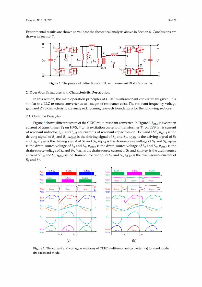
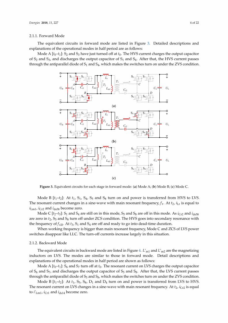

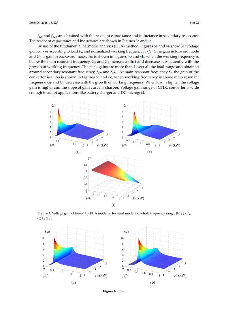
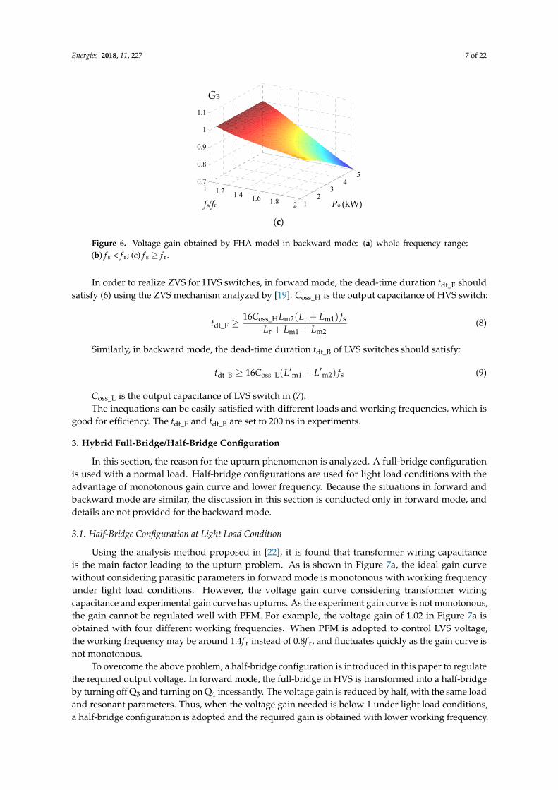
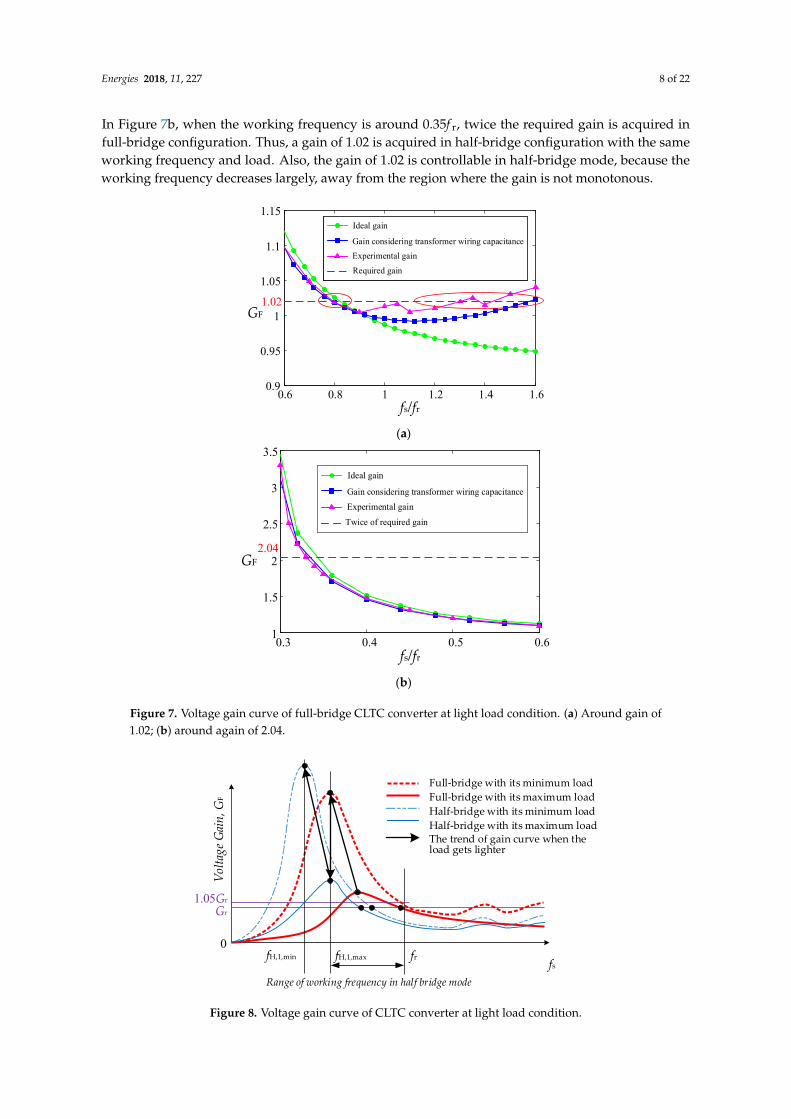
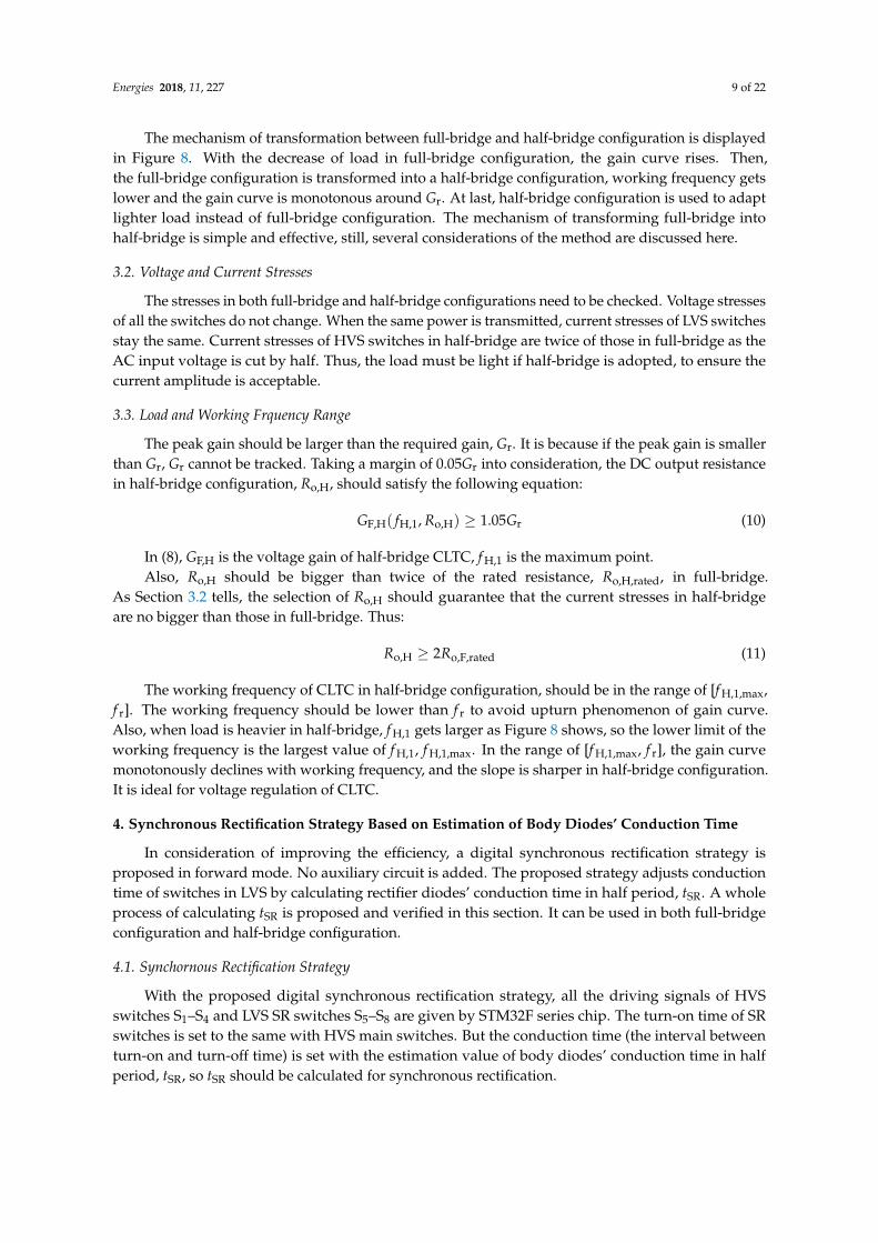
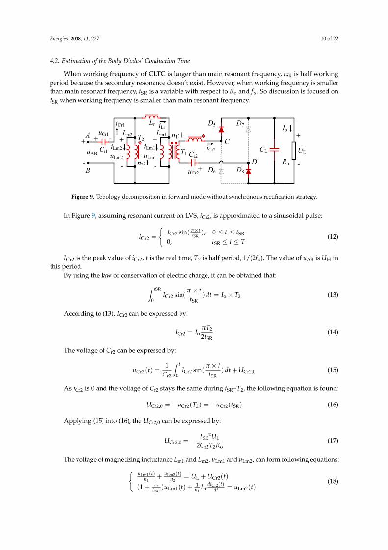

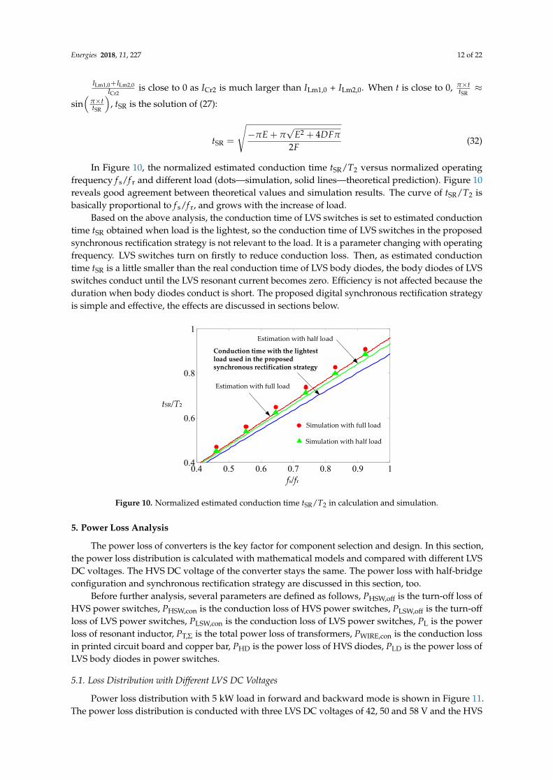
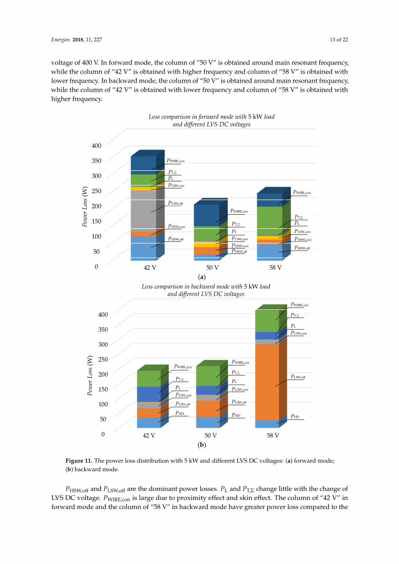

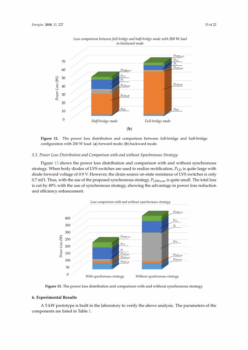
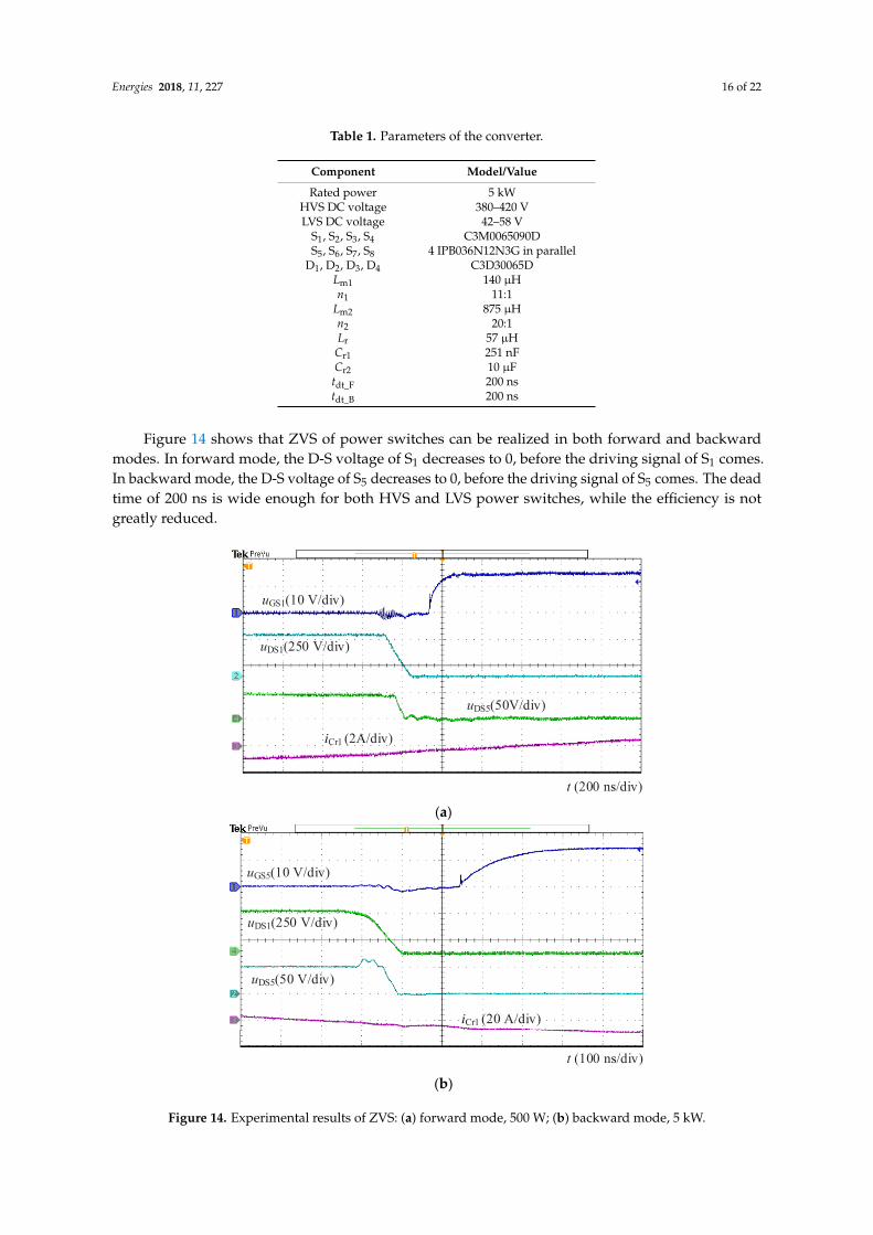
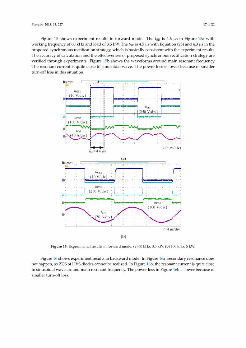
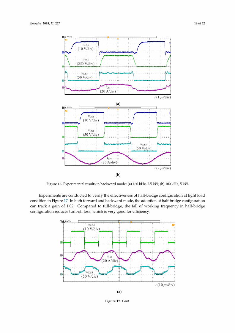
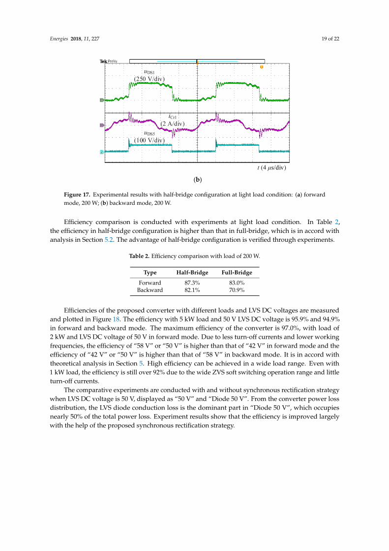
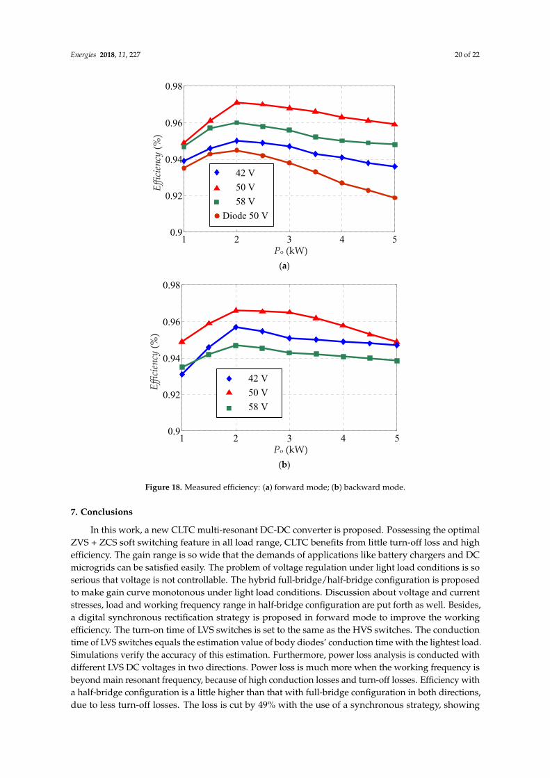


![Loss Modelling and Experimental Verification of A 98.8% Efficiency Bidirectional … · 2018-09-09 · A 1 kW resonant bidirectional converter is presented in [6] with an efficiency](https://static.documents.pub/doc/80x56/5f7034406d30cb11127d99a5/loss-modelling-and-experimental-verification-of-a-988-efficiency-bidirectional.jpg)


