38
RIGA TECHNICAL UNIVERSITY Deniss STEPINS STUDY AND QUALITY IMPROVEMENT OF FREQUENCY MODULATED SWITCH-MODE POWER CONVERTERS Summary of doctoral thesis Riga 2011

RIGA TECHNICAL UNIVERSITY
Deniss STEPINS
STUDY AND QUALITY IMPROVEMENT OF
FREQUENCY MODULATED SWITCH-MODE POWER
CONVERTERS
Summary of doctoral thesis
Riga 2011

RIGA TECHNICAL UNIVERSITY
Faculty of Electronics and Telecommunications
Institute of Radioelectronics
Deniss STEPINS
STUDY AND QUALITY IMPROVEMENT OF
FREQUENCY MODULATED SWITCH-MODE POWER
CONVERTERS
Summary of doctoral thesis
Scientific supervisor
Dr. habil. sc. ing., professor
J. JANKOVSKIS
Riga 2011

UDK 621.314.064 (043.2)
St 365 s
Stepins D. Study and quality improvement of
frequency modulated switch-mode power
converters. Summary of doctoral thesis.-
R.:RTU, 2011.- 37 p.
Printed according to the decision of FET
promotion council „RTU P-08” on March 2,
2011, protocol No 2.
This work is supported by the European Social Fund within the National Program “Support for the
carrying out doctoral study program’s and post-doctoral researches” project “Support for the
development of doctoral studies at the Riga Technical University”.
ISBN

A DOCTORAL THESIS SUBMITTED TO RIGA TECHNICAL UNIVERSITY
IN FULFILLMENT OF THE REQUIREMENTS FOR THE DEGREE OF
DOCTOR OF SCIENCE IN ENGINEERING
The doctoral thesis for the degree of doctor of science in engineering will be
presented in the auditorium 210 at Riga Technical University, Faculty of Electronics and
Telecommunications, 12 Azenes street, on the 9th
of June 2011, at 16:30 p.m.
OFFICIAL REVIEWERS
professor, Dr.sc.ing. Guntars Balodis
Faculty of Electronics and Telecommunications, Riga Technical University
Dr.phys. Alberts Kristiņš
Institute of Solid State Physics, University of Latvia
Dr.sc.ing. Leonards Latkovskis
Institute of Physical Energetics, Department of Power Electronics
CONFIRMATION
I confirm that the doctoral thesis, submitted for the degree of doctor of science in
engineering at the Riga Technical University, is my own original work. The doctoral thesis
has not been submitted for a degree at this or any other university.
Deniss Stepins …………………………….(Signature)
Date: ………………………
The doctoral thesis is written in Latvian, contains introduction, three chapters,
conclusions, references, 9 appendices, 108 figures, 144 pages in total. A list of references
consists of 122 sources.

Contents
1. INTRODUCTION.............................................................................................................5 Topicality of the thesis.........................................................................................................5
Objectives of the thesis.......................................................................................................7
Scientific novelty and main results.....................................................................................8
Defendable theses................................................................................................................8
Research methodology........................................................................................................9
Practical significance..........................................................................................................9
Approbation and Publicity..................................................................................................9
Structure of the thesis........................................................................................................11
2. ELECTROMAGNETIC INTERFERENCE (EMI) OF SWITCHING POWER
CONVERTERS (SPC) AND ITS SUPPRESSION TECHNIQUES........................12
3. IMPROVING EFECTIVENESS OF THE USE OF FREQUENCY
MODULATION (FM) IN SPC...................................................................................14
4. STUDY OF FM IMPACT ON SPC PARAMETERS; IMPROVING QUALITY
OF SPC...........................................................................................................................19 4.1. Influence of FM on output voltage ripples................................................................19
4.2. Influence of FM on efficiency of SPC......................................................................24
4.3. Influence of FM on SPC input power quality...........................................................28
5. CONCLUSIONS............................................................................................................32
LIST OF MAIN SYMBOLS AND ABBREVIATIONS................................................34
REFERENCES.....................................................................................................................35

5
TOPICALITY OF THE THESIS
Nowadays switching power converters (SPC) are essential to electric power conversion
with high efficiency (linear regulators used widely in the past had very low efficiency and
therefore they are used rather rarely nowadays). SPC are necessary for power supplies of
electronic devices and systems, lighting equipment electronic ballasts, etc. [1,2,3]. A
switching power converter is essential part of power electronics that nowadays is very
important field of science and technology. Electrical power conversion principles, power
electronic components as well as converter topologies are continuously improving [1].
Modern SPC development trends are mainly increasing specific power and efficiency, as
well as reducing electromagnetic interference (EMI), output voltage ripples, improving
thermal conditions, etc.
Advantages of switching power converters in comparison with other power converters
(e.g. linear regulators) are mainly high efficiency (it can be higher than 90% for modern
SPC) and high specific power (recently it has exceeded 3kW/dm3) [1].
Despite their advantages, SPC have also their drawbacks. The main SPC disadvantages
are high EMI both conducted and radiated as well as high output voltage ripples. EMI in
SPC is caused mainly by rapidly switching power semiconductor devices with high current
(di/dt) and voltage (dv/dt) rate of change [4]. With the introduction of the international
electromagnetic compatibility directives (e.g. CISPR 22), there is an increasing awareness
of the EMI problems of SPC [5]. The classical ways of mitigation of these problems usually
include the application of appropriate design of SPC (e.g. the use of input and output filters,
correct design of printed circuit boards, grounding, shielding, etc) and the use of soft
switching techniques [6-10]. However the techniques can substantially increase SPC size
1 1.5 2 2.5 3
x 105
-3
-2
-1
0
Fig. 1.1 Spectra of unmodulated and FM switching waveform.

6
and cost.
Another successful approach for EMI reduction known as spread spectrum has been
developed over the last two decades. It is based on modulating the switching frequency in
random, chaotic or periodic manner [5,11,12]. As a result, energy of discrete harmonics of
unmodulated switching frequency is spread over a wider frequency range, thus peak EMI
levels are significantly reduced [6] (as it can be seen in Fig. 1.1). The first publications on
the use of the spread spectrum to reduce EMI in electronics (e.g. [13-15]) appeared in mid
1990s [6]. Over the last 15 years spread spectrum has been extensively used not only for
EMI reduction in microprocessor systems and traditional SPC [5,6,11,13,14,16,19,20,27]
but also in power factor correctors [21,22], lighting equipment electronic ballasts and
inverters [23,24], and even in D class audio amplifiers [25]. It should be noted that despite
the fact that random or chaotic frequency modulation techniques are sometimes applied to
SPC because of better conducted EMI attenuation, periodic FM has several advantages:
firstly, spectrum of signal, which frequency is modulated by periodic signal (sinusoidal,
triangular, etc), is discrete, while that for random FM is continuous [6]; secondly, periodic
FM can be implemented easily and, thirdly, periodic FM introduces appreciably lower low
frequency ripples in output voltage of SPC [11]. In the research SPC with periodic FM will
be investigated, however some results can also be used for the other FM techniques.
Despite the fact that FM can reduce conducted EMI, it could be sufficiently ineffective
for EMI reduction with specific modulating signal m(t) parameters. It is shown in [23] that
amplitude modulation (AM) of electronic ballast output current can result in distortion and
asymmetry of the sideband of switching frequency (fsw) fundamental harmonic and
consequently worsen effectiveness of the use of FM for EMI reduction. In our research the
similar effect has also been observed for power factor correctors [21] and boost SPC [20].
To solve the problem in electronic ballasts, double-slope sawtooth modulating waveform
was proposed in [23]. Using the waveform the sideband asymmetry can be effectively
neutralized and conducted EMI attenuation can be improved at least by several dB [23].
However it is proved in our research that the technique is only effective for one combination
of modulating signal and power circuit components parameters. This means that this
technique is not optimal for other values of the parameters. That is why we, firstly, examine
if this method can be applied for input EMI reduction in other SPC topologies, and
secondly, we improve effectiveness of the use of the technique by optimizing it.
Despite its advantages FM similarly to other EMI suppression techniques has also its
drawbacks:
• increase in peak-to-peak output voltage ripples [6,11,12,16,27-30];

7
• in addition to “natural” high-frequency (HF) output voltage ripples, low-frequency
(LF) ripples (and LF harmonics) arise [6,11,27-30];
• deterioration of input power quality that is mainly important for AC mains-operated
SPC [6,18,22,24,31];
• possible decrease in efficiency [6,18,22,24,32].
Since the disadvantages are very important in SPC, then negative effect of FM on the
SPC performance should be examined and reduced. After analyzing scientific publications
related to the similar problems it is revealed that the publications have many drawbacks
such as:
• research results are mainly based on experiments (without appropriate theoretical
analysis);
• the main causes of the problems are not revealed;
• for the most part, the publications consider only the use of FM in unregulated SPC;
• recommendations to solve the problems effectively are not proposed in the
publications.
That is why we will try to examine the problems deeply in the research.
OBJECTIVES OF THE THESIS
The main aim of the doctoral thesis is to improve effectiveness of the use of FM in SPC,
to examine and reduce the negative effects of the technique on input and output power
quality as well as efficiency of SPC.
In order to achieve the aim, main tasks of the research are:
• to examine the influence of modulating signal and power stage circuit parameters on
EMI attenuation using periodic FM;
• to improve input EMI attenuation in FM SPC using optimized double-slope
modulating waveform;
• to investigate effect of FM on SPC output voltage ripples and to reduce them;
• to investigate negative effect of FM on the efficiency of SPC and to propose some
recommendations to increase it;
• to examine negative effect of FM on SPC input power quality and to improve it.

8
SCIENTIFIC NOVELTY AND RESEARCH RESULTS
Novelty of the doctoral thesis and the main research results are related to improvement of
usefulness of FM technique for EMI suppression in SPC and to reduction of negative effects
of FM on important FM SPC characteristics. The results obtained and novelties mainly are
as follows:
• effectiveness of the use of FM for maximum EMI suppression in FM SPC is
appreciably improved by using optimized double-slope modulating waveform;
• a procedure for the calculation of double-slope modulating waveform optimum
parameters values is developed to get maximum conducted EMI attenuation in FM
SPC;
• formerly unknown causes of the increase in output voltage ripples and deterioration
of input power quality of regulated FM SPC in both continuous conduction mode
(CCM) and discontinuous conduction mode (DCM) are revealed;
• original recommendations for reducing output voltage ripples and improving input
power quality of FM SPC are proposed;
• original recommendations for improving the efficiency of FM SPC are proposed and
verified;
• a procedure for the calculation of the output voltage ripples and the efficiency in FM
SPC is developed. The procedures could be useful for FM SPC design and
optimization;
• original research on the negative effect of FM on SPC output voltage ripples and
input power quality in DCM is conducted;
• original solution to get small difference between the switching delays and therefore
very small LF ripples in CCM is proposed and verified.
DEFENDABLE THESES
For a defense of the doctoral thesis the following theses are proposed:
1) conducted EMI attenuation in FM SPC can be increased by using optimized dual-
slope modulating waveform or selecting the switching frequency according to
recommendations proposed. In order to get maximum EMI attenuation, optimum
values of double-slope modulating waveform parameters should be calculated
according to the procedure proposed;

9
2) output voltage ripples of FM SPC can effectively reduced using recommendations for
selecting modulating signal, power stage and control unit parameters;
3) recommendations proposed can help to mitigate negative effect of FM on the
efficiency of FM SPC;
4) input power quality of FM SPC can be significantly improved using the
recommendations proposed.
RESEARCH METHODOLOGY
In the doctoral thesis, FM SPC have been studied theoretically, experimentally and using
computer simulations. Initially the problems were analyzed theoretically and analytical
expressions were also derived. Theoretical results have been verified using the computer
simulation. Further the results obtained have been verified experimentally.
PRACTICAL SIGNIFICANCE
The results obtained and the recomendations proposed could be applied for designing
high-quality FM SPC as well as for their development.
APPROBATION AND PUBLICITY
The research results have been presented in 9 international scientific conferences:
• IEEE International Symposium on Industrial Electronics (IEEE ISIE10), Bari, Italy,
July 4-7, 2010.
• International Biennial Baltic Electronics Conference (BEC2008), TUT, Tallinn,
Estonia, Oct. 6-8, 2008.
• International Biennial Baltic Electronics Conference (BEC2010), TUT, Tallinn,
Estonia, Oct. 4-6, 2010.
• The 14th International Conference „Electronics ‘10”, Kaunas, Lithuania, May 18-20,
2010.
• The 12th International Conference „Electronics ‘08”, Kaunas, Lithuania, May 20-22,
2008.
• The 13th International Conference „Electronics ‘09”, Kaunas, Lithuania, May 12-14,
2009.

10
• The 10th International Conference „Electronics ‘06”, Kaunas, Lithuania, May 23-25,
2006.
• The 9th International Symposium on Electronics and Telecommunications
(ISETC2010), Timisoara, Romania, Nov. 11-12, 2010.
• The 50th RTU International Conference, Rīga, Latvija, 2009. gada 14.-16. Oktobrī.
The research results have been published in 12 internationally recognized sources:
1. Stepins D. Analysis of Output Voltage of Switching Frequency Modulated DC-DC
Converter Operating in Discontinuous Conduction Mode // Proceedings of IEEE
International Symposium on Industrial Electronics (IEEE ISIE10), Bari, Italy, July 4-
7, 2010. – pp. 670-675.
2. Stepins D. Examination of influence of periodic switching frequency modulation in
dc/dc converters on power quality on a load // Proceedings of the 11th Biennial
Baltic Electronics Conference, Tallinn, Estonia, Oct. 6-8, 2008. – pp. 285-288.
3. Stepins D. Examination of Power Converters with Modulated Switching Frequency //
Electronics and Electrical Engineering. - 9(105). – 2010. - pp. 33.-38.
4. Jankovskis J., Stepins D., Pikulins D. Improving effectiveness of the use of
frequency modulation in power converters // Proceedings of the 12th Biennial Baltic
Electronics Conference, Tallinn, Estonia, Oct. 4-6, 2010. – pp. 327-330.
5. Stepins D. Improving EMI attenuation in a frequency modulated boost converter //
RTU zinātniskie raksti. 7. sēr., Telekomunikācijas un elektronika. - 9. sēj. (2009),
17.-23. lpp.
6. Jankovskis J., Stepins D., Tjukovs S., Pikulins D. Examination of Different Spread
Spectrum Techniques for EMI Suppression in dc/dc Converters // ELECTRONICS
AND ELECTRICAL ENGINEERING. - 6 (86). – 2008. – pp. 60.-64.
7. Jankovskis J., Stepins D., Pikulins D. Lowering of EMI Noise in Boost Type PFC by
the use of Spread Spectrum// ELECTRONICS AND ELECTRICAL
ENGINEERING. - 6 (94). – 2009. – pp. 15.-18.
8. Jankovskis J., Stepins D., Pikuļins D. Efficiency of PFC Operating in Spread
Spectrum Mode for EMI Reduction // Electronics and Electrical Engineering. - 7. –
2010. – pp. 13.-16.
9. Jankovskis J., Stepins D., Pikuļins D. Effects of Increasing Switching Frequency in
Frequency Modulated Power Converters // Proceedings of the ”2010 9th
International Symposium on ELECTRONICS AND TELECOMMUNICATIONS”,

11
Timisoara, Romania, November, 11-12, 2010. – pp. 115-118.
10. Jankovskis J., Stepins D. An Examination of Parasitic Processes in DC/DC Power
Converters // ELECTRONICS AND ELECTRICAL ENGINEERING. - 4(68). -
2006. – pp. 15.-18.
11. Stepins D. On the Figures of Merit for Planar Spiral Inductors // RTU zinātniskie
raksti. 7. sēr., Telekomunikācijas un elektronika. - 7. sēj. (2007), 16.-18. lpp.
12. Stepins D. Performance-Analysis-Based Examination of Planar Spiral Inductors //
Materials of the 4th International Young Scientist Conference “Modern Issues in
Radio Engineering and Telecommunications”, Sevastopol, Ukraine, April 21-25,
2008. – pp. 312.
Four publications (1,2,4,9) are also available in IEEEXplore Digital Library.
STRUCTURE OF THE THESIS
The doctoral thesis consists of introduction, three chapters, conclusions, references and
appendices. Topicality, scientific novelty and objectives of the thesis as well as literature
review, approbation and practical importance are provided in the introduction. The second
chapter gives a brief review of EMI modes, international EMI specifications, traditional
conducted EMI suppression techniques for SPC and their advantages and disadvantages, as
well as spread spectrum technique. The third chapter presents a brief review of frequency
modulation, considers spectrum of a periodic rectangular pulse train as well as the
attenuation. Theoretical study of EMI in FM SPC is performed in the chapter 3.2. The use
of double-slope sawtooth modulating waveform for increasing EMI suppression is analyzed
in the chapter 3.3. Chapter 3.4 provides results of the experimental verification, but chapter
3.5 draws some conclusions. The fourth chapter is dedicated to the negative effect of FM on
crucial FM SPC quality characteristics: peak-to-peak output voltage ripples (chapter 4.1),
the efficiency (chapter 4.2) and input power quality (chapter 4.3). Appendices show
SIMULINK models for both unregulated and regulated FM SPC with buck and boost
topologies, present regulated FM buck converter schematic diagram used in the
experiments, and present the calculation procedures for peak-to-peak output voltage ripples
and efficiency of FM SPC.

12
2. ELECTROMAGNETIC INTERFERENCE OF SWITC-MODE POWER
CONVERTERS AND ITS SUPPRESSION TECHNIQUES
In the second chapter EMI modes, its causes in SPC and international EMI specifications
are discussed briefly. A brief review of traditional conducted EMI suppression techniques
for SPC and their advantages and disadvantages, as well as novel technique, known as
spread spectrum, is presented in this chapter.
SPC are usually one of the main contributors to EMI. Since EMI generated by SPC can
disturb normal operation of other electronic equipment, EMI suppression is of importance
when designing SPC. EMI in SPC is caused by rapidly switching power semiconductor
devices with high di/dt, dV/dt [8]. As a result switching waveform spectrum consists of
multiple switching frequency (fsw) harmonics that occupy wide bandwidth. Since fsw of SPC
are rather high (they can range from several tens of kHz up to several MHz), the problem is
very important [7,10,15]. Conducted EMI is more pronounced at lower frequencies, but
radiated EMI: at higher frequencies. That is why conducted EMI is usually measured in the
frequency range from 150 kHz to 30 MHz, but radiated EMI – from 30 MHz to 1 GHz [4].
There are various standards that specify EMI measurement limits. One of the world-wide
accepted standards is CISPR Publication
22 [4].
Conducted EMI as such can travel
through input wires to a power line and
consequently disturb normal operation of
other electronic equipment connected to
the same line. For conducted EMI
measurements a line impedance
stabilization network (LISN) and EMI or
spectrum analyzer are used. LISN is usually connected between a power line and SPC under
test (see Fig. 2.1). The standards also specify EMI analyzer input filter bandwidth, also
known as resolution bandwidth (RBW), for different EMI measurement ranges. For
example, according to CISPR 22 conducted EMI measurements should be performed in the
frequency range from 150 kHz to 30 MHz with RBW=9kHz, but as per CISPR 16
specifications the measurements should be performed in the frequency range from 9 kHz to
150 kHz with RBW=200 Hz [10].
Fig. 2.1 Typical EMI measurements block
diagram.

13
Conducted EMI can be categorized into two separate modes of current flow: differential
mode and common mode noise [4]. Differential mode EMI is due to SPC input current, but
common mode EMI is mainly caused by parasitic capacitances to ground and rapidly
switching power transistor with high dv/dt.
Classical ways for suppressing conducted and radiated EMI are usually include the use
of input EMI filters, that can effectively reduce both differential and common mode EMI;
special snubber RC or RCD circuits, that can be connected across power transistors or
diodes; ferrite beads, that attach easily to SPC input/output wires and power components
terminals; shielding of SPC for suppressing radiated emissions; correct design of printed
circuit board according to electromagnetic compatibility requirements; soft switching
techniques [8,9].
Each EMI suppression technique has its own drawbacks. For instance, despite the fact
that passive input filters can effectively reduce conducted EMI, they are highly responsible
for increasing size, weight, cost of SPC and decreasing their efficiency.
Considerable recent attention has been focused on the use of another successful approach
for EMI reduction, known as spread spectrum. The technique, in fact, has been adopted
from communication theory and, as it was mentioned before, it has been used for EMI
suppression in microprocessor systems, as well as various SPC and recently even in D class
amplifiers [6,8,25]. As a result, energy of discrete harmonics of unmodulated switching
frequency is spread over a wider frequency range, thus peak EMI levels are significantly
reduced [6], as it can be seen in Fig. 1.1. Spread spectrum can help to reduce not only
conducted EMI but also radiated one. Spreading the spectrum can be achieved through
different ways: one of the most effective techniques is frequency modulation (FM) [5,11].
In this work, frequency modulated SPC are to be examined, because FM can give better
EMI attenuation than other spread spectrum techniques. In general the switching frequency
can be modulated periodically, chaotically or in random manner. It is mentioned in several
publications (e.g. [11]), that random and chaotic FM can give better EMI attenuation, than
periodic FM (under the assumption that frequency deviation is the same). However periodic
FM has several advantages. For example, it can give lower output voltage ripples (mainly
LF ripples) and can be implemented easier, than chaotic or random FM. This PhD thesis is
dedicated to SPC with periodic FM, nevertheless several results can be applied for other FM
techniques.

14
3. IMPROVING EFECTIVENESS OF THE USE OF FM IN SPC
The third chapter presents a brief review of frequency modulated signals and their main
parameters, considers spectrum of a periodic rectangular pulse train as well as the
attenuation that can be achieved using FM in SPC. Original theoretical research on EMI in
FM boost SPC has been done taking into account LISN and power stage parasitic
parameters. In the third chapter it also proved that optimized double-slope modulating
signal can substantially improve usefulness of FM and increase input EMI attenuation in
traditional SPC. The procedure for the calculation of double-slope modulating waveform
optimum parameters values to get maximum conducted EMI attenuation in FM SPC is also
developed in the chapter.
FM rectangular pulse train representing approximately, for example, MOSFET control
signal or several other power stage voltages responsible for EMI can be expressed as:
))],(2[cos()( ttfsignts sw θπ += (3.1)
where fsw is central switching frequency; θ(t) – time-dependent phase angle.
Spectrum of rectangular pulse train which frequency is modulated by a sine wave can
be calculated using the Bessel functions. For other periodic modulating waveforms m(t),
Fourier series in complex exponent form should be used. It should be noted that if fsw/fm (fm
is modulating frequency) is integer number, then FM signal period equals m(t) period Tm.
FM rectangular pulse train spectrum is made up of sidebands comprising side frequencies
nfsw±kfm (n, k are integers) [33], as it is shown in Fig. 3.1. Attenuation due to FM is different
for each individual unmodulated fsw harmonic (as it can be seen in Fig. 3.1.). Since
unmodulated fundamental harmonic of fsw usually is dominant in conducted EMI spectrum,
then it makes sense to estimate the attenuation just for this harmonic. The attenuation can be
1 2 3 4 5 6 7 8 9
x 105
20
40
60
80
100
120
140
Fig. 3.1 Spectrum of unmodulated and FM rectangular pulse train (fsw=150kHz; fm=2kHz;
frequency deviation ∆fsw=20kHz; m(t) is sawtooth waveform).

15
defined as the difference expressed in dB between amplitude of unmodulated fundamental
harmonic of fsw |C1|=2|d1| and maximum amplitude of the first sideband harmonics of FM
signal [24]:
=
))(max(
||log20
mod1
110
fS
CA , (3.2)
where |S1mod(f)| is the amplitude spectrum of the first sideband.
The higher modulation index β=∆fsw/fm is, the better fsw harmonics amplitude attenuation
is [6,11]. Notice that the attenuation is independent on fsw. The attenuation that can achieved
by frequently used modulating waveforms (i.e. sine, sawtooth, triangle) is almost the same
up to β=10. For higher β values, sawtooth m(t) gives the best attenuation, but sine wave –
the worst [6]. Increase in the attenuation for sufficiently high β values is slow. FM signal
spectrum of the first sideband is symmetrical to fsw.
Since rectangular pulse trains are only analyzed in many publications (e.g. [6,11,15])
about the use of FM for EMI suppression, it hinder us to reveal the causes worsening the
effectiveness of FM in SPC. That is why in the research EMI is analyzed taking in account
LISN and FM SPC power stage parasitic parameters. For this purpose total EMI model [35]
shown in Fig. 3.3 is used. The model can give us a possibility to derive transfer function
between equivalent EMI source Vs and LISN radio frequency (RF) output voltage VLISN:
+−
+++++
++++
+=
)(2)55/()5)(2/25(
)55/()5)(2/25(
50
50)(
3535
3535
5 LCin
Cin
LCLCCh
LCLC
CEMI
ZZ
Z
ZZZZZ
ZZZZ
ZfK
,
(3.3)
where ZC5, ZCh, ZL3 are complex impedances.
In making analysis of VLISN spectrum for different fsw values it is concluded that the first
harmonic amplitude attenuation AEMT depends not only on β (as it is for FM rectangular
Fig. 3.2. Boost SPC schematic diagram with LISN.

16
pulse train) but also on fsw. The frequency determines the sideband location in the frequency
domain as it can be seen in Figs. 3.4 and 3.5. If the sideband is in the range where
|KEMI(f)|changes steeply (this mainly corresponds to the LF range where differential-mode
EMI is dominant), then difference between A and AEMT (∆A) is high and in turn the
effectiveness of the use of FM is low. If the sideband is in the range where |KEMI(f)| changes
slowly (this mainly corresponds to higher frequencies), then ∆A is small. The best results
Fig. 3.3. Total boost converter EMI model [35].
1 2 3 4 5 6
x 105
-65
-60
-55
-50
-45
|KE
MI(
f)|,
dB
0.5 1 1.5 2 2.5 3 3.5 4 4.5 5
x 105
10
20
30
40
50
60
70
80
AEMT
VL
ISN
spek
trs,
dB
µV
Frekvence, Hz 1 2 3 4 5 6 7 8 9 10
x 105
10
20
30
40
50
60
70
80
Frekvence, Hz
VL
ISN
spek
trs,
dB
µV
VL
ISN
spec
trum
, dB
µV
VL
ISN
spec
trum
, dB
µV
Fig. 3.4 Transfer function |KEMI(f)|. Effectiveness of the use of FM depends on the location of the
fundamental harmonic sideband.

17
can be achieved when the sideband is located in the range where common-mode and
differential-mode EMI are comparable. In the range |KEMI(f)|is almost independent on the
frequency. When increasing ∆fsw, the difference ∆A between AEMT and A also increases.
However the difference is very small for low values of ∆fsw. For a given modulation index
sinusoidal FM gives the highest ∆A but triangular FM the lowest ∆A. The difference ∆A
decreases slightly for higher fm.
It should be noted that sometimes selection of fsw depends on other SPC parameters,
mainly the efficiency. That is why it is of importance to propose an alternative solution to
get maximum AEMT (or minimum ∆A) for given m(t) parameters without changing fsw. A
technique to reduce AM and fundamental fsw harmonic sideband asymmetry in FM
electronic ballast output current was proposed in [23]. The technique is based on the use of
double-slope sawtooth modulating waveform shown in Fig. 3.6. Since the technique was not
applied to other SPC topologies for conducted input EMI suppression, then one of our tasks
is to verify and prove that the method is also effective in FM SPC for input conducted EMI
suppression and improving effectiveness of the use of FM. The asymmetry of the sidebands
can be appreciably reduced using
different slopes for the sawtooth
modulating waveform [23] (see
Fig. 3.6). The slopes can be
adjusted by changing t0 values. It
is noted in [23] that output current
fundamental fsw harmonic
sideband asymmetry and AM can
0 1 2 3 4
x 104
0
2
4
6
8
10
12
14
16
18
Fig. 3.5 EMI attenuation of fundamental fsw harmonic amplitude both for FM rectangular
pulse train (A) and FM SPC VLISN (AEMT).
Fig. 3.6. Double-slope sawtooth modulating waveform.

18
be reduced if t0=0.35Tm. However as it is proved in the doctoral thesis, the sideband
asymmetry and in turn ∆A are dependent both on parameters of the power stage components
including parasitics and modulating signal and switching signal parameters. Thus t0=0.35Tm
can give minimum ∆A or maximum AEMT only for a single combination of the parameters.
For other values of the parameters it can even worsen AEMT in comparison with traditional
sawtooth waveform with t0=0.5Tm. That is why one more task of the research is to develop a
procedure to calculate optimum t0 to get minimum ∆A or maximum AEMT for a given m(t)
and SPC parameters values, and also examine if the technique does not worsen EMI
attenuation at higher frequencies. It should be noted that not only modified sawtooth but
also other m(t) can be used provided that the similar modification is done. Changing t0 value
with small step and calculating VLISN spectrum using the procedure and the expressions for
the spectrum calculation derived in the thesis, optimum t0 values can be found. Thus we can
conclude that the use of the optimized double-slope modulating waveform can appreciably
improve AEMT and in turn reduce ∆A, and improve FM usefulness in FM SPC, as it can be
seen in Fig. 3.7 and 3.8 (note that AEMT1 denotes EMI attenuation using modified m(t)). It is
worth noting that the technique does not worsen EMI attenuation at higher frequencies.
1 2 3 4 5 6 7 8
x 105
10
20
30
40
50
60
70
80
1 2 3 4 5 6 7 8
x 105
10
20
30
40
50
60
70
80
Fig. 3.7. Calculated VLISN spectrum for unmodulated and FM SPC. Modulation parameters:
∆fsw=30kHz, fm=1kHz, fsw=80kHz, (a) t0=0.5Tm; (b) t0=0.29Tm.
0 1 2 3 4
x 104
0
5
10
15
20
Fig. 3.8. Calculated AEMT (for t0=0.5Tm), A and AEMT1 (using optimum t0) as a function of
∆fsw for fm=1 kHz and fsw=80kHz.

19
4. STUDY OF IMPACT OF FM ON SPC PARAMETERS; IMPROVING
QUALITY OF SPC
4.1. Influence of FM on output voltage ripples
In the chapter 4.1 the output voltage ripples both for unregulated and regulated SPC in
CCM and DCM are investigated. Expressions to calculate the peak-to-peak output voltage
ripples in both CCM and DCM are derived. The results obtained are confirmed
experimentally. Original recommendations to reduce the output voltage ripples effectively
are proposed and verified. A circuit to mitigate the LF ripples in CCM is also developed.
It is measured in several publications (e.g. [6,11,16]) that FM SPC output voltage ripples
increase due to FM. Thorough examination of FM effect on the output voltage ripples of
unregulated (operating in open-loop) FM SPC in CCM was performed only in [27] and
independently in our publications ([17,30] in CCM and [29] in DCM). Although the main
causes of the increase in the output voltage ripples are revealed in [27] for unregulated buck
FM SPC, effect of FM on the ripples of regulated (operating in closed-loop) SPC and FM
SPC operating in DCM are not investigated in the publication. Moreover, expressions or
procedure to calculate the output voltage ripples are not derived and recommendations to
mitigate the ripples effectively are not proposed in [27].
In making thorough examination we have concluded that FM increases the output voltage
ripples both in CCM and DCM. In general the ripples consist of HF switching ripples and
LF ripples with fm, as it is shown in Fig. 4.1. Generally an envelope of the total ripples in
FM SPC is as follows:
)()(~min)()(~max tAtvtAtvVHFLFHFLFpofmp
−−+=− , (4.1)
0.0232 0.0234 0.0236 0.0238 0.024
-0.01
-0.005
0
0.005
0.01
20.2 20.4 20.6 20.8 21
4.84
4.845
4.85
4.855
4.86
4.865
4.87
4.875
Fig. 4.1. Calculated envelope of the output voltage ripples (a) un simulated output voltage ripples (b)
for buck SPC in CCM taking in account |td|=110ns. Parameters: Cout=330uF; L=125uH; Vin=10V; m(t)-
sine; fm=2kHz; ∆fsw=30kHz; fsw=76kHz; rcout=0.04Ω; rL=0.12Ω; D=0.5; output load Rout=10Ω.

20
where vLF(t) is LF ripples; AHF(t) is envelope of the HF ripples. An expression for the
envelope of the HF ripples can be derived using an expression for the unmodulated SPC
ripples. For this purpose constant fsw should be substituted with instantaneous switching
frequency fsw(t). So the HF ripples, for instance, for FM SPC with typical output electrolytic
capacitor in CCM is:
)(2
)1()(
tLf
DVrtA
sw
outcoutHF
−= , (4.2)
where rcout is equivalent series resistance of the output capacitor (ESR); D is average duty
ratio; Vout is DC output voltage.
The instantaneous switching frequency is:
)()( tmfftf swswsw ∆+= . (4.3)
The cause of increasing the HF ripples is natural: minimum switching frequency
fswmin=fsw-∆fsw gives maximum peak-to-peak HF ripples [27,30]. Relative increase in peak-to-
peak HF ripples in comparison to ripples of the unmodulated SPC is lower for higher fsw but
the same ∆fsw. Increase in the HF ripples of FM SPC with typical electrolytic capacitors is
much less pronounced for boost SPC or related topologies (such as flyback or buck-boost)
where output capacitor current also depends on power inductor or transformer secondary
DC current ILavg than in buck SPC or related topologies where the HF ripples depend only
on the power inductor AC current. This means that from the HF ripples point of view, FM is
much less harmful in boost SPC or related topologies than in buck SPC.
The genuine cause of the LF ripples for FM SPC in CCM is nonzero difference |td|
between the switching delays [17,27,30]. SPC switching delays are mainly related to power
transistor switches, their drivers and logic circuits (e.g. flip-flops) of pulse width modulated
(PWM) integrated circuits. Sometimes the switching delays are intentionally applied for
SPC control signals, for instance, in synchronous buck SPC where the delay is necessary for
both power transistors not to be in on state simultaneously because it can cause high shoot-
through current. If |td|≠0, then FM causes parasitic PWM in CCM and consequently
instantaneous duty ratio d changes in time with fm. This effect causes high LF ripples in the
output voltage. In the doctoral thesis a general expression for the calculation of the LF
ripples of regulated FM SPC in CCM is derived in operator form considering nonzero |td| as
follows:
))(1/()()(||))(1/()()(
~)(~ sTsHsmftsTsHsdsv coswdcoLF +∆=+=
, (4.4)
where Hco(s) is control-to-output transfer function; T(s) is open loop gain. Using the Laplace
transform of the equation (4.4), a steady-state LF ripples vLF(t) can be calculated in time
domain. Note that only the steady-state solution is of interest and that m(t) is a periodic
function of time. The LF ripples in the time domain for sinusoidal FM can be easily
obtained from (4.4) as follows:

21
)2(1
)2(
)2(1
)2(arg2cos||)(~
m
mco
m
mcomswdLF
fjT
fjH
fjT
fjHtffttv
π
π
π
ππ
+
++∆= . (4.5)
It follows that the LF peak-to-peak ripple for sinusoidal FM in CCM is:
)2(1
)2(||2
m
mcoswdpLFp
fjT
fjHftV
π
π
+∆=− . (4.6)
From this results the conclusion that the LF peak-to-peak ripple VLFp-p is directly
proportional to |td| and ∆fsw, and it also depends on fm and m(t). If |td|=0, then output LF
ripples are nullified even in regulated SPC. It follows that Vofmp-p depends only on the HF
ripples.
Recommendations for decreasing the output voltage ripples in CCM.
1) To neutralize the LF ripples, the power MOSFET control circuit should be designed so
that |td| is low. This can be achieved, for instance, using two MOSFET drivers with delay
RCD circuit connected between them, as it is shown in Fig. 4.2. It should be noted that the
technique does not require to increase cost and printed circuit board size, because modern
MOSFET drivers integrated circuits include two drivers with individual outputs.
2) If it is possible to choose FM SPC topology, then it is better to use boost or related
topologies where output capacitor current depends on ILavg substantially.
3) In regulated FM SPC, fm should be far away from fmax at which |Hco(s)/(1+T(s))| is
maximal. Note that fmax in buck SPC is equal to output filter resonance frequency, as it is
shown in Fig. 4.3.
4) As the modulating signal triangular m(t) should be used. It is recommended to use
sawtooth m(t) when fm>fmax. The sawtooth m(t) should not be used, if its first harmonic is in
Fig. 4.2. An artificial delay circuit to get small |td| and the LF ripples.

22
the range where |Hco(s)/(1+T(s))| rises.
FM causes the peak-to-peak output voltage ripple Vofmp-p to increase in FM SPC in DCM.
As it is for CCM, in DCM the ripples also consist of HF switching ripples and LF ripples
with fm. Moreover the output voltage spectrum consists of LF fm harmonics and side
frequencies. Similarly to CCM, in DCM fswmin also determines increase in peak-to-peak HF
ripples.
The cause of the LF ripples in DCM is not the same as in CCM: the LF ripples are due to
the fact that output voltage averaged to Tsw depends on fsw. This means that the LF ripples
are natural and independent on parasitic parameters as it is in CCM. The peak-to-peak LF
ripple for sinusoidal FM in DCM is:
( )
out
outinin
m
mout
sw
swpLFp
LV
VVVD
fjT
fjH
f
fV
−
+
∆≈−
2
2 )2(1
)2(
π
π , (4.7)
where Hout(j2πf) is output voltage to inductor current transfer ratio in DCM. It can be
concluded that VLFp-p is approximately proportional to ∆fsw and approximately inversely
proportional to fsw raised to the power of 2. This means that for constant ∆fsw, the higher fsw
is, the lower LF ripples are. In general, to derive the expressions of the output voltage LF
ripples for different SPC topologies and m(t), the expressions should be firstly derived for
LF ripples vLFunreg(t) in FM SPC using averaged models in DCM. Then using T(s) in DCM,
the LF ripples can be calculated for the regulated FM SPC. Note that VLFp-p also depends on
fm and m(t). In the regulated FM SPC, the lower fm is, the lower VLFp-p is.
Fig. 4.3. Regulated buck FM SPC transfer functions in CCM. Parameters: Cout=330uF; L=125uH;
∆fsw=30kHz; rc=0.04Ω; rL=0.12Ω; Rout=10Ω; fsw=80kHz; fcut=5kHz.
100
102
104
106
-60
-40
-20
0
20
40
frekvence, Hz
Pār
vad
es f
un
kci
ju m
od
uļi
, d
B
|Hco(s)|
|1/(1+T(s))|
|Hco(s)/(1+T(s))|
fmax

23
Recommendations for decreasing the output voltage ripples in DCM.
1) Keeping |td| as low as possible is not necessary in DCM, because it barely affects the LF
ripples in DCM. This can be deduced from the expression of power inductor current
averaged to Tsw for FM buck SPC operating in DCM:
( )
++⋅
−= )(2
)(2
22
tftDttf
D
LV
VVVi swdd
swout
outininL . (4.8)
It follows that the first term in the second bracket is the same as for FM SPC with td=0. The
second term is negligible DC term. But the third term is LF AC component due to nonzero
td. Considering typical |td| and FM parameters, it can be concluded that the third AC term is
much lower than the first AC term in the second brackets of (4.8).
2) To reduce the LF ripples in the regulated FM SPC in DCM, fm should be less than open-
loop gain cut-off frequency fcut at least several times, as it can be deduced from Fig. 4.4.
3) As the modulating signal triangular m(t) should be used. It is recommended to use
sawtooth m(t) when fm>fcut. The sawtooth m(t) should not be used, if its first harmonics is in
the range where Hfull(s) rises (when fm<fcut).
4) If it is possible to choose fsw, then the higher fsw is the better, because it allows us to get
lower VLFp-p. This is because, firstly, fcut can be increased; secondly, VLFp-p is inversely
proportional to fsw raised to the power of two.
Fig. 4.4. Regulated buck FM SPC transfer functions in DCM. Parameters: Cout=470uF; L=42.5uH;
∆fsw=30kHz; rcout=0.043Ω; rL=0.07Ω; Rout=30Ω; fsw=80kHz; fcut=6kHz.
101
102
103
104
105
-60
-40
-20
0
20
40
60
80
Pār
vad
es f
un
kci
ju m
od
uļi
, d
B
frekvence, Hz fcut
|Hout(s)|
|T(s)|
|Hfull(s)|=|Hout(s)|/|1+T(s)|

24
4.2 Influence of FM on efficiency of SPC
In the chapter 4.2 original study of influence of FM on SPC losses and the efficiency η is
presented. A procedure to calculate η in FM SPC is developed. Expressions to calculate the
losses and η for FM boost SPC in CCM are derived. The theoretical results are confirmed
experimentally. Recommendations to eliminate the negative effect of FM on η of FM SPC
are proposed and verified experimentally.
In making the analysis of the publications [6,18,22] about FM negative effect on SPC
losses and η, it has been concluded that there are severe ambiguities in understanding the
problem, mainly because the analysis is experimentally based without relevant theoretical
explanation. For instance, it is measured in [22] that η of FM 600W boost power factor
corrector (PFC) decreases by several percent due to the use of FM. The authors in [22]
explained this by increased losses in power inductor core. However the experimental
investigation of the same PFC in [6] showed that FM does not affect η. It is also
experimentally revealed in [18] that FM has no influence on η of FM 600W SPC. The
theoretical explanation of the problem is only presented in our paper [32]. The explanation
is also confirmed experimentally using FM PFC.
In making thorough examination of the problem it is concluded that losses of FM SPC
Plossmod can be calculated using the expression for unmodulated SPC losses Ploss as follows:
∫ ∑===
m swmT TT
kkswkswloss
m
loss
m
loss TTPT
dttpT
P0
/
1,,mod )(
1)(
1 (4.9)
where ploss(t) are instantaneous losses of FM SPC; Ploss(Tsw,k) are losses at k-th switching
period Tsw,k; Tsw is unmodulated SPC switching period; Tm is modulating signal period. Note
that the expression is only useful when Tm/Tsw is an integer number. In making detailed
examination, it is concluded that SPC total losses can be divided into three separate
components: losses independent on fsw (Pconst), linearly dependent losses (Plin(fsw)), and
losses nonlinearly dependent on fsw (Pnonlin(fsw)). It is follows that total losses in unmodulated
SPC are:
)()()( 21 swnonlinswswnonlinswlinconstloss fPfAAfPfPPP ++=++=, (4.10)
where A1 and A2 are the coefficients dependent on specific SPC topology. The coefficients
derived in the doctoral thesis, for instance, for boost SPC are as follows:

25
1)(2 ])1(/)1()1([ ArDDIDVRDDRRIP CoutLavgddonDSLDCconstLavg
=−+−+−++= (4.11)
swswfrLavgoutswlin fAfttIVfP 2)(2
1)( =+= (4.12)
where Vd is Schottky diode threshold voltage, RLdc is the power inductor DC resistance; Rd is
forward resistance of a diode;
RDS(on) is a power MOSFET on-
resistance; tr and tf are the power
MOSFET rise and fall times
respectively. Pconst mainly relates
to DC conduction losses, Plin(fsw)
mainly relates to switching
losses, but Pnonlin(fsw) mainly
relates to power inductor
magnetic core losses and AC
conduction losses. It is derived in
the doctoral thesis that the losses
in the unmodulated boost SPC
are as follows:
αβαβ
β
−−+=
+
++−+−++
=
swswsw
incm
sw
CinCoutdonDSLDCinswnonlin
f
A
f
A
fNS
DVVC
fL
rrDRDDRRDVfP
4
2
3
22
)(22
1
2
12
])1()1([)(
(4.13)
where rcin is input capacitor ESR; N is number of turns of power inductor; S is the magnetic
core cross-section area; α, β are Steinmetz equation empirical coefficients that are usually
listed in magnetic core material datasheets, e.g. [34]; Vc is the magnetic core volume.
Nonlinearly dependent losses are more pronounced at lower fsw, but linearly dependent ones
at higher fsw, that can also be seen in Fig. 4.5.
Equation (4.9) can be rewritten as:
∑=
++=swm
TT
kkswkswnonlin
mswloss TTP
TfAAP
/
1,,21mod )(
1 (4.14)
0 1 2 3 4 5
x 105
0
0.1
0.2
0.3
0.4
0.5
0.6
0.7
0.8
Loss
es, W
Fig. 4.5 Calculated Ploss and its components dependence on
fsw for unmodulated boost SPC in CCM with the powdered-
iron-core power inductor (L=46µH; Cout=330µF; Vin=5V;
Rout=12.7Ω).

26
As it can be deduced the first and the second terms in the right of (4.14) are the same as in
(4.10) for unmodulated SPC. This means that FM can only affect the losses that are
nonlinearly dependent on fsw. Assuming that Tm is higher than Tsw at least by an order of
magnitude and that fsw is periodically modulated by m(t) being an odd function (e.g. sine or
triangular), (4.14) can be shown to be:
∫++=mT
swnonlinm
swconstloss dttfPT
fAPP0
2mod ))((1
(4.15)
It follows that for triangular or sawtooth modulating signal, nonlinear dependence of the
losses on fsw in FM SPC is:
)1(2
)()()(
11
422
3mod
+−∆
∆−−∆++
∆−=
+−+−
βα
βαβα
sw
swswcswswc
swswc
swnonlinf
ffffA
ff
AfP
. (4.16)
It is concluded in the doctoral thesis, that the nonlinearity is almost negligible when fsw is
higher than the critical frequency fkr at which Ploss has its minimum. If FM SPC minimum
switching frequency fswmin=fsw-∆fsw is higher than fkr then modulating fsw even with very high
switching frequency deviation ∆fsw have almost insensible impact on the total losses and η.
However, if fswmin<fkr where the nonlinearity is dominant, then the total losses increase as
∆fsw increases. This can also be deduced from the results obtained both theoretically and
experimentally as shown in Figs. 4.6 and 4.7.
fsw, Hz fsw, Hz
0 1 2 3 4 5
x 105
0.44
0.46
0.48
0.5
0.52
0.54
0.56
0.58
0.6
nemodulets
FM, sinuss
0 1 2 3 4 5
x 105
91
91.5
92
92.5
93
FM, sinuss
nemodulets
fkr
unmodulated
FM, sineunmodulated
FM, sine
Fig. 4.6 Calculated Plossmod and η versus fsw for unmodulated and FM boost SPC. FM parameters:
fswc=70...500kHz; ∆fsw=60kHz; fm=1kHz; m(t) is sine wave.

27
Recommendations to increase the efficiency in FM SPC
• When designing FM SPC, minimum switching frequency fswmin=fsw-∆fsw should be
higher than critical frequency fkr, because it provides SPC operation in the
pronouncedly linear frequency region and in turn the negative effect of FM on the
losses and η is negligible. If it is impossible to satisfy the condition, then ∆fsw should
be small as possible considering naturally the trade-off between AEMT and η.
• As modulating signal, m(t) with lower averaged rectified value (e.g. triangular)
should be used.
• Since FM can cause rather high power inductor current LF ripples, they needs to be
lowered.
Fig. 4.7 Experimental η and the total losses versus fsw for unmodulated and FM boost SPC.
Modulation and power stage parameters and the power inductor are the same as in Fig. 4.6.
400
420
440
460
480
500
520
540
0 100 200 300 400 500 600
nemodulets FM, sinuss
91,60
91,80
92,00
92,20
92,40
92,60
92,80
93,00
93,20
93,40
93,60
0 100 200 300 400 500 600
nemodulets FM, sinuss
fsw, kHz
Plo
ss, m
W
fsw, kHz
η, %

28
4.3 Influence of FM on SPC input power quality
In the chapter 4.3 the negative effect of FM on the input current total harmonic distortion
(THD), power factor (PF) and the input current spectrum in LF region has been examined
thoroughly in both CCM and DCM. The causes of the problems have been found out and
recommendations to solve the problems effectively have been proposed and verified
experimentally using FM PFC.
In making the analysis of the publications [6,22,24,31] it is revealed that the main causes
of worsening the input power quality of FM SPC have not been revealed yet, and the
recommendations to mitigate the negative effect of FM on the input power quality have not
been proposed yet in the publications.
It is concluded in the doctoral thesis that FM can increase the distortion of the input
current and reduce PF in SPC. This is because FM causes LF ripples with fm in SPC input
current. In a general case the input current iin of AC-mains-connected FM SPC consists of
three components: LF current pulses with AC mains frequency fmains, HF switching ripples
80 85 90 95-8
-6
-4
-2
0
2
4
6
8
83.5 84 84.5 85
2
3
4
5
6
7
Fig. 4.8 Block diagram of a typical AC-mains-connected SPC (a) and simulated unregulated boost FM
SPC input current waveform in DCM (b). Note that the boost FM SPC was simulated with a rectifier,
filtering capacitor Cin=100uF and an AC sinusoidal source with an amplitude of 300V and frequency of 50Hz
connected to its input. Other parameters: Cout=330uF; L=250uH; m(t) is sine; ∆fsw=30kHz; fsw=100kHz;
Rout=1kΩ; fm=1kHz.

29
and LF ripples with fm caused by FM (see Fig. 4.8). The LF components can reduce PF and
increase the distortion. The input current iin LF ripples are originally generated in DC-DC
SPC (which is usually the main part of AC-mains-connected FM SPC) input current icoin. So
to examine the effect of FM on the input power quality and calculate THD and PF for FM
SPC, it is necessary, firstly, to calculate icoin spectrum in the LF frequency region, secondly,
to use standard expressions for THD and PF calculation, thirdly, to estimate impedances of
the input capacitor, diode bridge and AC source, and fourthly, to assume that iin flows only
short interval of one AC mains cycle.
In making the examination it is concluded that in general DC-DC FM SPC input current
spectrum consists of fm harmonics that are responsible for the input current LF ripples and
side frequencies that account for the HF switching ripples. FM causes interharmonics with
frequencies nfm±mfmains (where m≥1 and n≥1) in the LF region of the input current of AC-
mains-connected SPC. The causes of the LF components in FM DC-DC SPC input current
are the same as for the output voltage LF ripples. In other words nonzero difference between
the switching delays |td| is the main cause of the problems in CCM. But the fact that the
input current averaged to Tsw depends on fsw which is modulated is the main cause of the
problems in DCM. In the doctoral thesis analytical expressions for calculation of the LF
components of the input current icoin spectrum are derived. The expressions give us a
possibility to estimate THD and PF. It is important to note that amplitudes of the LF
components due to FM are directly proportional to ∆fsw and |td| in CCM, but they are
approximately proportional to ∆fsw and approximately inversely proportional to fsw raised to
the power of two in DCM. This means that increasing ∆fsw and |td| causes THD to increase
but PF to decrease in AC-mains-connected FM SPC in CCM. Meanwhile THD can be
reduced but PF can be increased by reducing the ratio ∆fsw/fsw in DCM.
THD and the LF components due to FM depend also on the modulation frequency. If fm
is slightly higher than maximum power analyzer frequency Fmax, then from the normative
point of view the input power quality will not worsen. However in this case the LF
components can be regarded as EMI in the LF region (this is because several standards, e.g.
CISPR16 require EMI measurements from 9kHz). If fm is far beyond maximum of regulated
FM SPC inductor current to output voltage transfer function, then attenuation of the LF
components is high. This is provided by the feedback loop at lower frequencies and by the
output capacitor and power inductor impedances at higher frequencies. The situation is
worse in DCM because the LF components can be reduced only if fm is lower than fcut at
least several times or reducing the ratio ∆fsw/fsw.
30
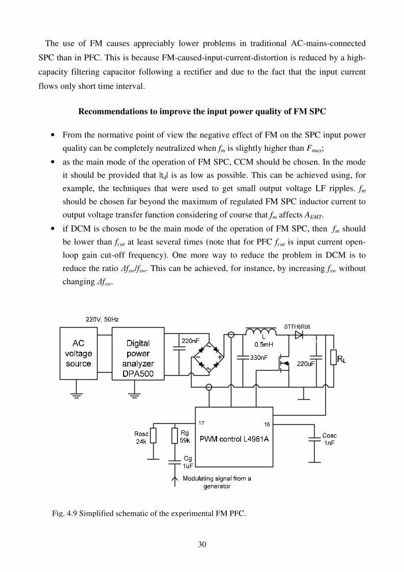
Fig. 4.9 Simplified schematic of the experimental FM PFC.
The use of FM causes appreciably lower problems in traditional AC-mains-connected
SPC than in PFC. This is because FM-caused-input-current-distortion is reduced by a high-
capacity filtering capacitor following a rectifier and due to the fact that the input current
flows only short time interval.
Recommendations to improve the input power quality of FM SPC
• From the normative point of view the negative effect of FM on the SPC input power
quality can be completely neutralized when fm is slightly higher than Fmax;
• as the main mode of the operation of FM SPC, CCM should be chosen. In the mode
it should be provided that |td| is as low as possible. This can be achieved using, for
example, the techniques that were used to get small output voltage LF ripples. fm
should be chosen far beyond the maximum of regulated FM SPC inductor current to
output voltage transfer function considering of course that fm affects AEMT.
• if DCM is chosen to be the main mode of the operation of FM SPC, then fm should
be lower than fcut at least several times (note that for PFC fcut is input current open-
loop gain cut-off frequency). One more way to reduce the problem in DCM is to
reduce the ratio ∆fsw/fsw. This can be achieved, for instance, by increasing fsw without
changing ∆fsw.

31
The recommendations proposed for improving the input power quality in CCM also have
been verified experimentally using 360W FM PFC shown in Fig. 4.9. PF and the input
current THD were measured using the power analyzer DPA500. Table 4.1 presents
measured THD and PF for different ∆fsw, fm and output power Pout=360W (nominal) and
Pout=102W.
Table 4.1
Measured PF and input current THD for unmodulated and FM PFC.
∆fsw, kHz fm, kHz Pout=102W Pout=360W
JK THD, % JK THD, %
unmodulated 0.983 9.8 0.993 6.45
10 1 0.983 9.8 0.993 6.45
20 1 0.981 9.9 0.992 6.5
30 1 0.982 9.85 0.992 6.5
40 1 0.981 9.95 0.991 6.6
10 5 0.983 9.8 0.993 6.45
20 5 0.983 9.8 0.993 6.45
30 5 0.983 9.8 0.993 6.45
40 5 0.982 9.8 0.993 6.45
The results obtained show that the input power quality does not worsen for fm=5kHz and
different ∆fsw using FM even with high ∆fsw. However when fm=1kHz then THD increases
slightly. This can be explained by the fact that when fm=5kHz, the frequencies of the LF
components caused by FM are beyond the power analyzer measurement range (note that
DPA500 maximum analysis frequency is Fmax=3kHz). That is why the negative effect of
FM on PFC input power quality from the normative point of view can be completely
neutralized. Meanwhile when fm=1kHz, increase in THD is negligible, because the
recommendations proposed are considered as follows: firstly, fm at least several times lower
than input current open loop gain cut-off frequency (for this PFC fcut=10kHz), and secondly,
the artificial delay circuit proposed in the doctoral thesis was used to get small td in CCM. It
can be concluded that the experimental results confirm that the recommendations proposed
can be very effective to eliminate the negative effect of FM on PFC input power quality.

32
CONCLUSIONS
It can be concluded from the results obtained that FM as one of the spread spectrum
techniques is very effective solution to reduce EMI because the main characteristics of SPC
such as the output voltage ripples, the efficiency and the input power quality (mainly power
factor and THD) are not virtually affected due to FM, if the recommendations proposed in
the doctoral thesis are considered. The results obtained in the research also show that the use
of FM has to play a large role in reducing EMI of SPC. This is because apart from its
advantages it has also relatively smaller drawbacks, than the other EMI suppression
techniques because, firstly, FM is sufficiently easy to implement and it practically do not
increase the size and cost of SPC (especially if it is implemented on a PWM integrated
circuit), secondly, it has relatively small negative effects on important SPC quality
characteristics and sometimes the adverse effects can be even neutralized completely (e.g. it
is proved in the thesis that from the normative point of view the negative effect of FM can
be completely neutralized when fm is slightly higher than maximum power analyzer
frequency Fmax).
The effectiveness of the use of FM mainly defined by the first harmonic attenuation,
depends not only on modulating signal parameters (as it was assumed in the majority of
publications analyzed) but also on the switching frequency fsw and power stage parameters.
The attenuation can be appreciably improved by properly choosing fsw or using the
optimized double-slope modulating waveform for which optimal parameter t0 value is to be
found using the procedure developed in the doctoral thesis.
The LF ripples that have been considered as the main problem of the use of FM, in
principle are not significant problem as it also is proved in the thesis. For example, the LF
ripples can be significantly mitigated in CCM by reducing the difference between the
switching delays which is the main cause of the problem. This can be achieved, for
example, by using proposed artificial delay circuit to get small td. The LF ripples in DCM
can be reduced only if fm is lower than fcut at least several times or by lowering the ratio
∆fsw/fsw. From the HF switching ripples point of view the boost or related topologies should
be used for FM SPC.
The input current LF components caused by FM are responsible for worsening the input
power quality. The causes of the problems are the same as for the output voltage LF ripples.

33
The input power quality of FM SPC can be appreciably improved taking in account the
similar recommendations as for reducing the LF output voltage ripples.
The results obtained in the thesis also show that for higher fsw, the negative effect of FM
on the output voltage ripples and the input power quality is lower. In fact, this coincides
with the modern SPC development trend to increase SPC switching frequencies.
The results presented and the calculation procedures developed could be used for
designing and developing high-quality FM SPC. In general, we can conclude that FM is
very effective solution to reduce EMI in SPC with small negative effect on FM SPC main
quality characteristics if the results and the recommendations proposed are considered.
34
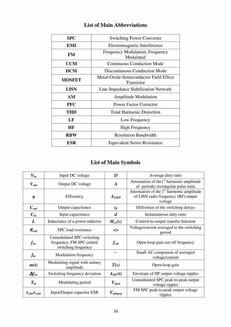
List of Main Abbreviations
SPC Switching Power Converter
EMI Electromagnetic Interference
FM Frequency Modulation; Frequency
Modulated
CCM Continuous Conduction Mode
DCM Discontinuous Conduction Mode
MOSFET Metal-Oxide-Semiconductor Field Effect
Transistor
LISN Line Impedance Stabilization Network
AM Amplitude Modulation
PFC Power Factor Corrector
THD Total Harmonic Distortion
LF Low Frequency
HF High Frequency
RBW Resolution Bandwidth
ESR Equivalent Series Resistance
List of Main Symbols
Vin Input DC voltage D Average duty ratio
Vout Output DC voltage A Attenuation of the1
st harmonic amplitude
of periodic rectangular pulse train
η Efficiency AEMT
Attenuation of the 1st harmonic amplitude
of LISN radio frequency (RF) output
voltage
Cout Output capacitance td Difference of the switching delays
Cin Input capacitance d Instantaneous duty ratio
L Inductance of a power inductor Hco(s) Control-to-output transfer function
Rout SPC load resistance <> Voltage/current averaged to the switching
period
fsw
Unmodulated SPC switching
frequency; FM SPC central
switching frequency fcut Open-loop gain cut-off frequency
fm Modulation frequency Small AC component of averaged
voltage/current
m(t) Modulating signal with unitary
amplitude T(s) Open-loop gain
∆fsw Switching frequency deviation AHF(t) Envelope of HF output voltage ripples
Tm Modulating period Vop-p Unmodulated SPC peak-to-peak output
voltage ripples
rcin,rcout Input/Output capacitor ESR Vofmp-p FM SPC peak-to-peak output voltage
ripples

35
REFERENCES
1. Rashid M.H. Power Electronics Handbook. – New York: Academic Press, 2001. –895 p.
2. Tse. C.K. Complex Behavior of Switching Power Converters. – New York: CRC Press
LCC, 2004. – 262 p.
3. Erickson R.W. Fundamentals of Power Electronics. – New York: Kluwer Academic
Publishers, 1997. – 791. p.
4. Mammano B. and Carsten B. Understanding and optimizing electromagnetic compatibility
in switchmode power supplies // Proceedings of Unitrode (TI) Power Supply Design
Seminar Topics, 2002, SEM1500.
5. Tse K.K., Chung H.S., Hui S.Y., So H.C. An Evaluation of the Spectral Characteristics of
Switching Converters with Chaotic Carrier-Frequency Modulation // IEEE Transactions on
Industrial Electronics. – 2003. - Vol.50, No.1. - pp. 171-181.
6. Gonzalez D., Balcells J., Santolaria A., Bunetel J., Gago J., Magnon D., Brehaut S.
Conducted EMI Reduction in Power Converters by Means of Periodic Switching Frequency
Modulation // IEEE Transactions on Power Electronics. – 2007. - Vol.22, No.6. - pp. 2271-
2281.
7. Wang S., Lee F. C., Odendaal W. G. Improving the performance of boost PFC EMI filters //
Proceedings of IEEE Applied Power Electronics Conference and Exposition, Feb. 2003. -
pp. 368–374.
8. H. Li, Z. Li, B. Zhang, K. Tang, W. Halang. Suppressing electromagnetic interference in
direct current converters // IEEE Circuits and Systems Magazine, no.4. – 2009.– pp.10-28.
9. K. Mainali, R. Oruganti. Conducted EMI Mitigation Techniques for Switch-Mode Power
Converters: A Survey // IEEE Transactions on Power Electronics. – 2010. - Vol. 25, No.9. -
pp. 2344 - 2356.
10. Ott H.W. Electromagnetic Compatibility Engineering. – New York: J. Wiley&Sons, 2009. –
845 p.
11. Tse K., Chung H., Hui S., So H. Comparative Study of Carrier-Frequency Modulation
Techniques for Conducted EMI Suppression in PWM Converters // IEEE Transactions on
Industrial Electronics. – 2002. - Vol. 49, No.3. - pp. 618-627.
12. Kuisma M. Variable Frequency Switching in Power Supply EMI-control: An Overview.
IEEE Aerospace and Electronic Systems Magazine. - Vol. 18, No 12. - Dec. 2003. – pp.18 -
22.
36
13. Hardin K.B., Fessler J.T., Bush D.R. Spread Spectrum Clock Generation for the Reduction
of Radiated Emissions // Proceedings of IEEE International Symposium on Electromagnetic
Compatibility. - August 1994. – pp. 227-231.
14. Skinner H., Slattery K. Why spread spectrum clocking of computing devices is not cheating
// IEEE International Symposium on Electromagnetic Compatibility, 2001. – pp. 537 - 540.
15. Lin F., Chen D.Y. Reduction of Power Supply EMI Emission by Switching Frequency
Modulation // IEEE Trans. On Power Electronics. – 1994. – Vol.9, No.1. – pp.132-137.
16. Kuisma M., Jarvelainen T., Silventoinen P. Analyzing Voltage Ripple in Variable
Frequency DC/DC Boost Converter // IEEE 2004 Power Electronics Specialists conference.
– 2004. - pp. 1085-1089.
17. Stepins D. Examination of influence of periodic switching frequency modulation in dc/dc
converters on power quality on a load // Proceedings of the 11th Biennial Baltic Electronics
Conference, Tallinn, Estonia, Oct. 6-8, 2008. – pp. 285-288.
18. Balcells J., Gonzales D., Gago J., Satolaria A., Bunetel J.C.L., Magnon D., Brehaut S.
Frequency modulation techniques for EMI reduction in SMPS // Proceedings of the 9th
European Conference on Power Electronics and Applications, EPE’05. – 2005. – P. 1 – 6.
19. Gosavi A. Application of Spread Spectrum technique for EMI reduction in boost converter -
A case study // Proceedings of 10th International Conference on Electromagnetic
Interference & Compatibility (INCEMIC 2008). - 2008. – P. 145-148.
20. Jankovskis J., Stepins D., Pikulins D. Improving effectiveness of the use of frequency
modulation in power converters // Proceedings of the 12th Biennial Baltic Electronics
Conference, Tallinn, Estonia, Oct. 4-6, 2010. – pp. 327-330.
21. Jankovskis J., Stepins D., Pikulins D. Lowering of EMI Noise in Boost Type PFC by the use
of Spread Spectrum // Electronics and Electrical Engineering. - 6 (94). – 2009. – pp. 15.-18.
22. J.-C. Bunetel, D. Gonzalez, J. Balcell. Impact of periodic switching frequency modulation
control to reduce conducted EMI in power factor converters // 32nd Annual Conference of
IEEE Industrial Electronics Society (IECON2006), Paris, France, Nov. 7-10, 2006. – pp.
2541-2545.
23. Johnson S. and Zane R. Custom spectral shaping for EMI reduction in high-frequency
inverters and ballasts // IEEE Transactions on Power Electronics. - vol. 20. - November
2005. - pp. 1499 – 1505.
24. Barragan, L., Navarro, D., Acero, J., Urriza, I. and Burdío, J-M. FPGA Implementation of a
Switching Frequency Modulation Circuit for EMI Reduction in Resonant Inverters for

37
Induction Heating Appliances // IEEE Transactions on Industrial Electronics. - vol. 55. -
January 2008. - pp. 11 – 20.
25. Mei-Ling Yeh, Wan-Rone Liou, Hsiang-Po Hsieh, Yu-Jei Lin. An Electromagnetic
Interference (EMI) Reduced High-Efficiency Switching Power Amplifier // IEEE
Transactions on Power Electronics. – 2010. - Vol.25, No.3. - pp. 710-718.
26. Mainali K., Oruganti R. Simple analytical models to predict conducted EMI noise in a
power electronic converter // Proceedings of IEEE Industrial Electronics Society
Conference, 2007. - pp. 1930–1936.
27. Santolaria A. Effects of Switching Frequency Modulation on the Power Converter’s Output
Voltage // IEEE Transactions on Industrial Electronics. – 2009. - Vol.56, No.7. - pp. 2729-
2737.
28. Kultgen M.A. Spread spectrum modulation of a clock signal for reduction of
electromagnetic interference // U.S. Patent 7417509, August, 26 2008.
29. Stepins D. Analysis of Output Voltage of Switching Frequency Modulated DC-DC
Converter Operating in Discontinuous Conduction Mode // Proceedings of IEEE
International Symposium on Industrial Electronics (IEEE ISIE10), Bari, Italy, July 4-7,
2010. – pp. 670-675.
30. Stepins D. Examination of Power Converters with Modulated Switching Frequency //
Electronics and Electrical Engineering. - 9(105). – 2010. - pp. 33.-38.
31. Mihalic F., Milanovic M. EMI reduction in randomized boost rectifier // Proceedings of
IEEE International Symposium on Industrial Electronics (ISIE’99), Bled, Slovenia, 1999. -
pp. 457-462.
32. Jankovskis J., Stepins D., Pikuļins D. Efficiency of PFC Operating in Spread Spectrum
Mode for EMI Reduction // Electronics and Electrical Engineering. - 7.– 2010.–pp.13.-16.
33. Beķeris E. Signālu Teorijas Elementi 1. daļa. – Rīga: Zinātne, 1998. – 198. lpp.
34. A. van den Bossche, V.Valchev, Inductors and Transformers for Power Electronics, 1st ed.,
Taylor and Francis, 2005. – 447p.
35. Musznicki P., Schanen JL., Granjon P., Chrzan P.J. Better understanding EMI generation of
power converters // Proceedings of IEEE Power Electronics Specialists Conference
(PESC2005), Recife, Brazil, June 2005. – pp. 1052-1056.


