STUDY OF NANOSCALE MATERIALS USING POSITRON ANNIHILATION SPECTROSCOPY By PRIYA MAHESHWARI CHEM01200904007 Bhabha Atomic Research Centre, Mumbai A thesis submitted to the Board of Studies in Chemical Sciences In partial fulfillment of requirements For the Degree of DOCTOR OF PHILOSOPHY of HOMI BHABHA NATIONAL INSTITUTE AUGUST, 2013
Transcript
STUDY OF NANOSCALE MATERIALS USING POSITRON ANNIHILATION
SPECTROSCOPY
By
PRIYA MAHESHWARI CHEM01200904007
Bhabha Atomic Research Centre, Mumbai
A thesis submitted to the
Board of Studies in Chemical Sciences
In partial fulfillment of requirements
For the Degree of
DOCTOR OF PHILOSOPHY
of
HOMI BHABHA NATIONAL INSTITUTE
AAUUGGUUSSTT,, 22001133
HOMI BHABHA NATIONAL INSTITUTE
Recommendations of the Viva Voce Board
As members of the Viva Voce Board, we certify that we have read the dissertation
prepared by Priya Maheshwari entitled “Study of Nanoscale materials Using
Positron Annihilation Spectroscopy” and recommend that it may be accepted as
fulfilling the dissertation requirement for the Degree of Doctor of Philosophy.
Date:
Chairman: Prof. A. Goswami
Date:
Guide: Prof. P. K. Pujari
Date:
Member 1: Prof. G. Amarendra
Date:
Member 2: Prof. B. S. Tomar
Date:
Member 3: Prof. S. Kapoor
Final approval and acceptance of this dissertation is contingent upon the candidate’s
submission of the final copies of the dissertation to HBNI.
I hereby certify that I have read this dissertation prepared under my direction and
recommend that it may be accepted as fulfilling the dissertation requirement.
Date:
Place:
STATEMENT BY AUTHOR
This dissertation has been submitted in partial fulfillment of requirements for an advanced
degree at Homi Bhabha National Institute (HBNI) and is deposited in the Library to be
made available to borrowers under rules of the HBNI.
Brief quotations from this dissertation are allowable without special permission, provided
that accurate acknowledgement of source is made. Requests for permission for extended
quotation from or reproduction of this manuscript in whole or in part may be granted by
the Competent Authority of HBNI when in his or her judgment the proposed use of the
material is in the interests of scholarship. In all other instances, however, permission must
be obtained from the author.
Priya Maheshwari
DECLARATION
I, hereby declare that the investigation presented in the thesis has been carried out by me. The
work is original and has not been submitted earlier as a whole or in part for a degree /diploma
at this or any other Institution / University.
Priya Maheshwari
Dedicated to …..
My Grandparents &
Parents
List of Publications
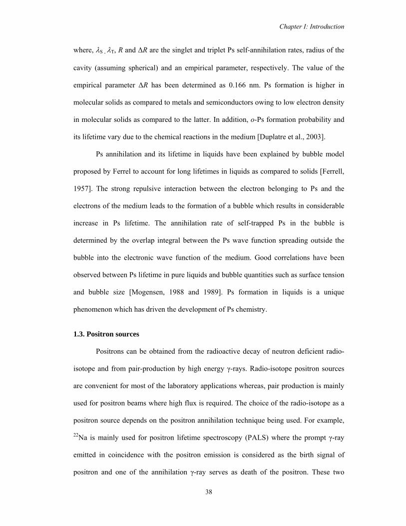
REFFEREED JOURNALS 1. Study of iron phthalocyanine organic semiconductor thin films using slow positron
beam
P. Maheshwari, D. Dutta, S. Samanta, A. Singh, D. K. Aswal, A. V. R. Reddy and P.
K. Pujari
Phys. Stat. solidi c 6,11, (2009) 2589-2591.
2. Microstructure study of supported liquid membranes using slow positron beam
P. K. Pujari, P. Maheshwari, S. K. Sharma, D. Dutta, K. Sudarshan and A. V. R.
Reddy
Phys. Stat. solidi c 6,11, (2009)2417-2419.
3. Effect of interfacial hydrogen bonding on the freezing/melting behavior of nano-
confined liquids
P. Maheshwari, D. Dutta, S. K. Sharma, K. Sudarshan, P. K. Pujari, M. Majumdar,
B. Pahari, B. Bandyopadhyay, K. Ghosharay and A. Ghosharay
J. Phys. Chem. C,114 (2010) 4966.
4. Study of interfaces in organic semiconductor heterojunctions
P. Maheshwari, D. Dutta, K. Sudarshan, S. K. Sharma, S. Samanta, A. Singh, D. K.
Aswal and P. K. Pujari,
Journal of Physics: Conference Series 262 (2011) 012036.
5. Defect depth profiling in organic semiconductor multilayers
Priya Maheshwari, P. K. Pujari, S. K. Sharma, K. Sudarshan, D. Dutta, S. Samanta,
A. Singh, D. K. Aswal, R. Ajay Kumar and I. Samajdar
Organic Electronics, 13 (2012)1409.
6. Phase transition of water confined in Saponites using Positron annihilation
spectroscopy
Priya Maheshwari, S. K. Sharma, D. Dutta, K. Sudarshan, P. K. Pujari
Mat. Sci. Forum, 733 (2013) 111.
7. Phase transition of nanoconfined water in clay: Positron annihilation, Nuclear
magnetic resonance and Dielectric relaxation studies
Priya Maheshwari, P. K. Pujari, S. K. Sharma, D. Dutta, K. Sudarshan, V. S. Mithu,
P. K. Madhu, S. K. Deshpande, P. N. Patil and N. Raje
J. Phys. Chem. C, 117 (2013) 14313.
8. Depth dependent inhomogeneities in nanoscale OSC films: PAS and XRR study
Priya Maheshwari, D. Bhattacharya, S. K. Sharma, S. Mukherjee, S. Basu and P. K.
Pujari
(Communicated)
9. Direct evidence of linkage between pore interconnectivity and permeability of metal
ions in PTFE supported liquid membranes: A slow positron beam study
Priya Maheshwari, D. Dutta, K. Sudarshan, S. K. Sharma, P. K. Mohapatra, P. U.
Sastry and P. K. Pujari
(Communicated)
SYMPOSIUM
1. Study of pore architecture in track etched polycarbonate membranes using slow
positron beam
P. Maheshwari, S. K. Sharma, D. Dutta, K. Sudarshan, and P. K. Pujari
Proceedings of Nuclear and Radiochemistry symposium (NUCAR)- 2011.
2. Study of phase transition of 2D confined water
Priya Maheshwari, S. K. Sharma, D. Dutta, K. Sudarshan, P. N. Patil and P. K. Pujari
Proceedings of Nuclear and Radiochemistry symposium (NUCAR)- 2013.
ACKNOWLEDGEMENTS
This thesis would not have been possible without the support and encouragement of many
people who contributed and extended their valuable assistance in the completion of the
research work. I feel short of words in expressing my appreciation for their help at
various stages of this work.
First and foremost, I would like to express my sincere gratitude to my thesis advisor Prof.
P. K. Pujari for his continuous support to my work, his patience, encouragement,
enthusiasm and immense knowledge. His intellectual ideas and guidance helped me in my
research work and writing this thesis. He has always been a source of motivation for me
in difficult times in research or otherwise. I express my deep sense of appreciation for his
support and for energizing me to overcome all the hurdles.
Besides my advisor, I would like to thank members of my doctoral committee; Prof. A.
Goswami, Prof. B. S. Tomar, Prof. G. Amarendra and Prof. S. Kapoor for their
encouragement, insightful comments and fruitful ideas during the course of the thesis
work which have been useful for the progress of the work. I would like to express my
gratitude to Dr. D. Dutta, Dr. K. Sudarshan and Dr. S. K. Sharma for helping me in
learning the instrumentation and experimental techniques. I share the credit of my work
with them for helping me in carrying out the experiments round the clock and sharing the
ideas. I would also like to thank my lab mates Dr. S. Mukherjee and Dr. P. N. Patil for
their timely help.
I cannot find words to express my gratitude to Dr. Suparna Sodaye who has been there all
the times to encourage and motivate me to work cheerfully. Her constant support and
presence have been an emotional support for me to overcome all the hurdles on my path. I
would also like to thank my senior colleagues Dr. R. Acharya and Dr. Rahul Tripathi for
their encouragement and advice during the course of the research work. I also owe a great
debt of gratitude to my collaborators Dr. S. K. Deshpande (UGC-CSIR, BARC), Dr. P. K.
Madhu (TIFR), Mr. V. S. Mitthu (TIFR), Dr. N. Raje (ACD, BARC), Dr. N. Padma
(TPD, BARC), Dr. D. Bhattacharya (SSPD, BARC), Dr. S. Basu (SSPD, BARC) and Dr.
D. K. Aswal (TPD, BARC) for their help and fruitful discussions during the course of the
work. My heartfelt appreciation goes to Dr. Soumen Samanta for his friendship and
constant support in carrying out work on organic semiconductor thin films.
Apart from the intellectual support, an emotional support is always needed to conquer the
hardships. For this, I would like to thank, from the bottom of my heart, my friends Alka,
Megha, Chun Mei, Sanhita, Manish, Gayatri, Divya and Kanishka for their warm
friendship.
Last but not the least, my deepest gratitude is to my family for their warm support which
brings belief and hope into my life; to my beloved parents, who have been so caring and
supportive of me all the time and my grandparents, who have always been a source of
inspiration towards achieving the goals in life. Immense love and affection of my sisters
and brothers have been invaluable in the journey towards my goal.
Apart from all the people mentioned in this acknowledgment, there are many others who
have helped me in various ways during the course of this thesis work. My sincere thanks
and apologies to all those I may have forgotten to mention.
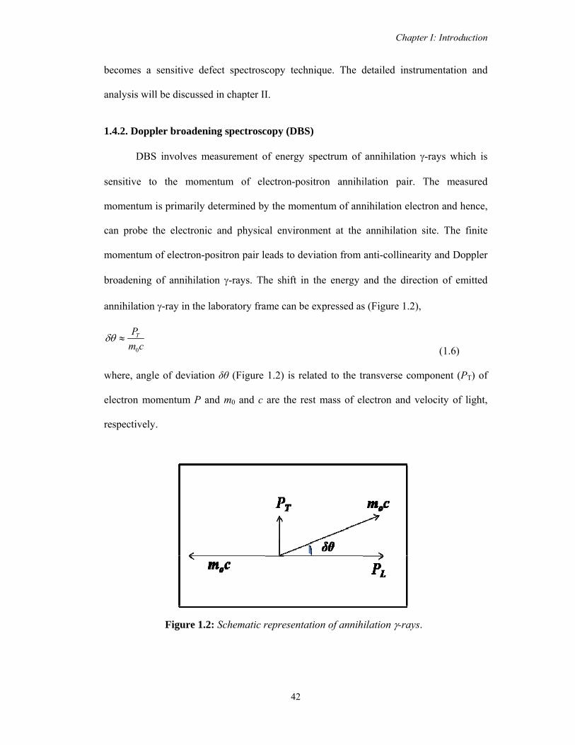
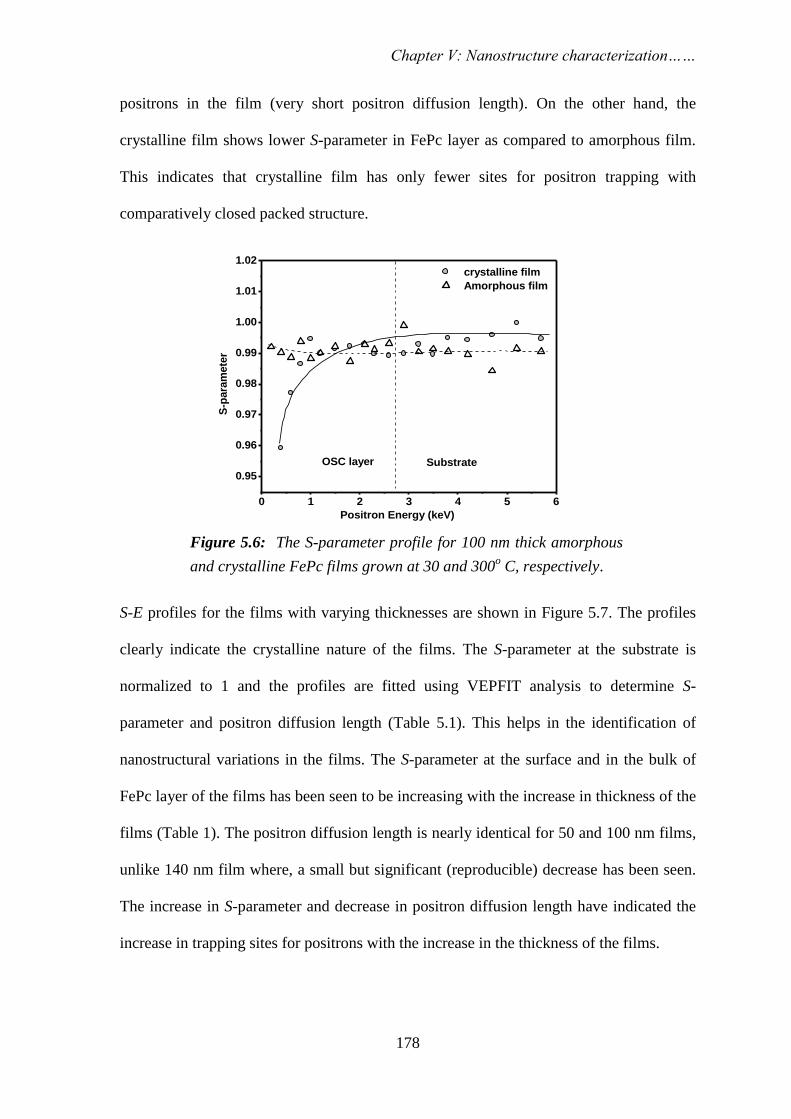
and desiccated to minimize purge effects. The samples were placed over ATR crystal and
maximum pressure was applied using the slip-clutch mechanism. All spectra were
collected at 4 cm-1 spectral resolution using sample and background collection time of
one minute each. FTIR data analysis was done using Opus (version 6.0) software from
Bruker.
3.2.4. Differential scanning calorimetry (DSC)
Water confined in saponite clay
DSC measurements in temperature modulated and unmodulated (conventional)
mode were carried out in temperature range from 298-198 K. The conventional scanning
was performed by METTLER TOLEDO Thermal Analysis system using argon gas (flow
rate 60 ml min-1) in the DSC cell purge. The scanning speed was fixed at 2.0 K min-1. The
temperature modulated measurements were carried out using METTLER TOLEDO
Thermal Analysis system using argon gas (flow rate 60 ml min-1) in the DSC cell purge.
The system allows heating or cooling scans in the modulated DSC regime. The samples
were weighed and placed into standard Al sample pans with crimped lids. A matching
empty sample pan with crimped lid was used as the reference. The scanning was
performed by first cooling the samples from room temperature down to 198 K and then
starting the heating ramp to room temperature at a rate 2 K min-1. In order to obtain
Chapter III: Nanodroplets: Phase transitions…..
92
accurate and reproducible results, three experimental parameters, underlying heating rate,
modulation amplitude and modulation period were carefully selected. The modulation
period was varied from minimum value of 15 seconds to maximum value of 30 seconds
with modulation amplitudes of 1 K (+/- 0.5 K).
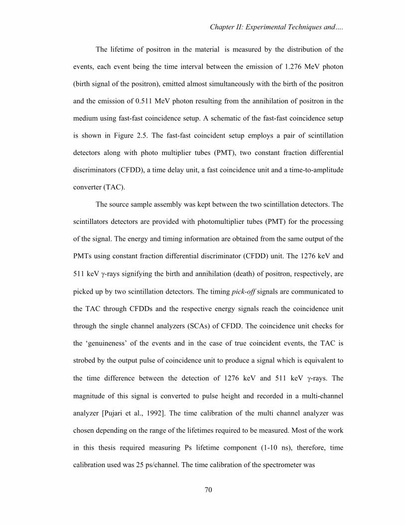
3.2.5. Positron annihilation spectroscopy
3.2.5a. Ethylene glycol and isopropanol
Temperature dependent positron lifetime and Doppler broadening measurements
were carried out in the temperature range from room temperature to 245 K in the case of
ethylene glycol and from 210 to 170 K in the case of isopropanol, in both cooling and
heating cycle. For low temperature measurements, the sample (powdered form and
hermetically sealed) along with the source (~8 μCi deposited on thin Kapton foil) was
mounted on the cold head of APD closed cycle helium refrigerator. Temperature variation
was carried out in 1 K interval with an accuracy of ±0.01 K. Doppler broadened
annihilation radiation measurements were carried out using an HPGe detector having
resolution of 1.8 keV at 1332 keV photo peak of 60Co. The shape parameter, namely, S-
parameter defined as the ratio of the number of counts falling in a fixed energy window
centered at 511 keV to the total number of counts, was evaluated. The experiments were
repeated in different samples (both cooling and heating cycle) and the reproducibility of
the data was seen to be good in both the liquids confined in zeolite. Positron annihilation
lifetime measurements were carried out using BaF2 scintillation detectors in a fast-fast
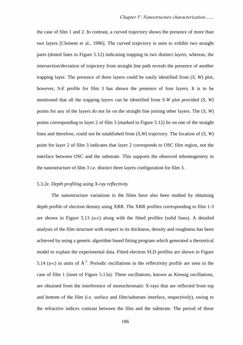
coincidence system. The time resolution measured with a 60Co source was 300 ps and the
time calibration was 25 ps per channel. Data analysis was carried out using PATFIT
program [Kirkegaard et al., 1981 and 1989; Kirkegaard and Eldrup, 1972].
Chapter III: Nanodroplets: Phase transitions…..
93
3.2.5b. Water confined in saponite clay
Low temperature positron lifetime and Doppler broadening measurements were
carried out in the same experimental set up (APD closed cycle helium refrigerator) and
the sample geometry as for ethylene glycol and isopropanol. The temperature variation
was carried out in the range of 200-300 K in both heating and cooling cycles. The
temperature variation was carried out in 2 K interval with an accuracy of ± 0.01 K.
Doppler broadened annihilation radiation measurements were carried out using an HPGe
detector having resolution of 2.2 keV at 1332 keV photo peak of 60Co and the variation of
S-parameter was measured. Positron annihilation lifetime measurements were carried out
using BaF2 scintillation detectors in a fast-fast coincidence system. The time resolution
measured with a 60Co source was 295 ps and the time calibration was 25 ps per channel.
Data analysis was carried out using PATFIT program.
3.2.6. Nuclear magnetic resonance
NMR measures the absorption of electromagnetic radiation during the transition
from spin states of atomic nuclei. In NMR experiments, a constant strong magnetic field
H leads to splitting of energy levels of the nuclei depending upon the spin states. The
energy difference between the two levels is given by,
πγ2hHE =Δ (3.1)
where, γ is a constant termed as gyromagnetic ratio of the nucleus defined as,
mq
2=γ (3.2)
where, q and m represent the electronic charge and mass of the nucleus, respectively. An
oscillating field B1 applied to the sample leads to absorption of energy, resulting in
excitation of the nuclei. The energy absorbed by a given nucleus, ∆E depends on the local
Chapter III: Nanodroplets: Phase transitions…..
94
magnetic field experienced by the nucleus. The local magnetic field is the resultant of
applied field and the field created by electron current in the molecular orbital. Therefore,
resonance frequency or ∆E depends on the electronic environment, and consequently on
the structural properties of the sample. The variation of interaction between the nuclei due
to any phase transition can be detected from the change in structural and dynamical
properties of the system which can be derived from chemical shift measurement and the
analysis of relaxation time.
3.2.6a. Chemical shift and relaxation time
The chemical shift (δ ) is defined as the variation of NMR resonance frequencies
of the same kind of nucleus, due to the variation of electronic distribution. It is measured
as the resonance frequency of the nucleus relative to a standard. The total magnetic field
experienced by a nucleus includes local magnetic field induced by the electronic currents
in the molecular orbitals which vary depending upon the local geometry (bond angle,
length, bonding partner etc.).
The radio frequency, RF (equal to the energy difference between the two levels)
applied to the sample causes spins to flip and redistribute among the two energy levels.
The energy absorbed by the nuclear spins induces a voltage that can be detected by a
suitably tuned coil of wire, amplified and the signal is displayed as free induction decay
(FID). The relaxation process eventually returns the spin system to thermal equilibrium,
which occurs in the absence of any perturbing RF pulses. The two relaxation processes
are; spin-lattice (or longitudinal relaxation time, T1) and spin-spin (or transverse
relaxation time, T2) relaxation. T1 measures how fast the magnetization relaxes back
along the z-axis, whereas, T2 measures how fast the spins exchange energy in the
transverse (xy) plane. There are several mechanisms by which molecular motions can
influence nuclear relaxation; direct interaction with the nearby nuclei (dipole-dipole),
Chapter III: Nanodroplets: Phase transitions…..
95
chemical shift effects, quadrupole interaction and j-j coupling. Different pulse sequences
are employed to measure relaxation times. Pulse sequence is the set of RF pulses applied
to the sample to produce a specific form of NMR signal.
In the present work, 90o FID pulse and spin-echo pulse sequences are used to
measure T2. In the 90o FID pulse sequence, net magnetization is rotated down into the xy
plane with a 90o pulse. The net magnetization vector begins to precess about z-axis. The
decay time is determined from the FID curve. The FID is an observable NMR signal
generated by non-equilibrium nuclear spin magnetization precessing about the magnetic
field direction. The non-equilibrium magnetization can be induced generally by applying
a pulse of resonance frequency (90o pulse as mentioned above) close to the Larmor
frequency of the nuclear spin. In the spin-echo pulse sequence, initial 90o pulse rotates
the magnetization into y-direction. Due to inhomogeneous magnetic field, spins fan out in
the xy plane with a loss of phase coherence. A 180o pulse applied after time τ, results in
phase coherence along the negative y-direction producing a signal called echo after time
2τ. Following the spin-echo, phase coherence will again be lost but can be regained with
another 180° pulse. T2 can be obtained from the amplitudes of the decaying echoes.
3.2.6b. Static and Magic angle spinning
NMR spectral lines obtained in static measurement from a liquid specimen are
much narrower than that in the solids. This difference in the behavior arises from the
static anisotropic interactions to which the nuclei are subjected in the solid state. By
contrast, in liquids the rapid isotropic motion of the nuclei average out the anisotropic
interactions and effectively remove them from the spectrum. These anisotropic
interactions include chemical shift anisotropy, dipolar coupling and quadrupole
interactions. The rotation/spinning of the solid specimen so as to mimic the rotation of
nuclei as in liquids can help in averaging out the anisotropic interactions in the solids.
Chapter III: Nanodroplets: Phase transitions…..
96
Rapid rotation about an axis inclined to an angle (magic angle) to the direction of
magnetic field can remove anisotropic part of chemical shift anisotropy and dipolar
coupling and a narrower spectrum can be obtained.
In a strong magnetic field, the dipolar coupling between the nuclei depends on the
orientation of internuclear vector with the applied magnetic field, given as,
)1cos3( 2 −∝ θD (3.3)
where, θ is the angle between the internuclear vector and the direction of applied
magnetic field and D is the dipolar coupling constant which tends to zero at θ = 54.7o
known as the magic angle. In the magic angle spinning measurement, specimen is
spinned at an angle of 54.7o with respect to field direction. In the present work, magic
angle spinning (MAS) has been used in the case of water confined in saponite clay. The
effect of MAS on improving spectral resolution is evident from the Figure 3.2.
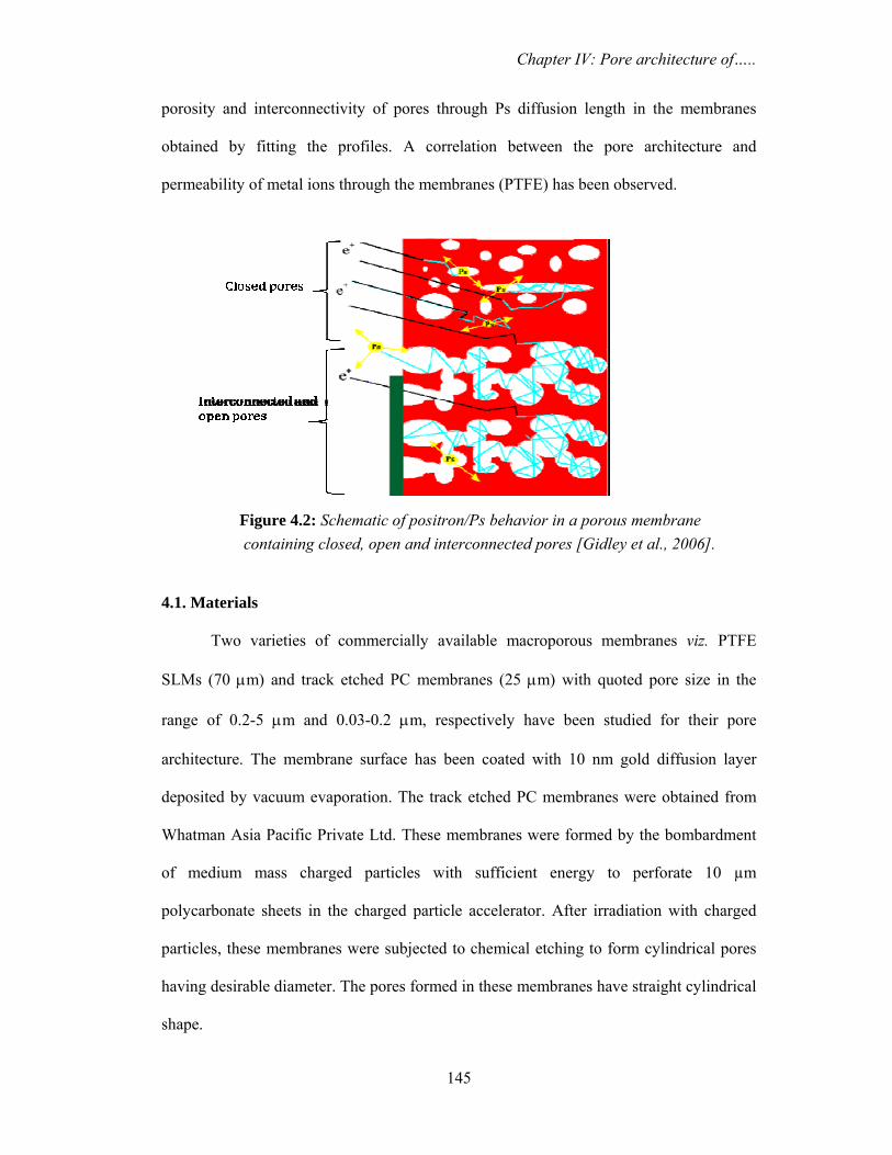
Figure 3.2: One-Dimensional 1H spectrum of water confined inside clay nanopores, when the sample is static (grey) and spinning at 5 kHz at magic angle (black) inside the 700 MHz NMR spectrometer. The peak at 0 ppm in MAS spectrum corresponds to Si-OH group in the clay platelets. Peaks with stars on top of them are MAS side bands of the water and Si-OH peaks.
Chapter III: Nanodroplets: Phase transitions…..
97
3.2.6c. Ethylene glycol and isopropanol
1H NMR studies were carried out at a resonance frequency of 42.53 MHz with a
Bruker MSL100 NMR spectrometer and at 9.97 kOe using a field-dial controlled Varian
V7400 electromagnet. All the samples were sealed under argon atmosphere in glass tubes.
A Bruker temperature controller was used to vary the sample temperature. The spin-spin
relaxation time (T2) has been measured by Hahn-echo method using the pulse sequence
90°-τ-180° signal acquisition, which eliminates the effect of magnetic field
inhomogeneity on T2 decay. 90° pulse length was set at 2.1 μs and τ values were varied
between 0.5 – 30 ms. The intensity of the resonance spectrum for a particular component
of the fluid in which the nuclear spins experience a certain kind of interaction, is given
by,
( ) ( ) ( ) .2exp2
2
im
iTiIiI ⎟⎟
⎠
⎞⎜⎜⎝
⎛−=
ττ
(3.4)
where I2τ(i) is the intensity corresponding to the ith component of the resonance spectrum
after a time 2τ after 90° pulse, and mi is 1 for exponential and 2 for Gaussian decay. I(i)
are the fractional intensities of the components having spin-spin relaxation times T2(i).
The total intensity of the spectrum is given by,
( ) ( )∑=i
total iII ττ 22. (3.5)
T2 decay curves for ethylene glycol was decomposed into two distinct Gaussian decays
whereas, three Lorentzian decay curves were employed to decompose T2 decay curve in
the case of isopropanol.
3.2.6d. Water confined in saponite clay
Solid-state 1H NMR measurements were performed at a magnetic field of 16.43 T
(700 MHz of 1H Larmor frequency) using Bruker AVIII NMR spectrometer. 4 mm triple-
Chapter III: Nanodroplets: Phase transitions…..
98
resonance probe was used for static and MAS experiments. Clay samples in the form of
fine powder were packed in 4 mm rotors using ceramic caps to perform low temperature
studies. All chemical shifts were referenced with respect to 1H chemical shift of Si–OH
groups in clay fixed to 0 ppm at 298 K. Chemical shift of 79Br in KBr sample was used
for temperature calibration in static as well as spinning samples. The transverse spin-spin
relaxation time T2* (T2′) was measured in the temperature range 325-240 K. T2
* values
were calculated by measuring the full width at half maximum of water peak obtained
from 1D spectrum of static and spinning clay sample obtained with just a 90˚ pulse. T2′
measurements were carried out by monitoring peak height in 1D 1H spectrum of clay
recorded after a spin-echo. The observed 1H peak height was plotted as a function of spin-
echo duration to obtain transverse dephasing curves. These curves were then fitted to a
single-exponential decay function to obtain transverse dephasing times (T2′ values).
3.2.7. Dielectric relaxation spectroscopy
In dielectric relaxation experiments collective polarization of all the polar
molecules in the sample is measured. The dielectric relaxation time provides the measure
of the time taken by a system to reach the final polarization after an electric field is
switched on (or off). The technique measures the dielectric response i.e. complex
dielectric function ε*(ω) of the system under study. The complex dielectric function,
ε*(ω) can be decomposed into real and the imaginary parts as,
)()()( '''* ωεωεωε −= (3.6)
The real ε′(ω) and imaginary ε″(ω) parts represent the storage and loss part, respectively
for a relaxation process. Different molecular theories of dielectric relaxation process
provide microscopic understanding of the relaxation phenomena existing in the system.
The dependence of ε*(ω) on angular frequency originates from different factors, (i)
Chapter III: Nanodroplets: Phase transitions…..
99
microscopic fluctuations of molecular dipoles, (ii) the propagation of mobile charge
carriers (translational diffusion of electron, holes or ions), and (iii) the separation of
charges at the interfaces which give rise to additional polarization. The sensitivity of
dielectric relaxation to intermolecular interactions and its ability to monitor cooperative
processes at molecular level help in the investigation of properties of individual
constituents of the system and hence, derivation of macroscopic bulk properties.
3.2.7a. The dielectric constant and polarization
The static dielectric constant (relative permittivity) of a material is given by,
oCC
=ε (3.7)
where, C is the capacitance of a parallel plate capacitor with the space between the plate
filled with a dielectric material and Co is the capacitance with vacuum in between the
plates. The permittivity of the material depends on the polarisability of the molecules in
between the plate. The polarization of the medium is a function of frequency of the
applied electric field and is defined as,
EP o )1( −= εε (3.8)
where, εo is the dielectric permittivity of vacuum and is equal to 8.854×10⁻¹² Fm-1 and E is
the applied electric field. The total polarizability is the sum of electronic, atomic and
orientation (in case of polar medium) polarization. The applied field leads to polarization
of the medium by displacing the charge distribution/aligning the dipoles in a direction
parallel to the field. Each of these mechanisms has a characteristic resonant or relaxation
frequency.
3.2.7b. Relaxation Times
Chapter III: Nanodroplets: Phase transitions…..
100
Dielectric relaxation is a consequence of the movement of dipoles or electric
charges due to the changing electric field. Dielectric relaxation processes lie in a wide
range of characteristic times, 105-10-12 s and is denoted by,
max21
πντ = (3.9)
where, τ is the characteristic relaxation time and νmax is the resonance frequency of the
relaxation process. Relaxation processes are characterized by a peak in the imaginary part
(ε″) and a step-like decrease of the real part (ε′) of the dielectric function. The relaxation
processes are usually analyzed by using model functions. In the present work, a general
model function introduced by Havriliak and Negami (H-N function) [Havriliak and
Negami, 1966 & 1967], has been used to analyze the dielectric response of the system
under study. The H-N function is defined as,
( )( )[ ] ⎥
⎥⎦
⎤
⎢⎢⎣
⎡
+
Δ+= −
βαωτ
εωεσ
ωεi
n
o
DC
1Im" (3.10)
where, ω = 2πf, Δε = εS-ε∞, where, εS and ε∞ are static and high frequency limiting values
of the dielectric constant, respectively, σDC is the conductivity contribution, τ is the
relaxation time and n, α and β are empirical exponents with values between 0 and 1.
3.2.7c. Instrumentation and measurement technique
Using a sinusoidal electric field, E*=Eo exp(iωt) with angular frequency ω and at
field strength within the linear response (for most materials Eo ≤ 106 Vs-1), the dielectric
function is derived by measuring the complex impedance Z*(ω) of the sample, defined as,
oo CZiEij
)(1
)()(
**
**
ωωωωεωε == (3.11)
Chapter III: Nanodroplets: Phase transitions…..
101
where, j*(ω) is the complex current density. Fourier correlation analysis in combination
with impedance analysis has been used to evaluate amplitude and the phase of Z*(ω). The
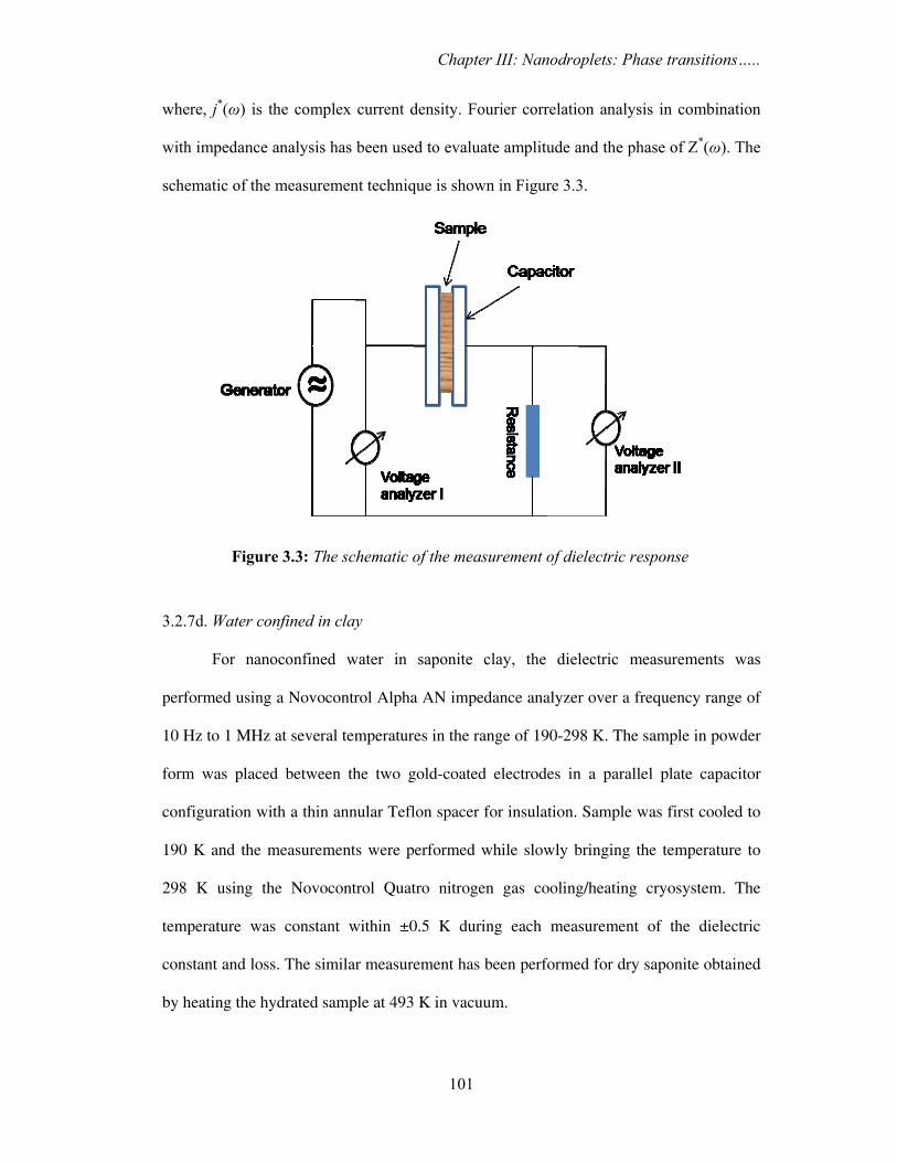
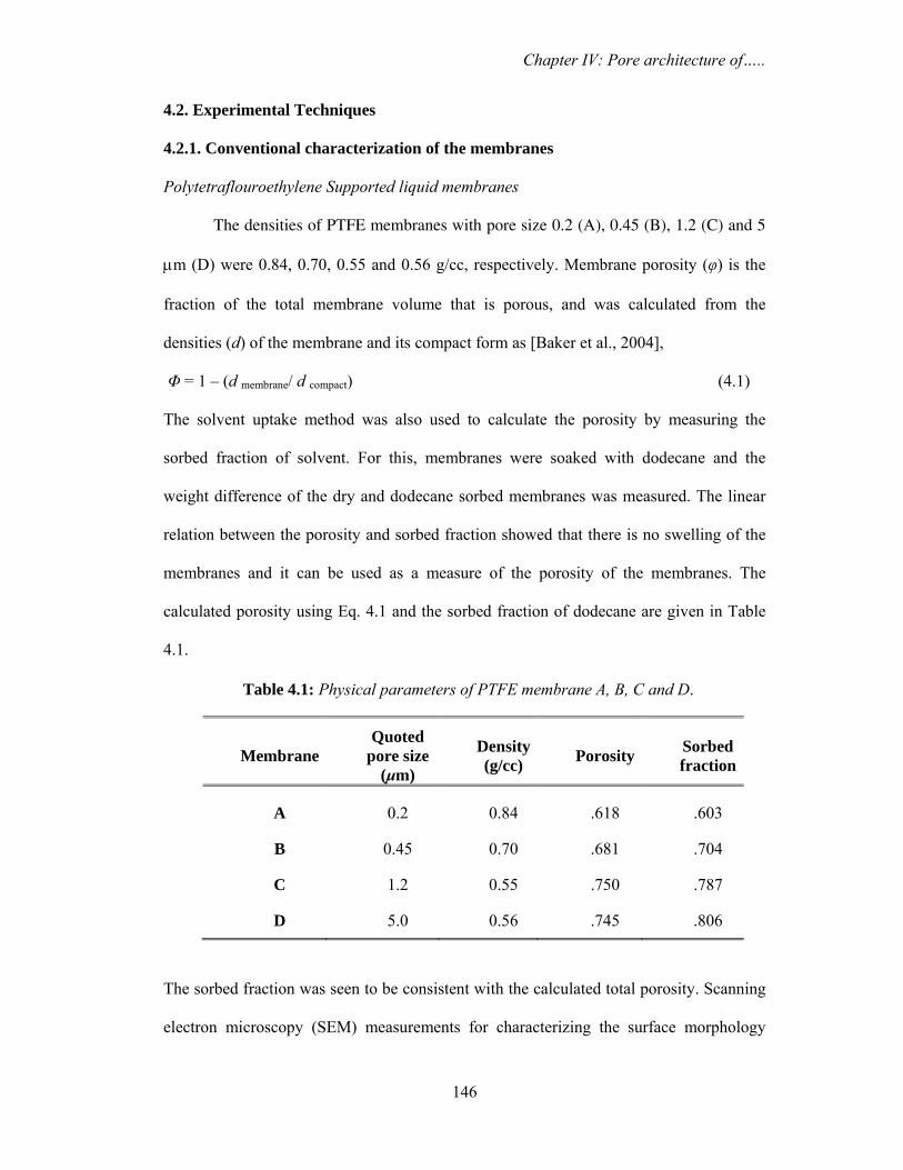
schematic of the measurement technique is shown in Figure 3.3.
3.2.7d. Water confined in clay
For nanoconfined water in saponite clay, the dielectric measurements was
performed using a Novocontrol Alpha AN impedance analyzer over a frequency range of
10 Hz to 1 MHz at several temperatures in the range of 190-298 K. The sample in powder
form was placed between the two gold-coated electrodes in a parallel plate capacitor
configuration with a thin annular Teflon spacer for insulation. Sample was first cooled to
190 K and the measurements were performed while slowly bringing the temperature to
298 K using the Novocontrol Quatro nitrogen gas cooling/heating cryosystem. The
temperature was constant within ±0.5 K during each measurement of the dielectric
constant and loss. The similar measurement has been performed for dry saponite obtained
by heating the hydrated sample at 493 K in vacuum.
Figure 3.3: The schematic of the measurement of dielectric response
Chapter III: Nanodroplets: Phase transitions…..
102
I. Freezing/melting behavior of ethylene
glycol and isopropanol confined in ZSM 5
Chapter III: Nanodroplets: Phase transitions…..
103
3.3. Results and Discussion
3.3.1. Ethylene glycol and isopropanol confined in ZSM 5
3.3.1a. PAS results
The change in positron/Ps annihilation parameters (S-parameter, o-Ps pick-off
lifetime and intensity) as a function of temperature is indicative of phase transition. In the
present case, S-parameter, o-Ps pick-off lifetime (τp) and intensity (Ip) as a function of
temperature have been used to identify phase transition in ethylene glycol and
isopropanol confined in ZSM 5. The variation in S-parameter with temperature during
cooling and heating cycle for confined ethylene glycol is shown in Figure 3.4. It is seen
that during cooling cycle S-parameter initially decreases with the decrease in temperature
and a sharp discontinuity in S-parameter is seen around 270 K. Below 270 K, S-parameter
decreases and a second discontinuity is seen coinciding with the bulk freezing
temperature 260 K. In the heating cycle, interestingly, S-parameter change is significant
at the bulk freezing temperature and muted at 270 K. The temperature dependence of Ip
and τp for ethylene glycol are shown in Figure 3.5. Both these parameters show
discontinuities at 270 K and 260 K during the cooling cycle. The transition at 270 K may
be attributed to the freezing of ethylene glycol confined in nanoscopic pores (micropores)
of ZSM 5, which is 10 K above the bulk freezing temperature (260 K). However, the
values of τp in Figure 3.5 remain at about 1.1 ns both in liquid (above 270 K) and solid
(below 260 K) phase in contrast to ~2.3 ns expected in bulk liquid in this temperature
range. This implies either no bubble formation or the volume available for Ps trapping
must be similar in either phase. The origin of the available space may be the covolume
associated with ethylene glycol molecules. A gross average of ~26x10-3nm3 for the
covolume of a number of organic molecules would result in a life-time of 1.1 ns, in
excellent agreement with the measured o-Ps life-time. If the present correlation is correct,
Chapter III: Nanodroplets: Phase transitions…..
104
then it implies that the confined ethylene glycol molecules (i) are in an arrangement too
rigid for Ps to form a bubble and (ii) maintain their covolume over the temperature range
studied. The observed intensity of 15% at 280 K (Figure 3.5) in contrast to 22% in bulk
liquid suggests that either a large fraction of positron/Ps is localized in the liquid or there
is contribution from the zeolite bulk. However, the role of solvation phenomenon of
electrons in the liquid and its influence on the Ps yield cannot be ignored.
The pick-off intensity (Ip) response (in Figure 3.5) is observed to be quite different
from the response of S-parameter (in Figure 3.4). It is seen that unlike S-parameter, Ip
initially increases with the decrease in temperature till the discontinuity at the first phase
transition temperature 270 K. Immediate below 270 K, Ip shows a drop at 268 K, which
signifies the inhibition of Ps formation after the completion of liquid to solid phase
transformation in nanopores. Below 268 K, S-parameter is seen to decrease slowly till
260 K, which is essentially due to the behavior of liquid trapped in mesopores. At 260 K
(bulk freezing point of ethylene glycol), a second discontinuity in Ip, τp, as well as S-
Figure 3.4: The Variation of S-parameter with temperature during cooling and heating cycle for ethylene glycol in ZSM-5. The solid lines are for eye-guide.
Chapter III: Nanodroplets: Phase transitions…..
105
parameter profile has been observed, which can be ascribed to the freezing of ethylene
glycol present in the mesopore and bulk of the ZSM 5 matrix. Below the bulk freezing
temperature, S-parameter does not show any change at least down to 245 K. Hence, Ip
and τp below the bulk freezing temperature were not measured.
One interesting observation (Figure 3.4 & 3.5) is the contrasting behavior of S-
parameter and Ip. In bulk liquid, upon cooling, the intensity decreases. In general, S-
parameter follows the trend of the intensity. The contrasting behavior observed in the
present case, therefore, can be ascribed to the possible detrapping of positron/Ps leading
to broader momentum distribution and concomitant decrease in S-parameter. However,
the role of free positron annihilation in sampling the altered physical state as well as
interface cannot be discounted.
Figure 3.5: The variation of pick-off lifetime (τp) and intensity (Ip) during cooling cycle for ethylene glycol in ZSM-5. The solid lines are for eye guide.
Chapter III: Nanodroplets: Phase transitions…..
106
Figure 3.6: The variation of S-parameter with temperature during cooling and heating cycle for isopropanol in ZSM-5. The solid lines are for eye guide.
The variation of S-parameter during cooling and heating cycle in isopropanol
confined in ZSM 5 is shown in Figure 3.6. It is seen that S-parameter, Ip and τp (in Figure
3.7) profiles exhibit quite different features from the case of ethylene glycol (Figure 3.4
and 3.5). During cooling cycle, S-parameter shows a sharp drop near 195 K. Ip and τp
profile also show an abrupt change in the slope in the temperature range 199-195 K,
which illustrates that the phase transition starts near 199 K and continues to 195 K. Below
195 K, the profile of S-parameter, Ip and τp show almost constant behavior before the
second transition occurs at the bulk freezing point 185 K. It is to be noted that Ip is very
small (5%) and τp (2.5 ns) is very close to that of the bulk liquid. It was argued that in the
case of ethylene glycol there could be contribution to Ip from the zeolite bulk and similar
contribution should be seen in the case of isopropanol too. However, this seems very
unlikely keeping in mind the low Ps yield. Therefore, solvation of electrons in these
liquids can be invoked to explain the yields. It is known that the solvation time in
ethylene glycol is very short as compared to isopropanol. In the event of a shallow
Chapter III: Nanodroplets: Phase transitions…..
107
potential electron trap the electron can be picked up by the positrons giving higher Ps
yield, a process known as anti-inhibition. In the case of isopropanol, on the other hand,
this is not possible due to slower solvation kinetics and consequently the yield is low.
Further, the higher life-time of Ps under confinement indicates that Ps atom is able to
create a hole around itself in the confined isopropanol.
An elevation in the freezing/melting behavior is observed in both the cases. This is
unlike the case of benzene confined in similar matrix i.e. ZSM 5 [Dutta et al., 2008]
wherein, a depression was observed. This has been attributed to the role of interfacial
interaction (fluid-wall) in these cases. The fluid-wall interaction is attractive in the case of
ethylene glycol and isopropanol unlike benzene, which experiences weakly
attractive/repulsive interaction with the pore wall. This clearly indicates the role of
interfacial interactions on the direction of the shift in freezing/melting point. The different
behavior of S-parameter, Ip and τp signifies that the nature of phase transition in
isopropanol is different from that of ethylene glycol. The major reason behind this
Figure 3.7: The variation of pick-off lifetime (τp) and intensity (Ip) during cooling cycle for isopropanol in ZSM-5. The solid lines are for eye guide
Chapter III: Nanodroplets: Phase transitions…..
108
dissimilarity is the difference in the nature of hydrogen bonding in ethylene glycol and
isopropanol molecules, which makes the interfacial interaction different. It is already
mentioned that ethylene glycol has both inter- and intra-molecular hydrogen bonding,
whereas isopropanol has only inter-molecular hydrogen bonding. Hence, under
confinement, isopropanol experiences more attractive interaction with the pore wall. This
causes the extent of elevation ⎟⎟⎠
⎞⎜⎜⎝
⎛ Δ
freezingTT in phase transition temperature higher in the case
of isopropanol. It is observed that the elevation in phase transition temperature in ethylene
glycol is only 3.8%, whereas in isopropanol it is around 7.5% relative to their respective
bulk freezing temperature. Although, the pore size in both the cases remains same, it is
only the distinct interfacial interaction or the surface energy which plays crucial role to
make the phase transition behavior quite different. In isopropanol, since the molecules
strongly interact with the pore surface, the mobility of the molecules near the pore surface
decreases very fast with the decrease in temperature. This may also be one of the reasons
for the different behavior of S-parameter, τp and Ip across the phase transition temperature
in the two cases.
3.3.1b. NMR results
Figures 3.8 shows the variation of spin-spin relaxation times originating from the
protons of the molecules confined primarily in the nanopores. A typical decay curves for
ethylene glycol in ZSM 5 taken at 267 and 240 K, respectively is shown in Figure 3.8. In
the temperature range 230-300 K, T2 decay is expressed as a sum of at least two distinct
components exhibiting Gaussian decay. As a typical example, the deconvolution into two
components (I(1) & I(2)) for 267 K decay curve is shown in the inset of Figure 3.8. The
temperature dependence of the fractional intensities of the two components and their
characteristic times are shown in Figures 3.9 and 3.10, respectively.
Chapter III: Nanodroplets: Phase transitions…..
109
The characteristic time (T2(1)) for I(1) component is in the range of 5 ms and that
of I(2) component (T2(2)) is around 30 ms, showing a decreasing trend with the decrease
in temperature. The obtained time scales indicate that both the components are in the fluid
state, but with different physical environment. The shorter component T2(1) (Figure 3.10)
is ascribed to fluid molecules close to the pore wall. The molecules away from the pore
walls would exhibit relatively longer T2(2) because of the higher mobility like the bulk
fluid. T2(1) is almost temperature independent, however, gradual decrement in T2(2) is
ascribed to slowing down of the molecular motion due to lowering of temperature. The
two components are present at about equal intensities at room temperature and down to
about 270 K. Below this temperature, I(1) begins to increase at the expense of other
component, indicating a transition from a higher to a lower mobility state (similar
discontinuity in the S-parameter is seen at this temperature). This means that fluid pore
wall surface interaction starts to percolate towards the centre of the pore facilitating the
gradual increase in the number of molecules interacting with pore wall. This process
1 10
0
2
4
1 10
0
1
2
3
I(TA
U)
I(TA
U)
Ethylene Glycol in ZSM5
Tau (ms)
Tau (ms)
240 K Theory 267 K Theory
T= 267 K I(1)= 1.55 T2(1)= 9.0 ms I(2)= 1.35 T2(2)= 40 ms
Figure 3.8: Decay of NMR signal intensity for 1H spin-spin relaxation in ethylene glycol in ZSM-5 at 267 and 240 K. Inset: two distinct fractional intensities (I(1) and I(2)) of spin-spin relaxation time (T2) are shown at 267 K.
Chapter III: Nanodroplets: Phase transitions…..
110
Figure 3.10: 1H spin-spin relaxation time (T2) at various temperatures of the molecular components with two different mobilities in ethylene glycol in ZSM-5.
220 230 240 250 260 270 280 290 3000
5
10
15
20
25
30
35
40
45
50
T2(2)
T2(1)
T 2 (m
s)
Temperature (K)
continues down to 260 K (bulk freezing point of ethylene glycol). From 260 K, the
intensity of the component with shorter T2 (I(1) component) starts to dominate and finally
around 235 K, I(2) component i.e. that with longer T2 reduces to 10% of the total
intensity of the resonance line.
Figure 3.9: Temperature variation of fractional intensities of the molecular components having two different mobilities observed in 1H NMR of ethylene glycol in ZSM-5.
220 230 240 250 260 270 280 290 3000.0
0.2
0.4
0.6
0.8
1.0
I(2)
I(1)
I(1),
I(2)
Temperature (K)
Chapter III: Nanodroplets: Phase transitions…..
111
Shorter T2 component as explained before indicates the presence of strong surface
bonded molecules. The other component having longer T2 shows the existence of
molecules free to move, but still close enough to the surface so that the surface interaction
becomes dominant at about 10 degrees above the bulk freezing point, when the molecular
motion is slowed down. It may be said that the part of adsorbed ethylene glycol that
exhibits fluidity at room temperature, experiences a gradual decrease in mobility below
270 K. Probably, the high degree of compartmentalization prevents the occurrence of a
long range crystalline order at a sharply defined temperature as it happens in a bulk fluid.
A possible reason for this could be the pore size in the present case (0.5-1.3 nm), which is
comparable to the molecular size, and much smaller compared to other porous materials
with a larger pore size (6 - 50 nm) where definite signature of the crystalline state has
been observed upon freezing [Gussoni et al., 2004].
In the case of isopropanol, T2 decay in the temperature range 295-200 K, could be
satisfactorily expressed as a sum of three components exhibiting Lorentzian decay. Figure
3.11 shows a typical example of one such fitting at 220 K. The temperature dependence
Figure 3.11: Decay of NMR signal intensity for 1H spin-spin relaxationin isopropanol at 220 K.
0.01 0.1 1 100.0
0.5
1.0
1.5
2.0
2.5
3.0
3.5 T= 220 K I(1)= 2.2 T2(1)= 0.07 ms I(2)= 0.85 T2(2)= 1.1 ms I(3)= 0.7 T2(3)= 7.0 ms I=I(1)+I(2)+I(3)
I(TA
U)
TAU (ms)
Chapter III: Nanodroplets: Phase transitions…..
112
of the fitting parameters, I(i) and T2(i) is shown in Figures 3.12 and 3.13. The values of
T2, which are about 0.07 ms, 1.0 ms, and 5.0 ms, do not show appreciable change with
temperature. The component having the shortest T2 (0.07 ms) remains dominant, at about
70 %, throughout the temperature range. This component indicates the presence of
isopropanol molecules rigidly bonded inside the pores via strong surface interaction. The
component having such a small value of T2 has not been seen in ethylene glycol,
signifying weaker interaction of ethylene glycol with the pore surface. The intermediate
and long components of T2 in isopropanol signify the presence of molecules having
relatively higher mobility. Below about 200 K, the component with the longest T2 is
gradually diminished, and no longer obtained below 190 K, which is indicative of gradual
freezing of molecular mobility, or a phase transition of molecules away from the pore
surface.
Figure 3.12: Temperature variation in fractional intensities of the molecular components with three different mobilities observed in 1H NMR of isopropanol in ZSM-5.
180 200 220 240 260 280 300
0.0
0.1
0.2
0.3
0.4
0.5
0.6
0.7
0.8
I(3)
I(2)
I(1)
I(1),
I(2),
I(3)
Temperature (K)
Chapter III: Nanodroplets: Phase transitions…..
113
3.3.1c. Discussion
PAS and NMR measurements in ethylene glycol and isopropanol thus, explored the
nature of the phase transition of two liquids having different liquid-substrate interfacial
interaction within the confinement. The structures of the quasi-solid state of ethylene
glycol and isopropanol near or below their bulk freezing temperatures depend on the
relative strength of the interaction within the molecules as well as between the molecules
and the pore wall. The oxygen atoms present on the surface of the void space of ZSM 5
enhances the effect of the interfacial hydrogen bonding, which provides a strong spatial
correlation and supports the propagation of surface induced order to the molecules at the
centre of the pore. The fluid molecules having strong interaction with the surface of the
pore are generally arranged in a layer structure [Morineau, et al., 2003; Abragam et al.,
1961]. Hence, the present situation facilitates the layer like configuration of strongly
hydrogen bonded molecules like isopropanol. The ethylene glycol, on the other hand,
which shows comparatively weaker interfacial hydrogen bonding due to presence of
strong intra-molecular hydrogen bonding, is expected to have inhomogeneous phases
Figure 3.13: 1H spin-spin relaxation time (T2) at various temperatures of the molecular components with three different mobilities in isopropanol in ZSM-5.
180 200 220 240 260 280 300
0
1
2
3
4
5
6
7
8
T2(3)
T2(2)
T2(1)
T 2 (m
s)
Temperature (K)
Chapter III: Nanodroplets: Phase transitions…..
114
with globular structure as observed in case of benzene in silica pores by Dutta et al.
[Dutta et al., 2008]. An inhomogeneous phase with partial crystalline domain is also
reported by Radhakrishnan et al. and Bartkowiak et al. using Monte Carlo simulation
method in the context of freezing of nitrobenzene in silica [Radhakrishnan et al., 2000;
Bartkowiak et al., 2001].
Chapter III: Nanodroplets: Phase transitions…..
115
II. Phase transitions of water confined in clay
nanopores
Chapter III: Nanodroplets: Phase transitions…..
116
3.3.2. Water confined in saponite clay
3.3.2a. TG-EGA results
The presence of water in the clay sample was confirmed and the amount was
determined by monitoring the evolved water from the samples using simultaneous TG-
EGA measurements. Figure 3.14a shows the mass (%) change in the clay samples as a
function of temperature while the inset shows the extracted IR spectrum of the
corresponding evolved gas at 423 K. The as-synthesized saponite clay shows 22% mass
loss whereas the sample heated at 493 K for 15 hrs shows no mass loss in the temperature
range 298-500 K (Figure 3.14a). This indicates that as-synthesized clay (hydrated)
contains 22% water whereas no water is present in the heated sample (dry clay). The inset
FTIR spectrum of the evolved gas confirms the presence of water in the as-synthesized
clay sample through 1506 and 3600 cm-1 IR bands corresponding to H−O−H bending and
stretching vibrations, respectively. Hence, the respective mass loss corresponds to the
amount of water present in the clay sample. The desorption temperature (Tdesorb), is the
maximum obtained by differentiating the mass-temperature curve with respect to
temperature, defines the maximum rate of desorption of liquid from the sample. The
differentiated mass-temperature (DW) profile can be used to identify different adsorption
sites for the liquid inside the matrix [Yudasaka et al., 2005]. In the present case, DW
profile is seen to be asymmetric as shown in Figure 3.14b and the desorption behavior of
water is obtained by deconvoluting DW profile. DW profile has been deconvoluted into
two peaks (Figure 3.14b) which indicate two adsorption sites or two regimes of water
(distinctly bonded water molecules confined within the clay nanopores).
We have analyzed the manner in which 22% water is distributed in the clay
nanopores. The diameter of a water molecule is 0.275 nm and external surface area of
Chapter III: Nanodroplets: Phase transitions…..
117
saponite used is 315 m2/g. A dense monolayer close to the wall surface requires 7 mM of
water per gram of saponite.
Figure 3.14a: Mass (%) loss as a function of temperature (mass-temperature curve) for dry and hydrated clay as measured from TG-EGA. Inset shows FTIR spectrum of the evolved gas.
Figure 3.14b: DW profile for hydrated clay as obtained from mass-temperature curve.
Chapter III: Nanodroplets: Phase transitions…..
118
For 22% water confined in the pores, the amount of water is 12 mM per gram of
saponite, which is about twice the amount required for the densely packed monolayer.
This shows that 22% water in saponite would form two water layers on the surface of the
platelets. The interplatelet spacing of 15.4 Å as obtained from XRD measurement in as-
synthesized clay includes thickness of rigid clay platelets and interplatelet distance.
Considering the interplatelet spacing of clay, not more than two layers can be
accommodated between the platelets. Neutron scattering studies in vermiculite clay by
Skipper [Skipper et al., 1991] has shown that water in interplatelet spaces is associated
with the platelet surface and interplatelet cations forming hydration layer around the
cations. Each water molecule in the coordination sphere directs one of its hydrogen atoms
towards the platelet to form hydrogen-bond with the surface oxygen atom. However, the
exact position of cations within the platelets could not be deduced from these experiments
and there is no reason to assume that cations would lie only midway between the clay
platelets. Therefore, it can be assumed that out of the total water molecules, few
molecules are attached to the cations as well as the platelet surface. These water
molecules are more bound as compared to the relatively free water molecules which do
not form hydrogen-bond with the platelet surface but can be hydrogen-bonded to other
water molecules in the close vicinity.
3.3.2b. ATR-FTIR results
Figure 3.15 shows ATR-FTIR spectra of hydrated and dry clay. The spectra show
different vibrational modes of water confined in clay nanopores in the hydrated sample.
The vibrational modes observed at 1641 and 3000-3600 cm-1 correspond to OH-bending
and OH-stretching (OHS) modes of water, respectively. The band at 970 cm-1 is attributed
to the combination of OH-libration (686 cm-1) and OHS (3000-3600 cm-1) bands of water.
The vibrational mode involving stretching motion of the intramolecular OH-bond is
Chapter III: Nanodroplets: Phase transitions…..
119
sensitive to the strength of the hydrogen-bonding between the water molecules. Within a
sample, especially in confined geometries, there may exist a variety of molecules that are
differently coordinated to each other. With this in mind, we have deconvoluted OHS
spectrum into four Gaussian components (as shown in the inset of Figure 3.15) viz. (a)
3110 cm-1, (b) 3230 cm-1, (c) 3425 cm-1 and (d) 3600 cm-1, coming from well established
studies of OHS vibrational spectrum of water [Brubach et al., 2005; Mallamace et al.,
2007]. The low frequency contributions 3110 and 3230 cm-1 are attributed to hydrogen-
bonded water molecules. The component at 3110 cm-1 confirms the presence of confined
water in the form of tetrahedrally coordinated water clusters and 3230 cm-1 corresponds to
symmetric OH vibrations observed in liquid water [Mallamace et al., 2007; Kittaka et al.,
2009]. The components at higher frequencies 3425 cm-1 and 3600 cm-1 correspond to less
hydrogen-bonded molecules. These frequencies are close to that of water molecules
existing in the form of dimer or multimer water, respectively.
Figure 3.15: ATR-FTIR spectra of dry and hydrated clay. Inset shows the deconvoluted OHS band of water (3000-3600 cm-1). OHS band is deconvoluted into four peaks (a, b, c and d).
Chapter III: Nanodroplets: Phase transitions…..
120
3.3.2c. DSC results
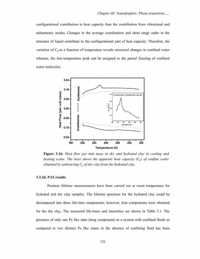
Figure 3.16 shows the conventional DSC curves for hydrated and dry clay in the
temperature range 200-298 K in the cooling and heating scans. In the hydrated clay, a
peak at T~ 230 K is observed during the cooling scan which becomes broader and shifts
to higher temperature during the heating scan. No transition peak is observed in dry clay
throughout the temperature range. Therefore, the peak observed in hydrated clay at T~
230 K is attributed to the freezing/melting or a similar phase transition of the confined
water. The broad nature of the peak does not allow us to determine the onset of transition
temperature and indicates that the phase transition spreads over a wide temperature range.
The presence of low temperature peak has been observed for water confined in variety of
porous media [Kozlowsk et al., 2012; Schreiber et al., 2001; Tombari et al., 2005] and
attributed to the depression in the freezing/melting behavior of water. The apparent
specific heat capacity Cp for water confined in clays calculated by Kozlowski et al. using
modulated DSC indicated the presence of partial freezing/inhomogeneous phases
[Kozlowsk et al., 2012]. However, different thermal characteristics have been observed in
different materials. In the present study, the observed low temperature peak may be
attributed to a low-temperature phase transition involving partial freezing of the confined
water.
The Cp of confined water is calculated by subtracting Cp of dry clay from the Cp of
hydrated clay as measured in temperature modulated mode and is shown in the inset of
Figure 3.16. The Cp of confined water is seen to be lower than the bulk water (4.18 Jg-1K-
1). This could be a manifestation of the effect of confinement as also suggested by
Kozlowski [Kozlowsk et al., 2012]. It is also observed that the obtained Cp increases with
the decrease in temperature and shows a maximum at ~230 K corresponding to the low-
temperature phase transition of confined water. The increase in Cp is an indicative of more
Chapter III: Nanodroplets: Phase transitions…..
121
configurational contribution to heat capacity than the contribution from vibrational and
anharmonic modes. Changes in the average coordination and short range order in the
structure of liquid contribute to the configurational part of heat capacity. Therefore, the
variation of Cp as a function of temperature reveals structural changes in confined water
whereas, the low-temperature peak can be assigned to the partial freezing of confined
water molecules.
3.3.2d. PAS results
Positron lifetime measurements have been carried out at room temperature for
hydrated and dry clay samples. The lifetime spectrum for the hydrated clay could be
decomposed into three life-time components; however, four components were obtained
for the dry clay. The measured life-times and intensities are shown in Table 3.1. The
presence of only one Ps like state (long component) in a system with confined fluids as
compared to two distinct Ps like states in the absence of confining fluid has been
Figure 3.16: Heat flow per unit mass in dry and hydrated clay in cooling and heating scans. The inset shows the apparent heat capacity (Cp) of confine water obtained by subtracting Cp of dry clay from the hydrated clay.
Chapter III: Nanodroplets: Phase transitions…..
122
observed by others too [Kajcsos et al., 2000; Dutta et al. 2006]. In the context of present
work, the observed result reveal localization of positron/Ps in nanoconfined water in clay.
Sample τ1
[ns] I1
[%] τ2
[ns] I2
[%] τ3
[ns] I3
[%] τ4
[ns] I4
[%]
Hydrated clay
0.226
(± 0.009)
38.42
0.490
(± 0.017)
43.63
2.115
(± 0.024)
17.94
-----
-----
Dry Clay
0.200 (±0.016 )
28.06
0.439
(± 0.015)
54.5
1.86
(± 0.066)
10.12
10.75
(± 0.200)
7.3
Figures 3.17 and 3.18 show the variation of S-parameter as a function of
temperature for dry and hydrated clay, respectively. The S-parameter profile for dry clay
(Figure 3.17) shows insignificant variation unlike the hydrated clay (Figure 3.18) which
shows distinct features over the studied temperature range in cooling as well as heating
cycle. The change of slope/discontinuity in S-parameter profile as a function of
temperature is indicative of phase transition of liquid confined in nanodomains [Dutta et
al., 2006 & 2008]. In the present context, the absence of variations in S-parameter profile
in the dry clay shows that the features seen in the hydrated clay are signatures of phase
transition of water confined in clay nanopores. Two phase transitions have been observed
for the confined water viz. above (high-temperature transition, HTT) and below (low-
temperature transition, LTT) the bulk freezing temperature (Figure 3.18) of water (273
K). The HTT and LTT range from 286-274 K and 254-240 K, respectively. Figure 3.18
also shows S-parameter profile for the heating cycle showing the presence of both the
transitions in addition to a marked hysteresis for HTT. The hysteresis behavior of
confined liquids has been observed by others and is explained on the basis of
thermodynamical stability of the phases taking into account surface energy barriers
Table 3.1: Positron lifetime and intensities at room temperature for the hydrated and dry clay sample
Chapter III: Nanodroplets: Phase transitions…..
123
Figure 3.18: Variation of S-parameter with temperature for hydrated clay in cooling (○) and heating (●) cycle.
[Morishige et al., 1999]. The origin of hysteresis observed in the present study could be
the inhomogeneities brought out by the strong surface interactions as well as the effect of
confining geometry [Brun et al., 1977; Vanfleet et al., 1995; Gross et al., 1997].
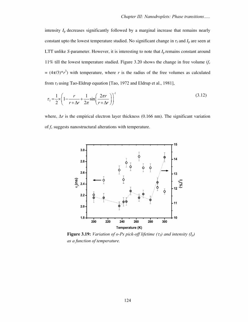
The variation of o-Ps pick-off life-time (τ3) and intensity (Ip) as a function of
temperature for hydrated clay are shown in Figure 3.19. It is seen that τ3 increases to a
maximum value (around T~268 K) after the completion of HTT, and, the corresponding
Figure 3.17: Variation of S-parameter with temperature for dry clay.
Chapter III: Nanodroplets: Phase transitions…..
124
intensity Ip decreases significantly followed by a marginal increase that remains nearly
constant upto the lowest temperature studied. No significant change in τ3 and Ip are seen at
LTT unlike S-parameter. However, it is interesting to note that Ip remains constant around
11% till the lowest temperature studied. Figure 3.20 shows the change in free volume (fv
= (4π/3)*r3) with temperature, where r is the radius of the free volumes as calculated
from τ3 using Tao-Eldrup equation [Tao, 1972 and Eldrup et al., 1981],
(3.12)
where, Δr is the empirical electron layer thickness (0.166 nm). The significant variation
of fv suggests nanostructural alterations with temperature.
1
31 1 21 sin2 2
r rr r r r
πτπ
−⎛ ⎞⎛ ⎞= × − + ⎜ ⎟⎜ ⎟+Δ +Δ⎝ ⎠⎝ ⎠
Figure 3.19: Variation of o-Ps pick-off lifetime (τ3) and intensity (Ip) as a function of temperature.
Chapter III: Nanodroplets: Phase transitions…..
125
The presence of two phase transitions, above and below the bulk freezing point of
water, is the first report on the phase behavior of nanoconfined water. Phase transition
below the bulk freezing temperature of water has been observed by many authors for
water confined in different geometries and assigned to supercooled water [Bruni et al.,
2011; Mallamace et al., 2006]. However, the transition seen at elevated temperature
(HTT) in the present study is observed for the first time for water confined in clay
nanopores. The shift in freezing/melting behavior has been explained on the basis of
nature of fluid-wall interaction [Miyahara et al., 1997; Radhakrishnan et al., 2002]. It has
been shown that the attractive interaction with the wall surface results in the elevation of
the freezing point, whereas, depression is observed in the case of repulsive (less
attractive) interaction. On this basis, we feel that the observed HTT (above bulk freezing
point), represents phase transition associated with the water molecules hydrogen-bonded
to cations as well as platelets surface (bound water). However, the concurrent presence of
a transition below the bulk freezing point (LTT) of water evidently reveals existence of
different regimes of confined water. In order to get further insight into these transitions
both NMR and DRS studies have been carried out as detailed in the latter section.
Figure 3.20: Variation of free volume (fv) with temperature. Error bar lies within the symbols.
Chapter III: Nanodroplets: Phase transitions…..
126
It is seen that the positron annihilation parameters viz. S-parameter, τ3 and Ip are
sensitive to phase transitions in confined systems and explore nanostructural alterations
following the transitions. The studies on phase transition of confined liquids have always
shown anomalous changes in S-parameter, τ3 and Ip near the transition. The onset of
transition is marked by a decrease in S-parameter similar to the present observation. The
completion is associated with the minimum in S-parameter which increases on further
cooling to a value similar to that at the onset of transition. This is explained on the basis
of structural inhomogeneities existing in the confined systems which include the presence
of inhomogeneous phases due to partial freezing, agglomeration or clustering of
molecules and the appearance of more surfaces and interfaces due to freezing [Dutta et
al., 2006 & 2008]. In addition, positron/Ps dynamics in the confined system viz.
trapping/detrapping and annihilation from delocalized states are also invoked to explain
the S-parameter and τ3 behavior.
While the two observed transitions are associated with significant change in
electron momentum distribution as reflected in S-parameter, it is interesting to note the
variation in free volume, fv. It significantly increases below HTT, reaches a maximum
(~268 K) and decreases till the lowest temperature studied. The variation of S-parameter
and fv at HTT suggest rearrangement of water molecules leading to structural ordering of
molecules near the surface. This ordering results into a new phase (configuration) with
large open/free volumes. On the other hand, at LTT, the variation in fv is not as
pronounced as S-parameter. Electron momentum distribution seems to be a more sensitive
index as compared to electron density associated with this transition. Although the exact
reason for this behavior is not known, a possible reason could be the fact that S-parameter
provides a composite information on p-Ps, free positron and o-Ps states unlike o-Ps life-
time (free-volume size). An empirical viscosity-free volume correlation i.e. η = A exp
Chapter III: Nanodroplets: Phase transitions…..
127
(1/fv) suggested by Miller indicates an inverse relation between fv and η [Miller et al.,
1963]. Therefore, the observed variation in fv (monotonic decrease) indicates increase in
the viscosity of water as temperature is lowered. This behavior corresponds to
supercooled liquids which become increasingly viscous as temperature approaches glass
transition, Tg (Tg of water is lower than the lowest temperature studied in the present
case). It is also to be noted that IP reduces to 11% below HTT and remains nearly same
till the lowest temperature studied (even below LTT). This indicates that confined water
does not completely freeze to crystalline ice at LTT. On the basis of these observations,
we conjecture that the LTT is associated with the supercooled water molecules.
3.3.2e. NMR results
NMR measurements have been performed in static and MAS mode for hydrated
clay sample. A single broad peak observed in static case is resolved into two distinct
peaks in MAS case coming from the confined water molecules (around 4 ppm) and Si–
OH groups (around 0 ppm) as shown in Figure 3.21. The confined nature of water trapped
inside the clay nanopores is the reason behind the extremely broad NMR peak of water
observed in static case. Anisotropic interactions like chemical-shift anisotropy and
dipolar-dipolar interactions are strong under these conditions. Partial averaging of these
interactions by MAS leads to narrower NMR peak of water.
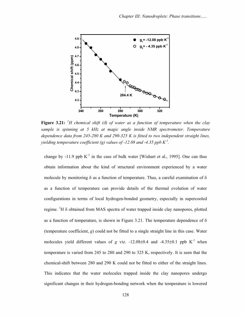
Isotropic chemical-shifts, δ, of nuclei like protons reflect the kind of electronic
environment experienced by them in a system. Any changes in the local electronic
environment of these nuclei will be accompanied by chemical-shift changes. Water
molecules form an extensive hydrogen-bonding network with each other. It has been
generally observed that the strength of this network weakens (lengthening of hydrogen-
bonds) with increase in temperature [Yamaguchi et al., 2001]. This change has a direct
influence on the 1H chemical-shifts of the water molecules, which for example, can
Chapter III: Nanodroplets: Phase transitions…..
128
Figure 3.21: 1H chemical shift (δ) of water as a function of temperature when the clay sample is spinning at 5 kHz at magic angle inside NMR spectrometer. Temperature dependence data from 245-280 K and 290-325 K is fitted to two independent straight lines, yielding temperature coefficient (g) values of -12.08 and -4.35 ppb K-1.
change by -11.9 ppb K-1 in the case of bulk water [Wishart et al., 1995]. One can thus
obtain information about the kind of structural environment experienced by a water
molecule by monitoring δ as a function of temperature. Thus, a careful examination of δ
as a function of temperature can provide details of the thermal evolution of water
configurations in terms of local hydrogen-bonded geometry, especially in supercooled
regime. 1H δ obtained from MAS spectra of water trapped inside clay nanopores, plotted
as a function of temperature, is shown in Figure 3.21. The temperature dependence of δ
(temperature coefficient, g) could not be fitted to a single straight line in this case. Water
molecules yield different values of g viz. -12.08±0.4 and -4.35±0.1 ppb K-1 when
temperature is varied from 245 to 280 and 290 to 325 K, respectively. It is seen that the
chemical-shift between 280 and 290 K could not be fitted to either of the straight lines.
This indicates that the water molecules trapped inside the clay nanopores undergo
significant changes in their hydrogen-bonding network when the temperature is lowered
Chapter III: Nanodroplets: Phase transitions…..
129
from 290 to 280 K. Moreover, g values in these two regimes reveal that the trapped water
resembles bulk-like water (in terms of hydrogen-bonding network) at lower temperatures
(T < 280 K), while it exists as a less mobile liquid at higher temperatures (T > 290 K) as
indicated by high g value of -4.35 ppb K-1. This region corresponds to the HTT, observed
in positron annihilation studies.
Figure 3.22: Transverse relaxation times (T2
* and T2′) of water as a function of temperature when clay sample is (a) static and (b) spinning at 5 kHz at magic angle inside NMR spectrometer. Dotted lines in both the plots indicate inflection points in the measured T2′ values as a function of temperature.
Chapter III: Nanodroplets: Phase transitions…..
130
Figure 3.22 shows the variation of T2* and T2′ values with temperature in static
(Figure 11a) and MAS (Figure 11b) modes. All the curves show two inflection points,
near 290 and 260 K. These inflection points are seen to be more pronounced in the case of
T2′ values obtained from the static mode. The variation of T2* and T2′ at 290 and 260 K
are indicative of change in dynamical properties of water and can be associated with the
phase transition of confined water. The transition at 290 K can be associated with the
change in local hydrogen-bonding network of water molecules as indicated by the change
in the value of temperature coefficient of 1H chemical-shift which leads to a structural
rearrangement of water molecules resulting in a network having bulk-like configuration.
We now correlate the changes observed in the structural and dynamical properties
of water confined in the clay nanopores as indicated by temperature coefficients (g) and
transverse relaxation times (T2* and T2′), respectively. At higher temperatures (T > 290
K), water exists as a less mobile liquid, with each molecule experiencing a strong
hydrogen-bonding network (g = -4.35 ppb K-1). The lowering of temperature in this
region decreases the mobility of water molecules and, as a result, transverse relaxation
times are shortened. The slow rise of transverse relaxation times when the temperature is
lowered from 290 to 260 K can be explained on the basis of partial
freezing/immobilization of water molecules resulting into two different regimes of
molecules whose relaxation times differ significantly.
The water molecules close to the platelet surface (hydrogen-bonded to the surface
as well as cations) get immobilized due to relatively attractive interaction with the surface
as compared to the molecules away from the surface. The relaxation time of these
immobile molecules falls off rapidly as compared to other molecules. The water
molecules which are away from the surface (relatively less bound) have mobility akin to
molecules present in bulk water as indicated by g value (-12.1 ppb K-1) and hence, yield
Chapter III: Nanodroplets: Phase transitions…..
131
much longer relaxation times. This scenario can be well understood from Figure 3.23,
wherein, eye guide (solid and dashed) indicate two regimes I and II of water molecules
representing faster relaxation of water molecules near the platelet surface and slower
relaxation due to the molecules away from the platelet surface, respectively. The resultant
of two relaxation processes results in the slow rise of T2′(T2*) from 290 to 260 K. As the
temperature is lowered further, the overall relaxation time is dominated more and more by
the water molecules in the regime II (bulk-like phase). Below 260 K, decrease in
transverse relaxation time indicates decrease in the mobility of water due to the decrease
in temperature.
3.3.2f. DRS results
Figure 3.24a and 3.24b show the three-dimensional plots of frequency (f) and
temperature dependence of the measured dielectric loss i.e. imaginary part of permittivity
(ε″(f)) in hydrated and dry clay, respectively. The dielectric response of the two samples
are significantly different throughout the studied temperature range.
Figure 3.23: Transverse relaxation time (T2′) of water as a function of temperature obtained in the static mode. Solid and dashed lines (eye guides) represent the likely scenario of the freezing phenomenon of water layers.
Chapter III: Nanodroplets: Phase transitions…..
132
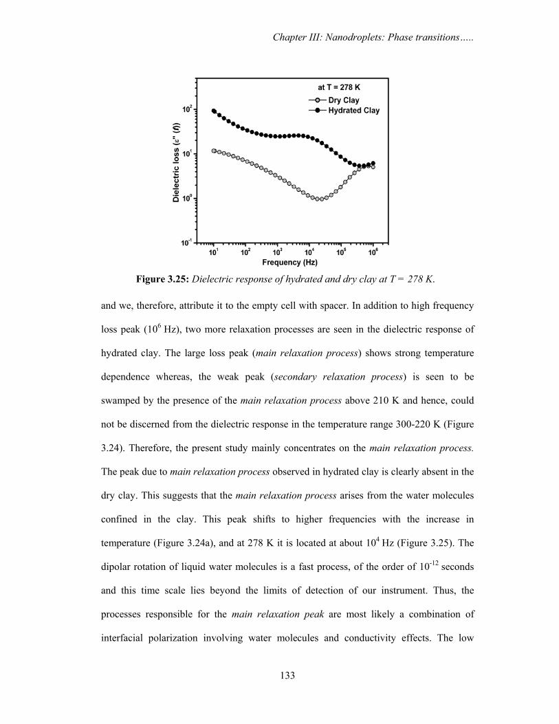
Figure 3.25 shows the dielectric response at T = 278 K for both the samples,
which indicates different relaxation processes in the two cases. The strong loss peak near
106 Hz is present in both the samples and does not show any temperature dependence.
This peak is also present in the dielectric response of empty cell with the Teflon spacer,
Figure 3.24: Three dimensional representation of temperature and frequency dependence of imaginary part of the dielectric permittivity (ε′′(f)) or dielectric loss for (a) hydrated and (b) dry clay.
Chapter III: Nanodroplets: Phase transitions…..
133
and we, therefore, attribute it to the empty cell with spacer. In addition to high frequency
loss peak (106 Hz), two more relaxation processes are seen in the dielectric response of
hydrated clay. The large loss peak (main relaxation process) shows strong temperature
dependence whereas, the weak peak (secondary relaxation process) is seen to be
swamped by the presence of the main relaxation process above 210 K and hence, could
not be discerned from the dielectric response in the temperature range 300-220 K (Figure
3.24). Therefore, the present study mainly concentrates on the main relaxation process.
The peak due to main relaxation process observed in hydrated clay is clearly absent in the
dry clay. This suggests that the main relaxation process arises from the water molecules
confined in the clay. This peak shifts to higher frequencies with the increase in
temperature (Figure 3.24a), and at 278 K it is located at about 104 Hz (Figure 3.25). The
dipolar rotation of liquid water molecules is a fast process, of the order of 10-12 seconds
and this time scale lies beyond the limits of detection of our instrument. Thus, the
processes responsible for the main relaxation peak are most likely a combination of
interfacial polarization involving water molecules and conductivity effects. The low
Figure 3.25: Dielectric response of hydrated and dry clay at T = 278 K.
Chapter III: Nanodroplets: Phase transitions…..
134
Figure 3.26: Dielectric response ((ε′′(f)) vs. f) for hydrated clay at 250 K. The solid line represents the fit to the response using sum of power law and HN function; dotted and dash-dot curves represent the main relaxation process and d.c. conductivity contribution, respectively.
frequency dispersion is observed in both the samples and is ascribed to conductivity
contribution from the sample. It may also be noted that the weak loss feature at lower
temperatures in dry clay is qualitatively different from that observed in hydrated clay, and
must therefore, have a different origin. Further analysis of the main relaxation process to
obtain relaxation times has been carried out by fitting the dielectric response curves (ε″(f)
vs. f ) with the sum of a power law (d.c. conductivity) and a well known Havriliak-
Negami (HN) function,
( )( )[ ] ⎥
⎥⎦
⎤
⎢⎢⎣
⎡
+
Δ+= −
βαωτ
εωεσ
ωεi
n
o
DC
1Im"
(3.13)
where, ω = 2πf, Δε = εS-ε∞, where, εS and ε∞ are static and high frequency limiting values
of the dielectric constant, respectively, εo is the permittivity of free space, σDC is the
conductivity contribution, τ is the relaxation time and n, α and β are empirical exponents
with values between 0 and 1. As an example of this fitting, the dielectric loss spectrum of
the hydrated clay at 250 K is shown in Figure 3.26.
Chapter III: Nanodroplets: Phase transitions…..
135
The main relaxation process is the only dominant relaxation observable at this
temperature and is shown with a dotted curve along with the conductivity contribution.
For the spectra at temperatures below 210 K, two HN functions are required to fit the
dielectric response. However, due to small amplitude of second relaxation process at low
temperatures (below T=210 K) it could not be discerned from the response curve.
In the case of dry clay, the only relaxation process apart from the low frequency
dispersion shows weak loss in the temperature range 298-210 K. This process is seen to
be different from that observed in hydrated clay, and shows Arrhenius temperature
dependence of relaxation time over the studied temperature range. The activation energy
of this process is found to be EA ≈ 0.72 eV, which is higher than that for the process
observed in hydrated clay (Table 3.2, discussed below). The origin of this process is not
clear but this feature is not observed in hydrated clay where it might have been swamped
by low frequency dispersion.
The relaxation time τ corresponding to the main relaxation process in hydrated
clay shows strong temperature dependence over the range 298-210 K. The plot of
temperature dependence of τ is given in Figure 3.27. It is interesting to note that the
relaxation time, τ follows Arrhenius behavior at temperatures below 240 K and a non-
Arrhenius behavior above 240 K. In fact, above 240 K, the behavior could be very well
approximated by a Vogel-Fulcher law (see below). The temperature dependence of τ for
the main relaxation process are fitted as,
( ) ⎟⎟⎠
⎞⎜⎜⎝
⎛=
TkE
TB
ao expττ
for T ≤ 240 K (3.14)
( ) ( )⎟⎟⎠
⎞⎜⎜⎝
⎛−
=o
oo TT
BTT expττ
for T ≥ 240 K (3.15)
Chapter III: Nanodroplets: Phase transitions…..
136
Figure 3.27: Temperature dependence of relaxation time (τ) for the main relaxation process in hydrated clay, fitted to Arrhenius (210-235 K) and Vogel-Fulcher (240-300 K) functions.
where, Ea is activation energy, kB is Boltzmann constant, T is the temperature, B is a
dimensional normalization factor, τ0 is a pre-exponential factor and To is Vogel-Fulcher
(VF) temperature. The best fit values for the Arrhenius and VF behavior are tabulated in
Table 3.2.
Arrhenius Fit Vogel-Fulcher Fit
Parameter Value Parameter Value
Ea 0.257 eV E 0.027 eV
τ0 7.17x10⁻⁹ s τVF 5.34x10⁻⁷ s
----- ---- TVF 200 K
The variation of relaxation time with temperature shows that the dynamics of
water confined in clay nanopores shows a cross over from non-Arrhenius to Arrhenius
Table 3.2: Fitting parameters for hydrated clay; Arrhenius fit (T< 240 K) and Vogel-Fulcher fit (T> 240 K).
Chapter III: Nanodroplets: Phase transitions…..
137
temperature dependence around 240 K. However, the values of the relaxation times are
much slower than those reported for rotational dynamics of water molecules [Swenson et
al., 2000; Bergman et al., 2000] and hence cannot be attributed to these processes. As
mentioned earlier, this relaxation may be a combination of interfacial polarization and
conductivity effects involving the water molecules. Even so, the cross over from one type
of temperature dependence to another, as observed in Figure 3.27, suggests a transition.
This change in behavior near 240 K matches well with the low-temperature transition
observed in our positron annihilation study. Since conductivity effects are likely to be
dominant in liquid water as compared to frozen water, we may infer that substantial
amount of liquid water exists above 240 K. On this basis, we may conjecture that the
observed cross over at 240 K is related to the partial freezing of supercooled water which
results in the change in conductivity contribution owing to the frozen phase of water.
3.3.2g. Discussion
Two phase transitions viz. above (HTT) and below (LTT) the bulk freezing
temperature of water have been observed for water confined in clay nanopores. PAS is
seen to be sensitive to both the transitions unlike other techniques. While DSC and DRS
are not sensitive to HTT, NMR provides the strongest evidence of structural and
dynamical changes associated with this transition. As discussed earlier, two layers of
water molecules can be accommodated between the clay platelets. These water molecules
exist in two different regimes, molecules hydrogen-bonded to platelet surface as well as
cations are more bound as compared to the molecules away from the surface [Skipper et
al., 1991]. Based on our earlier studies, HTT is expected to be associated with the
molecules experiencing more attractive interactions with the surface of the platelets.
NMR study reveals that HTT is associated with the structural rearrangement of water
molecules as reflected in the variation of 1H chemical-shift with temperature. The change
Chapter III: Nanodroplets: Phase transitions…..
138
of slope of chemical-shift with temperature (g) from -4.35 to -12.08 ppb/K around 284.4
K indicates alteration in hydrogen-bonded network of water molecules. The increase in τ3
and S-parameter below HTT signify structural alterations in terms of increase in free
volume/open space and is consistent with NMR observation. The transverse relaxation
time measured in NMR reveals change in dynamical properties of water molecules at
HTT. The slow rise around 290 K (near HTT) is explained on the basis of different
relaxation times which have arisen due to the existence of different regimes of confined
water (discussed earlier). This has been correlated to the immobilization of water
molecules (faster relaxation) close to the platelet surface (bound molecules) as compared
to the slower relaxation of molecules away from the platelet surface. It is also to be noted
that a marked hysteresis is observed for HTT in PAS owing to thermal stability of the
phases at the surface. On the basis of NMR and PAS results, HTT is expected to be
associated with the phase behavior of water molecules bound to the platelet surface i.e.
immobilization of these water molecules together with the structural rearrangement of
confined water. Below HTT, rest of the water molecules tend to form hydrogen-bonded
network and behave as bulk-like phase as reflected from the variation of 1H chemical-
shift with the decreasing temperature (g = -12.08 ppb/K).
The presence of LTT is observed from PAS, DSC and DRS. This transition can be
related to water molecules forming hydrogen-bonded network similar to bulk water (g = -
12.08 ppb/K). The S-parameter has shown significant change at this transition unlike fv, IP
and 1H chemical-shift. The change in S-parameter can be explained on the basis of
alteration in electron momentum distribution owing to the change in the phase behavior
of water at this temperature. The significant and nearly constant value of IP (~11%) shows
that the confined water does not freeze till the lowest temperature studied. In DSC, a peak
has been observed corresponding to LTT. This low temperature peak has been attributed
Chapter III: Nanodroplets: Phase transitions…..
139
to the depression in freezing/melting point of confined water by many authors. However,
its correspondence to incomplete freezing has been explained by Kozlowski et al. Though
DRS is sensitive to relaxation dynamics of molecules (dipolar relaxation), in the present
case, the measured relaxation time corresponds to the combination of interfacial
polarization and conductivity contribution from the sample. This relaxation process
shows a cross over from non-Arrhenius to Arrhenius behavior around 240 K. The
observed cross over in the behavior of relaxation time can be correlated to change in the
phase behavior which results in the change in conductivity contribution of the sample.
Though no clear evidence for any structural or dynamical change for confined water is
observed at LTT, the results from PAS, DSC and DRS indicate incomplete freezing
and/or depression in freezing /melting point of confined water.
3.4. Conclusions
Phase transitions in nanodroplets (ethylene glycol and isopropanol confined in
ZSM 5 and, water confined in saponite clay) have been studied using different techniques
viz. PAS, NMR and DRS. The structural and dynamical properties were indexed to probe
the phase transitions. The effect of fluid-surface interfacial interaction on the
freezing/melting point of confined ethylene glycol and isopropanol was examined. An
elevation in the freezing/melting point was seen and attributed to the attractive interaction
between the liquids and wall of the confining geometry (ZSM 5). However, the strength
of the (attractive) interaction has significant influence on the extent of the shift, as clearly
seen from different degree of shifts in the two cases. The strong interaction in the case of
isopropanol owing to inter-molecular hydrogen bonding resulted in higher degree of shift
in contrast to ethylene glycol where, due to both inter- and intra molecular hydrogen
bonding the effective interaction with the surface is weaker.
Chapter III: Nanodroplets: Phase transitions…..
140
The phase behavior of nanoconfined water in slit like pores of saponite was
studied. The effect of strong hydrogen bonding between water molecules as well as water
molecules and the surface of platelet strongly influence the structural and dynamical
properties of confined water. Two phase transitions viz. above (HTT) and below (LTT)
the bulk freezing temperature of water were observed and attributed to different regimes
of confined water (role of interfacial interactions). The presence of HTT is the first report
on the phase behavior of nanoconfined water. The structural and dynamical parameters
suggest that HTT involves structural modification in terms of hydrogen-bonded network
and dynamic arrest/immobilization of water molecules close to the platelet surface owing
to attractive interaction with the surface. On the other hand, LTT is conjectured to be
associated with the partial freezing of confined water as evident from PAS, DRS and
DSC. The present study mainly highlights the effect of role of interfacial interaction on
the phase transition of confined liquids.
Chapter IV: Pore architecture of…..
141
CHAPTER-IV
Pore architecture of membranes
Chapter IV: Pore architecture of…..
142
Membranes based processes are an active area of interest for scientific community
engaged in developing new membranes and understanding the microscopic aspects of
their transport mechanism. Membrane processes are broadly divided on the basis of the
intrinsic pore sizes in liquid as well as gas permeation based separation schemes. For
example, reverse osmosis, pervaporation as well as gas separation schemes have pore
sizes below 0.8 nm while nanofiltration of liquid or gas separation using ceramic
membranes have pore sizes in the range of 0.8 to 1.5 nm. Ultrafiltration for liquid
permeation refers to pore sizes 2-60 nm, whereas membranes with pore sizes larger than
60 nm are used in microfiltration processes. In the dense and homogeneous polymer
membranes with pore sizes smaller than 1 nm, the mechanism is primarily known as
solution-diffusion model where the permeability is given as the product of diffusion
coefficient and solubility of liquid or gas, as the case may be, in the polymer matrix
[Baker et al., 2004].
Hydrophobic supported liquid membranes (SLMs) having pore sizes larger than
100 nm provide a nice alternative to conventional liquid-liquid extraction process such as
solvent extraction [Luque et al., 2000; Allen et al., 1999 and Baker et al., 1977]. In recent
years, SLMs have received considerable attention for the recovery of metallic ions from
waste water streams due to its characteristics such as low energy consumption, high
selectivity and rapid extraction capacity factor. SLM extraction is based on three phase
system with an organic phase sandwiched between two aqueous phases (inset Figure 4.1)
[Joensson et al., 1992, Barcelo et al., 1997 and van de Merbel et al., 1993]. The organic
phase containing the metal ion selective extractant and solvent is immobilized in a porous
hydrophobic membrane. This membrane acts as an intermediary separating the feed
phase, which contains the species to be removed, and the stripping phase in which the
species to be transferred is recovered [Reyes-Aguilera et al., 2008]. As in solvent
Chapter IV: Pore architecture of…..
143
extraction, the extractant is responsible for the extraction of the species of interest; in this
case, however, the extraction and recovery processes are carried out simultaneously, with
the advantage that, unlike solvent extraction, SLM uses minimum quantities of organic
phase [Valenzuela et al., 1993], which allows the use of highly selective extractants and
diminishes the risk of environmental contamination at the same time. The transport
mechanism that dictates this process has two steps (i) the exchange of metal ion in the
feed side which is a fast process and (ii) the diffusion of metal-extractant complex which
is a slow process, primarily Fickian in nature. Overall, the mechanism is solution-
diffusion in nature as described earlier for the dense homogeneous phase, only difference
being that the solubility term is equivalent to the fast exchange process at the surface. The
diffusion of the metal-extractant complex (Fickian) across the membrane thickness is
similar to that used in the dense homogeneous phase (Figure 4.1).
Membrane permeability and transport properties are governed by the structural
characteristics like pore architecture of the membrane which essentially refers to pore
Figure 4.1: SLM based three phase extraction system.
Chapter IV: Pore architecture of…..
144
size, its distribution, pore fraction, porosity and pore interconnectivity. There are a host of
techniques such as small angle X-ray/neutron scattering (SAXS/SANS), gas absorption
techniques, ellipsometric porosimetry, electron microscopy that can characterize the size
as well as pore fraction, however, they fail to evaluate the extent of pore
interconnectivity. In this regard, positron annihilation spectroscopy (PAS) can be used as
a probe to characterize pore architecture not only in terms of pore size, pore size
distribution, pore fraction, porosity (open/closed) but also to evaluate the pore
interconnectivity through the evaluation of positron/Ps mobility in porous materials.
Essentially, the mean free path of Ps in the pores gives an idea about the length scale over
which pores may be interconnected thus providing a complete idea about the pore
architecture. Figure 4.2 represents the positron/Ps behavior in a porous membrane
containing closed, open and interconnected pores. Positron injected into the porous
system forms Ps and then diffuses within the porous network by making collisions with
the walls of the pores. In the event of highly porous network or in vacuum, annihilation
from the intrinsic triplet state (3γ annihilation) is enhanced. Ps escaping into the vacuum
(3γ annihilation) is a telltale indicator of highly porous (open porosity) and interconnected
network. The technique involves slow positron beam depth profiling to obtain
annihilation profile in the porous membrane, which is used to evaluate Ps
diffusion/mobility within the porous network. The 3γ/2γ ratio is mainly used to
characterise porosity or Ps reemission from surfaces [Petkov et al., 2001 and 2003;
Gidley et al., 2006] through the evaluation of Ps diffusion length inside the membrane
using VEPFIT analysis.
In the present work, polytetraflouroethylene (PTFE) SLMs and track etched
polycarbonate (PC) membranes have been studied for their pore architecture using slow
positron beam depth profiling. The 3γ/2γ profile has been utilized as a measure of
Chapter IV: Pore architecture of…..
145
porosity and interconnectivity of pores through Ps diffusion length in the membranes
obtained by fitting the profiles. A correlation between the pore architecture and
permeability of metal ions through the membranes (PTFE) has been observed.
4.1. Materials
Two varieties of commercially available macroporous membranes viz. PTFE
SLMs (70 μm) and track etched PC membranes (25 μm) with quoted pore size in the
range of 0.2-5 μm and 0.03-0.2 μm, respectively have been studied for their pore
architecture. The membrane surface has been coated with 10 nm gold diffusion layer
deposited by vacuum evaporation. The track etched PC membranes were obtained from
Whatman Asia Pacific Private Ltd. These membranes were formed by the bombardment
of medium mass charged particles with sufficient energy to perforate 10 µm
polycarbonate sheets in the charged particle accelerator. After irradiation with charged
particles, these membranes were subjected to chemical etching to form cylindrical pores
having desirable diameter. The pores formed in these membranes have straight cylindrical
shape.
Figure 4.2: Schematic of positron/Ps behavior in a porous membrane containing closed, open and interconnected pores [Gidley et al., 2006].
Chapter IV: Pore architecture of…..
146
4.2. Experimental Techniques
4.2.1. Conventional characterization of the membranes
Figure 4.3: SEM images of PTFE SLMs with pore sizes as; A (0.2 μm), B (0.45 μm), C (1.2 μm) and D (5.0 μm). Yellow line indicates 50 μm length scale.
A B
C D
Chapter IV: Pore architecture of…..
150
4.3.1a. Surface morphology and chemical nature
Surface morphology of the membranes as characterized by SEM is shown in
Figure 4.3. SEM images show that these membranes have different surface morphology
and can be categorized into two classes. Membranes A and B show granular structure
with small pores, whereas membranes C and D show fibre like structure with large open
pores. The porosity data (Table 4.1) for the membranes is seen to be consistent with the
morphology. Figure 4.4 shows the ATR-FTIR spectra for all the membranes. The
presence of only two peaks at 1275 cm-1 and 1205 cm-1 characteristics of PTFE
corresponding to C-C and C-F bonds ensures that there are no other chemical impurities
that might influence the Ps formation probabilities.
4.3.1b. Small angle X-ray scattering
Experimental corrected SAXS profiles are shown in Figure 4.5. The profiles for
all the membranes are seen to be similar and vary as q-4 in the high-q region suggesting
smooth surface for the scattering objects (pores in the present samples). The SAXS
Figure 4.4: ATR-FTIR spectra of PTFE SLMs.
0.0
0.4
0.8
2500 2000 1500 1000 500
0.0
0.4
0.8
0.0
0.4
0.8
0.0
0.4
0.8
Wavenumber (cm-1)
Membrane-A
Abs
orba
nce
Membrane-B
Membrane-D
Membrane-C
Chapter IV: Pore architecture of…..
151
intensity I (q) from an ensemble of pores or particles having uniform shape and poly-
dispersity in size can be expressed as [Gunier et al., 1955 and, Glatter et al., 1982],
dRRVRNRqPCqI ∫= 2))()((),()( (4.3)
where, C is independent of ‘q’ but depends on the scattering length density contrast
between the solid matrix and pore and, number density of the pores. P(q, R) is square of
the scattering form factor for particle of radius R. The expression for P(q, R) for spherical
scattering objects is [Gunier et al., 1955 and, Glatter et al., 1982],
2
3),()),cos(),(sin(3),( ⎥⎦
⎤⎢⎣
⎡ −=
RqRqqRRqRqP (4.4)
where, V(R) is volume of the pore of radius R and N(R) is the pore radii distribution
function. The limits of integration depend on the q-range of the profiles. For log-normal
distribution, N(R) is given by [Aitchison et al., 1957],
[ ]⎥⎦
⎤⎢⎣
⎡−=
2
222 2)/ln(exp
21)(
σπσoRR
RRN (4.5)
0.1 1100
102
104
106
Inte
nsity
(arb
.u.)
q (nm-1)
Membrane AMembrane BMembrane CMembrane D
Figure 4.5: Experimental corrected SAXS profiles.
Chapter IV: Pore architecture of…..
152
where, Ro and σ are parameters of the distribution. Figure 4.6 shows fit to the data for
membrane A (quoted pore size 200 μm) and the pore size distribution (inset). From the
fitted parameters, the mean radius (<R>) of the pores is estimated using the relation, <R>
= Ro exp (σ2/2) whereas, the variance in the distribution is given by, w = [<R2>-<R>2]1/2.
The size of the pores as estimated by SAXS is, <R> = 38.3 nm and w = 29.5 nm. It has
been observed that all the membranes contain pores of 38.3 nm size.
4.3.1c. Positron annihilation life time spectroscopy
PALS measurement has been deliberately carried out with small time dispersion
to evaluate the smaller pores (free-volume) as, 39 nm (measured from SAXS) and the
quoted larger pores would yield the near saturation life-time of o-Ps i.e. 142 ns. Pick-off
o-Ps life-time (τ3), intensity (I3) and average pore size estimated using TE equation (Eq.
1.5) are given in Table 4.2. It is seen that Ps intensities and life time are nearly equal in all
the membranes and all the membranes contain pores in the range of 0.26-0.29 nm.
0.1 1100
102
104
106
108
0 20 40 60 80 100 120 140 1600.000
0.005
0.010
0.015
0.020
0.025
Pore
size
dist
ribut
ion
Pore radius (nm)
Inte
nsity
(arb
.u.)
q (nm-1)
Exp. Data Fitted Data
Figure 4.6: Fit to the experimental SAXS profile for membrane A; inset shows the obtained pore size distribution.
Chapter IV: Pore architecture of…..
153
Table 4.2: o-Ps life life-time, Intensity and calculated pore size (PALS measurement)
Membranes o-Ps pick-off lifetime, τ3 (ns)
Intensity, I3 (%)
Radius
(nm)
A 1.92 5.99 0.28
B 1.76 6.22 0.26
C 1.98 7.03 0.29
D 1.82 5.59 0.27
4.3.1d. Doppler broadening and 3γ/2γ annihilation spectroscopy
The S-parameter and 3γ/2γ ratio as a function of positron energy (depth) for all the
membranes (as received/pristine) are shown in Figure 4.7 and 4.8, respectively. The S-
parameter profiles are seen to be flat and no significant difference has been observed for
membranes A, B, C and D. This is similar to the behavior of S-parameter in nonporous
PTFE. Flatness of the profiles in the present case may also be due to the highly porous
nature of the membranes. It is, therefore, not useful in elucidating any information on Ps
0 2 4 6 8 100.54
0.55
0.56
0.57
0.58
0.59
0.60Membrane AMembrane BMembrane CMembrane D
S- p
aram
eter
Positron energy (keV)
Figure 4.7: The S-parameter profile for pristine PTFE SLMs. Error on the data is indicated on one of the data points in the figure.
Chapter IV: Pore architecture of…..
154
mobility. The 3γ/2γ profile (Figure 4.8), on the otherhand, shows distinct changes with
positron incident energy as well as between the membranes. The profiles carry
information about the Ps mobility and fitted using VEPFIT to extract Ps diffusion length
(L+). The fit to the experimental data, represented by solid lines is shown in Figure 4.9.
The diffusion lengths are seen to be 39, 102, 72 and 107 nm for membrane A, B, C and D,
respectively. The obtained diffusion length in the case of membrane C and D are seen to
be very small inspite of the large size of pores as compared to membrane A and B. It is
seen from SEM that membrane C and D have different morphology compared to A and B.
Also, the porosities in the former are larger. From the measured Ps diffusion length it is
seen that although there is a sharp increase in L+ going from A to B, the values for C and
D seem to be underestimated considering the porosity and morphology.
In order to get a better understanding in to this aspect, 3γ/2γ profile for the
membranes B and C (one membrane from either category) with a surface diffusion layer
of gold (10 nm) has been measured. This prevents Ps from escaping in to the vacuum that
0 2 4 6 8 10
0.80
0.84
0.88
0.92
0.96
1.00
3γ
/2γ r
atio
Membrane AMembrane BMembrane CMembrane D
Positron energy (keV)
Figure 4.8: The 3γ/2γ profiles for pristine PTFE SLMs. Error on the data is same for all the membranes and is shown for one of the membranes in the figure.
Chapter IV: Pore architecture of…..
155
might modify 3γ/2γ profile. The 3γ/2γ profile for goldcoated and the pristine membranes
(B and C) are compared in Figure 4.10.
Figure 4.9: VEPFIT analysis of 3γ/2γ ratio for PTFE SLMs. Solid lines represent fit to the experimental data.
0 2 4 6 8 100.80
0.84
0.88
0.92
0.96
1.00
1.04
1.08
3γ/2γ r
atio
Positron energy (keV)
0.80
0.84
0.88
0.92
0.96
1.00
1.04
1.08
Membrane B
Membrane C
Figure 4.10: 3γ/2γ profiles for Pristine and goldcoated PTFE (soild symbols) membranes B and C.
Chapter IV: Pore architecture of…..
156
At thermal velocity, Ps can travel a substantial distance away from the surface
prior to annihilation. Considering the experimental arrangement (detector perpedicular to
sample), Ps escape from the membrane surface due to open surface porosity has resulted
in the decrease in 3γ detection leading to decrese in 3γ/2γ ratio in the surface region. In
the case of membrane C, the open porosity on the surface seems to be much higher than
the membrane B as reflected from the large difference in 3γ/2γ ratio (surface region) in
the former. The fitting of 3γ/2γ profiles obtained in the case of goldcoated membranes
show much higher L+ viz. 400 and 3000 nm for B and C, respectively as compared to 102
and 72 in the corresponding pristine membranes. By preventing Ps to escape from the
surface and make them coral within the membrane reveals the true picture of the pore
architecture of the membranes. The L+ is related to the mean free path of Ps and hence,
measure of pore interonnectivity. The obtained L+ indicate that pore interconnectivity is
much higher in the case of fibrous membranes (C and D) as compared to membrane A
and B having granular structure.
4.3.1.e. Permeability of metal ions and transport properties
Figure 4.11 shows the permeabilty of Pu+3 and Am+3 for all the four membranes
(A, B, C and D) with TODGA as extractant, n-dodecan as solvent and nitric acid in feed
as well as receiver cells. A systematic decrease in permeability is seen from A to D ( i.e.
increase in pore size) under identical condition. Similar trend has also been seen in earlier
studies on the permeation of UO22+ through identical PTFE SLMs [Mohapatra et al., 2006
and Lakshmi et al., 2004]. It is known that permeability is proportional to φR2 (R being
radius of pore) and inversely proportional to the thickness of the membrane [Baker,
2004]. The latter being identical in all the membranes, the permeability should have been
highest in the case of membrane D contrary to what is observed in the present study.
Chapter IV: Pore architecture of…..
157
0.001
0.002
0.003
B DCA
P (c
m/s
ec)
Membrane
L + (nm
)
40
80
120 (c)
(b)
(a)
0.000
0.002
0.004
Am(III)
Pu(III)
Figure 4.12: Correlation between Permeability of ions in PTFE membranes and Ps diffusion length.
0.0005
0.0010
0.0015
0.0020
0.0025
0.0030
0.0035
DCBA
Perm
eabi
lity
(cm
/s)
Membrane
Pu(lll) Am(lll)
Figure 4.11: Permeability of Pu (lll) and Am (lll) through PTFE membranes.
Chapter IV: Pore architecture of…..
158
An inverse correlation between the permeability and L+ has been observed for
PTFE SLMs (Figure 4.12) i.e. higher the L+, lower is the permeability. A systematic
increase in L+ can be ascribed to increase in pore interconnectivity or pore overlap,
resulting in enhancement in the mean free path of the Ps atom. Such interconnection of
pores provides alternative path to the diffusing metal ion complex which could be longer
than the thickness of the membrane it has to travel to reach the receiver compartment.
Overall this would result in increase in the time taken by the metal ions to permeate
through the membrane resulting in decrease in permeability. In the parlance of membrane
science this is referred to as tortuosity. Permeability scales inversely with tortuosity i.e.
higher the tortuosity lower is the permeability [Baker et al., 2004]. Pore interconnectivity
is the main microscopic reason for the increase in the tortuosity in a membrane as evident
from the measured L+. The large pore interconnectivity is seen to have deleterious effect
on the permeability (inverse relation between the two) of metal ions through the
membrane.
Colating all the information from conventional as well as positron beam studies,
an impression of pore architecture of the studied membranes (granular and fibrous) is
depicted in Figure 4.13. As seen, pore overlap increases in the case of fibrous membrane
Figure 4.13: Impression of pore architecture in porous membranes.
Chapter IV: Pore architecture of…..
159
having large size pores, resulting in large interconnectivity between the pores. Also,
fibrous membrane have high open porosity. The solid lines represent the path taken by the
metal ion complex across the membrane. Pore overlap (interconnection) is seen to
provide alternative tortuous path to metal ions resulting in lowering of permeability.
4.3.2. Track etched polycarbonate membranes
4.3.2a. Surface morphology
Figure 4.14a shows the SEM image of one of the track etched nuclepore PC
membranes showing the presence of cylindrical through and through pores. Distinct
morphology of track etched PC membrane as compared to fibrous membrane (PTFE
SLM) having highly interconnected pores is clearly evident from Figure 4.14b. In the
present study PC membranes with pore size 0.03, 0.2 and 0.4 μm are named as membrane
1, 2 and 3, respectively.
4.3.2b. Doppler broadening and 3γ/2γ annihilation spectroscopy
The variation of S-parameter as a function of positron energy for membranes 1-3
are shown in Figure 4.15. The S-parameter profile is almost featureless throughout the
energy range owing to the highly porous nature of the membranes. As the pore size is
large (order of μm) in these membranes, o-Ps pick-off annihilation is expected to be
Figure 4.14: SEM images of (a) track etched PC and, (b) fibrous PTFE SLM. Yellow lines indicates the length scale of measurement; (a) 6 μm; (b) 50 μm
Chapter IV: Pore architecture of…..
160
insensitive to the pore sizes and most of the o-Ps annihilate by 3γ annihilation. The
energy spectroscopy (3γ/2γ), which directly senses the formation and complete history of
long-lived 3γ decay of o-Ps, is seen to be a more sensitive technique for the investigation
of pore architecture in these membranes. In addition, similar to earlier observation in
PTFE SLMs, open porosity due to large pore size may modify the 3γ/2γ profiles and
hence, corresponding goldcoated membranes are also studied in order to get true picture
of pore architecture in these membranes. The 3γ/2γ profiles for PC membranes are shown
in Figure 4.16 indicating distinct variation between the membranes. The quantitative
analysis for the observed variations is carried out by evaluating L+ using VEPFIT. The L+
obtained by fitting the 3γ/2γ profiles are 55, 30 and 76 nm for membrane 1, 2 and 3,
respectively. No systematic trend in L+ is seen with the increase in the pore size. Based
on our earlier observations (PTFE SLMs), for large size pores (micron range) and highly
porous membranes, the escape of Ps from the surface modifies the profiles resulting in
underestimation of L+. In such cases, true pore architecture can be obtained by capping
the membrane surface with gold layer to prevent Ps escape from the surface. The S-
0 4 8 12 16 200.52
0.53
0.54
0.55
0.56
0.57
0.58
0.59
0.60 Membrane 1 Membrane 2 Membrane 3
S-pa
ram
eter
Positron energy (keV)
Figure 4.15: The S-parameter profile for pristine track etched PC membranes; Membrane 1 (0.03 μm), Membrane 2 (0.2 μm) and Membrane 3 (0.4 μm).
Chapter IV: Pore architecture of…..
161
Figure 4.16: 3γ/2γ profiles for pristine track etched PC membranes.
0 4 8 12 16 20
0.76
0.80
0.84
0.88
0.92
3γ/2γ r
atio
Positron energy (keV)
Membrane 1 Membrane 2 Membrane 3
parameter and 3γ/2γ profile for goldcoated PC membranes are shown in Figures 4.17 and
4.18, respectively. No significant variation is S-parameter with depth has been observed
owing to the porous nature of the membranes and hence, it cannot be used to elucidate
any information about the pore architecture. However, it indicates that Ps yield in all the
membranes is same. On the otherhand, 3γ/2γ profiles for goldcoated membranes show
distinct behavior as compared to their pristine forms. The measured L+ for goldcoated
membrane 1, 2 and 3 are 375, 255 and 330 nm, respectively.
0 2 4 6 8 10 12
0.58
0.59
0.60
0.61
0.62
0.63 Membrane 1 Membrane 2 Membrane 3
S-pa
ram
eter
Positron energy (keV)
Figure 4.17: The S-parameter profile for goldcoated PC membranes.
Chapter IV: Pore architecture of…..
162
As also observed in PTFE SLMs, the profile obtained in the case of goldcoated
membranes represent the true reflection of pore architecture of the membranes. It is seen
that the obtained L+ is much larger than the pore size in the case of membrane 1 in
contrast to membranes 2 and 3 where, L+ is of the order of the pore size. This indicates
that pores in the membrane 1 are highly interconnected as compared to membrane 2 and
3, where cylindrical through and through pores are present. The L+ is related to the cross
section of pores in the latter case. Also, a marginal difference in 3γ/2γ ratio at the surface
has been observed for pristine and goldcoated membranes depicting open porosity.
It is also to be noted that the obtained L+ in the case of track etched PC
membranes are much smaller than that in fibrous PTFE SLMs indicating distinct
microstructure of the membranes especially in terms of pore interconnection. The fibrous
membranes show higher degree of pore interconnectivity (large L+) than the track etched
PC membranes where cylindrical through and through pores are present.
Figure 4.18: 3γ/2γ profiles for goldcoated PC membranes.
0 2 4 6 8 10 12 14
0.70
0.72
0.74
0.76
0.78
0.80
0.82 Membrane 1 Membrane 2 Membrane 3
3γ/2γ r
atio
Positron energy (keV)
Chapter IV: Pore architecture of…..
163
4.4. Conclusions
The pore architecture of supported liquid PTFE and track etched PC membranes
having micron size pores have been studied using PAS. Slow positron beam depth
profiling has been utilized to evaluate Ps mobility (diffusion length) in these membranes
defined by the mean free path of Ps in the system. This has been utilized to evaluate pore
architecture in terms of pore interconnectivity in these membranes. Ps diffusion length, a
measure of length of interconnection of the pores is evaluated from the 3γ/2γ profiles
using VEPFIT analysis. The high open porosity at the surface has been seen to modify
3γ/2γ profiles due to the escape of Ps from the surface and do not represent the true pore
architecture. Capping the surface of the membrane with thin gold layer prevents the
escape of Ps from the surface and hence, gives a true reflection of the pore architecture of
the membranes. In the case of PTFE SLMs, high interconnectivity has been observed for
the fibrous class of the membrane (C and D) as compared to the granular (A and B). An
inverse correlation between the pore interconnectivity and the permeability of metal ions
through SLMs has been observed. High interconnectivity results in decrease in
permeability. The increase in tortousity due to large interconnectivity is responsible for
the decrease in permeability. On the otherhand, in the case of track etched PC membranes
having through-and-through cylindrical pores, the interconnectivity between the pores is
seen to be less than the PTFE SLMs. It is also observed that, in the case of less
interconnected but large size pores, Ps diffusion length is a measure of cross section
rather than length of the pores. PAS is one of the best probes to measure pore sizes in the
range of 0.1-1 nm. However, for polymeric systems having large size and interconnected
pores, slow positron beam depth profiling provide an approach to measure pore
architecture of the membrane especially in terms of open porosity and length of
interconnection between the pores. The pore architecture of the membrane is the
Chapter IV: Pore architecture of…..
164
microscopic origin of the transport properties of the membranes. The study demonstrates
the advantages of positron beam characterization of pore interconnectivity in the
design/development of membranes with tailored transport properties.
Chapter V: Nanostructure characterization……
165
CHAPTER-V
Nanostructure characterization in
Organic Semiconductor thin films
Chapter V: Nanostructure characterization……
166
Organic thin film devices are the primary building block for the next generation
organic electronics. Owing to the dependence of electronic, optical and even magnetic
properties on the structure and morphology of the films, the ordered, smooth and defect
free surfaces are prerequisite for achieving high performance electronic devices
[Stadlober et al., 2006; Offerman et al., 2002]. The growth behavior of OSC molecules
depends on the nature of substrate, its temperature, deposition technique, rate of
deposition and post deposition annealing treatment [Karan et al, 2007; Miller et al., 2005;
Forrest et al., 1997; Nonaka et al., 1995]. There have been number of studies using
variety of techniques addressing the growth behavior and its effect on the performance of
organic devices [Don Park et al., 2007; Koch et al., 2007]. For example, nature and
temperature of the substrate affects the growth mode of organic molecules. The
interaction between the substrate and the molecules as well as between the two molecules
dictates molecular arrangement. When substrate-molecule interaction dominates, stacking
of the molecules will be edge-on. However, molecules stack in face-on manner if
molecule-molecule interaction is dominant [Debnath et al., 2008]. In addition to this,
heteroepitaxy between different materials results in translational and orientational
domains, which are the sources of disorder/defects at the interfaces between different
materials [Brutting et al., 2008]. These defects may influence charge transport properties
of the devices. Therefore, optimization of growth parameters/conditions and the
characterization of structural properties are very relevant to organic electronic industry.
Several techniques are used for structural characterization of these devices. For instance,
AFM and SEM are often used for the characterization of surface morphology
[Chowdhury et al., 2012; Virkar et al., 2010], sputter-ion based X-ray photoelectron
spectroscopy (XPS) [Hong et al., 2012; Liu et al., 2011] and secondary ion mass
spectrometry (SIMS) for compositional characterization [Chang et al., 2012], near-edge
Chapter V: Nanostructure characterization……
167
X-ray absorption fine structure (NEXAFS) for bond orientation and chemistry of the film
and Grazing incidence X-ray diffraction (GIXRD) for crystal structure. However,
destructive nature (sputter-ion XPS, SIMS) and limited depth profiling capability
(GIXRD) impose limitations on the utilization of these techniques for the characterization
of organic devices. In addition, only few techniques are available which can provide
defect structure of the film and interfaces. AFM and SEM are sensitive to structural
defects, but these are local probes for the characterization of surface morphology only and
cannot provide information about the nanostructure of buried layers and interfaces.
Depth profiling using slow positron beam has emerged as a sensitive technique for
the characterization of defect microstructure in thin films. The sensitivity of positrons to
get trapped in low electron density regions enables study of open volume defects and
vacancies. Together with the ability to monoenergize positrons helps in probing defect
microstructure at different depths of the sample. In the present work, the technique has
been employed for the first time for defect depth profiling in OSC thin films. The growth
behavior and surface morphology in OSC thin films are mainly characterized by AFM
and SEM. However, there are no studies related to depth dependent defect microstructure
in these films especially, interfacial microstructure which requires either layer by layer
sputtering or growth of monolayers. The defect microstructure of different layers and
interfaces in actual device configuration cannot be probed by these techniques due to the
destructive nature of the techniques. In this context, defect depth profiling is useful to
investigate structural inhomogeneities as well as interfaces in organic devices.
In the present work, defect depth profiling has been carried out in OSC thin films
under different growth parameters to examine the nanostructure of the films. Positron
annihilation parameters (S-parameter and diffusion length) are indexed to represent the
nanostructural variations as a function of growth parameters. In the case of films
Chapter V: Nanostructure characterization……
168
subjected to post-deposition annealing, depth profiling has been seen to be sensitive to
structural inhomogeneities in the direction normal to the surface of the film. Depth profile
study has also enabled identification of buried interfaces i.e. interfaces between organic-
organic and organic-inorganic materials in heterostructures. No other technique has been
seen to be sensitive to defect/disorders present in these interfaces.
The growth behavior of organic molecules depends on the interaction between the
molecules and the dielectric surface. The surface energy/roughness of dielectric strongly
influences the nucleation and growth of molecules, grain size, molecular ordering and
crystalline structure. These factors are crucial for the mobility of charge carriers in
organic devices. Interface engineering has been employed to modify dielectric surface
(substrate) using self assembled monolayer in order to improve the growth behavior of
OSC to achieve high charge mobility. The present study pertains to the investigation of
defect microstructure of the interface between dielectric substrate
(modified/unmodified)/OSC layer and its effect on the charge carrier mobility. The above
study using positron beam has been corroborated with other conventional characterization
techniques like AFM, GIXRD and X-ray reflectivity (XRR).
5.1. Material and sample preparation
In this work, metal phthalocyanines (MPcs) have been used as OSC materials.
Phthalocyanines (Pc’s) are a class of planar aromatic organic compounds which exhibit
semiconductor properties. Their thermal and chemical stability makes them very suitable
material for organic electronic devices [Ribeiro et al., 2000; Prince et al., 2001]. MPcs
have planar (within 0.3 Å) molecular structure, as schematically shown in Figure 5.1. The
parent molecule, hydrogenated Pc, with chemical formula C32H18N8, has 2 hydrogen
atoms in the center of the ring, and 16 surrounding the molecule. The two hydrogen
atoms are replaced by a metal atom in case of MPcs. The replacement of central metal
Chapter V: Nanostructure characterization……
169
atom and side group modifies the electronic properties of Pcs. For example CuPc is a p-
type organic semiconductor but the replacement of 16 hydrogen by fluorine makes the
molecule (F16CuPc) n-type.
Thin films of different MPcs have been used as organic semiconductor materials
in the present work. The effect of substrate temperature and thickness of the film on the
nanostructure of the films have been studied for Iron-Phthalocyanine (FePc). FePc films
of thicknesses 50, 100 and 140 nm have been grown on ITO-glass substrate by molecular
beam epitaxy technique using RIBER make model EVA32 system. These films have been
deposited using an effusion cell loaded with 97% pure α-FePc powder (Aldrich make) at
substrate temperature of 200oC. The above method has also been utilized for the
deposition of FePc films at two different temperatures viz. 30oC and 300
oC.
The effect of post-deposition annealing has been studied for cobalt-
phthalocyanine (CoPc) film grown on quartz substrate by thermal evaporation using Hind
high Vac thermal evaporation system (model no-12A4T) under vacuum better than 10-6
mbar. The substrate is cleaned by sonication with trichloroethylene, acetone and methanol
separately for 5 minutes each before the deposition. The film is deposited at room
temperature at the deposition rate of 0.2-0.3 Å/sec. The thickness of the film as measured
by quartz crystal monitor is 200 nm. The grown film has been subjected to post-
• Metal atom
• Nitrogen atom
• Carbon atom
Figure 5.1: The structure of Metal Phthalocyanine molecule.
Chapter V: Nanostructure characterization……
170
deposition annealing treatment at temperatures 140 and 200○C in a vacuum oven for 1
hour in a vacuum better than 10-3
mbar.
For the study of interfacial characteristics in OSC heterostructures, single layer
and multilayer films of n-type (copper-hexadecafluoro-phthalocyanine, F16CuPc) and p-
type (cobalt-phthalocyanine, CoPc; FePc and zinc-phthalocyanine, ZnPc) OSC materials
have been prepared on quartz substrate by thermal evaporation using Hind high Vac
thermal evaporation system (model no-12A4T) under vacuum better than 10-6
mbar. The
substrate is cleaned by sonication with trichloroethylene, acetone and methanol separately
for 5 minutes each before the deposition. Films have been deposited at the substrate
temperature of 100o
C and the deposition rate of 0.2 Å/sec. The thickness of single layer
films of n-type (F16CuPc) and p-type (CoPc) material is 80 nm thick. The multilayer
structures comprise bilayer of p-n (CoPc- F16CuPc) and p-p (FePc- ZnPc) type and
trilayer of n-p-n (F16CuPc- CoPc-F16CuPc) type OSC materials. The thickness of each
film in bilayer and trilayer structures is 60 nm and 30 nm, respectively. The thickness of
the films has been measured by quartz crystal monitor.
Interface engineering of dielectric surface (SiO2/Si) has been carried out using self
assembled monolayers (SAM) of trichlorosilane viz. phenyhexyltricholorosilane (PTS)
and octadecyltrichlorosilane (OTS) differing in the tail group and chain length. Highly
doped n-type (100) Si wafer has been used as a substrate and the gate dielectric SiO2 of
200 nm thickness has been deposited thermally. For modifying SiO2 with SAM of OTS,
silicon substrates with SiO2 layer has been first cleaned in Piranha solution (2:1 v/v
H2SO4 and H2O2) to obtain OH terminated surface and then immersed in freshly prepared
0.5 mM OTS solution in toluene for 16 hours in an argon filled glove box (relative
humidity and oxygen < 1 ppm). For the preparation of PTS (phenylhexyltrichlorosilane)
SAM, SiO2 substrates has been immersed in freshly prepared 0.25 mM
Chapter V: Nanostructure characterization……
171
phenylhexyltrichlorosilane (PTS) solution in toluene for 3 hours. Thickness of the
monolayers (OTS ~2.6 nm; PTS~1.4 nm) has been measured using ellipsometry. CuPc
films have been grown on native oxide SiO2 (3-4 nm)/Si, thermally grown oxide SiO2
(200 nm)/Si and SAM modified SiO2 (200 nm)/Si substrates using thermal evaporation
using Hind high Vac thermal evaporation system (model no-12A4T) under vacuum better
than 10-6
mbar. The deposition rate has been maintained at 0.5-1 Å/s and thickness of the
films is about 30 nm, as measured by quartz crystal monitor. The schematic of different
SAM (PTS and OTS) and SAM modified substrate with a grown OSC layer is shown in
Figure 5.2.
Figure 5.2: Schematic of (a) OSC grown on self assembled monolayer (SAM) modified