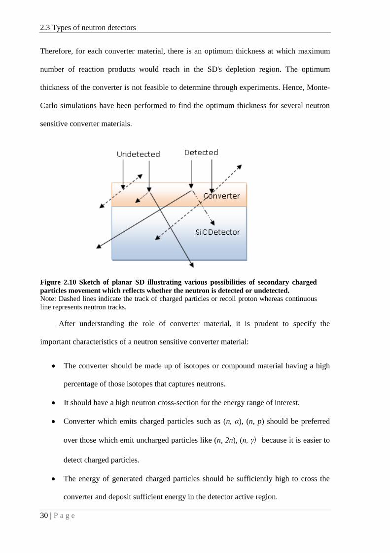
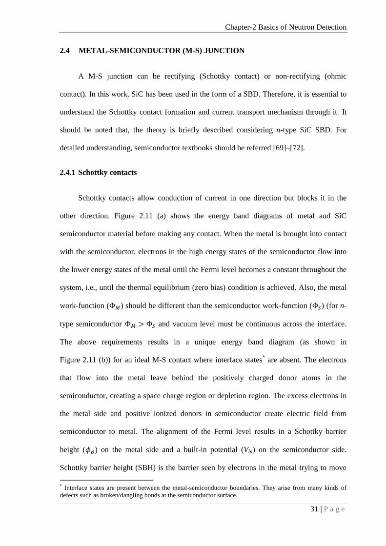
Page 1
STUDY OF SiC-BASED NEUTRON DETECTOR FOR
APPLICATIONS IN THE HARSH ENVIRONMENT
OF FAST REACTORS
By
SHIVANG TRIPATHI
(Enrolment No. ENGG02201304012)
Indira Gandhi Centre for Atomic Research, Kalpakkam
A thesis submitted to the
Board of Studies in Engineering Sciences
In partial fulfillment of requirements
for the Degree of
DOCTOR OF PHILOSOPHY
of
HOMI BHABHA NATIONAL INSTITUTE
May, 2019
Page 3
Homi Bhabha National Institute
Recommendations of the Viva Voce Committee
As members of the Viva Voce Committee, we certify that we have read the dissertation
prepared by Shivang Tripathi entitled "Study of SiC-based neutron detector for
applications in the harsh environment of Fast Reactors" and recommend that it may
be accepted as fulfilling the thesis requirement for the award of Degree of Doctor of
Philosophy.
Chairman - Dr. K. Velusamy Date:
Guide / Convener - Dr. K. Devan Date:
Examiner - Dr. Seema Sharma (IISER, Pune) Date:
Member 1- Dr. B. K. Panigrahi Date:
Member 2- Dr. Anish Kumar Date:
Technology Advisor- Shri. Nagaraj C.P. Date:
Final approval and acceptance of this thesis is contingent upon the candidate‘s
submission of the final copies of the thesis to HBNI.
I/We hereby certify that I/we have read this thesis prepared under my/our
direction and recommend that it may be accepted as fulfilling the thesis requirement.
Date:
Place: IGCAR, Kalpakkam Dr. K. Devan
(Guide)
Page 5
STATEMENT BY AUTHOR
This dissertation has been submitted in partial fulfillment of requirements for an
advanced degree at Homi Bhabha National Institute (HBNI) and is deposited in the
Library to be made available to borrowers under rules of the HBNI.
Brief quotations from this dissertation are allowable without special permission, provided
that accurate acknowledgement of source is made. Requests for permission for extended
quotation from or reproduction of this manuscript in whole or in part may be granted by
the Competent Authority of HBNI when in his or her judgment the proposed use of the
material is in the interests of scholarship. In all other instances, however, permission must
be obtained from the author.
(Shivang Tripathi)
Page 7
DECLARATION
I, hereby declare that the investigation presented in the thesis has been carried out by me.
The work is original and has not been submitted earlier as a whole or in part for a degree /
diploma at this or any other Institution / University.
(Shivang Tripathi)
Page 9
List of Publications arising from the thesis
Journal
1. ―The performance simulation of the LiH-SiC-based Fast Neutron Detector
for harsh environment monitoring using Geant4 and TCAD‖, Shivang
Tripathi, C. Upadhyay, C.P. Nagaraj, A. Venkatesan, K. Devan, Nucl.
Instrum. Methods Phys. Res. A., 2019, 916, 246–256.
2. ―Effect of High energy electron and proton irradiation on the electrical
characteristics of Ni/4H-SiC-based SBD‖, Shivang Tripathi, Chandra
Kant Upadhyay, C.P. Nagaraj, A. Venkatesan, K. Devan, J. Instrum.,
2019, 14, P02002.
3. ―Towards radiation hard converter material for SiC-based fast neutron
detectors‖, Shivang Tripathi, Chandra Kant Upadhyay, C.P. Nagaraj, A.
Venkatesan, K. Devan, J. Instrum., 2018, 13, P05026.
4. ―Investigation of enhancement in planar fast neutron detector efficiency
with the stacked structure using Geant4‖, Shivang Tripathi, Chandra
Kant Upadhyay, C.P. Nagaraj, K. Devan, A. Venkatesan, K.
Madhusoodanan, Nucl. Sci. Tech., 2017, 28, 154.
Manuscript under preparation
1. ―Survey of advancements in fast neutron detection‖, Shivang Tripathi, C.
Upadhyay, C.P. Nagaraj, A. Venkatesan and K. Devan.
Book Chapter
1. ―Investigation of Perylene as a Converter Material for Fast Neutron
Detection and Spectroscopy Using GEANT4 Monte Carlo Simulations‖,
Shivang Tripathi, C. Upadhyay, C.P. Nagaraj, A. Venkatesan, K. Devan,
K. Madhusoodanan, in: A. Konkani, R. Bera, S. Paul (Eds.), Adv. Syst.
Control Autom., Springer Singapore, 2018: pp. 189–197.
Page 10
Conferences
1. ―Effect of gamma-irradiation on the electrical characteristics of SiC-based
FNDs‖, Shivang Tripathi, C. Upadhyay, C.P. Nagaraj, A. Venkatesan, K.
Devan, HBNI RSM-MSENM-2018, IGCAR, Kalpakkam, May 7-9, 2018
(Oral presentation).
2. ―LiH-SiC-based Fast Neutron Detector for harsh environment‖, Shivang
Tripathi, C. Upadhyay, C. P. Nagaraj, K. Devan, A. Venkatesan, B. K.
Panigrahi, IARPIC-2018, HBNI, BARC, Mumbai, Jan 16-20, 2018 (Oral
presentation).
3. ―TCAD assisted analysis of Silicon Carbide based Fast Neutron Detector
for nuclear applications‖, Shivang Tripathi, C. Upadhyay, C. P. Nagaraj,
K. Devan, A. Venkatesan, B. K. Panigrahi, 12th IEEE NMDC, Holiday
Inn Atrium, Singapore, October 2-4, 2017 (Oral presentation).
4. ―Geant4 simulations of semiconductor detectors (SiC) for fast neutron
spectroscopy‖, Shivang Tripathi, C. Upadhyay, C.P. Nagaraj, K. Devan,
K. Madhusoodanan, S. A. V. Satya Murty, INDICON, IEEE, New Delhi,
2015 (Poster presentation).
(Shivang Tripathi)
Page 11
DEDICATED
TO
ALL THE NEUTRONS
Page 13
ACKNOWLEDGEMENTS
I would like to express my sincere gratitude and appreciation to all those who have been
with me during the pursuit of my research and helped me to successfully complete this
thesis. First, I want to express my deepest thanks and appreciation to my parents for their
never-ending supports and kindness. Neither this work, nor any success in my life could
be achieved without their shine of wisdom and warmth of love.
I wish to express my best gratitude and thanks to my advisor, Dr. K. Devan,
Head, Reactor Neutronics Division, Reactor Design Group, IGCAR for his persistent
encouragement, everlasting patience, very caring nature and insightful guidance, which in
all the ways led to the completion of my thesis. I am extremely grateful for having the
privilege to work with him and learn from his expertise.
I sincerely thank my former technology adviser Shri K. Madhusoodanan, former
group director, EIG, IGCAR and present technology adviser Shri C.P. Nagaraj, Head,
Nuclear Instrumentation Section, EIG, IGCAR for valuable guidance and support in
technical as well as in administrative issues.
I would like to acknowledge Shri Chandrakant Upadhyay, SO/E, EIG, IGCAR
for his endless patience, detailed guidance and continued encouragement throughout the
course of preparing for and conducting the research. The joy and enthusiasm he has for
this research was contagious and motivational for me, even during tough times. It was a
pleasure to talk with him about work and life.
I convey my heartiest appreciation to my Doctoral Committee (DC) chairman, Dr.
K. Velusamy, DC members Dr. S. Sivakumar, Dr. B. K. Panigrahi and Dr. Anish
Kumar for their valuable inputs, continuous monitoring of my progress and valuable
support throughout the course of my research.
Page 14
My sincere gratitude to, Dr. A.K. Bhaduri, Director, IGCAR and Dr. S.A.V. Satya
Murty, and Dr. P.R. Vasudeva Rao, former Directors, IGCAR for providing excellent
environment to carry out research work.
I sincerely thank Dr. B. K. Panigrahi, Director, EIG, Dr. M. Sai Baba, former
Dean of students‘ affairs, Dr. Lakshmi Narasimhan, Dr. G. Sasikala, former Dean of
Engineering Sciences, Dr. Anish Kumar, present Dean of Engineering Sciences for their
care and support.
My special thanks to Shri. A.Venkatesan Head ICD, Shri. M. Manimaran Head
PIS, Mrs. K. Kameshwari, Head FHCS, Mrs. Somavathi, Mrs. Varuna, Mrs. Nisha, Mr.
Deendhayalan, Mr. Ananda Kumar, Mr. Pradeesh, Mr. Ankit, Mr. Subramanian, Mr. G.K.
Mishra, Mr. RajKumar, Mr. Balasundaram and all members of ICD for their support and
creating a homely environment at the work place during this period. I also thank Mr.
Jehadeeshan, Mr. Sujith and Computer Division staff for HPC facilities.
I am grateful for the financial support provided by research fellowship scheme
(JRF/SRF/ and partial financial support during extension) from Indira Gandhi Centre for
Atomic Research, Department of Atomic Energy, Govt. of India, for the duration of the
work. I thank HBNI for providing the international travel grant to attend the IEEE
Nanotechnology Materials and Devices Conference (NMDC-2017), held in Singapore.
I endow my special gratitude to Dr. P. Vigneshwara, Post Doctoral Research at
IIT-Madras for his kind help in the TCAD simulations. I specially acknowledge Mr.
Manoj Kumar Parida, SRF, IGCAR for all the technical discussion related to GEANT4
simulations.
Page 15
I endow my special gratitude to my Engineering Sciences batch-mates Dr. Vikas
Kumar, Mr. Nidhin, Mr. Sriram and Dr. V. Sumathi for all the memories beginning from
Training School till now.
It is my pleasure to thank all my friends and seniors Dr. Sravanthi. S, Dr. Chandan
Bhagat, Dr. Sumathi. G, Dr. Prema. S, Dr. Santhosh, Dr. Varun Hassija, Dr. Nilakantha,
Dr. Radhikesh, Dr. Irshad, Dr. Vairavel, Dr. Lakshmanan, Dr. Padmolochan, Mr. Amit
Kumar Mishra, Mr. Revanth, Mr. Sarvajith, Mr. Darpan, Mr. Abhishek, Mr. Balram and
all enclavians including Cricket and Badminton team-mates for making my days at
Kalpakkam very colorful.
I endow my special gratitude to Mr. Shashwat Swain and Mrs. Uma who were
always available on the next door for anything. Their presence never let us feel that we
are away from home.
It has been a great honor for me to work in IGCAR and to be surrounded with
some of the brightest and loving people, I have met. To all, I say Thank you from the
bottom of my heart.
I should also be very grateful to my sister Dr. Shambhavi and brother, Mr. Amar
for their consistent support and understanding. A special mention for my wife, Shivangi,
for her patience and presence whenever I needed.
(Shivang Tripathi)
Page 17
CONTENTS
SYNOPSIS i
LIST OF FIGURES v
LIST OF TABLES xi
LIST OF ABBREVIATIONS xiii
CHAPTER 1: INTRODUCTION 1
1.1 Preamble 1
1.2 Motivation 4
1.3 Silicon Carbide- Literature Survey 6
1.3.1 SiC: salient features and properties 6
1.3.2 SiC as a neutron detector 9
1.4 Objectives and Studies Performed 11
1.5 Organization of the thesis 13
CHAPTER 2: BASICS OF NEUTRON DETECTION 15
2.1 Preamble 15
2.2 Mechanisms of neutron interaction with matter 15
2.2.1 Scattering interaction 16 2.2.2 Absorption interaction 19
2.2.3 Neutron interaction cross-section 20 2.2.4 Charged particle interaction with matter 23
2.3 Types of neutron detectors 24
2.3.1 Gas-filled detectors 24
2.3.2 Scintillation detectors 25
2.3.3 Semiconductor Detectors 26
2.4 Metal-Semiconductor (M-S) Junction 31
2.4.1 Schottky contacts 31 2.4.2 Ohmic contacts 33 2.4.3 Current transport mechanism 34 2.4.4 Current-Voltage (I-V) relationship 35 2.4.5 Capacitance-Voltage (C–V) relationship 36
2.5 Defects in semiconductors 38
2.5.1 Primary Defects 38
2.5.2 Secondary defects 39 2.5.3 Defects in SiC 42 2.5.4 Effects of irradiation induced defects 43
2.6 Summary 44
Page 18
CHAPTER 3: MODELING TOOLS 45
3.1 Preamble 45
3.2 Monte-Carlo (MC) Method 45
3.2.1 Monte-Carlo in Nuclear and Particle Physics 46
3.3 GEANT4 simulation toolkit 47
3.3.1 GEANT4 class categories 48 3.3.2 GEANT4 simulation flow for present work 51 3.3.3 System information where GEANT4 simulations
were performed 55
3.4 Semiconductor device simulation using TCAD 56
3.4.1 Silvaco: TCAD simulation suite 56 3.4.2 Basic Semiconductor Equations 59
3.4.3 Models for SiC device description in TCAD 60 3.4.4 Irradiation-induced defect definition in TCAD 64
3.5 Summary 66
CHAPTER 4: CONVERTER OPTIMIZATION AND EFFICIENCY
ENHANCEMENT 67
4.1 Preamble 67
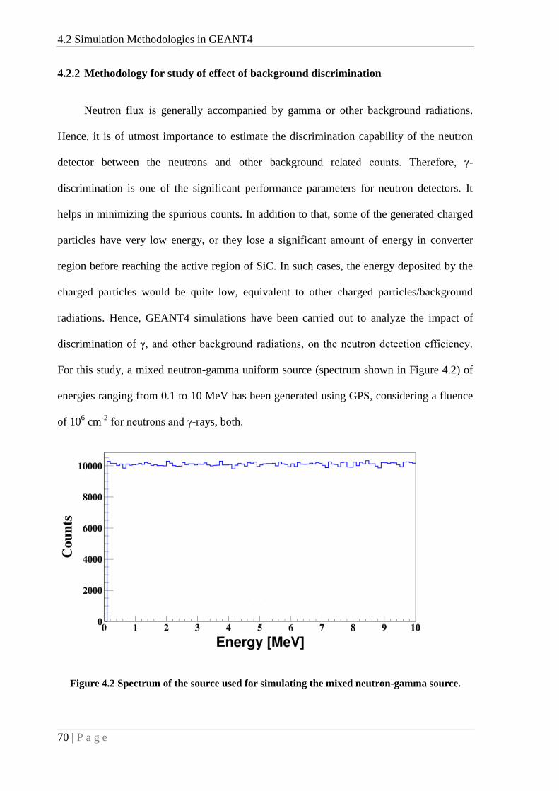
4.2 Simulation Methodologies in GEANT4 68
4.2.1 Methodology for converter thickness optimization 68
4.2.2 Methodology for study of effect of background
discrimination 70 4.2.3 Methodology for study of efficiency improvement 71
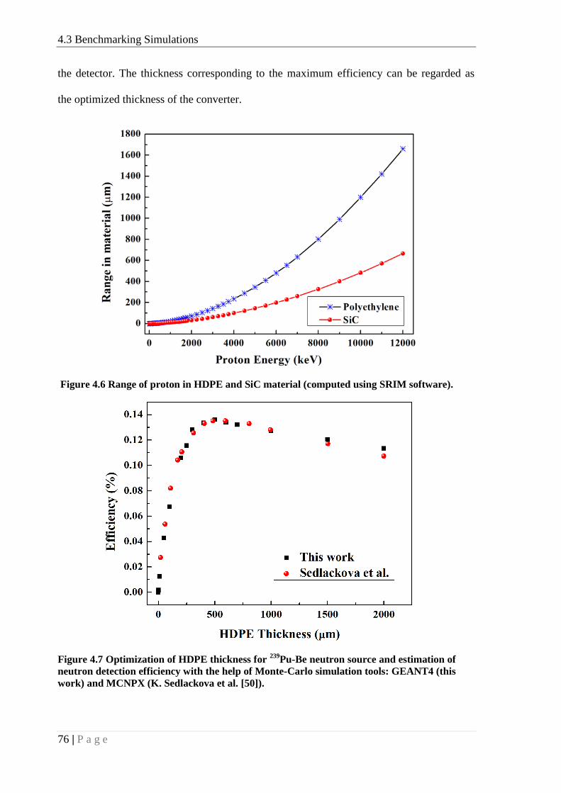
4.3 Benchmarking Simulations 72
4.3.1 Probability of Interaction for 1 MeV neutrons in
HDPE 72 4.3.2 HDPE thickness optimization for
239Pu-Be neutron
source 74 4.3.3 HDPE thickness optimization for 2.5 MeV D-D
neutron source 77
4.4 Simulation Results and Discussions 78
4.4.1 Nuclear reactions in Direct and Indirect conversion
SiC-based detectors 79 4.4.2 HDPE as a converter (HDPE-SiC-based detector) 83 4.4.3 Study of other hydrogenous converters for harsh
environments 90 4.4.4 LiH as a converter (LiH-SiC-based detector) 92
4.4.5 Comparison of Energy deposition in SiC through
LiH & HDPE 99
4.4.6 Perylene as a converter (perylene–SiC-based
detector) 102 4.4.7 Dependence of Efficiency on source distribution 104
4.5 Summary 107
Page 19
CHAPTER 5: EFFECT OF DEEP LEVELS ON THE CHARACTERISTICS
OF SiC-BASED SBDS 109
5.1 Preamble 109
5.2 Device simulation methodology in SILVACO TCAD 110
5.3 Simulation Results & Discussions 113
5.3.1 Characteristics of as-grown (not-irradiated) Ni/4H-
SiC SBD detector 113 5.3.2 Characteristics of Gamma-irradiated (dose=100
Mrad) Ni/4H-SiC SBD detector 115
5.3.3 Characteristics of 8.2 MeV Electron-irradiated
Ni/4H-SiC SBD detector 119 5.3.4 Characteristics of 6.5 MeV proton-irradiated Ni/4H-
SiC SBD detector 122 5.3.5 Characteristics of Neutron-irradiated Ni/4H-SiC
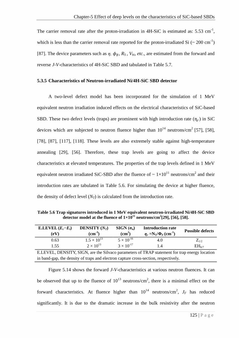
SBD detector 125
5.4 Summary 129
CHAPTER 6: SUMMARY, CONCLUSIONS AND FUTURE DIRECTIONS 131
6.1 Summary & Conclusions 131
6.2 Scope for the future work 136
REFERENCES 137
Page 21
i
SYNOPSIS
Neutron detectors are an inevitable component of a Neutron Flux Monitoring System
(NFMS) in a nuclear power plant. They measure neutron flux at various core locations by
which distinct signals such as absolute power, rate of change of power (period), and
change in reactivity are generated to enable control of the reactor power and also to
initiate safety action on crossing threshold. Hence, the Instrumentation and Control (I&C)
system of a nuclear power plant is necessary to have a reliable and fast acting neutron
flux monitoring system for ensuring its safe operation in all states of operation. The state-
of-the-art gas-filled neutron detectors such as fission chambers, 10
B and BF3 proportional
counters, and 10
B based Compensated Ion Chambers (CICs) are generally deployed for
this purpose.
In the recent past, particularly after Fukushima accident, more emphasis has been given to
core safety in the design of nuclear reactors with the aim of practically eliminating the
core disruptive accidents. For this to happen, I&C system design demands improved
reliability. To meet this objective, more redundant and diverse design of neutron detectors
is essential in the NFMS. In India, developing a miniature detector system which can
withstand harsh-environments with comparable performance of gas-filled detectors is the
need of the day, for usage in future fast reactors. The works carried out towards the
development of such a diverse neutron detector is presented in this thesis. After detailed
and systematic review, a wide band-gap semiconductor, i.e., Silicon Carbide (SiC) has
been chosen for developing a diverse neutron detector for harsh-environments of fast
reactors.
The primary objective of this thesis is to provide the theoretical basis for the optimization
of semiconductor detectors and ensuring the harsh-environment operability before its
costly and time consuming fabrication process.
Page 22
ii
Towards the development of a SiC-based fast neutron detector, the following important
works are carried out and presented in this thesis:
a) Development of a suitable computational model to study the physics of SiC-based
detectors and to perform Monte-Carlo based simulation towards optimization of
converter layer
A planar structure of SiC-based semiconductor neutron detector is modeled using the
Monte-Carlo tool, i.e., GEANT4 (GEometry ANd Tracking). It‘s benchmarking and
validation has been carried out with the published results. The performance of several
hydrogenous converter materials has been studied in the harsh-environments of Fast
Breeder Reactors (FBRs) by juxtaposing with SiC detector. This study provides the
optimization of several converter materials for different energy neutron sources and
the corresponding efficiency offered by SiC-based detectors.
b) Study for improving the detector performance in terms of background
discrimination and efficiency
One of the major issues with the neutron detectors is the spurious counts from the
background irradiation such as γ-rays. This study involves the discrimination of the
background radiations and its effect on the neutron detection efficiency. Furthermore,
it is desirable to achieve efficiency equivalent to or better than gas-filled detectors.
c) Device simulation and assessing the system performance in harsh environments
This work involves the modeling of the SiC-based Schottky Barrier Diode (SBD) in
the device simulation tool, i.e., Technology Computer-Aided Design (TCAD) from
SilvacoTM
, and its validation with the literature. Further work involves introducing
deep-levels due to gamma, proton, electron, and neutron irradiations, and studying its
Page 23
iii
effect on the device characteristics to predict the degradation with respect to increasing
radiation fluence.
In summary, a novel LiH-SiC-based stacked neutron detector has been optimized and the
effects of irradiation on the SiC device characteristics have been assessed for its
applications in the harsh environment of fast reactors.
Page 25
v
LIST OF FIGURES
Figure 1.1 Tetrahedral bonding of (a) Si-atom with the four nearest C-atoms, and
(b) C-atom with the four nearest Si-atoms [22] 7
Figure 2.1 Types of neutron interactions with materials. 16
Figure 2.2 Neutron elastic scattering interaction diagram. 18
Figure 2.3 Total neutron cross–sections for 3He,
6Li, and
10B isotopes [58]. 22
Figure 2.4 Schematic diagram of a typical Gas-filled detector. 25
Figure 2.5 Schematic diagram of a scintillation detector with PMT setup [60]. 26
Figure 2.6 Schematic of a semiconductor diode detector. 27
Figure 2.7 Schematic of detector electronics. 27
Figure 2.8 Representation of (a) Direct (b) Indirect-Conversion Neutron
Detectors. 28
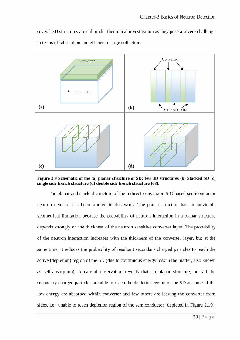
Figure 2.9 Schematic of the (a) planar structure of SD; few 3D structures (b)
Stacked SD (c) single side trench structure (d) double side trench
structure [64]. 29
Figure 2.10 Sketch of planar SD illustrating various possibilities of secondary
charged particles movement which reflects whether the neutron is
detected or undetected. 30
Figure 2.11 Energy band diagram of metal n-type semiconductor contact with ΦM
> ΦS. 32
Figure 2.12 Basic current transport mechanisms across the M-S junction. 35
Figure 2.13 The schematic diagram of point defects in semiconductors, taken
from [72]. 39
Figure 2.14 The schematic diagram of different carrier transitions between deep-
levels and the energy bands. 41
Figure 3.1 An illustration of the GEANT4 process flow. 54
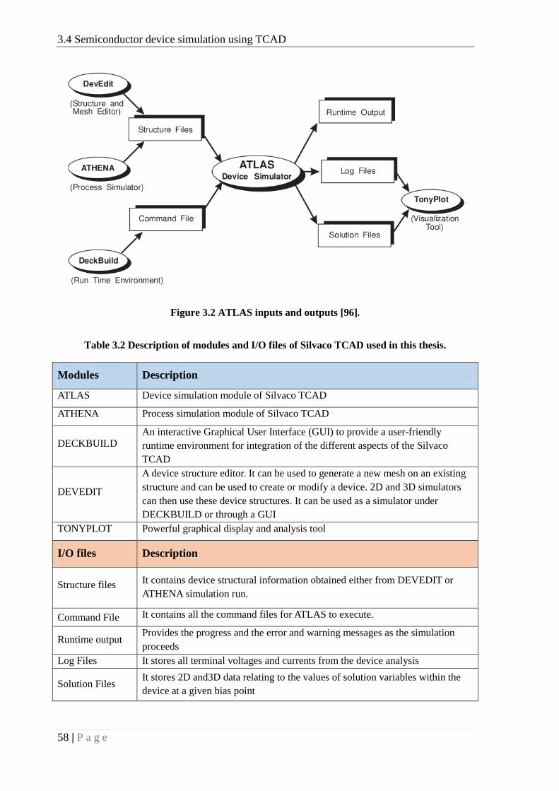
Figure 3.2 ATLAS inputs and outputs [92]. 58
Figure 3.3 Simulated reverse J-V-characteristics of Ni/4H-SiC SBD with and
without the barrier lowering and tunneling models. 63
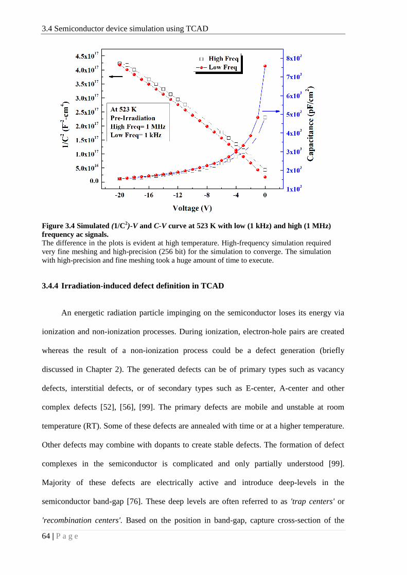
Figure 3.4 Simulated (1/C2)-V and C-V curve at 523 K with low (1 kHz) and high
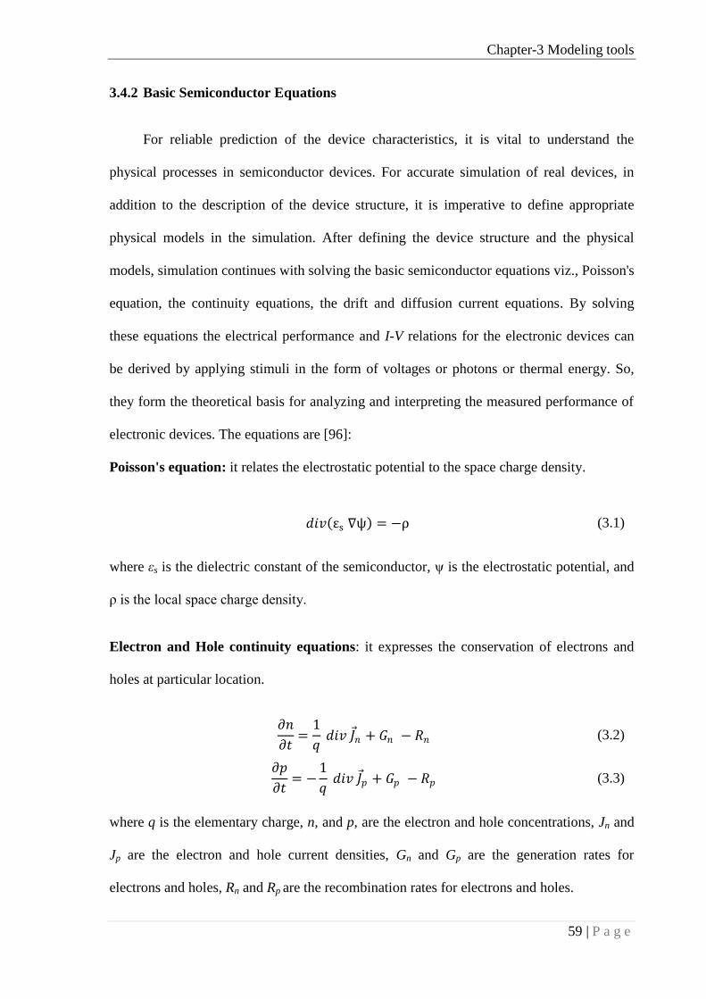
(1 MHz) frequency ac signals. 64
Page 26
vi
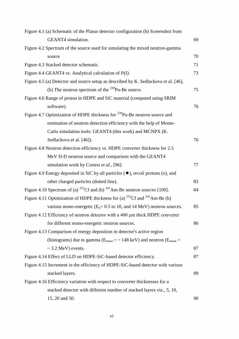
Figure 4.1 (a) Schematic of the Planar detector configuration (b) Screenshot from
GEANT4 simulation. 69
Figure 4.2 Spectrum of the source used for simulating the mixed neutron-gamma
source 70
Figure 4.3 Stacked detector schematic. 71
Figure 4.4 GEANT4 vs. Analytical calculation of P(I). 73
Figure 4.5 (a) Detector and source setup as described by K. Sedlackova et al. [46],
(b) The neutron spectrum of the 239
Pu-Be source. 75
Figure 4.6 Range of proton in HDPE and SiC material (computed using SRIM
software). 76
Figure 4.7 Optimization of HDPE thickness for 239
Pu-Be neutron source and
estimation of neutron detection efficiency with the help of Monte-
Carlo simulation tools: GEANT4 (this work) and MCNPX (K.
Sedlackova et al. [46]). 76
Figure 4.8 Neutron detection efficiency vs. HDPE converter thickness for 2.5
MeV D-D neutron source and comparison with the GEANT4
simulation work by Cortesi et al., [96]. 77
Figure 4.9 Energy deposited in SiC by all particles (), recoil protons (o), and
other charged particles (dotted line). 83
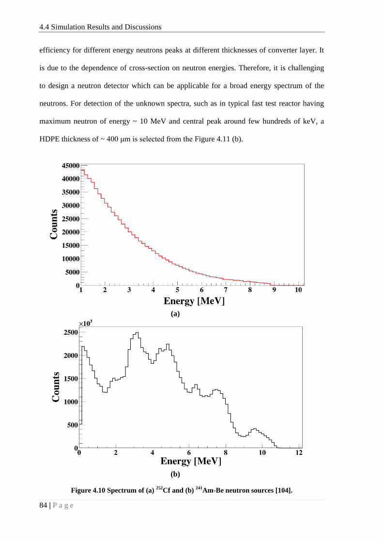
Figure 4.10 Spectrum of (a) 252
Cf and (b) 241
Am-Be neutron sources [100]. 84
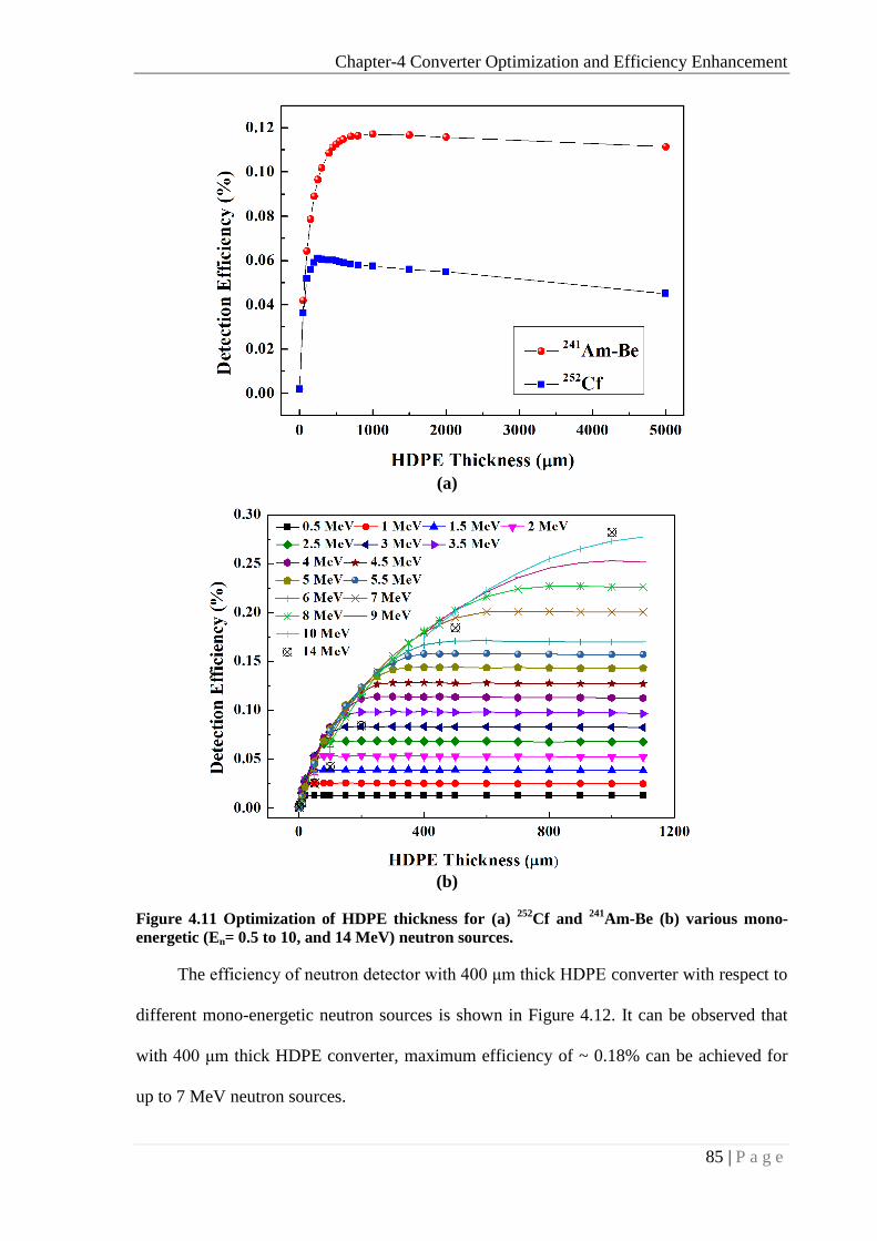
Figure 4.11 Optimization of HDPE thickness for (a) 252
Cf and 241
Am-Be (b)
various mono-energetic (En= 0.5 to 10, and 14 MeV) neutron sources. 85
Figure 4.12 Efficiency of neutron detector with a 400 μm thick HDPE converter
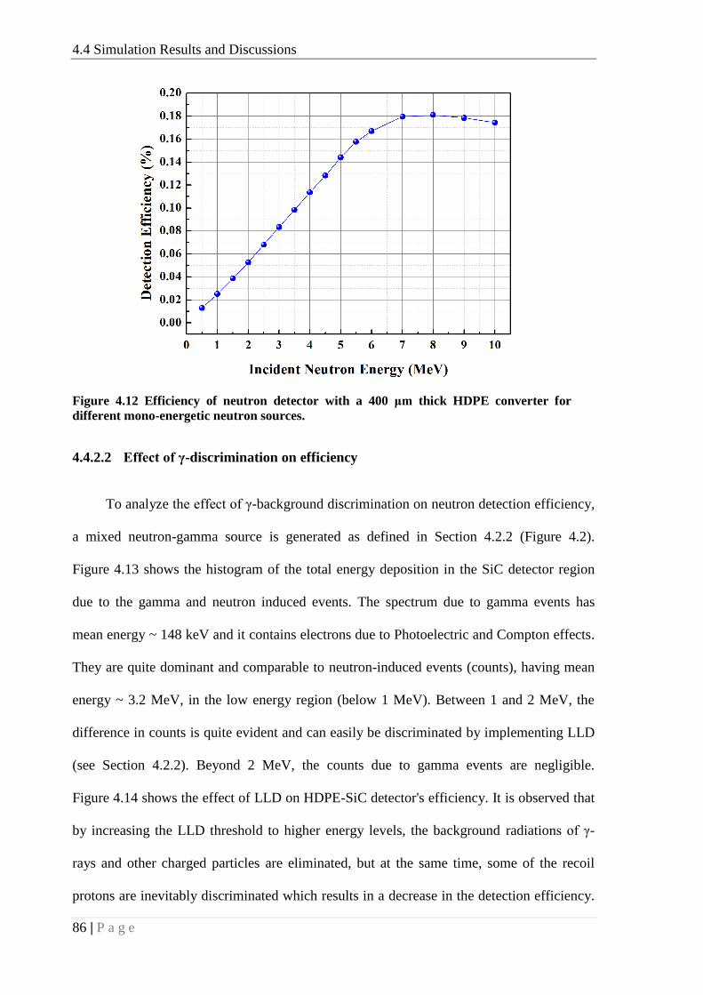
for different mono-energetic neutron sources. 86
Figure 4.13 Comparison of energy deposition in detector's active region
(histograms) due to gamma (Emean = ~ 148 keV) and neutron (Emean =
~ 3.2 MeV) events. 87
Figure 4.14 Effect of LLD on HDPE-SiC-based detector efficiency. 87
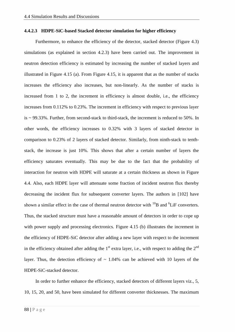
Figure 4.15 Increment in the efficiency of HDPE-SiC-based detector with various
stacked layers. 89
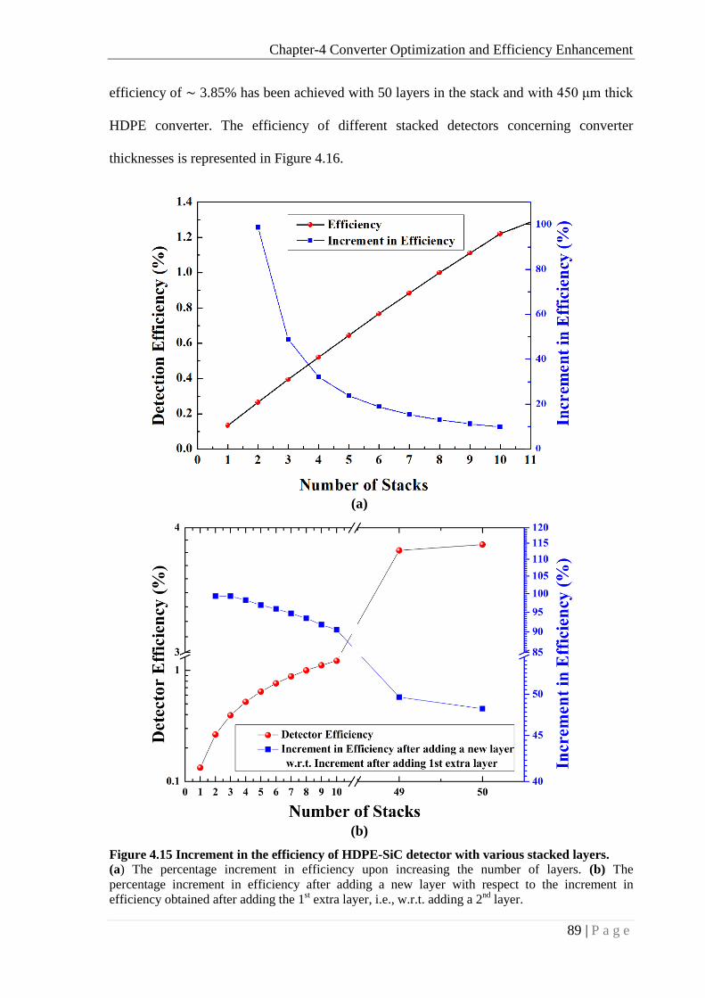
Figure 4.16 Efficiency variation with respect to converter thicknesses for a
stacked detector with different number of stacked layers viz., 5, 10,
15, 20 and 50. 90
Page 27
vii
Figure 4.17 Comparison of detection efficiency offered by selected converter
materials. 92
Figure 4.18 Range of protons and 7Li ion in LiH converter material (calculated
using SRIM package). 94
Figure 4.19 Efficiency vs. LiH thickness for different mono-energetic neutron
sources. 95
Figure 4.20 Efficiency vs. LiH thickness for 241
Am-Be neutron source. 95
Figure 4.21 Comparison of energy deposition (histograms) in the detector active
region due to gamma (Emean = ~ 150 keV) and neutron (Emean = ~ 3.5
MeV) events. 97
Figure 4.22 Effect of various LLD threshold values on the neutron detection
efficiency of the LiH-SiC-based detector. 98
Figure 4.23 Increment in the detection efficiency of LiH-SiC-based detector with
various stacked layers. 100
Figure 4.24 Efficiency variation with respect to converter thicknesses for a
stacked detector with a different number of stacked layers viz., 5, 10,
15, 20 and 50. 101
Figure 4.25 The histogram of the total energy deposited in the active region of
SiC by the secondary charged particles generated due to the neutron
interaction in the HDPE and LiH converters. 101
Figure 4.26 The histogram of energy deposition by the recoil-protons (generated
in LiH and HDPE) in SiC active region. 102
Figure 4.27 Efficiency versus perylene thickness for various mono-energetic
neutrons. 104
Figure 4.28 Perylene thickness optimization for 241
Am-Be Neutron source. 105
Figure 4.29 GEANT4 simulation in Real World Scenario. 106
Figure 4.30 Efficiency vs. LiH converter thickness of LiH-SiC-based FND for
planar and multiple sources 106
Figure 5.1 (a) Schematic of n-type 4H-SiC 2D-structure simulated in TCAD (b)
2D-structure generated in DEVEDIT module. 110
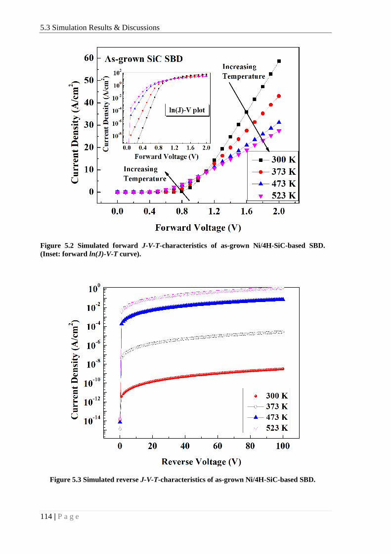
Figure 5.2 Simulated forward J-V-T-characteristics of as-grown Ni/4H-SiC-based
SBD. (Inset: forward ln(J)-V-T curve). 114
Figure 5.3 Simulated reverse J-V-T-characteristics of as-grown Ni/4H-SiC-based
SBD. 114
Page 28
viii
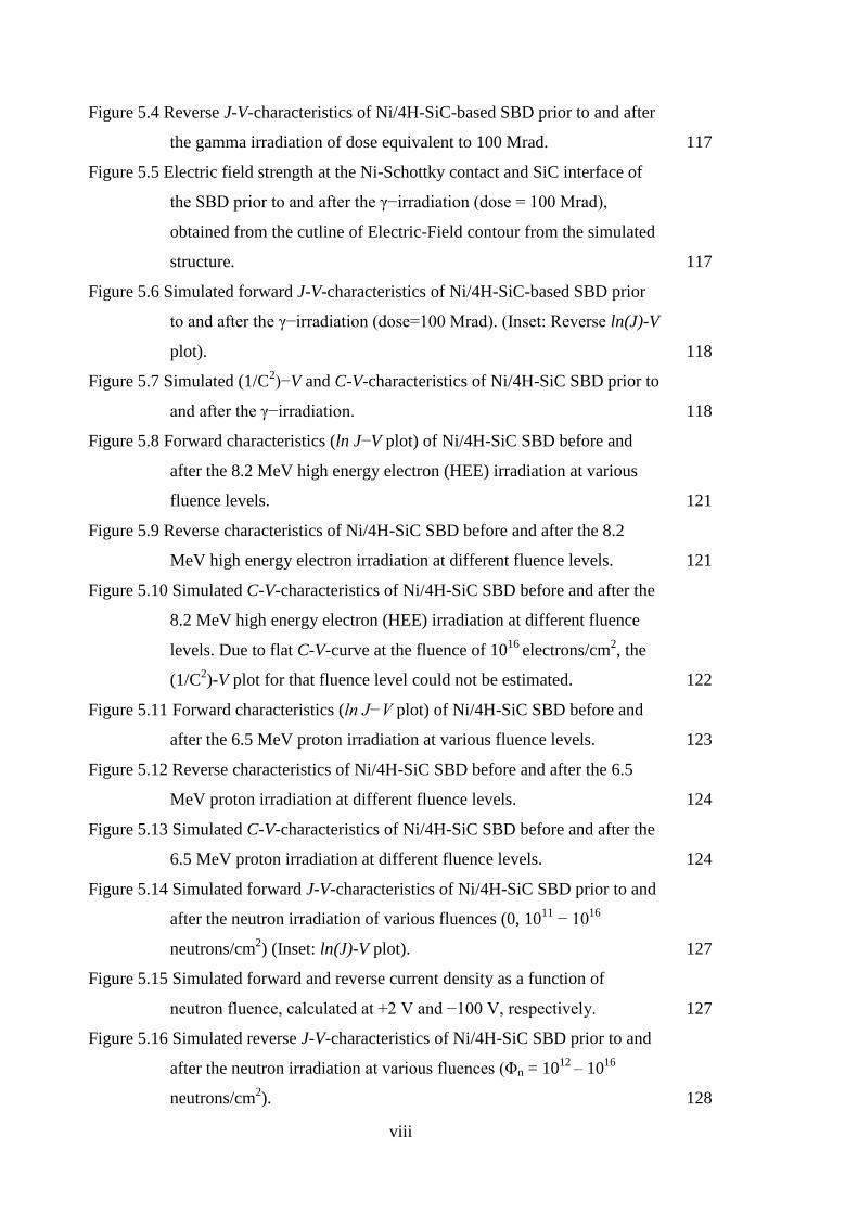
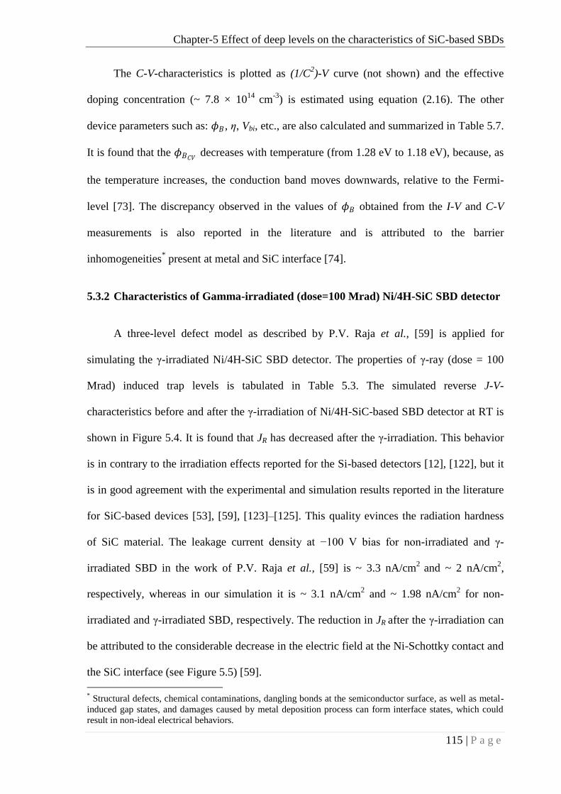
Figure 5.4 Reverse J-V-characteristics of Ni/4H-SiC-based SBD prior to and after
the gamma irradiation of dose equivalent to 100 Mrad. 117
Figure 5.5 Electric field strength at the Ni-Schottky contact and SiC interface of
the SBD prior to and after the γ−irradiation (dose = 100 Mrad),
obtained from the cutline of Electric-Field contour from the simulated
structure. 117
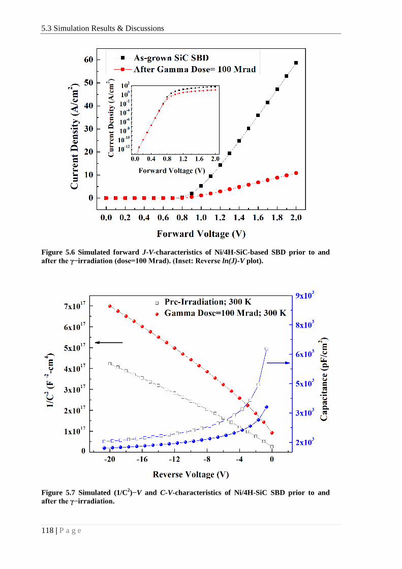
Figure 5.6 Simulated forward J-V-characteristics of Ni/4H-SiC-based SBD prior
to and after the γ−irradiation (dose=100 Mrad). (Inset: Reverse ln(J)-V
plot). 118
Figure 5.7 Simulated (1/C2)−V and C-V-characteristics of Ni/4H-SiC SBD prior to
and after the γ−irradiation. 118
Figure 5.8 Forward characteristics (ln J−V plot) of Ni/4H-SiC SBD before and
after the 8.2 MeV high energy electron (HEE) irradiation at various
fluence levels. 121
Figure 5.9 Reverse characteristics of Ni/4H-SiC SBD before and after the 8.2
MeV high energy electron irradiation at different fluence levels. 121
Figure 5.10 Simulated C-V-characteristics of Ni/4H-SiC SBD before and after the
8.2 MeV high energy electron (HEE) irradiation at different fluence
levels. Due to flat C-V-curve at the fluence of 1016
electrons/cm2, the
(1/C2)-V plot for that fluence level could not be estimated. 122
Figure 5.11 Forward characteristics (ln J−V plot) of Ni/4H-SiC SBD before and
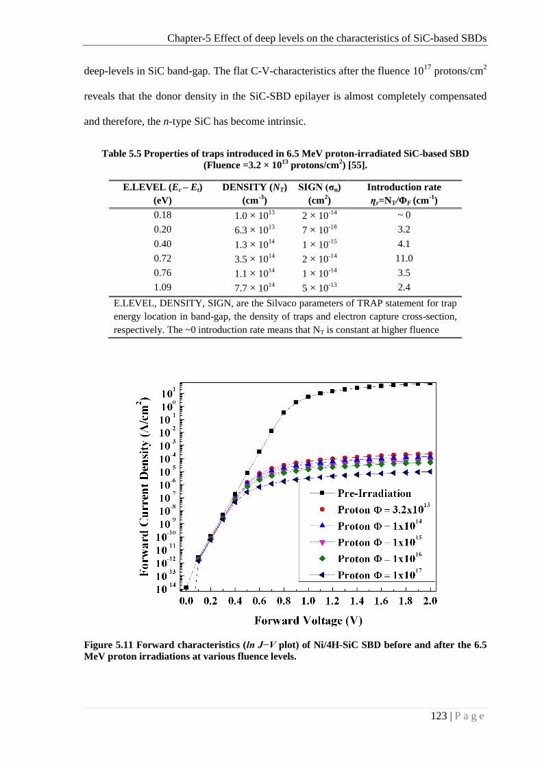
after the 6.5 MeV proton irradiation at various fluence levels. 123
Figure 5.12 Reverse characteristics of Ni/4H-SiC SBD before and after the 6.5
MeV proton irradiation at different fluence levels. 124
Figure 5.13 Simulated C-V-characteristics of Ni/4H-SiC SBD before and after the
6.5 MeV proton irradiation at different fluence levels. 124
Figure 5.14 Simulated forward J-V-characteristics of Ni/4H-SiC SBD prior to and
after the neutron irradiation of various fluences (0, 1011
− 1016
neutrons/cm2) (Inset: ln(J)-V plot). 127
Figure 5.15 Simulated forward and reverse current density as a function of
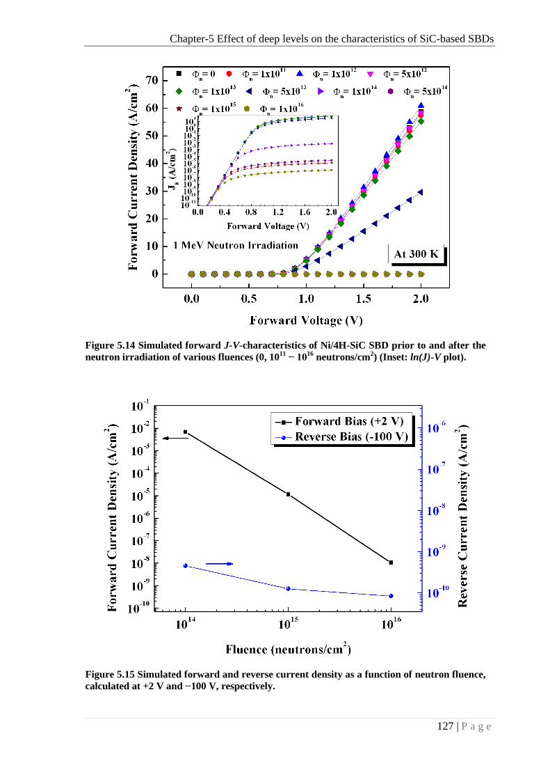
neutron fluence, calculated at +2 V and −100 V, respectively. 127
Figure 5.16 Simulated reverse J-V-characteristics of Ni/4H-SiC SBD prior to and
after the neutron irradiation at various fluences (Φn = 1012
– 1016
neutrons/cm2). 128
Page 29
ix
Figure 5.17 Simulated (1/C2)-V and C-V-characteristics of Ni/4H-SiC SBD prior
to and after the neutron−irradiation of various fluences. 128
Figure 5.18 Breakdown simulation of Ni/4H-SiC SBD before and after the
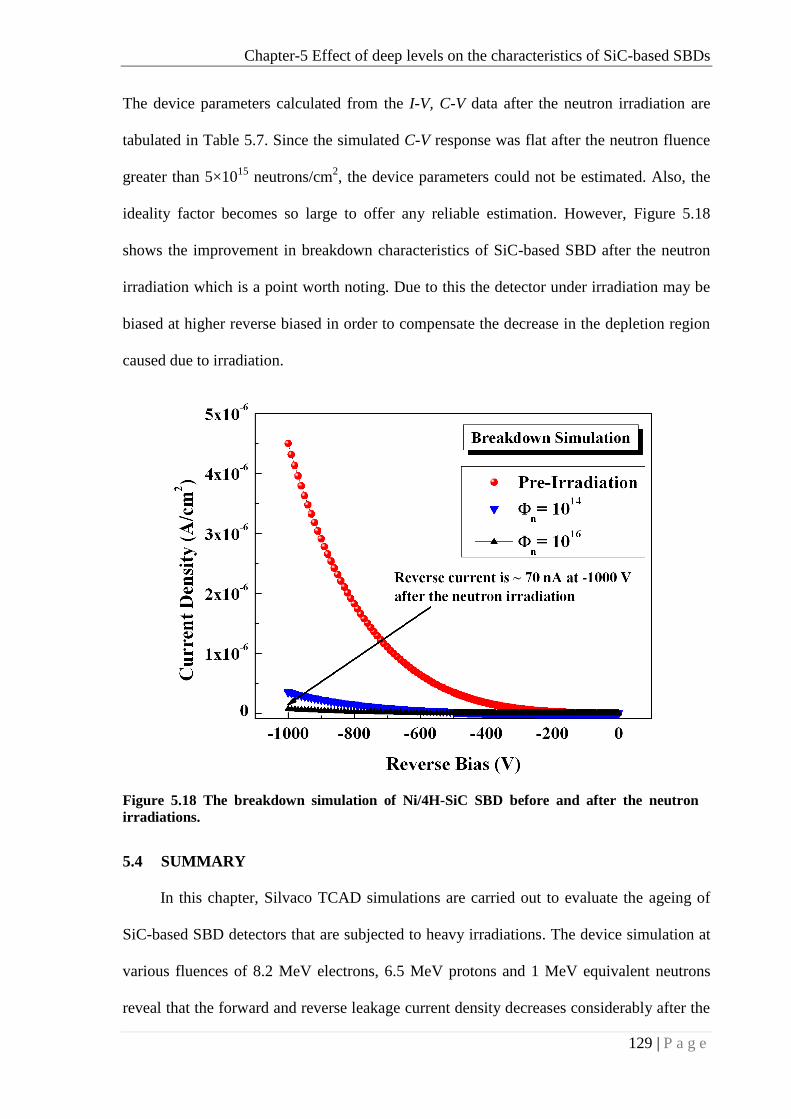
neutron irradiations. 129
Page 31
xi
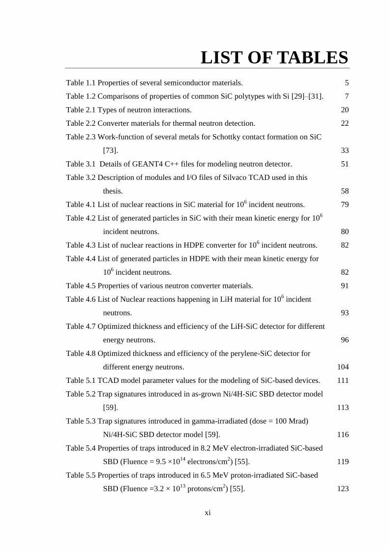
LIST OF TABLES
Table 1.1 Properties of several semiconductor materials. 5
Table 1.2 Comparisons of properties of common SiC polytypes with Si [29]–[31]. 7
Table 2.1 Types of neutron interactions. 20
Table 2.2 Converter materials for thermal neutron detection. 22
Table 2.3 Work-function of several metals for Schottky contact formation on SiC
[73]. 33
Table 3.1 Details of GEANT4 C++ files for modeling neutron detector. 51
Table 3.2 Description of modules and I/O files of Silvaco TCAD used in this
thesis. 58
Table 4.1 List of nuclear reactions in SiC material for 106 incident neutrons. 79
Table 4.2 List of generated particles in SiC with their mean kinetic energy for 106
incident neutrons. 80
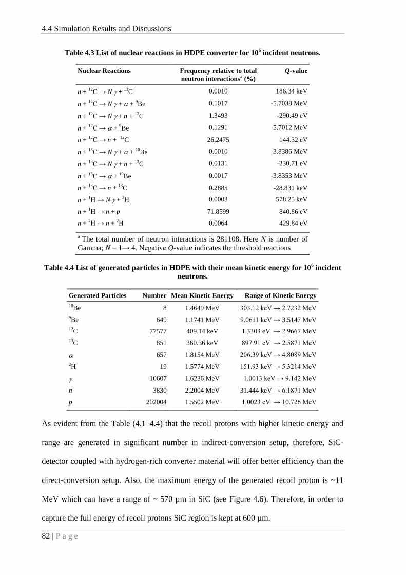
Table 4.3 List of nuclear reactions in HDPE converter for 106 incident neutrons. 82
Table 4.4 List of generated particles in HDPE with their mean kinetic energy for
106 incident neutrons. 82
Table 4.5 Properties of various neutron converter materials. 91
Table 4.6 List of Nuclear reactions happening in LiH material for 106 incident
neutrons. 93
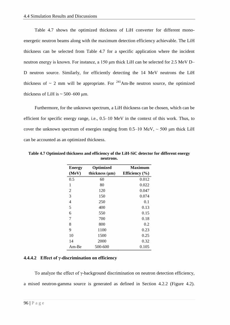
Table 4.7 Optimized thickness and efficiency of the LiH-SiC detector for different
energy neutrons. 96
Table 4.8 Optimized thickness and efficiency of the perylene-SiC detector for
different energy neutrons. 104
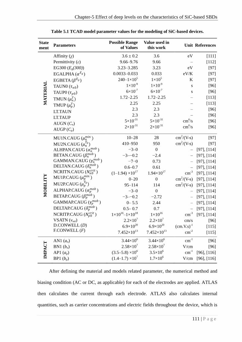
Table 5.1 TCAD model parameter values for the modeling of SiC-based devices. 111
Table 5.2 Trap signatures introduced in as-grown Ni/4H-SiC SBD detector model
[59]. 113
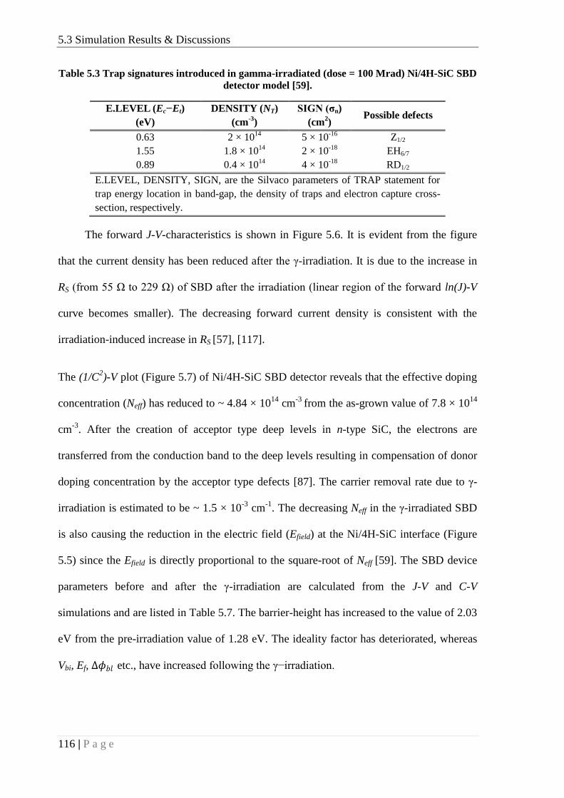
Table 5.3 Trap signatures introduced in gamma-irradiated (dose = 100 Mrad)
Ni/4H-SiC SBD detector model [59]. 116
Table 5.4 Properties of traps introduced in 8.2 MeV electron-irradiated SiC-based
SBD (Fluence = 9.5 ×10¹⁴
electrons/cm2) [55]. 119
Table 5.5 Properties of traps introduced in 6.5 MeV proton-irradiated SiC-based
SBD (Fluence =3.2 × 10¹³
protons/cm2) [55]. 123
Page 32
xii
Table 5.6 Trap signatures introduced in 1 MeV equivalent neutron-irradiated
Ni/4H-SiC SBD detector model at the fluence of 1×10¹¹
neutrons/cm2[29], [56], [58]. 125
Table 5.7 Device parameters determined from the I-V & C-V simulations of the
Ni/4H-SiC SBD. 130
Page 33
xiii
LIST OF ABBREVIATIONS
FBRs Fast Breeder Reactor
FNDs Fast Neutron Detectors
GEANT4 Geometry And Tracking (A Monte-Carlo based code)
GPS General Particle Source
HDPE High Density Polyethylene
I&C Instrumentation and Control
K.E. Kinetic Energy
keV Kilo-Electron Volts
LiH Lithium Hydride
LLD Low Level Discriminator
meV Milli-Electron Volts
MeV Mega-Electron Volts
M-S Metal-Semiconductor junction
MW Mega Watts
NFMS Neutron Flux Monitoring System
NIEL Non-Ionizing Energy Loss
PDF Probability Distribution Function
SBDs Schottky Barrier Diodes
SBH Schottky Barrier Height
SiC Silicon Carbide
SDs Semiconductor Detectors
TCAD Technology Computer-Aided Design
TE Thermionic Emission
Page 35
Chapter-1 Introduction
1 | P a g e
1 INTRODUCTION
1.1 PREAMBLE
The neutron is a subatomic neutral particle which makes it pivotal for a variety of
applications. For instance, neutrons play key role in neutron scattering experiments for
studying the different physical properties of materials [1]; in Neutron Activation Analysis
for determining the concentrations of elements [2]; in neutron capture therapy for treating
the cancer patients [3]; in neutron tomography for 3D-imaging [4]; and another important
application is in the nuclear reactors where neutrons are responsible for sustaining fission
chain reaction [5]. All these applications require an indispensable sensor, generally referred
as ―Neutron Detectors‖ to detect or count the presence of neutrons. The zero electric
charge, empowers neutrons to penetrate deeper and traverse considerable distance in the
medium without undergoing any interaction, hence without being detected. Additionally,
unlike charged particles (e.g., α, proton, heavy ions), neutrons do not ionize the atoms
directly. Therefore, their detection is quite challenging and rely on the measurement of
secondary charged particles that are generated as a result of complex nuclear (neutron-
nucleus) reactions [6].
In nuclear applications, neutron detectors are the most crucial components in Neutron
Flux Monitoring System (NFMS). They measure neutron flux (Φ), i.e., number of
neutrons/cm2/s, at various core locations. The neutron flux in a reactor is approximately
expressed by Equation (1.1) [7]:
Page 36
1.1 Preamble
2 | P a g e
𝛷 = 3.125 × 10¹² ×
𝑃 (MW)
Σ𝑓
(1.1)
where Σ𝑓 is the macroscopic cross-section (cm-1
) for the fission reaction in the reactor core.
The reactor power (megawatts) is proportional to the neutron flux. It is apparent that for
control and monitoring of the nuclear reactor, the information regarding the neutron
population is exceptionally essential. Based on the neutron flux information, the NFMS
generates various signals such as absolute power, rate of change of power (period), change
in reactivity, etc., to enable control of the reactor power, and also initiate safety action on
crossing their threshold values. Hence, Instrumentation and Control (I&C) system of a
nuclear power plant is necessary to have a reliable and fast acting neutron flux monitoring
system for ensuring its safety for all the states of operation, i.e., start-up, intermediate and
power ranges, shutdown, fuel handling, and during all design basis events [8].
Neutron detectors are broadly categorized as gas-filled detectors, scintillators, and
thin-film-coated semiconductor diodes, elucidated in Chapter 2. For nuclear applications,
state-of-the-art gas-filled neutron detectors such as fission chambers, 10
B and BF3
proportional counters, and 10
B based Compensated Ion Chambers (CICs) are generally
deployed. In gas-filled detectors, the incident neutrons interact with the neutron sensitive
material coated on the inner wall of a gas-filled chamber and generate secondary charged
particles (e.g., α-particles or highly charged fission fragments) which initiate ionization
or/and excitation in the filled gas. The electron-ion pairs generated in this process are
collected on the electrodes by applying a high voltage supply. The corresponding electrical
signal indicates the presence of neutrons. The limitations of these gas-filled detectors
include large dimension, requirement of high voltage supply and need of pure gas for their
efficient operation. Additionally, they require relatively high energy (~ 25–30 eV) to create
Page 37
Chapter-1 Introduction
3 | P a g e
electron-ion pairs in the filled gas which results in a reduced number of charge pairs and
eventually low output signal [9].
In medium sized sodium cooled pool type Fast Breeder Reactors (FBRs) [10], [11],
since the core is designed not in the most reactive configuration, the online reactivity
monitoring is generally adapted to detect and initiate safety action at the incipient stage
itself even for small changes in the core state. It is very challenging to have a single
detector system to monitor neutron flux over ten orders of magnitude, spanning shutdown
to full power, particularly in a pool type reactor such as the Indian 500 MWe sodium
cooled pool type Prototype Fast Breeder Reactor (PFBR) [8]. Due to the provision of thick
radial and axial shielding in the design to protect the reactor core components, the neutron
flux is highly attenuated at the ex-core, and ex-vessel detector locations. Hence,
combination of different detectors (for different states of operation) working in different
modes (pulse mode, Campbell mode and pulse mode with linear count rate meters) are
deployed at both in-vessel and out-vessel locations [8]. The presence of harsh environments
such as high temperature (~ 500 ˚C), high gamma dose (100 Mrad), and high neutron fluxes
(~ 1015
n/cm2/s) within the vessel and very low neutron flux at ex-vessel locations, dictates
the designing aspects of the high-temperature fission chambers (HTFCs) [8]. The
challenges involved in the designing of HTFC detectors are:
Unavailability of enriched uranium to achieve higher sensitivities.
Disintegration of uranium coating due to thermal shocks.
Chemical cleaning of the gas is required to the extent of parts per billion (ppb) levels.
Welding/brazing joints, metal-ceramic seals must withstand high pressure and
temperature fluctuations.
Increase in the leakage currents due to decrease in the insulation resistance of ceramic
materials in the vessel at high temperature.
Page 38
1.2 Motivation
4 | P a g e
1.2 MOTIVATION
In the recent past, particularly after the Fukushima accident, the core safety aspect in
designing of nuclear reactors has gained a revised emphasis and increased attention, with an
aim of practically eliminating the core disruptive accidents. For this to happen, I&C system
design demands improved reliability. To meet this objective, redundant and diverse design
of neutron detectors is essential in the neutron flux monitoring system. Redundant gas-
filled detectors are already deployed for this purpose. The common mode of failures can
further be minimized through implementation of diverse detectors in the system. Hence,
developing a miniature detector system which can withstand harsh-environments with
comparable performance of gas-filled detectors is the need of the day, for usage in future
indigenous fast reactors. Feasibility studies carried out towards the development of such a
diverse neutron detector is presented in this thesis.
Neutron detection techniques other than gas-filled detectors have to be considered for
implementing the diversity factor. The alternatives could be scintillators or semiconductor-
based detectors. The scintillators are not considered for this study as they cease to
withstand the harsh-environment of fast reactors and are poor in terms of gamma-
discrimination. They also require heavy and delicate Photo Multiplier Tubes for their
operation. On the other hand, semiconductor detectors (SDs) have inherent advantages such
as the requirement of low power for its operation, mass production can lead to cost
reduction, and compact size eases the handling and installation of the detector. Most
importantly, they require relatively lower energy ~ 3–10 eV per electron-hole pair created,
which results in a large number of charge carriers and eventually better signal and resultant
high energy resolution. High mobility of electrons and a smaller area to cover, further,
enhances the charge-collection, counting rate, and much improved signal to noise ration of
the SDs. However, devices based on conventional semiconductors such as Si and Ge are
Page 39
Chapter-1 Introduction
5 | P a g e
unable to withstand high temperature due to their low band-gap, and are also quite prone to
radiation induced damages [12], [13]. Hence, conventional semiconductor-based detectors
are limited to low temperature (< 300 K) applications having adequate cooling provisions
[14], [15]. The high doses of radiation causing the following effects: a) increases the
leakage current which leads to device failure, b) decreases the depletion width which results
in higher dark currents c) changes the effective doping concentration which eventually
leads to type inversion, d) affects the charge collection properties of the device which
degrades the detection efficiency, etc. These limitations of Si-based devices have motivated
the evolution of radiation hard semiconductor devices based on wide band-gap
semiconductor materials such as Silicon Carbide (SiC), Aluminum Nitride (AlN), Boron
Nitride (BN), Gallium Arsenide (GaAs) and Gallium Nitride (GaN) [16]–[20]. Their wider
band-gaps make them suitable for operating in harsh environments. Table 1.1 shows the
properties of several semiconductor materials.
Table 1.1 Properties of several semiconductor materials.
Properties Si Ge GaAs 4H-SiC Diamond GaN Cd(Zn)Te
Atomic Number (Z) 14 32 31/33 14/6 6 31/7 48/52
Band-gap Eg (eV) 1.12 0.67 1.43 3.25 5.5 3.39 1.4-1.6
Density (g-cm-3
) 2.33 5.323 5.3 3.23 3.5 5.3 5.9
e-h pair creation energy (eV) 3.6 2.96 4.3 7.8 13 8.9 4.4
Electron mobility (cm2 /V-s) 1450 3900 8500 1000 1800 440 1100
Hole mobility (cm2 /V-s) 450 1900 400 115 1200 200 100
Electron lifetime (s) >10-3 >10
-3 10-8 5×10
-7 > 10-6 10
-9 10-6
Melting point (℃) 1412 938 1238 2827 3500 3200 1092
Dielectric constant 11.7 16 12.8 9.7 5.5 8.9 10.9
Displacement threshold (eV) 13 20 10 21.8 43 19.5 -
Breakdown voltage,
(MV/cm) 0.5 0.1 0.4 4 10 5 -
Page 40
1.3 Silicon Carbide- Literature Survey
6 | P a g e
In particular, SiC, with a wide band-gap of ~ 3.25 eV and displacement threshold*
energy of 21.8 eV [16], [21], has shown great potential to become a future material of
choice for harsh environment radiation detectors. Si and C atoms in SiC can directly
undergo elastic and inelastic scattering reactions, discussed in Chapter 2, upon interaction
with fast neutrons [22], [23]. In addition to that, a layer of neutron sensitive hydrogenous
converter material (for which fast neutrons have relatively high cross-section for elastic
scattering interaction) can further enhance the detection efficiency [24], [25]. Thus, neutron
detectors of both configurations viz., direct and indirect (discussed in section 2.3.3), can be
built using SiC.
1.3 SILICON CARBIDE- LITERATURE SURVEY
1.3.1 SiC: salient features and properties
SiC is an indirect and wide band-gap compound semiconductor material with a rigid
stoichiometry of 50% silicon (Si) and 50% of carbon (C). Both Si and C atoms are
tetravalent elements which contain four valence electrons in their outermost shells. A
carbon atom is tetrahedrally bonded with covalent bonds to four neighboring atoms of
silicon that are placed in the corner and vice-versa as shown in Figure 1.1 [26]. The bond
length between Si and C atoms is ~ 1.89 Å, whereas, between two atoms of the same
species (Si–Si or C–C), it is ~ 3.08 Å [27], [28].
One property that makes SiC a compelling and distinctive semiconductor is its ability
to form several crystallographic configurations called polytypes. The polytypism is the
phenomenon where material can adopt different crystal structures which vary in one
dimension (i.e., in stacking sequence) without changes in chemical composition [29].
* Minimum kinetic energy that an atom in solid needs to get permanently displaced from its lattice site to
defect position.
Page 41
Chapter-1 Introduction
7 | P a g e
(a) (b)
Figure 1.1 Tetrahedral bonding of (a) Si-atom with the four nearest C-atoms, and (b) C-atom
with the four nearest Si-atoms [26]
The polytypism is the main characteristic of SiC that makes it challenging to study. For
SiC, more than 200 different types of polytypes are known. They have distinct physical,
electrical, and optical properties. It is owing to this reason; some polytypes are preferred
over others. To this date, the 4H-, 6H- and 3C- polytypes of SiC have been most
extensively studied and are being widely used in the electronics industry [27], [29]. The
names of different polytypes are assigned as per Ramsdell Notation: ‹number› ‹letter›;
where the number indicates the number of layers before the sequence repeats and the letter
denotes the crystal structure. For example, 4H-SiC means four different layers are repeated
throughout the material, and the structure is hexagonal. Table 1.2 provides a comparison of
the electrical properties of these common SiC polytypes with Si.
Table 1.2 Comparisons of properties of common SiC polytypes with Si [29]–[31].
Properties 4H-SiC 6H-SiC 3C-SiC Si
Band-gap (eV) (300K) 3.26 3.02 2.36 1.12
Relative dielectric constant 9.7 9.7 9.3 11.9
Breakdown field (MV/cm) 3.0 3.2 >1.5 0.6
Thermal conductivity (W/cm-K) 3–5 3–5 3–5 1.5
Electron Mobility (cm2V
-1s
-1) 800 800 750 1200
Electron saturation velocity (107 cm/s) 2.0 2.0 2.5 1.0
Electron affinity (eV) 3.1 3.3 3.8 4.05
Intrinsic Carrier concentration (cm-3
) (300 K) ~10-7
~10-5 ~10 10
10
Page 42
1.3 Silicon Carbide- Literature Survey
8 | P a g e
The wide band-gap, which is approximately three times that of Si, and low intrinsic
carrier concentration make SiC-based devices suitable for high-temperature operations in
comparison to Si-based devices [26]. These features restrict the leakage currents that would
arise from thermal ionization of electrons from the valence band [27], [32]. Therefore, in
theory, SiC-based devices can operate at temperatures as high as 700–1000 °C [26], [27],
[32], [33]. However, the practical limit is much lower (~ 250 °C) due to several factors such
as thermal runaway, poor packaging technology, contact annealing and ageing of the device
[33]–[36]. Funaki et al. [36] had shown that the electrical characteristics of SiC Schottky
diodes deteriorate significantly when the temperature exceeds 200 °C.
SiC is naturally available as a rare mineral ‗moissanite’. On the commercial scale, it
is available as a bulk and epitaxial crystal. Physical Vapor Transport (PVT) technique and
High-Temperature Chemical Vapor Deposition (HTCVD) are used for the industrial scale
manufacturing of bulk SiC. In PVT, a solid source of silicon carbide is evaporated at high
temperatures, and the vapors re-crystallize at a colder part of the furnace. The epitaxial
growth of SiC is performed using the Chemical Vapor Deposition (CVD) technique [26],
[27]. In CVD, gas-phase silicon and carbon containing precursors react in a furnace, and
silicon carbide is solidified on the target. Detailed information on SiC growth, the
manufacturing process can be found elsewhere [26], [27], [29], [37], [38].
An intrinsic SiC is made n-type or p-type through doping so that it can be employed
for current conduction applications. Nitrogen and Phosphorus are used as a dopant for
making n-type SiC and aluminum is employed for making p-type SiC. Nitrogen substitutes
at the C sub-lattice site, while phosphorus and aluminum substitute at the Si sub-lattice site.
Page 43
Chapter-1 Introduction
9 | P a g e
1.3.2 SiC as a neutron detector
SiC is an ideal semiconductor for fabricating high frequency, high power and high-
temperature devices, owing to its high breakdown field; high electron saturated drift
velocity and good thermal conductivity. In the past decade, SiC has become an attractive
material in the field of nuclear automobiles and aerospace engineering. Due to excellent
electronic, chemical and heat transfer properties, SiC is being utilized for a wide range of
applications, e.g., as blanket structural material for fusion power plants [39], and as a
neutron detector for nuclear reactor power monitoring [16], [21], [40] and special nuclear
material detection at sea/air-ports. SiC-based neutron detectors works on the same principle
as other semiconductor-based detectors. The working principle of a typical semiconductor
based neutron detector is described in Section 2.3.3.
Seshadri et al. [16], [21] and Dullo et al. [40], [41] have demonstrated the potential of
SiC to be used as a thermal neutron (En = 25 meV) detector with suitable neutron converter
foil (LiF) for harsh environments. Dullo et al. [41] have shown that the thermal-neutron
response of the irradiated SiC Schottky Barrier Diode (SBD) was unchanged even after fast
(En > 1 MeV) neutron fluence of 1.3×10¹⁵
n/cm2. Sciortino et al. [42] and Ruddy et al.
[43], [44] have shown that SiC-based detectors provide excellent response to the α-particle
detection and spectroscopy even after the heavy irradiation of proton and gamma-rays,
respectively. Ruddy et al. [45] have used SiC-based fast neutron detector for power
monitoring application in space reactors. They have reported that the SiC-based detector
can sustain neutron fluence of 4.2×10¹⁷
n/cm2 and gamma dose of 2.1×10
8 rad. Jang et al.
[46] have reported a self-biased fast neutron detector based on 4H-SiC PIN-type diode.
They have obtained the neutron detection efficiency of 5.1×10⁻⁴
for 241
Am-Be neutron
source having flux intensity of 1.1×10⁶ n/cm
2/s. They have also achieved the charge
collection efficiency (CCE) of 65% at zero biased voltage. In other work, Jang et al. [47]
Page 44
1.3 Silicon Carbide- Literature Survey
10 | P a g e
have shown a self-biased neutron detector based on SiC-based SBDs with 6LiF and
10B2O3
neutron sensitive thin films. They were able to achieve the CCE of over 80% at zero bias
voltage and ~ 100% at 25 V biasing. They have also investigated and reported negligible
effect of γ-irradiation (dose = 120 kGy) and 252
Cf neutron-irradiation (fluence=108 n/cm
2)
on electrical characteristics of these detectors. Alessandro et al. [48] have tested a 6LiF
equipped 4H-SiC Schottky diode for neutron measurement in TAPIRO fast reactor (at 5kW
reactor power) for Boron Neutron Capture Therapy (BNCT) applications. They have
observed the decrease in count rate by 0.3% following the neutron fluence of 1013
n/cm2.
Manfredotti et al. [49] have demonstrated the advantage of SiC-based detector over Si or
GaAs-based detectors with 6LiF and
10B converter materials. Flammang et al. [24] have
discussed the capability of SiC-based detector to detect the neutrons from 2.5 MeV D-D
neutron source with polyethylene converter material. They have experimentally optimized
the thickness of polyethylene for 2.5 MeV D-D neutron source. Katarina et al. [50] have
detected the neutrons from 239
Pu-Be neutron source by coating High-Density Polyethylene
(HDPE) converter layer on top of SiC. They have optimized the thickness of HDPE using
the Monte-Carlo simulation tool, i.e., MCNPX (version 2.7).
It is noted that as the thickness of converter increases, the probability of neutron
interaction increases (discussed elaborately in section 4.3.1). However, larger thickness
limits the number of secondary charged particles reaching the SiC region (due to
continuous energy loss in the converter followed by absorption in the converter). Hence,
the optimization of converter thickness is a vital aspect in the design of semiconductor
neutron detectors.
It is a well known fact that high dose of irradiation on any semiconductor device
creates several kinds of defects. Majority of these defects are electrically active and
introduce deep-levels (trap centers) in the band-gap of the semiconductor. They can
Page 45
Chapter-1 Introduction
11 | P a g e
significantly modify the electrical properties of the semiconductor devices [29]. There are
several studies which report on the radiation-induced damages on the SiC-based devices
[42], [51]–[56]. They have reported the defects generated in SiC that are subjected to a
particular dose or fluence level of specific particles such as electron, proton, gamma, or
neutron, etc. Nava et al. [57] and Raja et al. [58], [59] had reported effects on electrical
characteristics of SiC-based detectors which are subjected to neutron and gamma-
irradiations, respectively. There are enough evidences which evince the radiation hardness
of SiC-based detectors. However, surprisingly there are very few literature that reports on
the effect of irradiation on electrical characteristics of SiC-based devices, and those are also
limited to a specific fluence or dose levels. Hence, it is desirable to study the
performance of the SiC-based detectors which are subjected to a high fluence of
irradiations.
1.4 OBJECTIVES AND STUDIES PERFORMED
The primary objective of this thesis is to provide a theoretical basis for the optimized
design of SDs for applications in harsh-environments of fast reactors before its fabrication
process. Towards the development of a SiC-based fast neutron detector, the following
important investigations are envisaged:
a) Development of a suitable computational model to study the physics of SiC-
based detectors and to perform Monte-Carlo based simulation towards
optimization of converter layer
The optimization studies of the SDs are not viable through experiments. Moreover,
neutron transport in matter is random which can be studied effectively by using
Monte-Carlo methods with exact geometrical models. Therefore, a Monte-Carlo
toolkit, i.e., GEANT4 (GEometry ANd Tracking) is employed in this study. The
Page 46
1.4 Objectives and Studies Performed
12 | P a g e
performance of several hydrogenous converter materials, juxtaposed with SiC, has
to be studied in the harsh-environments of FBRs. This study provides the
optimization of several converter materials for different energy neutron sources and
the corresponding efficiency offered by the detectors. Further, the GEANT4
modeling of a neutron detector is benchmarked against the published results with
HDPE as a converter material.
b) Study for improving the detector performance in terms of background
discrimination and efficiency
One of the major issues with the neutron detectors is the spurious counts from the
background radiations such as γ-rays. This study involves the discrimination of the
background radiations and its effect on the neutron detection efficiency.
Furthermore, it is desirable to achieve efficiency equivalent to or better than gas-
filled detectors.
c) Device simulation and assessing the system performance in harsh
environments
This work involves the modeling of SiC-based SBDs in the device simulation tool,
i.e., Technology Computer-Aided Design (TCAD) from SilvacoTM
, and its
validation with the literature. Further work involves introducing deep-levels due to
gamma, proton, electron, and neutron irradiations, and studying its effect on the
device characteristics to predict the degradation with respect to increasing radiation
fluence.
Page 47
Chapter-1 Introduction
13 | P a g e
1.5 ORGANIZATION OF THE THESIS
To achieve the above set of objectives, various studies have been performed. Results
of these studies are presented in the following chapters:
Chapter 1 introduces the need for neutron detectors in nuclear reactor application and
provides the motivation for this work. This chapter also contains the literature survey of
SiC- semiconductor based neutron detectors.
Chapter 2 provides the theoretical background of neutron interactions and working
principle of several kinds of neutron detectors and their limitations. This chapter also
briefly discusses the metal-semiconductor junctions, current transport mechanism in
Schottky diodes, I-V and C-V characterization theory, and defects in semiconductors.
Chapter 3 introduces the state-of-the-art design simulation tools used for this work. It
presents the challenges involved in modeling and simulation of the particle transport. The
needs for Monte-Carlo techniques for such problems are also highlighted. The development
of a detector model using the features provided by GEANT4 and flow of the simulation are
also discussed. This chapter also includes a brief introduction about Silvaco TCAD and its
modules, simulation methodology, crucial physical model and their parameters necessary
for modeling SiC-based devices.
Chapter 4 presents the detailed GEANT4 simulation studies for the design optimization of
the neutron sensitive converter layer for several mono-energetic as well as standard neutron
sources. This chapter covers the validation of the detector modeled using GEANT4 toolkit
with published results. Furthermore, the effect of background discrimination on the neutron
detection efficiency and efficiency enhancement studies are also presented in this chapter.
Chapter 5 deals with the TCAD simulation study of the irradiation effects on the electrical
characteristics of a SiC-based SBD detector. This study is performed to predict the ageing
of the SDs that are subjected to high doses of irradiations.
Page 48
1.5 Organization of the thesis
14 | P a g e
Chapter 6 summarizes the results and conclusions derived from the works performed in
this thesis. The scopes for future works are also highlighted in this chapter.
*****
Page 49
Chapter-2 Basics of Neutron Detection
15 | P a g e
2 BASICS OF NEUTRON
DETECTION
2.1 PREAMBLE
Theoretical aspects of neutron interaction with matter, Schottky device operation and
defects in semiconductors with special emphasis on SiC, are presented in this chapter.
Section 2.2 briefly presents the details of various types of neutron interactions with
material. Section 2.3 briefly discusses the working principle of several kinds of neutron
detectors and their limitations. Particular emphasis has been given to semiconductor based
neutron detectors. Section 2.4 describes the theoretical aspects of metal-semiconductor
interface, Schottky and ohmic contacts, current conduction mechanism, and I-V/C-V
relationships. In Section 2.5, several kinds of defects in semiconductors with special
emphasis to the deep levels that are reported to be found in 4H-SiC are outlined.
2.2 MECHANISMS OF NEUTRON INTERACTION WITH MATTER
Due to zero electric charge, neutrons do not interact by Columbic force with the
orbital electrons of the matter in which they traverse [60]. In other words, neutrons do not
create ionization directly in the material. Therefore, they can travel a considerable distance
in the material without interacting [6]. As a consequence, they can be invisible to general-
purpose charged particle detectors. However, neutrons can interact directly with the nuclei
of the matter by the strong nuclear forces and can generate secondary charged particles
[60]. These secondary charged particles can easily be detected to enable indirect detection
Page 50
2.2 Mechanisms of neutron interaction with matter
16 | P a g e
of neutrons [9], [61]. Hence, it is imperative to understand the various neutron interaction
mechanisms before studying several types of neutron detectors.
A neutron can interact with the nucleus of the material in several ways (Figure 2.1),
which can be mainly categorized into two types of mechanisms viz., scattering and
absorption.
Figure 2.1 Types of neutron interactions with materials.
2.2.1 Scattering interaction
In the event of scattering, the incident neutron interacts with the nucleus of the target
material and gets scattered in other direction after imparting part of its kinetic energy (K.E.)
to the nucleus. The resultant nucleus with specific kinetic energy is termed as recoil
nucleus. An incident particle may undergo two types of scattering reactions namely, elastic
and inelastic.
During elastic scattering, the total kinetic energy of the neutron and nucleus is
conserved. The incident neutron transfers a fraction of its kinetic energy to the nucleus,
complying with the conservation laws of energy and linear momentum. The elastic
scattering interaction occurs with a zero threshold. Thus it does not depend on the energy of
Neutron Interaction with matter
Scattering Absorption
1) Elastic, (n, n)
2) Inelastic, (n, n')
1) Radiative Capture, (n, γ)
2) Charged particle emission, (n, p),
(n, α), etc.
3) Neutral particle emission, (n, 2n),
(n, 3n), etc.
4) Fission, (n, f)
Page 51
Chapter-2 Basics of Neutron Detection
17 | P a g e
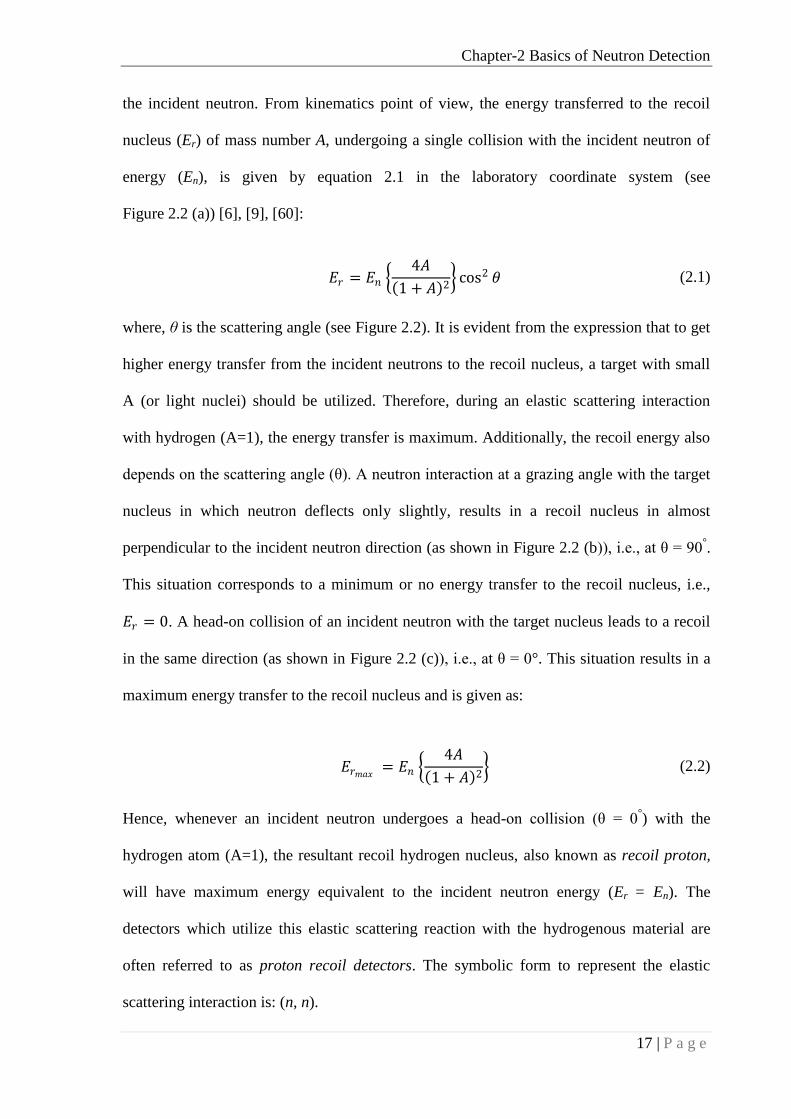
the incident neutron. From kinematics point of view, the energy transferred to the recoil
nucleus (Er) of mass number A, undergoing a single collision with the incident neutron of
energy (En), is given by equation 2.1 in the laboratory coordinate system (see
Figure 2.2 (a)) [6], [9], [60]:
𝐸𝑟 = 𝐸𝑛
4𝐴
1 + 𝐴 2 cos2 𝜃 (2.1)
where, θ is the scattering angle (see Figure 2.2). It is evident from the expression that to get
higher energy transfer from the incident neutrons to the recoil nucleus, a target with small
A (or light nuclei) should be utilized. Therefore, during an elastic scattering interaction
with hydrogen (A=1), the energy transfer is maximum. Additionally, the recoil energy also
depends on the scattering angle (θ). A neutron interaction at a grazing angle with the target
nucleus in which neutron deflects only slightly, results in a recoil nucleus in almost
perpendicular to the incident neutron direction (as shown in Figure 2.2 (b)), i.e., at θ = 90°.
This situation corresponds to a minimum or no energy transfer to the recoil nucleus, i.e.,
𝐸𝑟 = 0. A head-on collision of an incident neutron with the target nucleus leads to a recoil
in the same direction (as shown in Figure 2.2 (c)), i.e., at θ = 0°. This situation results in a
maximum energy transfer to the recoil nucleus and is given as:
𝐸𝑟𝑚𝑎𝑥= 𝐸𝑛
4𝐴
1 + 𝐴 2 (2.2)
Hence, whenever an incident neutron undergoes a head-on collision (θ = 0°) with the
hydrogen atom (A=1), the resultant recoil hydrogen nucleus, also known as recoil proton,
will have maximum energy equivalent to the incident neutron energy (Er = En). The
detectors which utilize this elastic scattering reaction with the hydrogenous material are
often referred to as proton recoil detectors. The symbolic form to represent the elastic
scattering interaction is: (n, n).
Page 52
2.2 Mechanisms of neutron interaction with matter
18 | P a g e
Figure 2.2 Neutron elastic scattering interaction diagram.
During inelastic scattering, part of the incident neutron kinetic energy is given to the
nucleus as excitation energy. After the collision, the excited nucleus immediately returns to
the ground state by ejecting one or more γ-rays. The total kinetic energy, in this case, is not
conserved. The total kinetic energy of the outgoing neutron and nucleus is less than the
kinetic energy of the incoming neutron because part of the original kinetic energy is used to
Incident
Neutron
(En)
Scattered
Neutron
Recoil Nucleus (Er)
Target Nucleus
θ
(a) Laboratory coordinate system
(b)
Incident
Neutron
(En) Target Nucleus
Recoil Nucleus (Er)
θ = 90°
Scattered
Neutron
Scattering at grazing angle [Energy transfer is Minimum, i.e., Er = ~ 0]
(c)
Recoil Nucleus (Er) θ = 0°
Target Nucleus
Scattered
Neutron
Incident
Neutron
(En)
Head-on scattering [Energy transfer is Maximum, i.e., Er = ~ En]
Page 53
Chapter-2 Basics of Neutron Detection
19 | P a g e
place the nucleus into the excited state. A point worth to note here is that the inelastic
scattering is not possible if all the excited state of the nucleus are at higher energy levels
than the incident neutron energy. Since the hydrogen nucleus does not have an excited
state, it would always undergo elastic scattering reaction. Symbolically, the inelastic
scattering reactions can be represented as: (n, n').
2.2.2 Absorption interaction
In the absorption reaction, the incident neutron is captured or absorbed in the target
nucleus and one or more particles are emitted. Absorption reactions can be further
subdivided into two main categories: radiative capture and non-radiative capture.
In radiative capture (n, γ), the target nucleus captures the incident neutron and
moves into an excited state. The excited nucleus decays abruptly emitting single or cascade
of γ–rays.
In non-radiative capture, the target nucleus captures the incident neutron and emits
one or more neutrons (n, 2n), (n, 3n); charged particles such as protons (n, p), alpha (n, α),
deuterons (n, d), tritons (n, t), etc. Majority of these interactions are endothermic, hence
neutrons above specific threshold energies can only trigger them. However, there are few
isotopes such as 3He,
6Li,
10B, and
157Gd that can endure exothermic interactions. Materials
based on the aforementioned isotopes have the potential to be used as neutron detectors.
Fission (n, f) is another type of neutron interaction, which occurs when the neutron
interacts with a heavy nucleus (Z ≥ 92). As a result of the fission due to neutron capture,
fissioning compound nucleus splits into two smaller nuclei (known as fission fragments),
along with the release of two or more free neutrons, few γ–rays, and neutrinos.
A summary of several interaction types is tabulated in Table 2.1.
Page 54
2.2 Mechanisms of neutron interaction with matter
20 | P a g e
Table 2.1 Types of neutron interactions.
Type (Nomenclature) Nuclear Reaction
Elastic Scattering (n, n) X + 𝑛 → X + 𝑛𝑍𝐴
𝑍𝐴
Inelastic Scattering (n, n') X + 𝑛 → X + 𝑛𝑍𝐴
𝑍𝐴 + γ
Radiative Capture (n, γ) X + 𝑛 → X𝑍𝐴+1
𝑍𝐴 + γ
Charged Particle Emission (n, α) X + 𝑛 → X𝑍−1𝐴−3
𝑍𝐴 + α
Charged Particle Emission (n, p) X + 𝑛 → Y𝑍−1𝐴
𝑍𝐴 + p
Neutral Particle Emission (n, 2n) X + 𝑛 → X𝑍𝐴−1
𝑍𝐴 + 2n
Fission (n, f) X + 𝑛 → 𝑌 + 𝑍 + γ + 𝑛𝑍𝐴
2.2.3 Neutron interaction cross-section
All the possible interactions of a neutron with the matter, discussed in the previous
section, have a certain probability of occurrence which is generally explained through the
concept of cross-section. The probability of a particular interaction (i) between a neutron
and a single nucleus is expressed by the microscopic cross-section (𝜍𝑖). It depends on the
target material (isotopes), type of interaction, incident particle and its energy. Its unit is
barn (b) (1 b equals to 10-24
cm2). An incident neutron may experience a variety of
interactions while moving in a medium. Total cross-section is the sum of all the individual
cross-sections:
𝜍𝑡𝑜𝑡𝑎𝑙 = 𝜍𝑒𝑙𝑎𝑠𝑡𝑖𝑐 + 𝜍𝑛 ,𝛾 + 𝜍𝑛 , 𝑛 ′ + 𝜍𝑛 ,2𝑛 + 𝜍𝑛 ,𝛼 + ⋯⋯⋯ (2.3)
The microscopic cross-section describes the neutron interaction with a single nucleus.
However, in general, a neutron beam interacts with a thick sample which may contain
several elements. Such scenarios can be explained by the macroscopic cross-section
(Σ) (cm-1
), and it is expressed by equation (2.4):
Σ = 𝑁𝑖 . 𝜍𝑖 (2.4)
where Ni is the atom density given as:
𝑁𝑖 = 𝜌
𝑁𝐴 . 𝑛𝑖
𝑀 (2.5)
Page 55
Chapter-2 Basics of Neutron Detection
21 | P a g e
where, ρ is the density of the material (kg/m3), NA is the Avogadro constant (NA = 6.022 ×
1023
atoms/mol), and M is the molar mass of the material (kg/mol).
Another important concept is the mean-free-path (λ = 1/Σ), which represents the
average distance traveled by neutron between two successive interactions. The λ depends
on the type of material and energy of the incident neutron. After each interaction, the
energy decreases, thereby changing the value of λ.
The relationship between energy (E) and velocity (v) of the neutron is expressed as:
𝑣 = 1.383 × 10⁷. 𝐸1 2 (2.6)
Fast neutrons of energy 1 MeV travel with a velocity of 1.383 × 10⁷
m/s whereas thermal
neutrons (energy = 25 meV) traverse with a velocity of 2187 m/s. Therefore, thermal
neutrons (slow neutrons) tend to spend more considerable time in the medium than the fast
(high energy) neutrons. That is the reason why slow neutrons have a higher probability of
interaction with the material in comparison to the fast neutrons. Figure 2.3 shows the
typical neutron total cross-section plot for the 3He,
10B, and
6Li isotopes. It can be observed
that the cross-section generally decreases with neutron energy. As can be seen, the cross-
section for the fast neutron is relatively quite low. Thus, the detection of fast neutrons is
quite challenging in comparison to slow neutrons. Considering the neutron cross-sections,
the detection of neutrons is subdivided into two groups viz., (a) slow neutron detection (b)
fast neutron detection.
Slow or Thermal (En = 25 meV) Neutron detection
Slow neutrons have very small K.E., therefore they transfer very little energy to the
target nucleus through elastic scattering reaction. The recoil nucleus will have very low
energy to create significant ionization. Moreover, slow neutrons have comparatively higher
cross-section for absorption reaction, which results in a secondary charged particle
Page 56
2.2 Mechanisms of neutron interaction with matter
22 | P a g e
generation. The K.E. of these charged particles depends on the reaction Q-value. These
charged particles lose their K.E. through ionization mechanisms which in turn generate
electron-hole or electron-ion pairs in the detector sensitive region. Now, these charge pairs
are collected to form the detector signal. Table 2.2 lists out a few of the slow neutron
converter materials of interest along with the secondary particles generated as a result of
neutron interaction and their cross-sections. Note that these converter materials can be
coupled with all the detector types such as gas-filled, scintillators or solid-state detectors
(briefly explained in section 2.3) [9].
Table 2.2 Converter materials for thermal neutron detection.
Thermal neutron reactions Reaction Q-value
(MeV)
Cross-section
(barn)
n + 3He →
3H + p 0.765 5330
n + 10
B → 7Li + α (6.3%)
n + 10
B → 7Li + α (93.7%)
2.79 3840
n + 6Li →
3H + α 4.78 940
n + 155
Gd → 156
Gd + γ + e- 0.59 60791
n + 157
Gd → 158
Gd + γ + e- 0.54 255011
Figure 2.3 Total neutron cross–sections for 3He,
6Li, and
10B isotopes [62].
Page 57
Chapter-2 Basics of Neutron Detection
23 | P a g e
Fast Neutron detection
Fast neutrons can be detected mainly by two methods viz., neutron moderation or
elastic scattering interaction. In the first method, fast neutrons are moderated or slowed
down to thermal energy region via elastic and inelastic scatterings with suitable moderator
material; the resultant slow neutrons can then be detected by any slow neutron detection
method. The second method relies on the relatively high cross-section of fast neutrons for
elastic scattering reaction with hydrogenous (hydrogen-rich) materials. The fast neutrons
generate recoil nucleus which is detected by any charged particle detector. For example,
hydrogenous material HDPE generates recoil protons after elastic scattering reactions with
fast neutrons. This method is popularly known as the recoil proton method.
2.2.4 Charged particle interaction with matter
Since, the detection of neutrons is indirectly recorded by the energy deposited by the
charged particles in the detector active region. Hence, it is imperative to understand the
mechanisms by which charged particle interacts and loses energy as it moves through
matter. A charged particle traversing through matter can initiate processes such as:
Coulomb interactions (ionization & excitation of atoms), emission of electromagnetic
radiation (bremsstrahlung), emission of Cerenkov radiation and nuclear interactions. The
ionization occurs, when the charged particle have enough energy to remove an electron.
This results in a creation of ion pairs in surrounding matter. The excitation takes place
when the electron acquires enough energy to move to an empty state in another orbit of
higher energy. All these processes cause energy loss of the traversing particles. The relative
contribution of these various processes to the total energy loss depends on the kinetic
energy of the particle, the detector material, etc. For detailed understanding refs. [9], [61]
may be referred.
Page 58
2.3 Types of neutron detectors
24 | P a g e
2.3 TYPES OF NEUTRON DETECTORS
This section briefly explains three main categories of traditional radiation detectors.
2.3.1 Gas-filled detectors
As the name suggests, these detectors are filled with noble gas which is ionized by
the charged particles going through it. The gas-filled detectors consist of two electrodes
(Figure 2.4) to which a specific voltage is applied. The ionizing radiation ionizes the gas
atoms and creates electron-ion pairs which drift under the influence of the applied electric
field. Their motion towards electrodes induces the electrical current in associated
electronics which is further processed for counting purpose. Depending upon the region of
operation, gas-filled detectors are divided in three types viz., ionization chamber,
proportional counters, and gieger-müller (GM) counters. The ionization chambers are
operated at low electric field such that no gas multiplication takes place. The current is
independent of applied voltage. They are preferred for high radiation dose rates due to no
dead-time. Proportional counters are operated at slightly higher voltage so that each ion pair
produces an avalanche current. The output current pulse is proportional to the energy
deposited by the radiation. GM counters are operated at even higher voltages so that each
ion-pair create multiple avalanches which spread along the anode wire. GM tubes produce
large output signal with minimal electronic processing.
In order to detect neutrons, a layer of neutron sensitive converter material (described
in the previous section) is coated on the inner wall of the cylindrical chamber. The incident
neutron interacts with the coated material and generates secondary charged particles. These
charged particles now create ionization (electron-ion pairs) in the filled gas which is
collected to indicate the presence of neutrons. These detectors are mostly used for neutron
detection in nuclear applications because they are highly resistant to radiation-induced
Page 59
Chapter-2 Basics of Neutron Detection
25 | P a g e
damages, and offer high efficiency to thermal neutron detectors with good gamma-
background discrimination [9]. Some major drawbacks include large dimension and
requirement of the high voltage supply (order of hundreds of volts), and high pressure (≈ 10
bar) for its operation. The purity of filled-gas, wall-effects, and space-charge effects are
other major concerns for the gas-filled detectors [9].
2.3.2 Scintillation detectors
Scintillators are materials which generate scintillation of photons in the visible light
range when the ionizing radiation passes through them. These materials can be of solid,
liquid or gaseous type. The light emitted from the scintillator is minimal. Therefore, it is
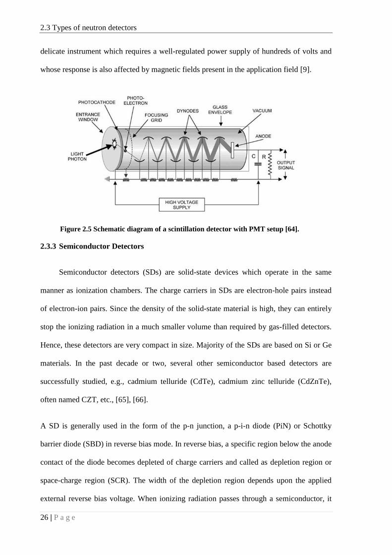
amplified with the help of a photomultiplier tube (PMT) as shown in Figure 2.5. Thermal
neutrons can be detected by means of a nuclear reaction with 6Li nuclei by using
6Li-
containing scintillation materials (loaded scintillators) such as 6LiI(Eu) [9]. Fast neutrons
can be detected by any organic (plastic or liquid) scintillators by means of elastic scattering
[63]. The scintillation detectors have a wide range of applications. They offer a fast
response (1‒5 µs) than gas-filled detectors. However, scintillator detectors need PMT, a
Figure 2.4 Schematic diagram of a typical Gas-filled detector.
Detector
Electronics
Voltage
Source
Anode
Cathode
Filled-Gas
+ + + + +
- - - - -
Incident
Radiation
Page 60
2.3 Types of neutron detectors
26 | P a g e
delicate instrument which requires a well-regulated power supply of hundreds of volts and
whose response is also affected by magnetic fields present in the application field [9].
Figure 2.5 Schematic diagram of a scintillation detector with PMT setup [64].
2.3.3 Semiconductor Detectors
Semiconductor detectors (SDs) are solid-state devices which operate in the same
manner as ionization chambers. The charge carriers in SDs are electron-hole pairs instead
of electron-ion pairs. Since the density of the solid-state material is high, they can entirely
stop the ionizing radiation in a much smaller volume than required by gas-filled detectors.
Hence, these detectors are very compact in size. Majority of the SDs are based on Si or Ge
materials. In the past decade or two, several other semiconductor based detectors are
successfully studied, e.g., cadmium telluride (CdTe), cadmium zinc telluride (CdZnTe),
often named CZT, etc., [65], [66].
A SD is generally used in the form of the p-n junction, a p-i-n diode (PiN) or Schottky
barrier diode (SBD) in reverse bias mode. In reverse bias, a specific region below the anode
contact of the diode becomes depleted of charge carriers and called as depletion region or
space-charge region (SCR). The width of the depletion region depends upon the applied
external reverse bias voltage. When ionizing radiation passes through a semiconductor, it
Page 61
Chapter-2 Basics of Neutron Detection
27 | P a g e
ionizes the matter, thereby creating free electron-hole pairs (EHPs). The total number of
EHPs created is proportional to the energy transmitted by the radiation to the
semiconductor. These EHPs drift towards the respective electrodes and induce image
charges on the electrodes which are amplified and processed by associated detector
electronics to provide the detector response [67]. The operation of a typical semiconductor
detector is illustrated in Figure 2.6 and a typical schematic of the detector electronics is
shown in Figure 2.7. The SDs are basically a very high resolution charged particle and
photon detectors. In the recent past, several semiconductor based neutron detector
prototypes have been developed. The semiconductor-based neutron detectors can be
classified into two groups:
Figure 2.7 Schematic of detector electronics.
Semiconductor sensor generates a small electrical signal after capturing the incident radiation. This
low-level electrical signal is amplified in pre-amplifier; shaped in pulse shaper and then digitized for
storage and further analysis [67].
Semiconductor
Figure 2.6 Schematic of a semiconductor diode detector.
Detector
Electronic
s
Anode
Cathode
Voltage
Supply
Incident
Radiation
Page 62
2.3 Types of neutron detectors
28 | P a g e
Direct-conversion or bulk neutron detectors
These are the detectors whose bulk semiconducting material is itself sensitive to the
neutrons, e.g., GaAs, CZT, Diamond, UO2, BxC, etc., [66]. A typical schematic of a direct
conversion neutron detector is shown in Figure 2.8 (a). Neutron directly interacts with the
nucleus of the bulk material and generates recoil nucleus or secondary charged particles,
which further lose their energy in the detector active (depletion) region to generate the
detector signal. This kind of detectors could be highly efficient. However, semiconductors
having a large amount of neutron sensitive isotopes, are rare and they suffer from poor
charge collection properties [68].
Figure 2.8 Representation of (a) Direct (b) Indirect-Conversion Neutron Detectors.
Indirect−conversion neutron detectors
The indirect conversion semiconductor detectors (as shown in Figure 2.8 (b)) have an
additional coating of a neutron sensitive converter material. The incident neutrons interact
with the coated neutron sensitive converter and generate secondary charged particles which
in turn create e-hole pairs in the semiconductor depletion region to provide the detector
signal. A planar and few 3D structures of indirect configuration neutron detector are shown
in Figure 2.9 [68]. A point to note here is that the planar structure of SDs is matured while
Page 63
Chapter-2 Basics of Neutron Detection
29 | P a g e
several 3D structures are still under theoretical investigation as they pose a severe challenge
in terms of fabrication and efficient charge collection.
Figure 2.9 Schematic of the (a) planar structure of SD; few 3D structures (b) Stacked SD (c)
single side trench structure (d) double side trench structure [68].
The planar and stacked structure of the indirect-conversion SiC-based semiconductor
neutron detector has been studied in this work. The planar structure has an inevitable
geometrical limitation because the probability of neutron interaction in a planar structure
depends strongly on the thickness of the neutron sensitive converter layer. The probability
of the neutron interaction increases with the thickness of the converter layer, but at the
same time, it reduces the probability of resultant secondary charged particles to reach the
active (depletion) region of the SD (due to continuous energy loss in the matter, also known
as self-absorption). A careful observation reveals that, in planar structure, not all the
secondary charged particles are able to reach the depletion region of the SD as some of the
low energy are absorbed within converter and few others are leaving the converter from
sides, i.e., unable to reach depletion region of the semiconductor (depicted in Figure 2.10).
(a)
Converter
Semiconductor
(b)
Converter
Semiconductor
(c) (d)
Page 64
2.3 Types of neutron detectors
30 | P a g e
Therefore, for each converter material, there is an optimum thickness at which maximum
number of reaction products would reach in the SD's depletion region. The optimum
thickness of the converter is not feasible to determine through experiments. Hence, Monte-
Carlo simulations have been performed to find the optimum thickness for several neutron
sensitive converter materials.
Figure 2.10 Sketch of planar SD illustrating various possibilities of secondary charged
particles movement which reflects whether the neutron is detected or undetected.
Note: Dashed lines indicate the track of charged particles or recoil proton whereas continuous
line represents neutron tracks.
After understanding the role of converter material, it is prudent to specify the
important characteristics of a neutron sensitive converter material:
The converter should be made up of isotopes or compound material having a high
percentage of those isotopes that captures neutrons.
It should have a high neutron cross-section for the energy range of interest.
Converter which emits charged particles such as (n, α), (n, p) should be preferred
over those which emit uncharged particles like (n, 2n), (n, γ) because it is easier to
detect charged particles.
The energy of generated charged particles should be sufficiently high to cross the
converter and deposit sufficient energy in the detector active region.
Page 65
Chapter-2 Basics of Neutron Detection
31 | P a g e
2.4 METAL-SEMICONDUCTOR (M-S) JUNCTION
A M-S junction can be rectifying (Schottky contact) or non-rectifying (ohmic
contact). In this work, SiC has been used in the form of a SBD. Therefore, it is essential to
understand the Schottky contact formation and current transport mechanism through it. It
should be noted that, the theory is briefly described considering n-type SiC SBD. For
detailed understanding, semiconductor textbooks should be referred [69]–[72].
2.4.1 Schottky contacts
Schottky contacts allow conduction of current in one direction but blocks it in the
other direction. Figure 2.11 (a) shows the energy band diagrams of metal and SiC
semiconductor material before making any contact. When the metal is brought into contact
with the semiconductor, electrons in the high energy states of the semiconductor flow into
the lower energy states of the metal until the Fermi level becomes a constant throughout the
system, i.e., until the thermal equilibrium (zero bias) condition is achieved. Also, the metal
work-function (Φ𝑀) should be different than the semiconductor work-function (Φ𝑆) (for n-
type semiconductor Φ𝑀 > Φ𝑆 and vacuum level must be continuous across the interface.
The above requirements results in a unique energy band diagram (as shown in
Figure 2.11 (b)) for an ideal M-S contact where interface states* are absent. The electrons
that flow into the metal leave behind the positively charged donor atoms in the
semiconductor, creating a space charge region or depletion region. The excess electrons in
the metal side and positive ionized donors in semiconductor create electric field from
semiconductor to metal. The alignment of the Fermi level results in a Schottky barrier
height (𝜙𝐵) on the metal side and a built-in potential (Vbi) on the semiconductor side.
Schottky barrier height (SBH) is the barrier seen by electrons in the metal trying to move
* Interface states are present between the metal-semiconductor boundaries. They arise from many kinds of
defects such as broken/dangling bonds at the semiconductor surface.
Page 66
2.4 Metal-Semiconductor (M-S) Junction
32 | P a g e
into the semiconductor, and is ideally given by:
𝜙𝐵 = Φ𝑀 − 𝜒𝑆 (2.7)
where, 𝜒𝑆 is the energy difference between the conduction band edge Ec and the
vacuum level known as electron affinity of the semiconductor. Ideally, the SBH
depends on the metal and semiconductor properties as evident from equation (2.7).
However, in case of practical M-S contact, the SBH is independent of the metal due to
the interface states present between the M-S boundaries. These states are continuously
distributed in energy within the forbidden gap (Eg), as shown in Figure 2.11 (c).
Figure 2.11 Energy band diagram of metal n-type semiconductor contact with ΦM > ΦS.
(a) When two materials are isolated from each other (b) thermal equilibrium condition after the
contact is made. (c) Fermi level pinning due to interface states.
These states pinned down the Fermi level (Ef) at the surface, and thus the SBH will be
independent of metal work function and is given by:
𝜙𝐵 = 𝐸𝑔 − 𝐸𝑓 (2.8)
Page 67
Chapter-2 Basics of Neutron Detection
33 | P a g e
Most of the M-S contacts do have the interface states, but they are not large enough to be
pinned down to the Fermi level. Thus, the SBD will be affected by both the metal work
function as well as the interface states. Most of the metals deposited on the SiC, work as
Schottky contact provided SiC is not heavily doped and high-temperature (>700 °C)
contact sintering is not performed [29]. In SiC, the SBH is found to be dependent on the
SiC polytype, the metal, the surface condition before contact formation and the interfacial
chemistry. The work-function of some metals used for Schottky contact on SiC is tabulated
in Table 2.3.
Table 2.3 Work-function of several metals for Schottky contact formation on SiC [73].
Metal Mg Mn In Ag Al Ti Mo Cu Au Pd Ni Pt
𝚽𝑴 (eV) 3.65 4.15 4.20 4.25 4.28 4.33 4.6 4.65 5.1 5.12 5.15 5.65
Apart from the presence of interface states, SBH can also be modified by the
Coulomb attraction between the electron and its image charge in the metal, known as an
image force lowering. The magnitude of the image force lowering (∆𝜙𝑏𝑙 ) is expressed as
[70], [71]:
𝜙𝑏𝑙 = 𝑞𝐸
4𝜋휀𝑠 (2.9)
where E is electric field, q is electron charge and 휀𝑠 is image force permittivity.
2.4.2 Ohmic Contacts
Ohmic contact is a non-rectifying contact which allows free-flow of charge carriers in
both the directions. Ohmic contacts are also significant from the semiconductor device
operation point of view. Ohmic contacts have negligible contact resistance compared to
total device resistance [70]. For M-S contact to achieve very low contact resistance, it must
have either a small barrier height or very high doping density (with an increase in doping,
Page 68
2.4 Metal-Semiconductor (M-S) Junction
34 | P a g e
contact resistance decreases exponentially) or both [70]. It is difficult to produce a small
barrier height as it depends on several factors as explained in the previous section.
Therefore, Ohmic contacts are fabricated using highly doped semiconductors to achieve
this low contact resistance.
2.4.3 Current transport mechanism
In M-S junctions, majority carriers are predominantly responsible for the current
transport, unlike p-n junctions, where minority carriers are also accountable for the flow of
current. The majority carriers can either be electrons (for n-type semiconductors) or holes
(for p-type semiconductors) [70]. Four mechanisms contribute to the current transport
across M-S interface [26], [70], [71]:
i. Thermionic Emission (TE): The emission of electrons over the Schottky barrier from
the semiconductor into the metal. TE is dominant for lightly doped semiconductors.
ii. Quantum mechanical tunneling: It is dominant for highly doped semiconductors
such that the barrier is sufficiently thin. Tunneling can be ‗pure‘ tunneling, i.e., field
emission (FE) at low temperatures when electrons' energies are close to the Fermi
level or thermionic field emission (TFE) at high temperatures when electrons are
excited to levels where barrier is sufficiently thin for tunneling to occur [70], [72].
iii. Carrier recombination and generation in the depletion region, and
iv. Hole injection from the metal to the semiconductor (recombination in the neutral
region).
These transport mechanisms are illustrated in Figure 2.12. In the case of wide
bandgap semiconductors such as SiC, the thermionic emission and tunneling of electrons
over the Schottky barrier contribute dominantly to the current density. If the SiC material is
lightly doped and the operating temperature is not very low, the thermionic emission (TE)
Page 69
Chapter-2 Basics of Neutron Detection
35 | P a g e
current will be dominant. The tunneling component will only be significant if the SiC is
heavily doped and the device is operating in a low-temperature environment. Under reverse
bias operation, the tunneling current term contributes significantly.
Figure 2.12 Basic current transport mechanisms across the M-S junction.
(1) Thermionic emission, (2) Tunneling, (3) Recombination, (4) Diffusion of holes, [26], [27],
[70], [71].
2.4.4 Current-Voltage (I-V) relationship
The current conduction in the Schottky diode is mainly due to the majority carriers
and can be explained by the thermionic emission (TE) theory [70]. The current density of
the Schottky diode at forward and reverse bias can be expressed by the relation:
𝐽 = 𝐽𝑠 𝑒𝑥𝑝
𝑞𝑉
𝜂𝑘𝑇 − 1 (2.10)
where q is electron charge, V is forward bias voltage, η is ideality factor, k is Boltzmann
constant, T is temperature (in Kelvin), and Js is the reverse saturation current density
derived from the straight line fitting of the equation (2.10) at zero biasing and given by
equation (2.11):
𝐽𝑠 = 𝐴∗ 𝑇2 𝑒𝑥𝑝
−𝑞 𝜙𝐵 − Δ𝜙𝑏𝑙
𝑘𝑇 (2.11)
Page 70
2.4 Metal-Semiconductor (M-S) Junction
36 | P a g e
where 𝜙𝐵, Δ𝜙𝑏𝑙 , and A* is the barrier-height (BH), image-force lowering and Richardson
constant, respectively. The value of A* for 4H-SiC is 146 A-cm
-2-K
-2 [74]. The ideality
factor (η) explains the deviation of I-V characteristics from the TE theory and can be
expressed by rearranging the equation (2.10) as:
𝜂 =
𝑞
𝑘𝑇
𝑑𝑉
𝑑 ln 𝐽 (2.12)
For the ideal diode, the value of η is 1, but for the practical diodes, its value is greater
than 1. The semi-log plot of J-V curve (i.e., ln(J) vs. V plot) at lower forward bias gives a
straight line. The slope of this linear region {d(ln (J))/dV} is used to predict the ideality
factor of the diode. The intercept of this linear region with the Y-axis provides value of
ln(JS). The Schottky barrier-height (𝜙𝐵) can be estimated from the equation (2.13) using the
value of Js obtained from the intercept of ln(J)-V plot.
𝜙𝐵 =
𝑘𝑇
𝑞 ln
𝐴∗ 𝑇2
𝐽𝑠 (2.13)
It should be noted that the value of 𝜙𝐵 estimated from the J-V curve is only reliable if the
forward bias plot of ln(J) vs. V is linear with a low value of η. To determine the series
resistance (RS), the model given by Cheung and Cheung [75] is used. The slope of the
dV/d(ln(I)) vs. I curve gives the RS.
2.4.5 Capacitance-Voltage (C–V) relationship
Few critical device parameters such as built-in-potential (Vbi), effective carrier
density (Neff), Fermi energy (Ef), image-force lowering (Δ𝜙𝑏𝑙 ) are estimated from the C-V-
characteristics. In reverse bias SBD, the depletion or space charge region (SCR) formed at
Schottky metal and semiconductor interface acts as a voltage dependent capacitor
(C=dQ/dV). The reverse bias junction capacitance can be expressed as [70]:
Page 71
Chapter-2 Basics of Neutron Detection
37 | P a g e
𝐶 = 𝐴 𝑞휀𝑠휀0𝑁𝑑
2 𝑉𝑏𝑖 + 𝑉𝑅 (2.14)
where A, 휀𝑠 , 휀0, Nd, and VR is the area of Schottky contact, dielectric constant, the
permittivity of vacuum (휀0= 8.85 × 10⁻¹⁴
F/cm), doping concentration, and reverse bias
voltage, respectively. Equation (2.14) can be rewritten as:
1
𝐶2=
2 𝑉𝑏𝑖 + 𝑉𝑅
𝑞휀𝑠휀0𝑁𝑑 (2.15)
It shows that the inverse squared capacitance is the linear function of the applied reverse
bias voltage [70]. The intercept at the voltage axis of the {(1/C2) vs. V} plot provides the
value of Vbi, whereas the slope of the linear curve is used to determine the doping
concentration (Nd) of the diode epitaxial layer using equation (2.16):
𝑁𝑑 =
2
𝑞휀𝑠휀0
1
𝑠𝑙𝑜𝑝𝑒 (2.16)
Using the values of 𝑉𝑏𝑖 and 𝑁𝑑 , the barrier height (𝜙𝐵𝐶−𝑉), Ef, Δ𝜙𝑏𝑙 , effective carrier
density (Nc) and depletion width (Wd) can be estimated by the following relations:
𝜙𝐵𝐶−𝑉= 𝑉𝑏𝑖 + 𝐸𝑓 − Δ𝜙𝑏𝑙 (2.17)
𝐸𝑓 =
𝑘𝑇
𝑞ln
𝑁𝑐
𝑁𝑑 (2.18)
𝑁𝑐 = 4.82 × 10¹⁵ 𝑇3/2 𝑚𝑒∗ 𝑚0 3/2 (2.19)
where 𝑚𝑒∗ is the effective mass of electron and 𝑚0 is the rest mass of electron (𝑚𝑒
∗=
0.42𝑚0).
Δ𝜙𝑏𝑙 = 𝑞𝐸
4𝜋휀𝑠
(2.20)
𝑊𝑑 = 2휀𝑉𝑏𝑖
𝑞𝑁𝑑 (2.21)
Page 72
2.5 Defects in semiconductors
38 | P a g e
2.5 DEFECTS IN SEMICONDUCTORS
Defects in semiconductors can be defined as any form of imperfection or deviation
from a perfect crystal lattice. As a matter of fact, a perfect semiconductor crystal is
impossible to produce due to several reasons that include wafer production, growth
methods, and device processing. Defects are also introduced intentionally as a donor
impurity into the semiconductor to modify the conductivity of the semiconductor device.
Defects can be categorized as intrinsic and extrinsic defects. A defect is of intrinsic type if
the defective volume is composed of the same atoms as the undisturbed crystal lattice. If
foreign atoms, such as doping impurities, take part in the defect, the defect is said to be of
extrinsic character. Intrinsic defects are point defects (0-dimension), line defects (1-D),
plane defects (2-D) and volume defects (3-D). The subsequent subsections are focused on
the defects in SiC. For detailed description refs. [26], [27], [72], [76] can be followed.
2.5.1 Primary Defects
Primary defects can be classified into two categories, namely, point defects and
extended defects. Point defects are not extended in space in any dimension, and this implies
that the perturbation of the lattice is localized about a lattice site and involves only a few
nearest neighbors. On the other hand, extended defects are extended in nature (such as grain
boundaries, dislocations or stacking faults) [76].
Point defects can be further sub-divided as:
i. Vacancy: An atom is missing from its original lattice position. The vacancy in SiC
can either be silicon vacancy, VSi (there is no atom on a silicon lattice site) or carbon
vacancy, VC (there is no atom on a carbon lattice site).
Page 73
Chapter-2 Basics of Neutron Detection
39 | P a g e
ii. Interstitial: An atom that inhabits a position different from its regular site.
Interstitials can be classified as self-interstitials (i.e., if the atom is the same as one of
the species of the host lattice), or an interstitial impurity (i.e., if the interstitial atom is
a different species from the host atoms). In SiC, a self- interstitial can either be
silicon, Sii or carbon, Ci.
iii. Frenkel pair: A self-interstitial atom is located close to a vacancy.
iv. Antisite: In compound semiconductors, an atom of one sub-lattice is positioned in a
lattice site of the other element, e.g., in SiC, when Si takes the lattice position of C (a
silicon antisite, SiC) or C is on a Si lattice point (a carbon antisite, CSi).
v. Substitutional impurity: A foreign atom that occupies a lattice site, e.g., a nitrogen
atom on a C site (NC).
Point defects are shown schematically in Figure 2.13.
Figure 2.13 The schematic diagram of point defects in semiconductors, taken from [76].
2.5.2 Secondary defects
Due to high-energy particle irradiation, primary defects such as vacancy (V) and self-
interstitial (I) are created in semiconductors. The primary defects are mobile at low
Page 74
2.5 Defects in semiconductors
40 | P a g e
temperatures. The V and I which survive the recombination can diffuse into the
semiconductor and interact with other intrinsic and extrinsic defects which results in
another complex room temperature stable defects such as A-center, E-center, divacancy,
etc. The removal of two neighboring atoms forms the divacancy (V-V). The E-center can be
described as a vacancy trapped next to a substitutional donor atom. The A-center (V-O)
may be regarded as a vacancy trapped next to an oxygen atom in an interstitial position.
Most of the primary and secondary defects discussed above are electrically active
and introduce electronic states in the band gap of semiconductors, which can be classified
as shallow levels and deep-levels [29], [76]. Shallow levels are those defects whose states
are located near the band edges (near valence band for acceptor type levels and near
conduction band for donor type levels). Deep levels are those defects which are positioned
deeper in the band gap [26]. Deep-levels can be described as an electron trap, a hole trap, a
recombination center or a generation center, depending on the nature of the electron and
hole interactions that happens between the deep-levels and the conduction and valence
bands. Figure 2.14 illustrates the possible interactions that can take place between the bands
and the deep levels through the emission and/or capture of charge carriers. The possible
interactions are:
a) a deep level can capture an electron from the conduction band with capture rate cn
after which any of two interactions (b) or (c) may occur,
b) the deep level can either emit the electron back to conduction band with emission rate
en, or
c) it can capture a hole from the valence band with capture rate cp
d) After hole capture, again two interactions are possible: either the hole can be emitted
to the valence band with emission rate ep, or an electron can be captured from the
conduction band (i.e., process (a) follows).
Page 75
Chapter-2 Basics of Neutron Detection
41 | P a g e
Figure 2.14 The schematic diagram of different carrier transitions between deep-levels and
the energy bands.
(a) Electron capture, (b) electron emission, (c) hole capture, and (d) hole emission [72]. The
subscript ‗T‘ stands for traps. Trap centers occupied by electrons are nT and occupied by holes are
pT. The total density NT = nT + pT.
An electron trap is a deep level for which the cn is much higher than the cp and vice-
versa for a hole trap (cp>>cn). If cn ≈ cp then the deep level is recombination center. From
Figure 2.14, a recombination event is the combination of processes (a) and (c), and a
generation event is (b) and (d). A defect where these processes occur is called a generation-
recombination center.
Deep levels can either be beneficial or detrimental to device operations, depending on
their applications. Thus, the study of deep levels is of paramount importance in the
semiconductor device industry so that those deep levels which are useful can be
deliberately added and those that are detrimental can be reduced or eliminated.
The deep-levels and their associated properties (signatures) are studied using several
techniques such as Deep Level Transient Spectroscopy (DLTS), Thermally Stimulated
Current (TSC), Thermally Stimulated Capacitance (TSCAP), Photo-induced Transient
Spectroscopy (PITS), etc., whose descriptions are beyond the scope of this thesis.
Page 76
2.5 Defects in semiconductors
42 | P a g e
2.5.3 Defects in SiC
This subsection gives a brief account of defects that are reported to be found in 4H-
SiC. Epitaxial layers grown on off-axis {0001} SiC substrates exhibit several types of
surface defects such as carrot defect, triangular defect, and downfall [29]. When SiC
devices include carrot or triangular defects, the devices exhibit excessive leakage currents
and significantly decreased breakdown voltages [77]. Another type of defect is Micropipes.
Micropipes are basically a hollow core penetrating the entire wafer along the c-axis*
direction. Placing any device directly on top of the micropipe is bound to cause failure.
Micropipes may be caused by several screw dislocations† bunching together to form a giant
screw dislocation, making it energetically favorable to open up a hollow core in the center.
Nevertheless, substrates are commercially available with zero or ~ 1 micropipe density/cm2
[78], [79]. Stacking faults (SFs) are another kind of defects that exist in SiC. SFs occur due
to the deviation of Si–C bilayers from the perfect stacking sequence along the c-axis of the
crystal. SFs reduce the barrier height and the breakdown voltage of a Schottky diode [80].
Deep-levels are observed in as-grown and irradiated n-type 4H-SiC. They exist at
specific energy levels (Et) within the band gap region. They capture the created charge
carriers (electrons or holes) and immobilize them for a period of time or even neutralize
them completely. The trap energy level (Et) for specific carrier traps is referred as relative
to the band energy. So, for electron trapping, Et is given with reference to the conduction
energy band as: (Ec−Et) and for hole trapping, Et is given with respect to the valance band
as: (Ev+Et). Two dominant deep-levels are widely reported in 4H-SiC: the Z1/2 [81] (EC −
0.68 eV) and the EH6/7 [82] (EC − 1.65 eV) with densities ~ 1013
cm-3
. Both defects are
extremely stable against high-temperature (~ 1700 °C) annealing. They are related to the
*For hexagonal structures, four principal axes are commonly used a1, a2, a3 and c. The three a-vectors (with
120° angle between each other) are all in the close-packed plane called a-plane, whereas the c-axis (0001) is
perpendicular to this plane. † Screw dislocations formed when atoms are arranged in a helical pattern normal to the direction of stress.
Page 77
Chapter-2 Basics of Neutron Detection
43 | P a g e
Carbon vacancy [83]. In the lower half of the band-gap, the HK2 (EV + 0.84 eV), HK3 (EV
+ 1.24 eV) and HK4 (EV + 1.44 eV) [84] centers are dominant deep levels. The densities of
HK2, HK3 and HK4 centers are typically in the range (1–4) ×1012
cm−3
. The origins of
these defects are related to the defect complexes including carbon displacement. Since, the
HK2, HK3, and HK4 centers almost disappear upon annealing at 1450–1550 °C [84], the
Z1∕2 and EH6/7 centers are more important. Indeed, the Z1∕2 center has been identified as the
dominant lifetime killer, at least for n-type 4H-SiC [85]. After irradiation of 4H-SiC with
electrons, some new deep-levels are observed in addition to the increase in the
concentration of the existing deep-levels (Z1∕2 and EH6/7). These deep-level centers are
referred to as EH1 (EC – 0.45 eV), EH2 (EC – 0.68 eV), EH4 (EC – 0.72 eV), EH5(EC –
1.15 eV), EH6/EH7 (EC – 1.65 eV) and HH1 (EV +0.35 eV) [82], [86]. Following the
neutron irradiation, deep-levels (EC – 0.5 eV, EC – 0.24 eV, and EC – 0.13 eV) were
observed in 4H-SiC [29], [56]. The list is too exhausting to present here. For extensive
details a review of deep levels in SiC by Lebedev et al., [87] may be referred.
2.5.4 Effects of irradiation induced defects
Irradiation-induced defects in the semiconductors may alter the lifetime of charge
carriers by trapping them in the various trap centers, which in turn affects the device
operation. After heavy irradiation, deep-levels sometimes bring about redistribution of
charge carriers and a change in the conductivity of the material. If a material with n-type
conductivity is irradiated, electrons are transferred from the conduction band to deep levels
of acceptor-type radiation defects. As a result, the conductivity of the material decreases,
and the semiconductor becomes an insulator (also known as doping compensation).The
removal rate for charge carriers (𝜂𝑟) is defined as:
𝜂𝑟 = Δ𝑛 Φ𝐹 = 𝑁0 − 𝑁𝑇 Φ𝐹 (2.22)
Page 78
2.6 Summary
44 | P a g e
where N0 and NT are the concentrations of charge carriers in the conduction band before and
after irradiation and Φ𝐹 is the radiation dose/fluence.
Several studies have been performed to determine the deep-levels in 4H-SiC after
various particle irradiations. However, there are very few works which report on the
electrical behavior of the SiC which is subjected to irradiation. They are also limited in
terms of dose or fluence as practically it is difficult to assess the device performance after
several fluence/doses of irradiation. Therefore, in this work, we have modeled the SiC-
based SBD in a device simulation tool, i.e., TCAD from Silvaco and studied the electrical
characteristics of the device subjected to increasing radiation fluence.
2.6 SUMMARY
The neutron interaction with matter is discussed in this chapter. The working
principle of gas-filed, scintillators and semiconductor detector is briefly explained.
Important characteristics of the neutron sensitive converter materials for the development
of indirect conversion semiconductor neutron detector are highlighted. The physics of the
Schottky diode behavior is also outlined. Several types of defects which are found in
semiconductors are also discussed with special emphasis on the deep-levels found in SiC.
*****
Page 79
Chapter-3 Modeling tools
45 | P a g e
3 MODELING TOOLS
3.1 PREAMBLE
This chapter introduces the state-of-the-art Modeling & Simulation (M&S) tools used
for this study. M&S is a virtual experiment, in which large computational power along with
the knowledge gained from previous experiments and theoretical knowledge are utilized to
simulate the results of some physical phenomenon. It is valuable especially in the early
phase of the design process when hardware may not be available.
The M&S of the neutron detector is challenging owing to the uncertainty and the
randomness in the neutron interaction and transport in matter. Such processes can be best
modeled and simulated by using a unique technique known as Monte-Carlo method. A
brief description of Monte-Carlo method is presented in Section 3.2. A Monte-Carlo tool
i.e., GEANT4 (GEometry ANd Tracking) has been used in this study and is described in
Section 3.3.
In Section 3.4, semiconductor device simulation software known as Technology
Computer-Aided Design (TCAD) from Silvaco has been introduced. This section also gives
simulation methodology; models used and associated parameters necessary for device
simulations using TCAD.
3.2 MONTE-CARLO (MC) METHOD
MC methods are used to solve the complex integro-differential problems of wide
range of applications, ranging from engineering, science to business and finance. It
Page 80
3.2 Monte-Carlo (MC) Method
46 | P a g e
involves performing many simulations with random sampling and probabilities for
estimating the mathematical function and imitating the operations of complex systems [88],
[89].
3.2.1 Monte-Carlo in Nuclear and Particle Physics
A particle interacting with matter can undergo several types of physical processes
such as radiative capture, absorption, scattering, etc., which all are random in nature with a
probabilistic distribution (interaction cross-section). In the case of neutron transport, it is
quite challenging to determine the probabilistic path direction and length which changes
very often owing to a large number of interactions and uncertainties involved. Therefore, it
is better to consider the fraction of a large number of neutrons that may undergo several
types of interactions with the help of MC simulations, rather than anticipating what an
individual neutron can do. In MC simulations, billions of neutrons can be invoked with
certain energies and directions which travel in the matter according to their mean free path
(λ) with random variations from the expected mean value [89]. The MC technique applied
decides on simulating a particular type of interaction taking into account the cross-sections
for several kinds of interactions which depend on the neutron energy and the material in
which neutron is traversing. The repercussions of interaction such as secondary particle
generation, change in direction/energy are estimated based on the statistics following the
selection of interaction type. This process reiterates until that neutron, and the created
secondary particles are absorbed or escape from the defined simulation boundaries, or their
energies are below the energy cut-offs .
Several MC codes are under active development for employment in the study of
nuclear and particle physics. Most of them are used for dedicated particles such as for
electron and proton transport ETRAN and PTRAN are used, respectively. The
Page 81
Chapter-3 Modeling tools
47 | P a g e
MCNP/MCNPX (Monte Carlo N-Particle eXtended), and GEANT4 (GEometry ANd
Tracking) are widely accepted and are the most popular general purpose MC codes
employed for all particle transport through matter.
In this work, GEANT4 (version 4.10.00.p03) has been extensively used for MC
simulations for neutron transport study primarily because it is an open source software and
there are several studies which report excellent agreement of both MCNPX and GEANT4
simulation results with the experimental results [50], [89], [90].
3.3 GEANT4 SIMULATION TOOLKIT
GEANT4 is a MC toolkit developed in CERN in 1993 and is being developed
continuously, maintained and supported by the worldwide collaboration of scientists and
software engineers known as GEANT4 collaboration [91]. It has been developed using
software engineering and object-oriented approach and implemented in the C++
programming language. Its application consists of particle physics, nuclear physics,
accelerator design, space engineering, and medical physics.
GEANT4 is a set of Application Programming Interface (API)* tools for simulating a
passage of particles through matter. Unlike the other MC codes, it is not an executable
program, but it is a set of predefined C++ classes with which the users must write their own
C++ code and compile it to generate an executable file. It is implemented as per the
software requirements of modern experiments to deliver key requirements of functionality,
modularity, extensibility, and openness. Thus, its implementation of physics is transparent
and open to the user for validation. It allows the user to understand, modify and extend it in
all other possible domains. The modularity in its architecture enables the user to pick only
those components that one needs to build the application.
*An API is a set of routines, protocols, and tools for building software applications. Basically, an API
specifies how software components will interact with each other.
Page 82
3.3 GEANT4 simulation toolkit
48 | P a g e
3.3.1 GEANT4 class categories
GEANT4 is a large software which is divided into 17 small independent logical units,
known as class categories, in order to enable their parallel development and easier
organization without interfering with each other [92]. The categories are a group of
classes*, which are the smallest logical unit defined in the software. The classes of the same
category have a strong relationship among themselves whereas a weak link with the classes
of other categories. The role of each class category in GEANT4 is briefly summarized
below:
The Global class category handles third-party software and libraries and contains
all classes, structures, types, systems of units, physical constants and random
numerical values required for general use in GEANT4.
Material category comprises all the ingredients required for the creation of
materials: isotopes, elements, and compounds through the NIST† database [92].
Geometry category deals with the geometrical definition using the constructive solid
geometry (CSG) or as an input from CAD software.
Particle category is responsible for the definition of primary particles. It could be
any of leptons, mesons, baryons, bosons, short-lived resonant particles, and ions.
Tracking and Track categories manage the propagation of a particle by
implementing relevant physical processes.
Physics category handles all the physics processes associated with the particle
interaction with matter according to the material, energy and type of the particle.
Hits category is responsible for the creation of hits (snapshot of particle interaction)
in the sensitive region of the detector geometry, and digitization category manages
*In C++, a class is a user-defined data type which can hold data as well as functions.
†NIST: National Institute of Standards and Technology is a database that contains definition of elements and
compound materials used in HEP and Medical fields.
Page 83
Chapter-3 Modeling tools
49 | P a g e
the information stored in Hits.
Event categories control the full event which consists of primary particles and
subsequent secondary particle generation, and their tracking. When a simulation is
initialized with several particles, each of the particles is treated as an individual
event and is processed individually. The Event is the primary unit of GEANT4
simulation.
Run is the largest unit of simulation. A run is made up of a sequence of events.
Within a run, the detector geometry, the setup of sensitive detectors, primary
particles and the physics processes incorporated in the simulation should be kept
unchanged.
Visualization category manages the visualization of detector geometry (2D/3D),
trajectories and hits of primary and secondary particles, and it interacts with the
graphical libraries needed for the production of graphical user interface (GUI). The
object-oriented methodology allows usage of several external independent drivers
for visualization viz., Qt, OpenGL, X11, Dawn, and VRML, etc.
Intercoms category is responsible for the interaction of GEANT4 through the user-
interface and also enables the communication between several categories.
Interfaces manage the GUI and handle the interactions with the external software.
GEANT4 classes permit the user to define physical models, fundamental particles,
sensitive detectors, geometries, and visualization of the track, as well as bestow a high
control over the input parameters and the output information needed. As mentioned
previously, GEANT4 is not standalone software which can be used out-of-the-box. The
users must write their own code using the tools and resources provided by GEANT4 for
simulating his/her application. To begin any GEANT4 simulation, users need to set up a
mandatory main( ) program, which calls and invokes all other classes. It controls the flow
Page 84
3.3 GEANT4 simulation toolkit
50 | P a g e
of the simulation and manages the event loop(s) within a run. In addition to the main( ),
there are three mandatory user initialization classes viz., a) G4VUserDetectorConstruction,
b) G4VUserPhysicsList, c) G4VUserActionInitialization. The first mandatory file contains
the description of detector geometry, material, etc., the second one defines the physics, and
the third file contains the compulsory user action class G4VUserPrimaryGeneratorAction,
responsible for primary event kinematics and generation. Apart from the above classes,
there are several other optional user action classes which may be used for customization of
the simulation process. After implementing all the classes, users have to compile all the
files with the help of GEANT4 kernel in order to create an executable file. This executable
file is required to run the simulation.
Once the simulation starts, GEANT4 splits the particle trajectories into a number of
steps with a specific path length 'λ', which is an average distance between two successive
interactions, known as mean free path. GEANT4 uses data driven modeling for the
calculation of cross-sections, when experimental or evaluated data are available with
sufficient coverage. For neutron and proton induced isotope production, and for detailed
transport of neutrons at low energies, GEANT4 uses data driven modeling approach based
on evaluated neutron data library ENDF/B-VII [91]. Depending upon the physics and
material where the particle is located, the code selects the process randomly with the
smallest length. At the end of the step, the information of the particle is updated and a new
Step is calculated. The particles are transported Step by Step. Over the selected process, the
code takes the actions defined in user action classes. This process is iterated until, either the
particle is absorbed, or escapes from the simulation boundaries, i.e., goes out of the
sensitive region, or its energy is below than its energy cut-off values.
Page 85
Chapter-3 Modeling tools
51 | P a g e
3.3.2 GEANT4 simulation flow for present work
The summary of GEANT4 C++ files written for modeling the neutron detector and
studying its transport and interactions is given in Table 3.1:
Table 3.1 Details of GEANT4 C++ files for modeling neutron detector
File name Purpose
Detector_Construction.cc
Detector geometry, i.e., shape, dimensions, placement, position,
material, etc., is defined. A sensitive region is also defined in this file,
which will register the hits.
Primary_Particle.cc General Particle Source class of GEANT4 is defined. It takes source
setting information through input macro file.
Physics_Lists.cc
QGSP*_BERT_HP physics model is used from predefined reference
physics List [93]. It uses a high-precision neutron model and cross
sections to describe elastic and inelastic scattering, capture and fission,
for neutrons below 20 MeV [94]. This file also contains set cuts values
for different particles (0 mm for proton and gamma & default value for
other particles).
Detector_Messenger.cc This file enables the changing of detector dimension and material
parameters from the input macro file.
Hit.cc & SD.cc For connecting the sensitive region to the Hits category to register
interaction information.
Run.cc
RunAction.cc,
SteppingAction.cc, and
TrackingAction.cc
These files enable the control of the simulation process and help in
getting desired output from the Step, Track and Run levels.
HistoManager.cc This file provide access to external software, i.e., ROOT
† for plotting
the histograms
Main.cc (main ()method)
This file calls and invokes all mandatory (Detector Construction,
Primary Particle Generator and Physics List) and optional Classes
(Run, Stepping Action, etc.). It controls the flow of the simulation and
manages the event loop(s) within a run.
*The quark-gluon model (QGS) handles protons, neutrons, pions and kaons above 12 GeV. BERT stands for
BERTINI model. † ROOT is a data analysis framework developed in CERN for dealing with large data processing, statistical
analysis, visualization and storage.
Page 86
3.3 GEANT4 simulation toolkit
52 | P a g e
Now, all the above mentioned C++ files are compiled in order to create an executable
file. This executable GEANT4 application can be run in following 4 ways:
(i) 'purely hard-coded' batch mode
(ii) batch mode, but reading a macro of commands
(iii) interactive mode, driven by command lines
(iv) interactive mode via a Graphical User Interface
In this work, we have executed in batch mode with a file of macro commands. This
way the run conditions can be changed easily in the macro file without recompiling the full
code. As we begin the simulation, the main( ) method creates an instance of the
G4RunManager class. The Run Manager then performs the detector construction, creates
the physics processes, calculates cross sections and otherwise sets up the run. Finally the
beamOn( ) method of Run Manager, which takes integer argument corresponding to a
number of particles one wants to simulate, starts shooting the primary particles as defined
in the coding. Once, a run has begun neither the detector setup nor the physics processes
can be changed. A virtual method named DoEventLoop( ) of run manager class handles the
event loop. i.e., performs the entire simulation of an event. This method creates a G4Event
object, and then primary particle and the primary vertex is assigned to this G4Event object.
Then it is forwarded to the Event manager, i.e., G4EventManager. A G4Event object
contains 4 significant information viz., primary vertexes and primary particles, trajectories,
hits and digits collection. The event manager then performs following tasks: first, it
converts the primary vertex and primary particle objects associated with the G4Event object
to G4Track objects; then it sends all the G4Track objects representing the primary particles
to the G4StackingManager; then each G4Track object is popped one after another and sent
to the G4TrackingManager. Now, the tracking manager passes on the information to the
G4SteppingManager, which plays a crucial role in tracking the particle. It actually steers
Page 87
Chapter-3 Modeling tools
53 | P a g e
the stepping of the particle. It is also responsible for taking care of all messages that is
passing between the objects of different categories relevant for particle transport (for
example, geometry and interactions in the matter).
Now, the physics processes describe how the particles interact with the material.
GEANT4 has seven major categories of processes viz., 1) electromagnetic, 2) hadronic, 3)
decay, 4) photolepton_hadron, 5) optical, 6) parameterization, and 7) transportation. Each
process is equipped with two groups of methods which play an essential role in tracking,
Get-Physical-Interaction-Length (GPIL) and DoIt. The GPIL method calculates the step
length from the current space-time point to the next space-time point by calculating the
probability of interaction from the cross-section information of the respective process. Each
process then proposes a step length based on the interaction and cross-section information.
The stepping manager considers the smallest of these step length. This step length is then
compared with the safety distance to the next volume boundary (calculated by geometry
navigator). If the step length given by process is less than the safety distance, then the step
length is selected. Otherwise it is recalculated, and the smaller of the two is taken. Now, the
DoIt method is invoked which implements the details of the interaction, change in particle's
energy, momentum, direction and position, and generating secondary tracks as per the
governing process. When the particles travel through the medium, all the continuous
processes are invoked. The particle kinetic energy will be updated only after all the invoked
process has been completed. The change in the kinetic energy is the sum of the
contributions from all the continuous processes. The secondary particles, if generated in the
process, are stored in the stack and tracked once the tracking of the primary particle is
completed. The G4Step and G4Track object contain all the necessary information about the
tracking of the particle, which can be utilized to extract the output information using the
user action classes and analysis manager.
Page 88
3.3 GEANT4 simulation toolkit
54 | P a g e
A flow diagram of GEANT4 simulation is shown in Figure 3.1. The flow presented in
this section is a very abstract process flow of GEANT4. For a detailed understanding of
methods in each category, their operation, and definition, etc., the user's manual for
application developers should be referred [92].
Figure 3.1 An illustration of the GEANT4 process flow.
Finally, it is worth to mention that although GEANT4 has got a lot of advantages in
terms of its openness, functionality, modularity, and extensibility, there are some
disadvantages too: first thing is its huge complex structure, which requires a significant
Page 89
Chapter-3 Modeling tools
55 | P a g e
amount of time for the user to learn and adapt. Secondly, it needs high-performance
computing resources with Linux Operating System for reducing the simulation time with
multi-threading mode.
3.3.3 System information where GEANT4 simulations were performed
GEANT4 (version 10.00.p02) is installed in our local PC as well as in High-
Performance Computing (HPC) cluster facility available in IGCAR. Local PC has a
Scientific Linux 6.6 operating system with 3 GB RAM and Core2Duo processor. The
GEANT4 application is developed, checked and tested in local PC. The time required for
simulating 1 MeV neutron with the fluence of 106 neutrons/cm
2 through a 1 cm box is ~ 30
min. The simulation of 109 events in local PC took around 100 hours. The final simulations
are performed in the HPC clusters with 109 numbers of events and up to 5 iterations for
higher accuracy. The detail of HPC is as follows:
GPU based HPC Cluster System (Master node: 1. Compute Nodes: 4):
Processor- Dual Six Core 64-bit Intel Xeon @3.06 GHz and 48/96 GB RAM
Graphics Processor- NVIDIA Tesla 2090 GPU 12 Nos.
Cluster- 4 node, 48 processor core
Performance- system performance of 3.8 TeraFLOPS
Interconnects- Infiniband 40 Gbps Two Gigabit Ethernet
Storage- 4.8 TeraByte Unified Storage
Operating System- Red Hat Enterprise Linux 6.2
Page 90
3.4 Semiconductor device simulation using TCAD
56 | P a g e
3.4 SEMICONDUCTOR DEVICE SIMULATION USING TCAD
A semiconductor device can be modeled on different levels of physical description
ranging from device fabrication steps up to the device operation subjected to several
conditions. Semiconductor device simulation has earned relevance for the design and
optimization of electronic semiconductor applications due to the rising design complexity
and the cost reduction achieved by reducing the number of experimental batch cycles.
Today, multidimensional general purpose device simulators are available for modeling Si
and GaAs devices. With the advancements in the state-of-the-art simulation tool, it is
possible to adopt such available simulation tools for wide band-gap material such as 4H-
SiC. Several physical device simulation tools have been developed to understand the device
operation. Silvaco TCAD is one of the commercially available tools used for process and
device simulations of semiconductor devices [95]. Silvaco TCAD has been used in this
work to study the irradiation effects on the electrical characteristics of the n-type 4H-SiC-
based SBD detectors. The next subsection gives a brief introduction of the Silvaco TCAD
modules and simulation methodology adopted in this work.
3.4.1 Silvaco: TCAD simulation suite
Semiconductor simulation is broadly classified into two categories, viz., Process
simulation (module: ATHENA) and device simulation (module: ATLAS). Process
simulation tool simulates all semiconductor processing steps for optimizing and evaluating
process alternatives, sensitivity, and yield improvement. It also provides a realistic structure
and impurity profile for meaningful device simulation. On the other hand, device
simulation tool simulates single-device electrical characteristics for understanding physical
effects, advanced device design, and reliability study. It also provides accurate parameters
Page 91
Chapter-3 Modeling tools
57 | P a g e
for transistor level models to predict circuit performance. We have extensively used
ATLAS module and other related modules for device simulation.
ATLAS is a physically-based 2D/3D device simulator. It predicts the electrical
behavior of specified semiconductor structures and provides insight into the internal
physical mechanisms associated with device operation.
Physically-based simulation provides following advantages [96]:
a) it is predictive,
b) it provides insight,
c) it conveniently captures and visualizes theoretical knowledge,
d) it is much quicker and cheaper than performing experiments, and provides
information that is difficult or impossible to measure.
The challenges include:
a) incorporation of all the relevant and correct physical models,
b) proper fine meshing near contacts, junctions and edges,
c) implementation of numerical procedures to solve the associated equations,
d) Selection of proper precision level. The higher the precision level, the more
considerable computing time and resources it requires.
In ATLAS, device simulation problem is defined in the following steps:
Define the physical structure which needs to be simulated.
Define the physical models related to the device and process.
Define the bias conditions for which electrical characteristics are to be simulated.
Figure 3.2 shows the inputs and outputs of ATLAS, which are explained in Table 3.2.
Page 92
3.4 Semiconductor device simulation using TCAD
58 | P a g e
Figure 3.2 ATLAS inputs and outputs [96].
Table 3.2 Description of modules and I/O files of Silvaco TCAD used in this thesis.
Modules Description
ATLAS Device simulation module of Silvaco TCAD
ATHENA Process simulation module of Silvaco TCAD
DECKBUILD An interactive Graphical User Interface (GUI) to provide a user-friendly
runtime environment for integration of the different aspects of the Silvaco
TCAD
DEVEDIT
A device structure editor. It can be used to generate a new mesh on an existing
structure and can be used to create or modify a device. 2D and 3D simulators
can then use these device structures. It can be used as a simulator under
DECKBUILD or through a GUI
TONYPLOT Powerful graphical display and analysis tool
I/O files Description
Structure files It contains device structural information obtained either from DEVEDIT or
ATHENA simulation run.
Command File It contains all the command files for ATLAS to execute.
Runtime output Provides the progress and the error and warning messages as the simulation
proceeds
Log Files It stores all terminal voltages and currents from the device analysis
Solution Files It stores 2D and3D data relating to the values of solution variables within the
device at a given bias point
Page 93
Chapter-3 Modeling tools
59 | P a g e
3.4.2 Basic Semiconductor Equations
For reliable prediction of the device characteristics, it is vital to understand the
physical processes in semiconductor devices. For accurate simulation of real devices, in
addition to the description of the device structure, it is imperative to define appropriate
physical models in the simulation. After defining the device structure and the physical
models, simulation continues with solving the basic semiconductor equations viz., Poisson's
equation, the continuity equations, the drift and diffusion current equations. By solving
these equations the electrical performance and I-V relations for the electronic devices can
be derived by applying stimuli in the form of voltages or photons or thermal energy. So,
they form the theoretical basis for analyzing and interpreting the measured performance of
electronic devices. The equations are [96]:
Poisson's equation: it relates the electrostatic potential to the space charge density.
𝑑𝑖𝑣 εs ∇ψ = −ρ (3.1)
where εs is the dielectric constant of the semiconductor, ψ is the electrostatic potential, and
ρ is the local space charge density.
Electron and Hole continuity equations: it expresses the conservation of electrons and
holes at particular location.
𝜕𝑛
𝜕𝑡=
1
𝑞 𝑑𝑖𝑣 𝐽 𝑛 + 𝐺𝑛 − 𝑅𝑛 (3.2)
𝜕𝑝
𝜕𝑡= −
1
𝑞 𝑑𝑖𝑣 𝐽 𝑝 + 𝐺𝑝 − 𝑅𝑝 (3.3)
where q is the elementary charge, n, and p, are the electron and hole concentrations, Jn and
Jp are the electron and hole current densities, Gn and Gp are the generation rates for
electrons and holes, Rn and Rp are the recombination rates for electrons and holes.
Page 94
3.4 Semiconductor device simulation using TCAD
60 | P a g e
Electron and Hole current density equations:
𝐽 𝑛 = 𝑞𝜇𝑛𝑛𝛦 + 𝑞𝐷𝑛𝛻𝑛 (3.4)
𝐽 𝑝 = 𝑞𝜇𝑝𝑝𝛦 + 𝑞𝐷𝑝𝛻𝑝 (3.5)
where Jn and Jp are the electron and hole current densities, q is the elementary charge, n,
and p, are the electron and hole concentrations, E is the electric field, μn and μp are the
electron and hole mobilities, and Dn and Dp are the electron and hole diffusion coefficients.
ATLAS solves the equations on a discrete mesh using Newton/Gummel/Block
iterative method [96] in predetermined device region with the relevant boundary conditions
which gives the potential distribution, the electron and the hole distribution. After a
numerical solution of the equations is found, the simulated electrical characteristics can be
analyzed using the visualization tool ‗tonyplot’ and compared with experiments. The next
section describes the important models required for implementing a SiC-based SBD in
ATLAS
3.4.3 Models for SiC device description in TCAD
A 2D-structure of n-type 4H-SiC SBD has been generated using DEVEDIT module
of the Silvaco TCAD. The structure is then loaded into the ATLAS device simulation
module. The 4H-SiC material parameters are defined together with the essential models
such as band-gap, band-gap narrowing, mobility, carrier statistics, recombination,
tunneling, impact, and incomplete ionization. As the temperature increases, the lattice
constant increases which in turn decreases the band-gap. The temperature (T) dependence
of the band-gap energy is modeled using the Varshini or Universal Energy Bandgap model
which is governed by equation (3.6) [96], [97]:
Page 95
Chapter-3 Modeling tools
61 | P a g e
𝐸𝑔 𝑇 = 𝐸𝐺300 + 𝐸𝐺𝐴𝐿𝑃𝐻𝐴
3002
300 + 𝐸𝐺𝐵𝐸𝑇𝐴−
𝑇2
𝑇 + 𝐸𝐺𝐵𝐸𝑇𝐴 (3.6)
where, EG300, EGALPHA and EGBETA are user specifiable parameters of MATERIAL
statement, whose values for 4H-SiC are specified in Table 5.1 (Chapter 5).
In case of heavy doping (greater than 1017
cm-3
), the electron and hole related energy
bands are attracted towards each other. This phenomenon leads to the decrease in the band-
gap value and is known as band-gap narrowing. To model this behavior, Lindefelt Band-
gap narrowing model (BGN.LIND) is specified in MODELS statement [96].
The mobilities of electrons and holes are the functions of the local electric field,
doping concentration, lattice temperature, etc. For doping and temperature dependent low
field mobility, Caughey-Thomas model as expressed by equations (3.7) and (3.8) is
considered in this simulation study [96].
μ𝑛0
= MU1N. CAUG. 𝑇
300𝐾
ALPHAN .CAUG
+MU2N. CAUG.
𝑇
300 𝐾
BETAN .CAUG− MU1N. CAUG.
𝑇
300𝐾
ALPHAN .CAUG
1 + 𝑇
300𝐾
GAMMAN .CAUG.
N
NCRITN .CAUG
DELTAN .CAUG
(3.7)
μ𝑝0
= MU1P. CAUG. 𝑇
300𝐾
ALPHAP .CAUG
+MU2P. CAUG.
𝑇
300 𝐾
BETAP .CAUG− MU1P. CAUG.
𝑇
300𝐾
ALPHAP .CAUG
1 + 𝑇
300𝐾
GAMMAP .CAUG.
N
NCRITP .CAUG
DELTAP .CAUG
(3.8)
where N is local (total) impurity concentration in cm-3
and T is lattice temperature in °K.
This model is activated by specifying ANALYTIC in the MODELS statement. The
Page 96
3.4 Semiconductor device simulation using TCAD
62 | P a g e
parameters of this model namely MU1N, MU2N, etc., are specified in the MOBILITY
statement and corresponding values for 4H-SiC are given in Table 5.1 (Chapter 5). At very
high electric fields, the velocity of the carriers saturates, leading to degradation in mobility.
Thus, the saturation velocity model is also used in this study. The parameter VSATN of
MOBILITY statement is associated with the saturation velocity model. The effects of
temperature and doping on the band-gap and mobility of SiC along with the comparison of
different models are explained elsewhere [97].
Carrier generation-recombination is the process through which the semiconductor
material attempts to return to equilibrium from a disturbed state. For trap-assisted
recombination, Shockley-Read-Hall (SRH) model is employed. The electron and hole
lifetime parameters of SRH model, TAUN0 and TAUP0, are user-definable in the
MATERIAL statement. For band-to-band transition, Auger recombination model is used
and parameters AUGN and AUGP of MATERIAL statement are associated with it.
The impact ionization model proposed by Selberherr is used in this model for
simulating the high reverse bias condition which can lead to the avalanche breakdown [96].
This model is activated by using SELB parameter in IMPACT statement. The list is too
exhausting to explain here. For more details, ATLAS Manual may be referred [96].
In order to create the Schottky contact, it is essential to define WORKFUN parameter
in the CONTACT statement, or it will be considered as an ohmic contact by default. For
wide band-gap material 256-bit precision is recommended. Furthermore, for accurately
simulating the reverse I-V characteristics of the Schottky diode, the image-force lowering
effect [70] and tunneling current models have been incorporated (defined using BARRIER
and E.TUNNEL in CONTACT statement, respectively) [59], [70], [98]. The reverse current
of the SBD was underestimated without these models (see Figure 3.3).
Page 97
Chapter-3 Modeling tools
63 | P a g e
Figure 3.3 Simulated reverse J-V-characteristics of Ni/4H-SiC SBD with and without the
barrier lowering and tunneling models.
For simulating the C-V-characteristics, an AC voltage with a certain frequency is
superimposed on the DC bias. This results in a Y-parameter extraction which contains the
conductance and capacitance information for each electrode in the device [96]. The C-V-
characteristics are performed with low (1 kHz) and high (1 MHz) frequency ac signals. It is
observed that the C-V-characteristics were almost identical for both the frequencies up to
423K. At 523K, a slight deviation is found between the plots (see Figure 3.4). It should be
noted that the low frequency (LF) signal has predicted the C-V-characteristics very well
compared to the high-frequency (HF) signal which required fine meshing or very small step
biasing for proper convergence of the simulation result at high temperature.
Similar situation was also observed while simulating the heavily irradiated (fluence
>1015
particles/cm2) SBDs. The LF AC signal was able to predict the C-V-characteristics
whereas HF AC signal was failing to converge or was predicting a flat C-V curve (after
very fine meshing and 256-bit precision).
Cu
rren
t D
ensi
ty (
A/c
m2)
Reverse Voltage (V)
without BL and tunneling models
with BL and tunneling models
Page 98
3.4 Semiconductor device simulation using TCAD
64 | P a g e
Figure 3.4 Simulated (1/C2)-V and C-V curve at 523 K with low (1 kHz) and high (1 MHz)
frequency ac signals.
The difference in the plots is evident at high temperature. High-frequency simulation required
very fine meshing and high-precision (256 bit) for the simulation to converge. The simulation
with high-precision and fine meshing took a huge amount of time to execute.
3.4.4 Irradiation-induced defect definition in TCAD
An energetic radiation particle impinging on the semiconductor loses its energy via
ionization and non-ionization processes. During ionization, electron-hole pairs are created
whereas the result of a non-ionization process could be a defect generation (briefly
discussed in Chapter 2). The generated defects can be of primary types such as vacancy
defects, interstitial defects, or of secondary types such as E-center, A-center and other
complex defects [52], [56], [99]. The primary defects are mobile and unstable at room
temperature (RT). Some of these defects are annealed with time or at a higher temperature.
Other defects may combine with dopants to create stable defects. The formation of defect
complexes in the semiconductor is complicated and only partially understood [99].
Majority of these defects are electrically active and introduce deep-levels in the
semiconductor band-gap [76]. These deep levels are often referred to as 'trap centers' or
'recombination centers'. Based on the position in band-gap, capture cross-section of the
Page 99
Chapter-3 Modeling tools
65 | P a g e
majority and minority carriers, the deep levels can be categorized as majority carrier trap or
minority carrier trap. In an n-type semiconductor, an electron trap is a majority carrier trap.
Deep levels can significantly modify the electrical properties of the semiconductors and
eventually the devices fabricated thereon.
The Radiation Effect Module (REM) in Silvaco TCAD allows the simulation of
defect generation due to the energetic particle impingement in the semiconductor [96]. The
total defect density of states (NT) due to irradiation is modeled as:
𝑁𝑇 = 𝛼𝐷 𝜌 𝐸𝑙Φ𝐹 (3.9)
where 𝛼𝐷 , 𝜌, 𝐸𝑙 , 𝑎𝑛𝑑 Φ𝐹 , is the damage factor by a particular particle, density of the
material, non-ionizing energy loss (NIEL) factor, and total radiation flux, respectively.
Traps are then created within the band-gap of semiconductor material using the defect
density of states (𝑁𝑇). In addition to that, trap level signatures (if known) can be directly
introduced in the modeling using the 'TRAP' statement. The parameters of TRAP
statements are:
E.LEVEL: Sets the energy of the discrete trap level. For acceptors, it is relative to
the conduction band edge. For donors, it depends on the valence band edge.
DENSITY: Sets the maximum density of states of the trap level.
SIGN: Specifies the capture cross section of the trap for electrons.
SIGP: Specifies the capture cross section of the trap for holes.
ACCEPTOR/DONOR: Specifies an acceptor/donor-type trap level.
In this work, the signatures of dominant trap-levels, as reported in literature for a
specific particle irradiation, are incorporated using TRAP statement and its effect on the
electrical performance of the 4H-SiC SBD detector is studied.
Page 100
3.5 Summary
66 | P a g e
3.5 SUMMARY
The state-of-the-art neutron transport code, i.e., GEANT4 and semiconductor device
simulation tool, i.e., Silvaco TCAD are introduced in this chapter. The GEANT4 simulation
flow pertaining to this work is presented. Several components of Silvaco TCAD are briefly
explained. Some of the challenges, important models used and their associated parameters
necessary for device simulation in TCAD are also discussed. Irradiation induced defect
definition using TRAP statement is also presented.
******
Page 101
Chapter-4 Converter Optimization and Efficiency Enhancement
67 | P a g e
4 CONVERTER OPTIMIZATION AND
EFFICIENCY ENHANCEMENT
4.1 PREAMBLE
This chapter presents the results of GEANT4 Monte-Carlo simulations performed for
optimizing the thicknesses of several neutron sensitive converter materials for different
energy neutron sources. In order to achieve high efficiency, the optimization of converter
thickness is essential. The methodology adopted for thickness optimization and efficiency
estimation is described in Section 4.2. This section also contains the simulation
methodology used for studying the effect of background discrimination on neutron
detection efficiency and for studies towards achieving higher efficiency.
Section 4.3 presents the benchmarking studies performed for the planar detector
modeled in GEANT4 against the published results. For benchmarking studies High Density
Polyethylene (HDPE) is used as a converter. The detector geometry and neutron source is
defined similar to the MCNPX study performed by Sedlackova et al., [50], GEANT4
simulation done by Cortesi et al., [100] and experimental work done by Flammang et al.,
[24]. Three aspects are compared: Probability of Interaction with analytical calculation,
optimized thickness and maximum efficiency achievable with HDPE.
In Section 4.4, simulation results related to the aspects described in Section 4.2 are
presented for several neutron sensitive hydrogenous converter materials.
Page 102
4.2 Simulation Methodologies in GEANT4
68 | P a g e
4.2 SIMULATION METHODOLOGIES IN GEANT4
GEANT4 simulations are performed for studying the following three aspects of
various neutron sensitive converter materials:
a) Optimization of converter thickness to achieve maximum efficiency.
b) Effect of background discrimination on detection efficiency
c) Improvement in detection efficiency
The subsequent subsections briefly describe the methodology for studying these aspects:
4.2.1 Methodology for converter thickness optimization
The planar configuration (converter-semiconductor setup) of detector as shown in
Figure 4.1 (a) is defined using GEANT4.10.00.p02 version. It consists of two regions: the
first region is a converter layer composed of neutron sensitive material responsible for
generation of charged particles upon interaction with neutrons and the second region is the
SiC-based semiconducting region to detect those generated charged particles. The cross-
sectional area of the front face of the converter and the SiC semiconductor surface (XY-
plane) is 1 cm2. The thickness of the SiC region (td) is kept at 600 µm (see section 4.4.1)
and the thickness of converter (tc) is varied from one micrometer to few millimeters in
order to optimize the thickness of converter layer. The converter thickness at which the
obtained detection efficiency is maximum, is regarded as the optimum thickness. The
detection efficiency (𝜂𝑑𝑒𝑡 ) is estimated as expressed by equation (4.1):
𝜂𝑑𝑒𝑡 =
𝑁𝑃𝐶→𝑆
𝑁𝑛 (4.1)
where 𝑁𝑃𝐶→𝑆 is the number of recoil protons generated in converter material and
depositing their energy in the sensitive region of the SiC detector and 𝑁𝑛 is the total
Page 103
Chapter-4 Converter Optimization and Efficiency Enhancement
69 | P a g e
number of incident neutrons on the front face of neutron-sensitive converter material.
Therefore, in other words, the optimum thickness is the thickness at which, the maximum
number of charged particles from converter would reach into the detector‘s active region to
generate a detectable signal.
The General Particle Source (GPS) class of GEANT4 particle category is used to
generate several mono-energetic as well as standard neutron sources. In each run of the
simulation, total fluence of 109
neutrons/cm2 are emanating from the planar source in the
form of a parallel beam, and impinging uniformly and perpendicularly on the front face of
the converter (as shown in Figure 4.1 (b)). In order to achieve the maximum theoretical
neutron detection efficiency, the source is defined in such a way that the incident neutrons
are impinging uniformly and perpendicularly on the front face of the converter material− a
standard approach suggested by McGregor et al., [101]. However, in real-world
applications, neutrons fall from the random directions on the detector surface. Therefore, in
practical applications, the actual detection efficiency would always be lesser than the
efficiency reported by this simulation study.
Figure 4.1 (a) Schematic of the Planar detector configuration (b) Screenshot from GEANT4
simulation.
y
x z
Page 104
4.2 Simulation Methodologies in GEANT4
70 | P a g e
4.2.2 Methodology for study of effect of background discrimination
Neutron flux is generally accompanied by gamma or other background radiations.
Hence, it is of utmost importance to estimate the discrimination capability of the neutron
detector between the neutrons and other background related counts. Therefore, γ-
discrimination is one of the significant performance parameters for neutron detectors. It
helps in minimizing the spurious counts. In addition to that, some of the generated charged
particles have very low energy, or they lose a significant amount of energy in converter
region before reaching the active region of SiC. In such cases, the energy deposited by the
charged particles would be quite low, equivalent to other charged particles/background
radiations. Hence, GEANT4 simulations have been carried out to analyze the impact of
discrimination of γ, and other background radiations, on the neutron detection efficiency.
For this study, a mixed neutron-gamma uniform source (spectrum shown in Figure 4.2) of
energies ranging from 0.1 to 10 MeV has been generated using GPS, considering a fluence
of 106 cm
-2 for neutrons and γ-rays, both.
Figure 4.2 Spectrum of the source used for simulating the mixed neutron-gamma source.
Page 105
Chapter-4 Converter Optimization and Efficiency Enhancement
71 | P a g e
Furthermore, to prevent the spurious counts originated due to the background
radiations, an energy threshold value known as Low-Level Discriminator (LLD) is
implemented in such a way that all the events depositing energy less than this threshold
value are eliminated. The LLD also eliminates the low energy charged particles which
result in a loss of counts for efficiency estimation. Therefore, for understanding the effect
of elimination of low energy charged particles on the neutron detection efficiency, different
LLD threshold values (300 keV, 500 keV, 1 MeV, and 2 MeV) are incorporated in this
simulation study (in stepping action class) and reduction in detection efficiency has been
estimated. The particles depositing energy higher than this threshold value are only
considered for efficiency determination [102].
4.2.3 Methodology for study of efficiency improvement
The efficiency achieved with the studied planar detector setup is low for reliable and
consistent monitoring applications. Therefore, to enhance the efficiency of the detector, a
special stacked detector configuration as shown in Figure 4.3, is proposed by juxtaposing
several layers of converter and SiC by using the G4Replica Class of GEANT4.
Figure 4.3 Stacked detector schematic.
The yellow color rays depict the impinging neutrons whereas green rays represent γ−rays. The
tracks of generated charged particles, which are blue in color can be viewed by zooming the
interaction region (Red color: HDPE; Green color: SiC)
Page 106
4.3 Benchmarking Simulations
72 | P a g e
For initial simulation, the thicknesses of converter and SiC are kept as 400 μm and 600 μm,
respectively. Simulations have been performed with 241
Am-Be neutron source (fluence =
109 n/cm
2) (spectrum is given in Figure 4.10 (b)). The improvement in neutron detection
efficiency is estimated by increasing the number of stacked layers. The efficiency estimated
in the stacked detector simulation is the total efficiency obtained with N-stacked layers.
Furthermore, stacked detectors of different layers viz., 5, 10, 15, 20, and 50, have been
simulated for different converter thicknesses and increment in efficiency is estimated.
4.3 BENCHMARKING SIMULATIONS
The simulation results are as good as the physics, and other inputs that are given to it.
Since the fabrication of the detector is going to be a consequence of or depends on this
study. Therefore, it is essential to perform benchmark simulations and reproduce some of
the published experimental and simulation results to get enough confidence on the
modeling code written by us using GEANT4 classes. HDPE is used as neutron converter in
benchmarking studies because HDPE based neutron detectors have been reported in
literature [24], [50], [100]. The benchmarking simulations include:
(i) Comparison of probability of interaction for 1 MeV neutrons in HDPE converter,
simulated using GEANT4 and computed analytically,
(ii) HDPE thickness optimization and detection efficiency calculation for:
a) 239Pu-Be neutron source and comparison with [50],
b) 2.5 MeV D-D neutron source and comparison with [24], [100].
4.3.1 Probability of Interaction for 1 MeV neutrons in HDPE
The incident neutrons may interact anywhere in the converter material since it is a
random phenomenon. If N0 is the initial intensity of the incident neutron beam and N(t) is
the intensity of the un-collided beam at the thickness of t, then N(t) can be given by
equation (4.1) [60]:
Page 107
Chapter-4 Converter Optimization and Efficiency Enhancement
73 | P a g e
𝑁 𝑡 = 𝑁0𝑒−Σt (4.2)
where Σ is the macroscopic cross-section for the converter material. The intensity of the
beam which has collided with the material can be expressed as:
𝑁𝐶 = 𝑁0 − 𝑁 𝑡 ⇒ 𝑁0 1 − 𝑒−Σt (4.3)
The probability of interaction P(I) can thus be expressed as (NC /N0), i.e.,
𝑃 𝐼 = 1 − 𝑒−Σt (4.4)
The macroscopic cross-section (Σ) of HDPE for 1 MeV neutron interaction is 0.449
cm-1
[6]. The probability of interaction for 1 MeV neutrons with respect to converter
thickness (t) is calculated from the equation (4.4) and is compared with the GEANT4
simulated interaction probability in HDPE material with 1 MeV mono-energetic neutron
source. Figure 4.4 represents that the GEANT4 simulation result is excellently
complementing the analytical calculation.
Figure 4.4 GEANT4 vs. Analytical calculation of P(I).
It can also be observed from Figure 4.4 that the P(I) is increasing as the thickness of the
converter is increasing. After a certain thickness, it eventually saturates or reaches 99.9%,
which shows that almost all the neutrons in the beam have undergone interaction with the
Page 108
4.3 Benchmarking Simulations
74 | P a g e
converter material. Therefore, approximately 99.9% of the incident neutrons of energy 1
MeV would interact with the ~ 9−10 cm thick HDPE converter either via elastic or some
other reaction mechanism.
4.3.2 HDPE thickness optimization for 239
Pu-Be neutron source
K. Sedlackova et al., [50] have optimized the thickness of HDPE for 239
Pu-Be
neutron source using MCNPX. The cross-sectional area of the front face of the converter
surface is 3 mm2 and the distance between the neutron source and the detector is 10 mm in
their work, as shown in Figure 4.5 (a). We have also created a similar structure in
GEANT4. With the help of GPS feature in GEANT4, 106 collimated point source neutrons
from the 239
Pu-Be spectrum (shown in Figure 4.5 (b)) are generated. The neutrons upon
interaction with converter, i.e., HDPE, generate recoil protons as a charged particle with
specific kinetic energies Ep (depends on reaction kinematics explained in Chapter 2). These
energetic recoil protons tend to deposit/lose its energy in the converter material through
columbic interactions (ionization & excitation). Although, with 10 cm thick HDPE all the
neutrons may undergo an interaction, but the resultant recoil protons may end up losing all
their energy in the HDPE converter itself, thereby, causing the loss of count. The range* of
1 MeV and 10 MeV energetic recoil protons in HDPE is around 20 μm and 1200 μm (0.12
cm), respectively (computed using SRIM2013 and shown in Figure 4.6). Therefore, the
majority of the recoil protons which are supposed to reach the SiC active region, end up
losing all their energy in the converter itself, resulting in poor efficiency. Hence, there is a
need for the optimization of the converter thickness so that the maximum number of recoil
protons should reach in the detector active region.
* The particle range is defined as the mean thickness of material, which is usually expressed in terms of mass
per unit area, traversed before it comes to rest.
Page 109
Chapter-4 Converter Optimization and Efficiency Enhancement
75 | P a g e
(a)
(b)
Figure 4.5 (a) Detector and source setup as described by K. Sedlackova et al. [50], (b) The
neutron spectrum of the 239
Pu-Be source.
The thickness is optimized in terms of neutron detection efficiency (𝜂𝑑𝑒𝑡 ). The 𝜂𝑑𝑒𝑡 is
estimated at each thickness of HDPE converter. Figure 4.7 illustrates the change in 𝜂𝑑𝑒𝑡
with respect to the thickness of the HDPE converter for 239
Pu-Be neutron source. The initial
increase in the efficiency is due to the increased interaction rate with increasing thickness.
After a certain thickness, the efficiency peaks and starts to decrease gradually. It is due to
the fact that some of the low energy recoil protons are unable to reach the detector active
region i.e., losing all their energy in converter itself and some of the energetic recoils are
leaving the converter from the sides. This is one of the factors which limit the efficiency of
Page 110
4.3 Benchmarking Simulations
76 | P a g e
the detector. The thickness corresponding to the maximum efficiency can be regarded as
the optimized thickness of the converter.
Figure 4.6 Range of proton in HDPE and SiC material (computed using SRIM software).
Figure 4.7 Optimization of HDPE thickness for 239
Pu-Be neutron source and estimation of
neutron detection efficiency with the help of Monte-Carlo simulation tools: GEANT4 (this
work) and MCNPX (K. Sedlackova et al. [50]).
Page 111
Chapter-4 Converter Optimization and Efficiency Enhancement
77 | P a g e
The Figure 4.7 also represents an excellent agreement between the MCNPX based
literature result and our GEANT4 simulation result. The maximum efficiency of ~ 0.135%
is achieved with about 500 μm thick HDPE layer in both the works.
4.3.3 HDPE thickness optimization for 2.5 MeV D-D neutron source*
The thickness of HDPE converter is also optimized for the 2.5 MeV mono-energetic
neutrons from the D-D source. For this simulation, the cross-sectional area of the front face
of the converter is kept at 1 cm2. The 2.5 MeV mono-energetic neutron source is defined in
GPS class of GEANT4. The neutron detection efficiency is calculated as a function of
varying HDPE thickness for 2.5 MeV neutron source and is depicted in Figure 4.8.
Figure 4.8 Neutron detection efficiency vs. HDPE converter thickness for 2.5 MeV D-D
neutron source and comparison with the GEANT4 simulation work by Cortesi et al., [100].
Our GEANT4 simulation results are in excellent agreement with the other GEANT4
simulation work performed by M. Cortesi et al., [100]. The efficiency of ~ 0.07% is
achieved at around 100 μm thickness of HDPE which is similar to the values reported in the
* Fusion of deuterium atoms (D+D) generates
3He ion and a neutron with a kinetic energy of ~2.5 MeV.
Page 112
4.4 Simulation Results and Discussions
78 | P a g e
literature. Flammang et al., [24] have experimented and measured the detector's response as
a function of HDPE converter thickness. They have also obtained the best response for the
2.5 MeV D-D neutron source with the 100 μm thick HDPE.
Hence, the simulation results of our modeling using GEANT4 are able to reproduce
the results of MCNPX, GEANT4, and experimental work reported in the literature. The
results are in excellent agreement with the literature which motivates for extending the
GEANT4 simulation work.
4.4 SIMULATION RESULTS AND DISCUSSIONS
This section presents the results of following simulations performed using GEANT4:
(i) First subsection, i.e., Section 4.4.1 shows the advantage of indirect conversion
neutron detector over direct conversion neutron detectors. It also shows various
neutron interactions that are happening in SiC and HDPE converter, and resultant
secondary particles along with their mean, Q-value, etc.
(ii) In Section 4.4.2, HDPE-SiC-based detector is simulated as per the methodologies
described in the Section 4.2.
(iii) Since, HDPE cannot work in high-temperature environment. Hence, several other
hydrogenous converters namely, Lithium Hydride (LiH), Perylene and Perylene-
tetracarboxylic dianhydride (PTCDA) which can be juxtaposed with SiC in harsh
conditions are considered. The detection efficiency offered by these converters for
241Am-Be neutron source is estimated and presented in Section 4.4.3. Based on this
study LiH is proposed as a converter for harsh environments.
(iv) Section 4.4.4 presents the extensive simulation study of the LiH-SiC-based neutron
detector as per the methodology described in Section 4.2.
Page 113
Chapter-4 Converter Optimization and Efficiency Enhancement
79 | P a g e
(v) In Section 4.4.5, it is shown that the energy deposition in SiC active region is higher
due to charged particles generated in LiH than the HDPE.
(vi) In Section 4.4.6, thickness of perylene is optimized for various energy neutron
sources. Perylene is proposed as a converter for spectroscopic applications.
However, detailed study of perylene-SiC detectors is needed for such applications.
(vii) Finally, in Section 4.4.7, dependence of detection efficiency on neutron source
distribution is shown. This study also shows independence of optimized thickness
on source distribution.
4.4.1 Nuclear reactions in Direct and Indirect conversion SiC-based detectors
In direct-conversion SiC-based neutron detectors, Si and C-atoms in SiC can undergo
elastic scattering reactions to generate 28
Si or 12
C recoils, respectively, and inelastic
scattering reactions to produce α, protons, and other charged particles in accordance with
the particular reaction cross-section [103]. To determine the reactions that are taking place
in SiC, a simulation was performed with 1 cm thick SiC. Table 4.1 lists out the nuclear
reactions which are happening in SiC due to the 106 incident neutrons from the
241Am-Be
spectrum (shown in Figure 4.10 (b)). It can be observed that Si and C recoils are generated
in more than 90% of the interactions. Table 4.2 represents the list of particles generated
along with their mean kinetic energy and range of the kinetic energies at the time of their
production.
Table 4.1 List of nuclear reactions in SiC material for 106 incident neutrons.
Nuclear Reactions Frequency relative to total
neutron interactionsa (%)
Q-value
n + 12
C → N + 13
C 0.000427967 -734.52 keV
n + 12
C → N + + 9Be 0.145080736 -5.7038 MeV
n + 12
C → N + n + 12
C 1.906164005 -231.52 eV
n + 12
C → + 9Be 0.191729114 -5.7012 MeV
n + 12
C → n + 12
C 39.50347295 139.26 eV
Page 114
4.4 Simulation Results and Discussions
80 | P a g e
Nuclear Reactions Frequency relative to total
neutron interactionsa (%)
Q-value
n + 13
C → N + + 10
Be 0.0012839 -3.8359 MeV
n + 13
C → N + n + 13
C 0.018402571 -260.39 eV
n + 13
C → + 10
Be 0.001711867 -3.8358 MeV
n + 13
C → n + 13
C 0.416839637 -27.684 keV
n + 28
Si → N + 29
Si 0.008987302 6.4167 MeV
n + 28
Si → N + + 25
Mg 0.259775831 -2.4198 MeV
n + 28
Si → N + n + 28
Si 10.41585531 -63.193 eV
n + 28
Si → N + p + 28
Al 0.907289558 -3.6085 MeV
n + 28
Si → + 25
Mg 0.411276069 -2.7349 MeV
n + 28
Si → n + 28
Si 41.15028909 31.809 eV
n + 28
Si → p + 28
Al 0.397581132 -3.8759 MeV
n + 29
Si → N + 2 n + 28
Si 0.000855934 -1.149 MeV
n + 29
Si → N + + 26
Mg 0.024394106 -31.934 keV
n + 29
Si → N + n + 29
Si 0.738242683 -48.522 eV
n + 29
Si → N + p + 29
Al 0.013694937 -2.8964 MeV
n + 29
Si → + 26
Mg 0.016690704 -89.088 keV
n + 29
Si → n + 29
Si 1.746104432 31.061 eV
n + 29
Si → p + 29
Al 0.017118671 -2.9129 MeV
n + 30
Si → N + 31
Si 0.000427967 4.3037 MeV
n + 30
Si → N + + 27
Mg 0.000855934 -4.2002 MeV
n + 30
Si → N + n + 30
Si 0.411704035 2.2936 keV
n + 30
Si → N + p + 30
Al 0.000427967 -6.8197 MeV
n + 30
Si → + 27
Mg 0.001711867 -4.2538 MeV
n + 30
Si → n + 30
Si 1.29160372 25.478 eV
a The total number of neutron interactions is 233663. Here N is number
of Gamma; N = 1→8. Negative Q-value indicates the threshold
reactions
Table 4.2 List of generated particles in SiC with their mean kinetic energy for 106 incident
neutrons.
Generated Particles Number Mean Kinetic Energy Range of Kinetic Energy
28Al 3049 367.77 keV 16.171 keV → 1.1204 MeV
29Al 72 349.65 keV 28.833 keV → 1.0893 MeV
30Al 1 581.19 keV 581.19 keV → 581.19 keV
10Be 7 1.2123 MeV 160.58 keV → 2.1968 MeV
9Be 787 1.1595 MeV 14.152 keV → 3.137 MeV
12C 96759 395.14 keV 0.34078 eV → 2.9473 MeV
13C 1018 347.16 keV 180.32 eV → 2.4177 MeV
Page 115
Chapter-4 Converter Optimization and Efficiency Enhancement
81 | P a g e
Generated Particles Number Mean Kinetic Energy Range of Kinetic Energy
25Mg 1568 876.6 keV 43.409 keV → 2.3849 MeV
26Mg 96 928.07 keV 110.96 keV → 2.0859 MeV
27Mg 6 788.25 keV 194.37 keV → 1.5206 MeV
28Si 120493 145.37 keV 0.26237 eV → 1.3631 MeV
29Si 5826 154.35 keV 15.233 eV → 1.1235 MeV
30Si 3980 139.39 keV 2.4636 eV → 1.1573 MeV
31Si 1 70.041 keV 70.041 keV → 70.041 keV
2464 3.428 MeV 197.08 keV → 8.2182 MeV
49939 1.5854 MeV 406.57 eV → 8.9998 MeV
n 31526 2.9368 MeV 6.335 keV → 9.4629 MeV
p 3122 3.153 MeV 238.19 keV → 7.5591 MeV
Furthermore, a hydrogen-rich neutron converter material such as HDPE can be coated
above the active region of the SiC-based detector to form an indirect-conversion neutron
detector [24]. Table 4.3 represents the reactions, which are happening in 1 cm thick HDPE
upon interaction with the incident neutrons of 241
Am-Be source. It is evident that the elastic
scattering reactions of neutrons with hydrogen which generate recoil protons is dominating
(~ 72%). This is because, for fast neutrons, the elastic scattering cross section is higher than
other reaction cross-sections. In addition to this, neutrons will also undergo elastic
scattering reaction with Carbon nuclei, which is the next reaction in terms of dominance (~
26%). Other than these reactions, neutron will also undergo several inelastic scattering
reactions with Carbon and Hydrogen nuclei [12
C(n, n')12
C; 13
C(n, n')13
C; 2H(n, n')
2H ] and a
very few (n, reactions [12
C(n, )9Be;
13C(n, )
10Be ] due to very low cross-sections.
Some reactions have negative Q-value, which shows these reactions will occur only when
the incident neutrons will have energy equal to or greater than the threshold energy. Table
4.4 shows the list of particles generated due to neutron interaction with HDPE along with
their mean kinetic energy and range of the kinetic energies at the time of their production.
Page 116
4.4 Simulation Results and Discussions
82 | P a g e
Table 4.3 List of nuclear reactions in HDPE converter for 106 incident neutrons.
Nuclear Reactions Frequency relative to total
neutron interactionsa (%)
Q-value
n + 12
C → N + 13
C 0.0010 186.34 keV
n + 12
C → N + + 9Be 0.1017 -5.7038 MeV
n + 12
C → N + n + 12
C 1.3493 -290.49 eV
n + 12
C → + 9Be 0.1291 -5.7012 MeV
n + 12
C → n + 12
C 26.2475 144.32 eV
n + 13
C → N + + 10
Be 0.0010 -3.8386 MeV
n + 13
C → N + n + 13
C 0.0131 -230.71 eV
n + 13
C → + 10
Be 0.0017 -3.8353 MeV
n + 13
C → n + 13
C 0.2885 -28.831 keV
n + 1H → N +
2H 0.0003 578.25 keV
n + 1H → n + p 71.8599 840.86 eV
n + 2H → n +
2H 0.0064 429.84 eV
a The total number of neutron interactions is 281108. Here N is number of
Gamma; N = 1→ 4. Negative Q-value indicates the threshold reactions
Table 4.4 List of generated particles in HDPE with their mean kinetic energy for 106 incident
neutrons.
Generated Particles Number Mean Kinetic Energy Range of Kinetic Energy
10Be 8 1.4649 MeV 303.12 keV → 2.7232 MeV
9Be 649 1.1741 MeV 9.0611 keV → 3.5147 MeV
12C 77577 409.14 keV 1.3303 eV → 2.9667 MeV
13C 851 360.36 keV 897.91 eV → 2.5871 MeV
657 1.8154 MeV 206.39 keV → 4.8089 MeV
2H 19 1.5774 MeV 151.93 keV → 5.3214 MeV
10607 1.6236 MeV 1.0013 keV → 9.142 MeV
n 3830 2.2004 MeV 31.444 keV → 6.1871 MeV
p 202004 1.5502 MeV 1.0023 eV → 10.726 MeV
As evident from the Table (4.1–4.4) that the recoil protons with higher kinetic energy and
range are generated in significant number in indirect-conversion setup, therefore, SiC-
detector coupled with hydrogen-rich converter material will offer better efficiency than the
direct-conversion setup. Also, the maximum energy of the generated recoil proton is ~11
MeV which can have a range of ~ 570 µm in SiC (see Figure 4.6). Therefore, in order to
capture the full energy of recoil protons SiC region is kept at 600 µm.
Page 117
Chapter-4 Converter Optimization and Efficiency Enhancement
83 | P a g e
Furthermore, a data analysis framework, known as ROOT, has been integrated with
GEANT4 to plot the histograms of the energy deposition by several particles for different
geometries of the detector. Figure 4.9 represents the histograms of total energy deposited,
energy deposited by the recoil protons (generated in HDPE converter), and energy
deposited by other charged reaction products in SiC active region, respectively.
Figure 4.9 Energy deposited in SiC by all particles (), recoil protons (o), and other
charged particles (dotted line).
4.4.2 HDPE as a converter (HDPE-SiC-based detector)
4.4.2.1 Optimization of HDPE thickness and efficiency estimation
The GEANT4 simulations have been extended for different mono-energetic (0.5 to
10, and 14 MeV) as well as standard neutron sources such as 252
Cf and 241
Am-Be [104] (see
Figure 4.10). Figure 4.11 (a) shows the detection efficiency variation with respect to HDPE
thickness for 252
Cf and 241
Am-Be neutron sources. The optimized thickness for 241
Am-Be
neutron source is found to be ~ 500 μm, which is in good agreement to the value of 580 μm
reported in the literature by T.M. Filho et al., [25]. Figure 4.11 (b) depicts the dependence
of the optimized thickness of the converter on the incident neutron energy. The detection
Page 118
4.4 Simulation Results and Discussions
84 | P a g e
efficiency for different energy neutrons peaks at different thicknesses of converter layer. It
is due to the dependence of cross-section on neutron energies. Therefore, it is challenging
to design a neutron detector which can be applicable for a broad energy spectrum of the
neutrons. For detection of the unknown spectra, such as in typical fast test reactor having
maximum neutron of energy ~ 10 MeV and central peak around few hundreds of keV, a
HDPE thickness of ~ 400 μm is selected from the Figure 4.11 (b).
(a)
(b)
Figure 4.10 Spectrum of (a) 252
Cf and (b) 241
Am-Be neutron sources [104].
Page 119
Chapter-4 Converter Optimization and Efficiency Enhancement
85 | P a g e
(a)
(b)
Figure 4.11 Optimization of HDPE thickness for (a) 252
Cf and 241
Am-Be (b) various mono-
energetic (En= 0.5 to 10, and 14 MeV) neutron sources.
The efficiency of neutron detector with 400 μm thick HDPE converter with respect to
different mono-energetic neutron sources is shown in Figure 4.12. It can be observed that
with 400 μm thick HDPE converter, maximum efficiency of ~ 0.18% can be achieved for
up to 7 MeV neutron sources.
Page 120
4.4 Simulation Results and Discussions
86 | P a g e
Figure 4.12 Efficiency of neutron detector with a 400 μm thick HDPE converter for
different mono-energetic neutron sources.
4.4.2.2 Effect of γ-discrimination on efficiency
To analyze the effect of γ-background discrimination on neutron detection efficiency,
a mixed neutron-gamma source is generated as defined in Section 4.2.2 (Figure 4.2).
Figure 4.13 shows the histogram of the total energy deposition in the SiC detector region
due to the gamma and neutron induced events. The spectrum due to gamma events has
mean energy ~ 148 keV and it contains electrons due to Photoelectric and Compton effects.
They are quite dominant and comparable to neutron-induced events (counts), having mean
energy ~ 3.2 MeV, in the low energy region (below 1 MeV). Between 1 and 2 MeV, the
difference in counts is quite evident and can easily be discriminated by implementing LLD
(see Section 4.2.2). Beyond 2 MeV, the counts due to gamma events are negligible.
Figure 4.14 shows the effect of LLD on HDPE-SiC detector's efficiency. It is observed that
by increasing the LLD threshold to higher energy levels, the background radiations of γ-
rays and other charged particles are eliminated, but at the same time, some of the recoil
protons are inevitably discriminated which results in a decrease in the detection efficiency.
Page 121
Chapter-4 Converter Optimization and Efficiency Enhancement
87 | P a g e
Therefore, the detector with a finite discrimination level always has a slightly lower
efficiency. As can be seen, at the LLD value of 2 MeV, the efficiency is reduced to ∼
0.07% from 0.112%.
Figure 4.13 Comparison of energy deposition in detector's active region (histograms) due to
gamma (Emean = ~ 148 keV) and neutron (Emean = ~ 3.2 MeV) events.
Figure 4.14 Effect of LLD on HDPE-SiC-based detector efficiency.
Page 122
4.4 Simulation Results and Discussions
88 | P a g e
4.4.2.3 HDPE-SiC-based Stacked detector simulation for higher efficiency
Furthermore, to enhance the efficiency of the detector, stacked detector (Figure 4.3)
simulations (as explained in section 4.2.3) have been carried out. The improvement in
neutron detection efficiency is estimated by increasing the number of stacked layers and
illustrated in Figure 4.15 (a). From Figure 4.15, it is apparent that as the number of stacks
increases the efficiency also increases, but non-linearly. As the number of stacks is
increased from 1 to 2, the increment in efficiency is almost double, i.e., the efficiency
increases from 0.112% to 0.23%. The increment in efficiency with respect to previous layer
is ~ 99.33%. Further, from second-stack to third-stack, the increment is reduced to 50%. In
other words, the efficiency increases to 0.32% with 3 layers of stacked detector in
comparison to 0.23% of 2 layers of stacked detector. Similarly, from ninth-stack to tenth-
stack, the increase is just 10%. This shows that after a certain number of layers the
efficiency saturates eventually. This may be due to the fact that the probability of
interaction for neutron with HDPE will saturate at a certain thickness as shown in Figure
4.4. Also, each HDPE layer will attenuate some fraction of incident neutron flux thereby
decreasing the incident flux for subsequent converter layers. The authors in [102] have
shown a similar effect in the case of thermal neutron detector with 10
B and 6LiF converters.
Thus, the stacked structure must have a reasonable amount of detectors in order to cope up
with power supply and processing electronics. Figure 4.15 (b) illustrates the increment in
the efficiency of HDPE-SiC detector after adding a new layer with respect to the increment
in the efficiency obtained after adding the 1st extra layer, i.e., with respect to adding the 2
nd
layer. Thus, the detection efficiency of ~ 1.04% can be achieved with 10 layers of the
HDPE-SiC-stacked detector.
In order to further enhance the efficiency, stacked detectors of different layers viz., 5,
10, 15, 20, and 50, have been simulated for different converter thicknesses. The maximum
Page 123
Chapter-4 Converter Optimization and Efficiency Enhancement
89 | P a g e
efficiency of ∼ 3.85% has been achieved with 50 layers in the stack and with 450 μm thick
HDPE converter. The efficiency of different stacked detectors concerning converter
thicknesses is represented in Figure 4.16.
(a)
(b)
Figure 4.15 Increment in the efficiency of HDPE-SiC detector with various stacked layers.
(a) The percentage increment in efficiency upon increasing the number of layers. (b) The
percentage increment in efficiency after adding a new layer with respect to the increment in
efficiency obtained after adding the 1st extra layer, i.e., w.r.t. adding a 2
nd layer.
Page 124
4.4 Simulation Results and Discussions
90 | P a g e
Figure 4.16 Efficiency variation with respect to converter thicknesses for a stacked
detector with different number of stacked layers viz., 5, 10, 15, 20 and 50.
4.4.3 Study of other hydrogenous converters for harsh environments
The HDPE-SiC-based detector could not be employed in the high-temperature
environment because the HDPE cannot sustain temperature higher than ~ 70–90 °C and
could eventually meltdown over 110 °C. Therefore, this section explores various
hydrogenous converter materials viz., (a) HDPE, (b) LiH, (c) Perylene and, (d) PTCDA,
which can be juxtaposed with SiC to detect fast neutrons in harsh environments.
LiH is an effective neutron shielding material for weight-sensitive reactor
applications, such as on-board space reactors. LiH has high hydrogen content (12.68 wt. %
H in LiH) and a high number of H-atoms/cm3 (5.85×10
22 cm
-3) which can aid in recoil-
proton generation upon interaction with fast neutrons [105]. Perylene (C20H12) is an organic
semiconductor material, having good optical properties and, excellent thermal and chemical
stability. It is usually deployed as a blue emitting dopant material in Organic LEDs. Kargar
et al., have reported a direct-configuration fast neutron sensor based on perylene [106].
Page 125
Chapter-4 Converter Optimization and Efficiency Enhancement
91 | P a g e
PTCDA (an organic semiconductor) is a compound of perylene which is also reported to be
used as direct conversion fast neutron detector [107]. Physical and electrical properties of
the selected converter materials are tabulated in Table 4.5.
Table 4.5 Properties of various neutron converter materials.
Properties Neutron Converter Materials
HDPE LiH Perylene PTCDA
Chemical Formula (C2H4)n LiH C20H12 C24H8O6
Density (g/cm3) 0.96 0.78 1.286 1.7
Melting Point (oC) 115–135 688.7 274 350
Thermal Coefficient of Expansion (/oC) 100–220 ×10
-6 41×10-6 – –
Electron Mobility (cm2/V-s) – – 5.5 at 60K 3×10
-2
Hole Mobility (cm2/V-s) – – 87.4 at 60K –
Hydrogen (wt. %) 14.37 12.68 4.79 2.06
GEANT4 simulations have been carried out to estimate the maximum neutron
detection efficiency (as expressed by equation 4.1) which can be achieved from the studies
of several hydrogenous neutron converter materials. The planar detector setup is same as
described in Section 4.2.1. The efficiency has been estimated for these converters at
different thicknesses for 241
Am-Be neutron source and is illustrated in Figure 4.17. It is
observed from the figure, that LiH provides neutron detection efficiency significantly close
to what HDPE has offered. The efficiency of ~ 0.101% has been achieved with LiH
converter in comparison to the efficiency of ~ 0.112% obtained with HDPE converter. On
the other hand, the efficiency offered by perylene and its compound PTCDA is ~ 0.04%
and ~ 0.02%, respectively. The optimum thickness of various converters for 241
Am-Be
neutron source can also be estimated from Figure 4.17. The optimized thickness of LiH,
Perylene, and PTCDA, is found to be ~ 500 μm, ~ 400 μm, and ~ 350 μm, respectively.
As apparent from Figure 4.17 and Table 4.5, LiH can provide efficiency very close to
the efficiency offered by HDPE, and it can also sustain temperature higher than HDPE,
because of the high melting point (~ 680 °C). The next material in terms of neutron
Page 126
4.4 Simulation Results and Discussions
92 | P a g e
detection efficiency is perylene. The following subsection is devoted to the detailed
simulation studies of the LiH as a neutron converter material for SiC-based detectors for
applications in harsh environments.
Figure 4.17 Comparison of detection efficiency offered by selected converter materials.
4.4.4 LiH as a converter (LiH-SiC-based detector)
In LiH, the element Lithium encompasses two isotopes namely, 6Li and
7Li with a
weight percentage of 7.59% and 92.41%, respectively. The 7Li-isotope, which is in
abundance, is entirely transparent to the thermal as well as fast neutrons. Therefore, the
majority of the neutrons will interact with the hydrogen content of the LiH and will
generate recoil protons, which will be collected in SiC active region to form the detector
signal. Table 4.6 shows the reactions that are taking place in LiH following the interactions
with the neutrons of the 241
Am-Be spectrum. It is observed from the table that elastic
scattering reaction, which generates a recoil proton, is dominant (~ 54%), followed by the
reaction producing 7Li (35–42%). It should be noted that the maximum energy of the recoil
proton generated through the elastic scattering reaction can be equal to the energy of
Page 127
Chapter-4 Converter Optimization and Efficiency Enhancement
93 | P a g e
incident neutron (in case of head-on collision with the hydrogenous material) [5], [9].
Since, the 241
Am-Be spectrum contains neutrons up to 11 MeV, therefore, the maximum
kinetic energy of the generated recoil proton can be up to 11 MeV, depending upon the
angle of interaction. Similarly, the 7Li recoil can be generated with the maximum energy of
4.375 MeV. The range of 7Li ion of energy 4.375 MeV in LiH is ~ 20 μm whereas the
recoil proton of similar energy can traverse easily up to ~ 450 μm in LiH (calculated using
SRIM package [108] and shown in Figure 4.18). Thus, the recoil protons will easily punch
through the converter region and deposit its energy in the detector active region. In spite of
the fact that recoil proton can travel a longer distance in the converter, a thick LiH
converter layer cannot be deployed because, as described earlier, the protons will lose out a
substantial amount of energy in the converter layer. Also, the protons with low kinetic
energy may lose all its energy in the converter itself, resulting in loss of counts. Therefore,
GEANT4 Monte-Carlo simulations have been carried out to optimize the thickness of LiH.
Table 4.6 List of Nuclear reactions happening in LiH material for 106 incident neutrons.
Nuclear Reactions Frequencya
Q-value
n + 1H N +
2H 0.00083 −995.22 keV
n + 1H n + p 54.3826 802.88 eV
n + 2H n +
2H 0.0070 441.88 eV
n + 6Li N + n +
6Li 0.7642 −168.21 eV
n + 6Li N + p + 2 n + 0.0020 −3.6982 MeV
n + 6Li N + p +
6He 0.0028 −2.7269 MeV
n + 6Li +
3H 0.3197 4.2816 MeV
n + 6L n +
6Li 2.2779 147.41 eV
n + 6Li p + 2 n + 0.0144 4.1932 MeV
n + 6Li p +
6He 0.0186 −2.7261 MeV
n + 7Li 2 n +
6Li 0.0028 −6.8341 MeV
n + 7Li N + 2 n +
6Li 0.0033 −7.25 MeV
n + 7Li N +
2H +
6He 0.0008 −7.7515 MeV
n + 7Li N + n +
7Li 6.6635 −173.94 eV
n + 7Li n +
7Li 35.5387 145.22 eV
a Frequency is relative to the total number of neutron interactions, which
is, 241,404. N = Number of γ-rays. Negative Q-value indicates the
threshold reactions.
Page 128
4.4 Simulation Results and Discussions
94 | P a g e
4.4.4.1 Optimization of LiH thickness and efficiency estimation
GEANT4 simulations are performed to optimize the LiH thickness for different
mono-energetic neutron beams (0.5 to 10 MeV & 14 MeV) and 241
Am-Be standard neutron
sources and are illustrated in Figure 4.19 and Figure 4.20, respectively. It is observed from
the figure that the detector efficiency is gradually decreasing after a specific thickness of
the converter. It is due to the fact that some of the low energy recoil protons are unable to
reach the detector active region and some of the energetic recoils are leaving the converter
layer from the sides. Hence, some of the generated recoil protons are unable to reach the
active region of SiC detector and thus results in a loss of count. This is one of the factors
which limit the efficiency of the detector. The detection efficiency eventually becomes zero
when the converter thickness exceeds the mean free path of maximum energy neutron from
the source, plus, the range of maximum energy recoil proton in the converter.
Figure 4.18 Range of protons and 7Li ion in LiH converter material (calculated using SRIM
package).
Page 129
Chapter-4 Converter Optimization and Efficiency Enhancement
95 | P a g e
Figure 4.19 Efficiency vs. LiH thickness for different mono-energetic neutron sources.
Figure 4.20 Efficiency vs. LiH thickness for 241
Am-Be neutron source.
Page 130
4.4 Simulation Results and Discussions
96 | P a g e
Table 4.7 shows the optimized thickness of LiH converter for different mono-
energetic neutron beams along with the maximum detection efficiency achievable. The LiH
thickness can be selected from Table 4.7 for a specific application where the incident
neutron energy is known. For instance, a 150 μm thick LiH can be selected for 2.5 MeV D–
D neutron source. Similarly, for efficiently detecting the 14 MeV neutrons the LiH
thickness of ~ 2 mm will be appropriate. For 241
Am-Be neutron source, the optimized
thickness of LiH is ~ 500–600 μm.
Furthermore, for the unknown spectrum, a LiH thickness can be chosen, which can be
efficient for specific energy range, i.e., 0.5–10 MeV in the context of this work. Thus, to
cover the unknown spectrum of energies ranging from 0.5–10 MeV, ~ 500 μm thick LiH
can be accounted as an optimized thickness.
Table 4.7 Optimized thickness and efficiency of the LiH-SiC detector for different energy
neutrons.
Energy
(MeV)
Optimized
thickness (μm)
Maximum
Efficiency (%)
0.5 60 0.012
1 80 0.022
2 120 0.047
3 150 0.074
4 250 0.1
5 400 0.13
6 550 0.15
7 700 0.18
8 800 0.2
9 1100 0.23
10 1500 0.25
14 2000 0.32
Am-Be 500-600 0.105
4.4.4.2 Effect of γ-discrimination on efficiency
To analyze the effect of γ-background discrimination on neutron detection efficiency,
a mixed neutron-gamma source is generated as defined in Section 4.2.2 (Figure 4.2).
Page 131
Chapter-4 Converter Optimization and Efficiency Enhancement
97 | P a g e
Figure 4.21 shows the histogram of the total energy deposition in the SiC detector region
due to the gamma and neutron induced events. It is evident that the spectrum due to gamma
events, which have a mean energy ~ 150 keV, are quite dominant and comparable to the
neutron-induced events (counts) in the low energy region (below 1 MeV). Between 1 and 2
MeV, the difference in counts is quite evident and can easily be discriminated by
implementing LLD, as described in Section 4.2.2. Beyond 2 MeV, counts due to gamma
events are almost negligible. To prevent the spurious counts originated due to the
background radiations, LLD is applied and its effect on neutron detection efficiency has
been illustrated in Figure 4.22. It is observed that by increasing the LLD threshold to higher
energy levels, the background radiations of γ-rays and other charged particles are
eliminated. However, some vital counts due to recoil protons are also eliminated resulting
in the reduction of detection efficiency. Therefore, the detector with a finite threshold level
always offers marginally lower efficiency.
Figure 4.21 Comparison of energy deposition (histograms) in the detector active region due to
gamma (Emean = ~ 150 keV) and neutron (Emean = ~ 3.5 MeV) events.
Page 132
4.4 Simulation Results and Discussions
98 | P a g e
As can be seen, at the LLD value of 300 keV, 500 keV, 1 MeV, and 2 MeV, the
efficiency is reduced to ~ 0.097%, ~ 0.094%, ~ 0.087%, and ~ 0.063%, respectively, from
the value of 0.105% which is obtained without LLD. In other words, the neutron detection
efficiency would be reduced by ~ 7%, ~ 10%, ~ 16%, and ~ 40% with the applied LLD
value of 300 keV, 500 keV, 1 MeV, and 2 MeV, respectively. This also shows a trade-off
between neutron detection efficiency and γ-discrimination. For achieving high γ-
discrimination, one has to accept the low efficiency or vice-versa.
Figure 4.22 Effect of various LLD threshold values on the neutron detection efficiency of
the LiH-SiC-based detector.
4.4.4.3 LiH-SiC-based Stacked detector simulation for higher efficiency
Furthermore, to enhance the efficiency of the detector, stacked detector (Figure 4.3)
simulations (as explained in section 4.2.3) have been carried out. The thickness of LiH and
SiC are kept as 500 µm and 600 µm, respectively. The improvement in neutron detection
efficiency is estimated by increasing the number of stacked layers and depicted in Figure
4.23. It is observed from Figure 4.23 (a) that the improvement in efficiency is not linear to
Page 133
Chapter-4 Converter Optimization and Efficiency Enhancement
99 | P a g e
the increment in the number of stacks. As the number of stacks is increased from 1 to 2, the
increment in efficiency is almost double, i.e., ~ 98% increment. Further, from second-stack
to third-stack, the increment is reduced to 50%. Similarly, from ninth-stack to tenth-stack,
the increase is just 10%. This implies that after a certain number of stacked layers the
efficiency eventually gets saturated. This is because; each layer in the stack attenuates a
part of impinging neutron flux, resulting in a diminished flux for the subsequent layers.
Also, the probability of neutron interaction with converter material will saturate at a certain
thickness as shown in Figure 4.4 for HDPE converter material.
Figure 4.23 (b) illustrates the increment in the efficiency of LiH-SiC detector after
adding a new layer with respect to the increment in efficiency obtained after adding the 1st
extra layer, i.e., w.r.t. adding the 2nd
layer. The efficiency of ~ 0.93% has been achieved
with ten stacked layers of the LiH-SiC-stacked detector.
In order to further enhance the efficiency, stacked detectors of different stacked layers
viz., 5, 10, 15, 20, and 50, have been simulated as a function of varying converter
thicknesses and illustrated in Figure 4.24. It is apparent from the figure that the maximum
neutron detection efficiency of ~ 3.25 % can be achieved with 50 stacked layers of LiH-
SiC, having 450 μm thick LiH converter layer.
4.4.5 Comparison of Energy deposition in SiC through LiH & HDPE
Figure 4.25 shows the histogram of total energy deposited in the active region of the
SiC by secondary particles generated due to the neutron interaction in the HDPE and LiH
converters. It can be observed that the energy deposited in SiC by the charged particles
generated in LiH is slightly higher than the deposition by the charged particles generated in
HDPE. This is due to the lower density of LiH than HDPE, which results in less energy
deposition (or loss) by charged particles in LiH itself. In other words, charged particles are
traversing the longer distance in LiH than HDPE converter material. The histogram of
Page 134
4.4 Simulation Results and Discussions
100 | P a g e
energy deposition by the recoil-protons (generated in LiH and HDPE) in SiC is shown in
Figure 4.26. This figure also confirms that a more significant number of recoil-protons are
reaching in the active region of the SiC detector after going through LiH converter. Hence,
LiH-SiC-based detector will produce a better detectable signal.
(a)
(b)
Figure 4.23 Increment in the detection efficiency of LiH-SiC-based detector with various
stacked layers.
(a) The percentage increment in efficiency upon increasing the number of layers. (b) The
percentage increment in the efficiency after adding a new layer with respect to the increment in
efficiency obtained after adding the 1st extra layer, i.e., w.r.t. adding the 2
nd layer.
Page 135
Chapter-4 Converter Optimization and Efficiency Enhancement
101 | P a g e
Figure 4.24 Efficiency variation with respect to converter thicknesses for a stacked detector
with a different number of stacked layers viz., 5, 10, 15, 20 and 50.
Figure 4.25 The histogram of the total energy deposited in the active region of SiC by the
secondary charged particles generated due to the neutron interaction in the HDPE and LiH
converters.
Page 136
4.4 Simulation Results and Discussions
102 | P a g e
4.4.6 Perylene as a converter (perylene–SiC-based detector)
It is known that a low-Z hydrogenous material is preferred for use as a neutron
converter since it possesses relatively high cross-section for elastic scattering with fast
neutrons [6], [9]. Perylene is an organic semiconductor material having high hydrogen
content which could be utilized as a medium of elastic scattering for fast neutrons to
produce recoil protons such as in proton recoil detector. The recoil protons generated in the
converter would lose part of its energy in converter itself which could not be collected, thus
resulting in a continuum of energy spectrum in the active region of the SiC detector. Kargar
et al., have reported a direct conversion fast neutron detector made up of perylene [106].
Though the detector was able to respond to neutrons, but the neutron counts were very less.
It could be because of the very low mobility of electrons and holes in perylene, i.e., 5.5 and
87.4 cm2/V-s at 60 K, respectively. It could also hinder the efficient charge collection
process, thereby providing no significant usage application. Therefore, we have proposed
perylene to be used as a hydrogenous neutron converter material along with the SiC-based
Figure 4.26 The histogram of energy deposition by the recoil-protons (generated in LiH
and HDPE) in SiC active region.
Page 137
Chapter-4 Converter Optimization and Efficiency Enhancement
103 | P a g e
detector for harsh environment applications. Since perylene is an organic semiconductor; it
may also assist in the charge collection even from the unexploited energy which is lost in
the converter. If it can be achieved, it would definitely augment the efficiency of the
detector.
GEANT4 simulations have been performed to optimize the thickness of perylene for
different mono-energetic as well as 241
Am-Be neutron sources. Figure 4.27 represents an
efficiency of perylene converter-based SiC detector as a function of perylene thickness for
different energy neutrons. From this plot, the optimum thickness could be determined for
different mono-energetic and unknown spectrum of neutrons having energies up to 10 MeV
range. The data in Table 4.8 shows the optimized thickness of perylene converter for
different mono-energetic neutron beams along with the maximum detection efficiency
achievable. The perylene thickness can be selected from Table 4.8 as per the application
requirement. For instance, a ~ 100 μm thick perylene can be chosen for a 2.5 MeV D–T
neutron source. Furthermore, for the unknown spectrum, a perylene thickness can be
selected, which can be efficient for specific energy range, i.e., 0.5–10 MeV in the context
of this work. Thus, to cover the unknown spectrum of energies ranging from 0.5–10 MeV,
~ 500 μm thick perylene can be accounted as an optimized thickness.
The thickness of perylene is also optimized for 241
Am-Be neutron source and is
illustrated in Figure 4.28. The maximum efficiency of ~ 0.045% is obtained at around 500
µm thickness of perylene. The mean energy of 241
Am-Be neutron source is ~ 4.16 MeV,
and from Table 4.8, the optimized thickness of perylene for 4 MeV mono-energetic neutron
source is ~ 450 µm, which is very close to our 241
Am-Be simulation result of 500 µm. It can
be concluded from the study that the perylene can be used as a converter material with SiC
for fast neutron detection but the efficiency obtained is quite low. Also, at present, it is
Page 138
4.4 Simulation Results and Discussions
104 | P a g e
unclear, how the difference in charge collection efficiency (CCE) of perylene and SiC will
affect the overall CCE of the detector, but it could be an area worth to explore further.
Figure 4.27 Efficiency vs. perylene thickness for various mono-energetic neutrons.
Table 4.8 Optimized thickness and efficiency of the perylene-SiC detector for different energy
neutrons.
Neutron Energy (MeV)
Optimized thickness (μm)
Maximum Efficiency (%)
1 60 0.0104
2 140 0.0207
3 300 0.034
4 450 0.045
5 500 0.056
6 550 0.066
7 600 0.075
8 700 0.087
9 800 0.096
10 900 0.106
4.4.7 Dependence of Efficiency on source distribution
In our simulation, to achieve the maximum theoretical neutron detection efficiency,
the source is defined in such a way that the incident neutrons are impinging uniformly and
perpendicularly on the front face of the converter material− a standard approach suggested
Page 139
Chapter-4 Converter Optimization and Efficiency Enhancement
105 | P a g e
by McGregor et al., [101]. However, in real-world applications, neutrons fall from random
directions on the detector surface. For demonstrating such scenarios, simulations have been
carried out with multiple isotropic sources positioned at six different locations with respect
to the detector for creating the practical situation where radiation from random
direction/angle are impinging on the detector (shown in Figure 4.29).
It can be observed from Figure 4.30, that the optimized thickness and the curve
plateau trend are more or less similar; only the detection efficiency is reduced. The
reduction in detection efficiency can be attributed to the fact that now lesser number of
neutrons are falling on the converter surface. Therefore, lesser number of forward peaking
elastic scattering reactions with hydrogen atoms are happening and resulting in lesser
number of recoil-protons in SiC active region. Hence, in practical applications, the actual
detection efficiency would always be lesser than the efficiency reported by this simulation
study.
Figure 4.28 Perylene thickness optimization for 241
Am-Be Neutron source.
(Inset: Zoomed view of 0–2000 μm thickness region of perylene)
Page 140
4.4 Simulation Results and Discussions
106 | P a g e
Figure 4.29 GEANT4 simulation in Real World Scenario.
Screenshot of the GEANT4 simulation in which six isotopic neutron sources are defined to
create real-world radiation situation. Now the neutrons are impinging from 6 different
directions on the detector surface randomly. (For demonstration, only 200 events are used in
this image).
Figure 4.30 Efficiency vs. LiH converter thickness of LiH-SiC-based FND for planar and
multiple sources
Page 141
Chapter-4 Converter Optimization and Efficiency Enhancement
107 | P a g e
4.5 SUMMARY
GEANT4 Monte-Carlo simulation have been performed extensively for (a)
optimizing the thicknesses of several neutron converter materials viz., HDPE, LiH and
perylene, (b) for determining the effect of background discrimination on neutron detection
efficiency and (c) for improving the efficiency of HDPE/LiH-SiC based detectors.
For locations such as under vessel where maximum temperature is < 90 °C at full
power, the HDPE-SiC-based detector is recommended. The maximum efficiency achieved
is ~ 0.112% with 400 µm thick HDPE converter in planar configuration. The efficiency is
enhanced up to ~ 1.04% and ~ 3.85% with 10 and 50 stacked layers, respectively.
Furthermore, for locations where temperature is ~ 200-250 °C, LiH is proposed to be
coated on SiC as a neutron converter. The maximum efficiency of ~ 0.1% is achieved with
500 µm thick LiH. The efficiency is enhanced up to ~ 0.93% and 3.25% with 10 and 50
stacked layers, respectively.
A point worth to mention here is that in GEANT4 simulations, the effects of
temperature and the dead layer are not considered. The regions inside and near the metal
electrodes/protective coatings on the diode structure constitute the dead layer. The dead
layer thickness decreases the efficiency of the detector by further reducing the initial kinetic
energy available to the charged particles, which are formed due to neutron interactions in
the converter [109]. Prasanna et al., [110] have reported that due to a 0.2 µm thick Au dead
layer, the thermal neutron detection efficiency of the 10
B coated Si detector is reduced to
4% from 4.2% (5% reduction). The effect of dead layer in fast neutron detectors is expected
to be less prominent in comparison to thermal neutron detectors.
At elevated temperatures, due to Doppler Effect, neutron interaction cross-section
Page 142
4.5 Summary
108 | P a g e
also decreases which reduces the neutron detection efficiency further. Hence, the actual
efficiency would be slightly lower than the simulated efficiency.
*****
Page 143
Chapter-5 Effect of deep levels on the characteristics of SiC-based SBDs
109 | P a g e
5 EFFECT OF DEEP LEVELS ON THE
CHARACTERISTICS OF SiC-BASED SBDs
5.1 PREAMBLE
This chapter presents the results of TCAD simulation studies performed for analyzing
the effect of irradiation-induced deep-levels (defined in Section 2.5.2) on the electrical
characteristics of 4H-SiC based SBD detectors.
Section 5.2 briefly describes the SiC-based device description and steps of simulation
in SILVACO™
TCAD. The parameter values associated with physical models required for
modeling 4H-SiC based SBDs are also given.
Section 5.3 presents the device simulation results for as-grown (not-irradiated), 100
Mrad γ-irradiated (for reproducing the published results, i.e., benchmarking of our
modeling), 8.2 MeV electron, 6.5 MeV proton and 1 MeV equivalent neutron irradiated n-
type 4H-SiC SBD detectors.
At present, the TCAD study is focused on the bare SiC-based SBD detector, i.e.,
without converter layer. Furthermore, the TCAD simulations are based on the assumptions
that at higher fluence new deep levels are not generated and even if they are generated their
densities are too low to affect the device electrical performance. This study is performed to
examine the maximum level of radiation fluence to which n-type 4H-SiC based SBD
detectors can be exposed to.
Page 144
5.2 Device simulation methodology in SILVACO TCAD
110 | P a g e
5.2 DEVICE SIMULATION METHODOLOGY IN SILVACO TCAD
A 2D-structure of Ni/n-type 4H-SiC-based SBD is generated in the DEVEDIT
module of the SILVACO TCAD. The created SBD structure is similar to the fabricated
structure reported in the literature by P.V. Raja et al., [58]. Figure 5.1, shows the typical
dimensions of the 2D diode structure. The Ni/4H-SiC SBD bulk structure consists of three
uniformly doped regions: (1) 30 μm thick lightly doped (8 × 10¹⁴
cm-3
) epitaxial layer for
Schottky contact formation at the top surface, (2) 1 μm thick buffer layer (doping: 1 × 10¹⁷
cm-3
) and (3) 364 μm thick heavily doped (1 × 10¹⁸
cm-3
) substrate for ohmic contact
formation at the bottom. A 40 μm wide Ni (50 nm)/Au (150 nm) bimetal Schottky contact
has been defined on the top surface of the epitaxial layer. Very fine meshing is done near
the contacts and junctions. The structure is then loaded into ATLAS, a device simulation
module. The 4H-SiC material parameters are defined together with the essential models as
defined in Chapter 3 (Section 3.4.3). The typical parameters and their values for n-type 4H-
SiC device modeling in TCAD are extracted from the recent experimental results reported
in the literature and are listed in Table 5.1.
100 μm
SiC-Substrate (Nd = 2 × 10¹⁸
cm-3
)
364 μm
(a) Ohmic contact
Buffer layer 1 μm
SiC Epi-layer (Nd= 8 × 10¹⁴
cm-3
) 30 μm
Schottky Contact
40 μm
Mic
ron
s
Microns
(b)
Figure 5.1 (a) Schematic of n-type 4H-SiC 2D-structure simulated in TCAD (b) 2D-
structure generated in DEVEDIT module.
Page 145
Chapter-5 Effect of deep levels on the characteristics of SiC-based SBDs
111 | P a g e
Table 5.1 TCAD model parameter values for the modeling of SiC-based devices.
State
ment Parameters
Possible Range of Values
Value used in
this work Unit References
MA
TE
RIA
L
Affinity (χ)
Permittivity (ε)
EG300 (Eg(300))
EGALPHA (𝛼𝐸𝑔 )
EGBETA (𝛽𝐸𝑔 )
TAUN0 (𝜏𝑛0)
TAUP0 (𝜏𝑝0)
TMUN (𝜇𝑛𝑇)
TMUP (𝜇𝑝𝑇)
LT.TAUN
LT.TAUP
AUGN (Cn)
AUGP (Cp)
3.6 ± 0.2
9.66–9.76
3.23–3.285
0.0033–0.033
240–1×10⁵
1×10⁻⁹
6×10⁻⁷
1.72–2.25
2.25
2.3
2.3
5×10-31
2×10-31
3.6
9.66
3.23
0.033
1×10⁵
1×10⁻⁹
6×10⁻⁷
1.72–2.25
2.25
2.3
2.3
5×10-31
2×10-31
eV
–
eV
eV/K
K
s
s
–
–
–
–
cm6/s
cm6/s
[111]
[112]
[97]
[97]
[97]
[96]
[96]
[113]
[113]
[96]
[96]
[96]
[96]
MO
BIL
ITY
MU1N.CAUG (𝜇𝑛𝑚𝑖𝑛 )
MU2N.CAUG (𝜇𝑛𝑇0 )
ALHPAN.CAUG (𝛼𝑛𝑚𝑜𝑏 )
BETAN.CAUG (𝛽𝑛𝑚𝑜𝑏 )
GAMMAN.CAUG (𝛾𝑛𝑚𝑜𝑏 )
DELTAN.CAUG (𝛿𝑛𝑚𝑜𝑏 )
NCRITN.CAUG (𝑁𝑛0𝑐𝑟𝑖𝑡 )
MU1P.CAUG (𝜇𝑝𝑚𝑖𝑛 )
MU2P.CAUG (𝜇𝑝𝑇0 )
ALPHAP.CAUG (𝛼𝑝𝑚𝑜𝑏 )
BETAP.CAUG (𝛽𝑝𝑚𝑜𝑏 )
GAMMAP.CAUG (𝛾𝑝𝑚𝑜𝑏 )
DELTAP.CAUG (𝛿𝑝𝑚𝑜𝑏 )
NCRITP.CAUG (𝑁𝑝0𝑐𝑟𝑖𝑡 )
VSATN (vsat) D.CONWELL (D) F.CONWELL (F)
10–28
410–950
−3–0
−3–−0.2
−7−0
0.6–0.7
(1–1.94) ×1017
0–20
95–114
−3–0
−3–−0.2
0– 5.5
0.5– 0.7
1×10¹⁶
–1×10¹⁸
2.2×10⁷
6.9×10²⁰
7.452×10¹³
28
950
0
−2.4
0.73
0.61
1.94×10¹⁷
0
114
0
−2.72
2.44
0.7
1×10¹⁶
2.2×10⁷
6.9×10²⁰
7.452×10¹³
cm2/(V-s)
cm2/(V-s)
–
–
–
–
cm-3
cm2/(V-s)
cm2/(V-s)
–
–
–
–
cm-3
cm/s
(cm.V.s)-1
cm-2
[97]
[97]
[97], [114]
[97], [114]
[97], [114]
[97], [114]
[97], [114]
[97], [114]
[97], [114]
[97], [114]
[97], [114]
[97], [114]
[97], [114]
[97], [114]
[96]
[115]
[115]
IMP
AC
T AN1 (an)
BN1 (bn)
AP1 (ap)
BP1 (bp)
3.44×10⁶
2.58×10⁷
(3.5–5.8) ×106
(1.4–1.7) ×107
3.44×10⁶
2.58×10⁷
3.5×10⁶
1.7×10⁶
cm-1
V/cm
cm-1
V/cm
[96]
[96]
[96], [116]
[96], [116]
After defining the material and models related parameter, the numerical method and
biasing condition (AC or DC, as applicable) for each of the electrodes are applied. ATLAS
then calculates the current through each electrode. ATLAS also calculates internal
quantities, such as carrier concentrations and electric fields throughout the device, which is
Page 146
5.2 Device simulation methodology in SILVACO TCAD
112 | P a g e
difficult or impossible to measure. The terminal characteristics calculated by ATLAS are
saved in Log files. These are current and voltages for each electrode in DC simulations. In
transient simulations, the time is stored. In AC simulations, the small signal frequency and
the conductances and capacitances are saved. The Log Files are visualized through the
tonyplot module. From tonyplot, the data is exported in .csv format. Using these data, the
device parameters such as ideality factor, barrier height, etc., as defined in Sections 2.4.4
and 2.4.5, are calculated.
In this work, trap signatures, as identified in the literature, have been added using
TRAP statement to investigate the effect of irradiation on the electrical properties of the
SiC-based SBD detector. Two dominant deep levels Z1/2 (𝐸𝑐 − 0.63 𝑒𝑉) and EH6/7 (𝐸𝑐 −
1.55 𝑒𝑉) are commonly identified in as-grown epitaxial layer of SiC by CVD technique
[29]. Therefore, we have incorporated these two electron trap centers in the pre-irradiation
or as-grown device model. The trap signatures identified after the gamma-irradiation (dose
= 100 Mrad) by P.V. Raja et al.[59], is subsequently introduced in the γ-irradiation effect
model. The purpose of the γ-irradiation study is to validate our simulation results with the
room temperature experimental and simulation work reported in the literature.
Furthermore, dominant traps induced due to 8.2 MeV High Energy Electron (HEE),
6.5 MeV proton and 1 MeV equivalent neutron irradiations are incorporated in the electron,
proton and neutron-irradiated models, respectively. The 1 MeV equivalent neutron fluence
is the fluence of 1 MeV neutrons producing the same damage in a detector material as
induced by arbitrary particle fluence with a specific energy distribution (NIEL Scaling).
The defect concentration (NT) is directly proportional to the incident fluence (equation
(3.9)). Therefore, the NT increases with the incident neutron fluence. The concentration of a
particular deep level at higher fluence is calculated using the defect introduction rate
(NT/ФF) as defined in references [87], [117]. The I-V and C-V simulations of neutron-
Page 147
Chapter-5 Effect of deep levels on the characteristics of SiC-based SBDs
113 | P a g e
irradiated Ni/4H-SiC SBD detector have been performed at room temperature (RT), and the
effect on the critical device parameters is evaluated. The simulation results are based on the
assumptions that at higher fluence new traps are not created or their densities are too low to
affect the device characteristics.
5.3 SIMULATION RESULTS & DISCUSSIONS
5.3.1 Characteristics of as-grown (not-irradiated) Ni/4H-SiC SBD detector
The properties of ‗traps‘ introduced in the as-grown model are tabulated in Table 5.2.
The simulated temperature dependent forward J-V-characteristics is shown in Figure 5.2. It
is observed that the forward current density (JF) (for elevated temperature simulations) is
decreasing at higher bias voltages. The reduction in the JF with temperature can be
attributed to the increasing series resistance (RS) of the SBD diode with temperature. The
diminishing linear region of ln(J)-V plot (inset Figure 5.2) is also consistent with the
increase in the RS [118]. The forward characteristics of the SiC-SBD are in good agreement
with the result reported in the literature [57], [73], [119].
Table 5.2 Trap signatures introduced in as-grown Ni/4H-SiC SBD detector model [59].
E.LEVEL (Ec−Et) (eV)
DENSITY (NT) (cm
-3)
SIGN (σn) (cm
2)
Possible defects
0.63 1 × 10¹³
5 × 10-16 Z1/2
1.55 1.5 × 10¹³ 2 × 10
-18 EH6/7
E.LEVEL, DENSITY, SIGN, are the Silvaco parameters of TRAP statement for trap energy
location in band-gap, the density of traps and electron capture cross-section, respectively.
Figure 5.3 shows the reverse characteristics at different temperatures (300−523 K). It
is observed that the reverse leakage current density (JR) has increased many folds at a
higher temperature. This high JR will undoubtedly limit the application of SiC-based SBD
at elevated temperatures. Therefore, specific techniques must be employed such as guard
rings (GR), junction termination extension (JTE), mesa structure, etc., for reducing the
reverse current [120], [121].
Page 148
5.3 Simulation Results & Discussions
114 | P a g e
Figure 5.2 Simulated forward J-V-T-characteristics of as-grown Ni/4H-SiC-based SBD.
(Inset: forward ln(J)-V-T curve).
Figure 5.3 Simulated reverse J-V-T-characteristics of as-grown Ni/4H-SiC-based SBD.
Page 149
Chapter-5 Effect of deep levels on the characteristics of SiC-based SBDs
115 | P a g e
The C-V-characteristics is plotted as (1/C2)-V curve (not shown) and the effective
doping concentration (~ 7.8 × 10¹⁴
cm-3
) is estimated using equation (2.16). The other
device parameters such as: 𝜙𝐵, η, Vbi, etc., are also calculated and summarized in Table 5.7.
It is found that the 𝜙𝐵𝐶𝑉 decreases with temperature (from 1.28 eV to 1.18 eV), because, as
the temperature increases, the conduction band moves downwards, relative to the Fermi-
level [73]. The discrepancy observed in the values of 𝜙𝐵 obtained from the I-V and C-V
measurements is also reported in the literature and is attributed to the barrier
inhomogeneities* present at metal and SiC interface [74].
5.3.2 Characteristics of Gamma-irradiated (dose=100 Mrad) Ni/4H-SiC SBD detector
A three-level defect model as described by P.V. Raja et al., [59] is applied for
simulating the γ-irradiated Ni/4H-SiC SBD detector. The properties of γ-ray (dose = 100
Mrad) induced trap levels is tabulated in Table 5.3. The simulated reverse J-V-
characteristics before and after the γ-irradiation of Ni/4H-SiC-based SBD detector at RT is
shown in Figure 5.4. It is found that JR has decreased after the γ-irradiation. This behavior
is in contrary to the irradiation effects reported for the Si-based detectors [12], [122], but it
is in good agreement with the experimental and simulation results reported in the literature
for SiC-based devices [53], [59], [123]–[125]. This quality evinces the radiation hardness
of SiC material. The leakage current density at −100 V bias for non-irradiated and γ-
irradiated SBD in the work of P.V. Raja et al., [59] is ~ 3.3 nA/cm2
and ~ 2 nA/cm2,
respectively, whereas in our simulation it is ~ 3.1 nA/cm2 and ~ 1.98 nA/cm
2 for non-
irradiated and γ-irradiated SBD, respectively. The reduction in JR after the γ-irradiation can
be attributed to the considerable decrease in the electric field at the Ni-Schottky contact and
the SiC interface (see Figure 5.5) [59].
* Structural defects, chemical contaminations, dangling bonds at the semiconductor surface, as well as metal-
induced gap states, and damages caused by metal deposition process can form interface states, which could
result in non-ideal electrical behaviors.
Page 150
5.3 Simulation Results & Discussions
116 | P a g e
Table 5.3 Trap signatures introduced in gamma-irradiated (dose = 100 Mrad) Ni/4H-SiC SBD
detector model [59].
E.LEVEL (Ec−Et)
(eV)
DENSITY (NT)
(cm-3
)
SIGN (σn)
(cm2)
Possible defects
0.63 2 × 10¹⁴ 5 × 10
-16 Z1/2
1.55 1.8 × 10¹⁴ 2 × 10
-18 EH6/7
0.89 0.4 × 10¹⁴ 4 × 10
-18 RD1/2
E.LEVEL, DENSITY, SIGN, are the Silvaco parameters of TRAP statement for
trap energy location in band-gap, the density of traps and electron capture cross-
section, respectively.
The forward J-V-characteristics is shown in Figure 5.6. It is evident from the figure
that the current density has been reduced after the γ-irradiation. It is due to the increase in
RS (from 55 Ω to 229 Ω) of SBD after the irradiation (linear region of the forward ln(J)-V
curve becomes smaller). The decreasing forward current density is consistent with the
irradiation-induced increase in RS [57], [117].
The (1/C2)-V plot (Figure 5.7) of Ni/4H-SiC SBD detector reveals that the effective doping
concentration (Neff) has reduced to ~ 4.84 × 10¹⁴
cm-3
from the as-grown value of 7.8 × 10¹⁴
cm-3
. After the creation of acceptor type deep levels in n-type SiC, the electrons are
transferred from the conduction band to the deep levels resulting in compensation of donor
doping concentration by the acceptor type defects [87]. The carrier removal rate due to γ-
irradiation is estimated to be ~ 1.5 × 10⁻³
cm-1
. The decreasing Neff in the γ-irradiated SBD
is also causing the reduction in the electric field (Efield) at the Ni/4H-SiC interface (Figure
5.5) since the Efield is directly proportional to the square-root of Neff [59]. The SBD device
parameters before and after the γ-irradiation are calculated from the J-V and C-V
simulations and are listed in Table 5.7. The barrier-height has increased to the value of 2.03
eV from the pre-irradiation value of 1.28 eV. The ideality factor has deteriorated, whereas
Vbi, Ef, Δ𝜙𝑏𝑙 etc., have increased following the γ−irradiation.
Page 151
Chapter-5 Effect of deep levels on the characteristics of SiC-based SBDs
117 | P a g e
Figure 5.4 Reverse J-V-characteristics of Ni/4H-SiC-based SBD prior to and after the
gamma irradiation of dose equivalent to 100 Mrad.
Figure 5.5 Electric field strength at the Ni-Schottky contact and SiC interface of the SBD
prior to and after the γ−irradiation (dose = 100 Mrad), obtained from the cutline of Electric-
Field contour from the simulated structure.
Ele
ctri
c F
ield
(V
/cm
) a
t -1
00
V
Length of Ni/4H-SiC SBD (Microns)
Page 152
5.3 Simulation Results & Discussions
118 | P a g e
Figure 5.6 Simulated forward J-V-characteristics of Ni/4H-SiC-based SBD prior to and
after the γ−irradiation (dose=100 Mrad). (Inset: Reverse ln(J)-V plot).
Figure 5.7 Simulated (1/C2)−V and C-V-characteristics of Ni/4H-SiC SBD prior to and
after the γ−irradiation.
Page 153
Chapter-5 Effect of deep levels on the characteristics of SiC-based SBDs
119 | P a g e
5.3.3 Characteristics of 8.2 MeV Electron-irradiated Ni/4H-SiC SBD detector
The deep-level signatures as identified by Castaldini et al., [55] after the 8.2 MeV High
Energy Electron (HEE)-irradiation (fluence = 9.5×10¹⁴
cm-2
) are introduced in the electron-
irradiation effect model. The attributes of the electron-irradiated deep-levels are tabulated
in Table 5.4. The density of each deep-level at higher fluence is estimated according to the
introduction rate of each trap, and the effect on the device characteristics is predicted. The
simulated forward J-V-characteristics before and after the electron-irradiation of Ni/4H-
SiC-based SBD detector at RT is shown in Figure 5.8. It can be observed from the figure
that the forward current density has been reduced following the electron-irradiation. It is
due to the increase in RS (from 55 Ω to the order of MΩs) of SBD after the irradiation. This
may be due to the introduction of acceptor type deep-levels at various positions in the band-
gap, which is causing trapping of free charge carriers and eventually increasing the
resistance of the bulk. The decrease in the linear region of the forward ln(J)-V curve reflects
the increase in RS. The reduction in the JF was also evident in the γ-irradiated SiC-based
devices simulated in the previous section. The device parameters such as η, 𝜙𝐵, and RS are
estimated from the forward J-V and are tabulated in Table 5.7.
Table 5.4 Properties of traps introduced in 8.2 MeV electron-irradiated SiC-based SBD
(Fluence = 9.5 ×10¹⁴
electrons/cm2) [55].
E.LEVEL (Ec– Et)
(eV)
DENSITY (NT)
(cm-3
)
SIGN (σn)
(cm2)
Introduction rate
ɳr = NT/ΦF (cm-1
)
0.15 1.4 × 10¹³ 6 × 10
-16 ~ 0
0.23 5.5 × 10¹³ 9 × 10
-16 0.06
0.33 6.9 × 10¹⁴ 7 × 10
-16 0.73
0.39 4.0 × 10¹⁴ 2 × 10
-15 0.42
0.65 4.2 × 10¹⁴ 1 × 10
-16 0.44
0.75 2.6 × 10¹⁴ 6 × 10
-15 0.27
0.89 4.6 × 10¹³ 7 × 10
-15 0.09
E.LEVEL, DENSITY, SIGN, are the Silvaco parameters of TRAP statement for trap
energy location in band-gap, the density of traps and electron capture cross-section,
respectively. The ~ 0 introduction rate means that NT is constant at higher fluence.
Page 154
5.3 Simulation Results & Discussions
120 | P a g e
Figure 5.9 shows the reverse J-V-characteristics of SiC-based SBD before and after
the irradiation of electrons. The reverse characteristics revealed that the leakage current (JR)
is decreasing after the irradiation. The results are consistent with the previous simulation
results. The reduction in JR is due to the considerable decrease in the electric field along the
Schottky contact interface with SiC [59]. The electric field at the Schottky contact interface
is directly proportional to the square root of the effective doping concentration (Neff).
In order to determine the effect of irradiation on the Neff, the C-V-simulations are
performed. Figure 5.10 shows the simulated C-V-characteristics of the SiC-based SBD
before and after the energetic electron irradiation. The Neff value, calculated from the
(1/C)2-V plot for the electron irradiated SBD (Figure 5.10), has decreased to the value of
~ 7.06×10¹⁴
cm-3
from the pre-irradiation value of 7.8×10¹⁴
cm-3
after the electron
irradiation of fluence equivalent to 9.5 × 10¹⁴
electrons/cm2. The change in Neff is due to the
compensation of donors by the irradiation-induced acceptor-type deep-levels in SiC band-
gap. The flat C-V-characteristics after the fluence of 1016
electrons/cm2 reveals that the
donor density in the SiC-SBD epitaxial layer is completely compensated and therefore, the
n-type SiC has become an intrinsic semiconductor. The reduction in the doping
concentration also caused the electric field to reduce at Ni and the SiC interface, which is
the reason for the decrease in the reverse current at higher irradiation fluence of the
electron. The carrier removal rate due to the electron irradiation in 4H-SiC is estimated as:
0.74 cm-1
. It is in good agreement with the value reported in the literature (1.67 cm-1
for
electron irradiated 4H-SiC [126]) and also lower than the value for Si-based devices [87].
The device parameters calculated from the electrical characteristics after the irradiation are
tabulated in Table 5.7. Since the simulated C-V response was flat after the radiation fluence
greater than 1×10¹⁶
electrons/cm2; the device parameters could not be estimated. Also, the
ideality factor of the 4H-SiC SBD becomes too large to offer any reliable estimation.
Page 155
Chapter-5 Effect of deep levels on the characteristics of SiC-based SBDs
121 | P a g e
Figure 5.8 Forward characteristics (ln J−V plot) of Ni/4H-SiC SBD before and after the 8.2
MeV high energy electron (HEE) irradiations at various fluence levels.
Figure 5.9 Reverse characteristics of Ni/4H-SiC SBD before and after the 8.2 MeV high
energy electron irradiations at different fluence levels.
Page 156
5.3 Simulation Results & Discussions
122 | P a g e
Figure 5.10 Simulated C-V-characteristics of Ni/4H-SiC SBD before and after the 8.2 MeV
high energy electron (HEE) irradiations at different fluence levels. Due to flat C-V-curve at
the fluence of 1016
electrons/cm2, the (1/C
2)-V plot for that fluence level could not be estimated.
5.3.4 Characteristics of 6.5 MeV proton-irradiated Ni/4H-SiC SBD detector
Table 5.5 shows the properties of deep-levels identified in 6.5 MeV proton irradiated
Ni/4H-SiC. These levels are incorporated in proton-irradiated SiC model. Figure 5.11
represents the forward J-V-characteristics, and Figure 5.12 shows the reverse characteristic
of Ni/4H-SiC-based SBD before and after the proton irradiation. It can be observed that
forward current is decreasing in this case as well. It is due to the increase in the RS as
described in the previous section. The reduction in the reverse current is due to the
considerable decrease in the effective doping concentration (Neff). To determine the effect
of irradiation on the Neff, the C-V-simulations are performed. Figure 5.13 shows the
simulated C-V-characteristics of the SiC-based SBD before and after the irradiation of 6.5
MeV energetic protons. The Neff after the proton irradiation with fluence = 3.2 × 10¹³
protons/cm2 is estimated to be 6.03×10
14 cm
-3 from the (1/C)
2-V curve of Figure 5.13. The
change in Neff is due to the compensation of donors by the irradiation-induced acceptor-type
Page 157
Chapter-5 Effect of deep levels on the characteristics of SiC-based SBDs
123 | P a g e
deep-levels in SiC band-gap. The flat C-V-characteristics after the fluence 1017
protons/cm2
reveals that the donor density in the SiC-SBD epilayer is almost completely compensated
and therefore, the n-type SiC has become intrinsic.
Table 5.5 Properties of traps introduced in 6.5 MeV proton-irradiated SiC-based SBD
(Fluence =3.2 × 10¹³
protons/cm2) [55].
E.LEVEL (Ec – Et)
(eV)
DENSITY (NT)
(cm-3
)
SIGN (σn)
(cm2)
Introduction rate
ɳr=NT/ΦF (cm-1
)
0.18 1.0 × 10¹³ 2 × 10
-14 ~ 0
0.20 6.3 × 10¹³ 7 × 10
-18 3.2
0.40 1.3 × 10¹⁴ 1 × 10
-15 4.1
0.72 3.5 × 10¹⁴ 2 × 10
-14 11.0
0.76 1.1 × 10¹⁴ 1 × 10
-14 3.5
1.09 7.7 × 10¹⁴ 5 × 10
-13 2.4
E.LEVEL, DENSITY, SIGN, are the Silvaco parameters of TRAP statement for trap
energy location in band-gap, the density of traps and electron capture cross-section,
respectively. The ~0 introduction rate means that NT is constant at higher fluence
Figure 5.11 Forward characteristics (ln J−V plot) of Ni/4H-SiC SBD before and after the 6.5
MeV proton irradiations at various fluence levels.
Page 158
5.3 Simulation Results & Discussions
124 | P a g e
Figure 5.12 Reverse characteristics of Ni/4H-SiC SBD before and after the 6.5 MeV
proton irradiations at different fluence levels.
Figure 5.13 Simulated C-V-characteristics of Ni/4H-SiC SBD before and after the 6.5 MeV
proton irradiations at different fluence levels.
Page 159
Chapter-5 Effect of deep levels on the characteristics of SiC-based SBDs
125 | P a g e
The carrier removal rate after the proton-irradiation in 4H-SiC is estimated as: 5.53 cm-1
,
which is less than the carrier removal rate reported for the proton-irradiated Si (~ 200 cm-1
)
[87]. The device parameters such as η, 𝜙𝐵, RS , Vbi, etc., are estimated from the forward and
reverse J-V-characteristics of 4H-SiC SBD and tabulated in Table 5.7.
5.3.5 Characteristics of Neutron-irradiated Ni/4H-SiC SBD detector
A two-level defect model has been incorporated for the simulation of 1 MeV
equivalent neutron irradiation induced effects on the electrical characteristics of SiC-based
SBD. These two defect levels (traps) are prominent with high introduction rate (ɳ𝑟) in SiC
devices which are subjected to neutron fluence higher than 1014
neutrons/cm2
[57], [58],
[78], [87], [117], [118]. These levels are also extremely stable against high-temperature
annealing [29], [56]. Therefore, these trap levels are going to affect the device
characteristics at elevated temperatures. The properties of the trap levels defined in 1 MeV
equivalent neutron irradiated SiC-SBD after the fluence of ~ 1×10¹¹
neutrons/cm2 and their
introduction rates are tabulated in Table 5.6. For simulating the device at higher fluence,
the density of defect level (NT) is calculated from the introduction rate.
Table 5.6 Trap signatures introduced in 1 MeV equivalent neutron-irradiated Ni/4H-SiC SBD
detector model at the fluence of 1×10¹¹
neutrons/cm2[29], [56], [58].
E.LEVEL (Ec−Et)
(eV)
DENSITY (NT)
(cm-3
)
SIGN (σn)
(cm2)
Introduction rate
ɳr =NT/ΦF (cm-1
) Possible defects
0.63 1.5 × 10¹³ 5 × 10
-16 4.0 Z1/2
1.55 2 × 10¹³ 3 × 10
-17 1.4 EH6/7
E.LEVEL, DENSITY, SIGN, are the Silvaco parameters of TRAP statement for trap energy location
in band-gap, the density of traps and electron capture cross-section, respectively.
Figure 5.14 shows the forward J-V-characteristics at various neutron fluences. It can
be observed that up to the fluence of 1013
neutrons/cm2, there is a minimal effect on the
forward characteristics. At fluence higher than 1014
neutrons/cm2, JF has reduced
significantly. It is due to the dramatic increase in the bulk resistivity after the neutron
Page 160
5.3 Simulation Results & Discussions
126 | P a g e
irradiation. It is also found that the JF has diminished to the orders of nanoamperes at
around the fluence of 1016
neutrons/cm2. Figure 5.15 shows the simulated JF and JR as a
function of neutron fluence, estimated at +2 V and −100 V respectively. It can be observed
that the current density is decreasing in both forward as well as reverse bias after the
neutron irradiation. A point worth to note here is that at higher fluence, the current-density
in forward bias is approaching towards the order of current density in reverse bias. In
literature, Nava et al., [57] have also reported the same current-density in both of the bias
polarization at fluence higher than 8×10¹⁴
n/cm2. In that report, the authors have reported
equal current densities at forward and reverse bias of +2V and −200 V, respectively.
The simulated reverse J-V-characteristics at various neutron fluences has been
illustrated in Figure 5.16. The JR is found to decrease with increasing neutron fluence,
contrary to the neutron-irradiated Si-based devices. The simulated (1/C2)-V curve is plotted
in Figure 5.17 for determining the 𝜙𝐵𝐶𝑉, and Neff after various neutron fluences on Ni/4H-
SiC SBD. The doping concentration has reduced to 5.5 × 10¹⁴
cm-3
after irradiation with
1014
n/cm2 from the pre-irradiation value of 7.8 × 10
14 cm
-3. The change in Neff is due to the
compensation of donors by the neutron irradiation generated acceptor-type trap levels. The
flat C-V-characteristics after the fluence of 1016
n/cm2 suggest that the donor density in the
SiC-SBD epitaxial layer is almost completely compensated and thus the n-type SiC has
become intrinsic. The reduction in doping concentration also caused the electric field to
reduce at Ni and SiC interface (similar to the Figure 5.5 for γ−irradiated SBDs), which is
the reason for the reduction in the reverse current at higher neutron fluences. The carrier
removal rate after the neutron-irradiation in 4H-SiC is estimated to be ~ 2.5 cm-1
which is
in good agreement with the value reported in the literature (4.5 cm-1
) and also lower than
the value for Si-based devices [87].
Page 161
Chapter-5 Effect of deep levels on the characteristics of SiC-based SBDs
127 | P a g e
Figure 5.14 Simulated forward J-V-characteristics of Ni/4H-SiC SBD prior to and after the
neutron irradiation of various fluences (0, 1011
− 1016
neutrons/cm2) (Inset: ln(J)-V plot).
Figure 5.15 Simulated forward and reverse current density as a function of neutron fluence,
calculated at +2 V and −100 V, respectively.
Page 162
5.3 Simulation Results & Discussions
128 | P a g e
Figure 5.16 Simulated reverse J-V-characteristics of Ni/4H-SiC SBD prior to and after the
neutron irradiation at various fluences (Φn = 1012
– 1016
neutrons/cm2).
Figure 5.17 Simulated (1/C2)-V and C-V-characteristics of Ni/4H-SiC SBD prior to and after
the neutron−irradiation of various fluences. Due to flat C-V-curve at the fluence of 1016
n/cm2,
the (1/C2)-V plot for that fluence level could not be estimated.
Page 163
Chapter-5 Effect of deep levels on the characteristics of SiC-based SBDs
129 | P a g e
The device parameters calculated from the I-V, C-V data after the neutron irradiation are
tabulated in Table 5.7. Since the simulated C-V response was flat after the neutron fluence
greater than 5×10¹⁵
neutrons/cm2, the device parameters could not be estimated. Also, the
ideality factor becomes so large to offer any reliable estimation. However, Figure 5.18
shows the improvement in breakdown characteristics of SiC-based SBD after the neutron
irradiation which is a point worth noting. Due to this the detector under irradiation may be
biased at higher reverse biased in order to compensate the decrease in the depletion region
caused due to irradiation.
Figure 5.18 The breakdown simulation of Ni/4H-SiC SBD before and after the neutron
irradiations.
5.4 SUMMARY
In this chapter, Silvaco TCAD simulations are carried out to evaluate the ageing of
SiC-based SBD detectors that are subjected to heavy irradiations. The device simulation at
various fluences of 8.2 MeV electrons, 6.5 MeV protons and 1 MeV equivalent neutrons
reveal that the forward and reverse leakage current density decreases considerably after the
Page 164
5.4 Summary
130 | P a g e
fluence of 1×10¹⁴
particles/cm2. After high fluence (> 5×10
15 particles/cm
2), flat C-V-
characteristics are obtained which suggest that n-type SiC has become intrinsic due to the
compensation of donors.
As a result of this study, it is recommended to expose the SiC-based SBD neutron
detectors below the fluence of 5×10¹⁵
particles/cm2 for reliable device behavior.
Table 5.7 Device parameters determined from the I-V & C-V simulations of the Ni/4H-SiC
SBD.
I-V- Simulations C-V-Simulations
Device Parameters 𝝓𝑩𝑰𝑽
(eV)
η
RS
(Ω)
Vbi
(V)
Ef
(eV)
𝚫𝝓𝒃𝒍
(eV)
𝝓𝑩𝑪𝑽
(eV)
Neff (cm-3
)
×1014
Temp (K)
Pre-irradiation
300 0.95 2.44 55 0.999 0.236 0.0157 1.28 7.8
373 1.03 2.49 69 0.897 0.304 0.0153 1.25 7.42
473 1.20 2.54 88 0.748 0.4 0.0146 1.19 7.41
523 1.29 2.57 97 0.682 0.449 0.0143 1.18 7.38
Dose
(Mrad) At Room temperature
Gamma 100 1.19 2.46 229 1.774 0.270 0.0163 2.03 4.84
Fluence
(ΦF) At Room temperature
8.2 MeV
Electron
9.5 × 10¹⁴
1.04 3.68 2.26×10⁶
0.82 0.235 0.0151 1.11 7.06
1 × 10¹⁵
1.03 3.85 3.77×10⁶ 1.16 0.237 1.0160 1.38 6.92
1 × 10¹⁶
0.98 11.01 8.38×10⁹ - - - - -
6.5 MeV
Proton
3.2 × 10¹³
1.03 3.79 3.16×10⁶ 1.75 0.242 0.0170 1.98 6.03
1 × 10¹⁴
1.02 3.94 4.9 × 10⁶ 1.89 0.241 0.0174 2.11 5.9
1 × 10¹⁵ 1.02 4.19 9.5 × 10
6 3.41 0.240 0.0205 3.63 4.32
1 × 10¹⁶ 1.01 4.31 12.3×10
6 3.69 0.238 0.0213 3.91 3.75
1 × 10¹⁷ 0.99 5.12 55.8×10
6 - - - - -
1 MeV
equivalent
Neutron
1× 10¹² 1.19 2.38 53 0.988 0.235 0.0158 1.2 7.6
1× 10¹⁵ 1.06 5.09 4.6×10
7 9.753 0.239 0.0271 9.96 4.68
1× 10¹⁶ 1.04 6.87 4.21×10
8 - - 0.031 - -
*****
Page 165
Chapter-6 Summary, Conclusions and Future Directions
131 | P a g e
6 SUMMARY, CONCLUSIONS AND
FUTURE DIRECTIONS
6.1 SUMMARY & CONCLUSIONS
Neutron detectors are an inevitable component of a Neutron Flux Monitoring System
(NFMS) in a nuclear power plant. They measure neutron flux at various core locations by
which various signals such as absolute power, rate of change of power (period), change in
reactivity are generated to enable control of the reactor power and also to initiate safety
actions on crossing threshold. Hence, a reliable and fast acting neutron flux monitoring
system is necessary for ensuring core safety at all states of its operation. The state-of-the-art
gas-filled neutron detectors such as fission chambers, 10
B and BF3 proportional counters,
and 10
B based Compensated Ion Chambers (CICs) are generally deployed for this purpose.
In a pool type sodium cooled fast reactor such as the Indian 500 MWe Prototype Fast
Breeder Reactor (PFBR), it is very challenging to monitor neutron flux over ten decades
spanning from shutdown to full power with a single detector system. Also, due to thick
radial and axial in-vessel shielding, the neutron flux is highly attenuated at the ex-core and
ex-vessel detector locations and hence a combination of detectors working in different
modes (pulse mode, Campbell mode and pulse mode with linear count rate meters) are
used. The presence of harsh environments such as high temperature (~ 500 °C), high
gamma dose (100 Mrad), and high neutron fluxes (~1015
n/cm2/s) within the vessel,
necessitates the design of harsh environment detectors such as high-temperature fission
chambers (HTFCs).
Page 166
6.1 Summary & Conclusions
132 | P a g e
The evolving safety requirements for the next generation reactor design demands
improved reliability of the safety systems. To increase the reliability, the inclusion of
diverse neutron detectors in the design of NFMS is envisaged. The alternative to the
existing gas-filled detectors could be the detectors based on scintillators or semiconductors.
The scintillators are not considered for this study as they cease to withstand the harsh-
environment of fast reactors and are poor in terms of gamma-discrimination. Hence, a
detailed & systematic survey has been carried out for semiconductor based detectors.
Literature has shown the potential of a wide band-gap semiconductor, i.e., Silicon Carbide
(SiC) for harsh environment monitoring. The wide band-gap of SiC (Eg = 3.25 eV for 4H-
SiC), which is approximately three times that of Si (Eg = 1.1 eV), and low intrinsic carrier
concentration make SiC-based devices suitable for high-temperature operations in
comparison to Si-based devices. Moreover, SiC can be used in direct as well as indirect
conversion configurations to detect the neutrons. However, in indirect configuration, it
offers better efficiency. In indirect conversion, SiC-based diode is coated with neutron-
sensitive converter material, which generates charged particles upon interaction with
neutrons. These charged particles are subsequently detected in the semiconductor depletion
region.
Towards the development of a SiC-based fast neutron detector, the following aspects
are to be studied and resolved:
a) The planar structure has an inevitable geometrical limitation because the
probability of neutron interaction in a planar structure depends strongly on the
thickness of the neutron sensitive converter layer. The probability of the neutron
interaction increases with the thickness of the converter, but at the same time, it
reduces the probability of resultant secondary charged particles to reach the active
(depletion) region of the semiconductor (due to continuous energy loss in the
Page 167
Chapter-6 Summary, Conclusions and Future Directions
133 | P a g e
matter). Therefore, for each converter material, there is an optimum thickness at
which maximum number of reaction products would reach in the semiconductor
depletion region. The optimum thickness of the converter is not viable to
determine through experiments.
b) The neutron interactions with matter depend on incident neutron's energy.
Therefore, the optimum thickness for a particular neutron source may not provide
maximum efficiency for other neutron sources.
c) The neutron field is generally accompanied with several background radiations
such as γ-rays. The discrimination of these radiations is essential for reliable
counts and it is done by applying Low-Level Discriminator (LLD). The LLD also
eliminates several low energy charged particles which are generated due to
neutron interactions. Hence, the effect of discrimination on neutron detection
efficiency needs to be quantified. Furthermore, the efficiency offered by the
semiconductor detectors is too low for reliable and consistent monitoring. Thus,
further studies are needed to enhance the efficiency of this planar SiC-based
detector.
d) The semiconductor device characteristics degrade at high doses of radiation. The
parameters that are affected due to irradiation are: a) increase in the leakage
current of the device, b) increase in the depletion voltage, c) decrease in effective
doping concentration which leads to type inversion, d) degradation of charge
collection properties of the device, etc. Hence, it is prudent to examine the
electrical performance of SiC-based device with increasing fluence. This study
would help in determining its useful life and possible location for deployment.
Page 168
6.1 Summary & Conclusions
134 | P a g e
The present research is focused on addressing the above mentioned potential areas.
Following are the significant achievements of this research work:
A planar detector is modeled using a Monte-Carlo tool GEANT4 for optimizing the
thicknesses of various neutron sensitive converters for several energy neutron sources.
The modeled detector is benchmarked against the published simulation and experimental
results for HDPE converter. The simulation results showed an excellent agreement with
the literature.
The reported optimized thicknesses for HDPE converter material corresponding to 2.5
MeV D-D neutron source and neutrons of 239
Pu-Be spectrum are not sufficient for
efficiently detecting the wide energy neutron spectrum of a typical fast reactor.
Therefore, HDPE thickness is further optimized for several mono-energetic neutron
sources. Based on the simulations, a 400 µm thick HDPE is proposed to be coated as a
converter on SiC for fast neutron flux monitoring in ex-vessel location of the fast
reactors where temperature is < 90 °C. The simulation revealed that the maximum
efficiency of ~ 0.112% can be achieved. The effect of background discrimination on
neutron detection efficiency shows the trade-off, i.e., for achieving higher discrimination
one has to accept lower efficiency and vice versa. To enhance the efficiency, a stacked
detector configuration is propounded. The efficiency is enhanced up to ~ 1.04% and ~
3.85% with 10 and 50 stacked layers, respectively. However, fabrication of the stacked
detector and signal generation need further detailed study.
For in-vessel locations, where temperature and neutron flux is very high, a novel LiH-
SiC-based detector is proposed for the first time. LiH has a high hydrogen content
(12.68 wt. % H in LiH) and very high melting point (688 °C). Further, 7Li-isotope,
which is in abundance, is entirely transparent to the neutrons. Therefore, majority of the
neutrons will interact with the hydrogen content of the LiH and will generate recoil
Page 169
Chapter-6 Summary, Conclusions and Future Directions
135 | P a g e
protons, which will be collected in SiC active region to form the detector signal. The
thickness of LiH is optimized with the help of GEANT4. The maximum efficiency of
~ 0.1% is achieved with 500 μm thick LiH. The stacked structure of LiH-SiC-based
detector can achieve maximum neutron detection efficiency of 0.93% with 10 layers in
the stack and 3.25% with 50 stacked layers.
Another important work performed using the device simulation tool TCAD for assessing
the degradation in the performance of the SiC-based Schottky Barrier Diodes (SBDs)
with increasing fluence. The electrical characteristics of n-type Ni/4H-SiC-based SBDs
are simulated before and after the irradiation of several particles viz., gamma (dose =
100 Mrad), 8.2 MeV electron, 6.5 MeV proton and 1 MeV equivalent neutron sources.
The forward and reverse currents of 4H-SiC-SBD are observed to be decreasing
following the particle irradiation. The reduction in the forward current density can be
attributed to the increase in the series resistance whereas the reduction in reverse current
is due to the compensation of doping concentration by the acceptor-type trap level
generated in SiC band-gap by the impinging radiation particles. Another important
consequence of the increase in fluence of irradiation is the transformation of diode
properties from a rectifying to ohmic one, which was inferred from the progressive
decrease in gap between the forward and reverse currents. The quantitative behavior of
diodes in terms of ideality factor shows that its properties have been degraded drastically
with the increase in neutron fluence beyond 5×10¹⁵
n/cm2. The results are highly
promising for the development of SiC-based neutron detectors for applications in fast
reactors.
To conclude, a novel LiH-SiC-based stacked neutron detector has been optimized and
the effects of irradiation on the SiC device characteristics have been assessed for its
applications in the harsh environment of fast reactors.
Page 170
6.2 Scope for the future work
136 | P a g e
6.2 SCOPE FOR THE FUTURE WORK
The following studies are recommended before the fabrication of the detector:
The first important aspect is the development of the coating techniques for several
converter materials such as HDPE, LiH on the SiC-based devices.
The effect of converter coating on the device performance has to be studied.
In GEANT4 simulations, the effect of temperature on neutron interaction cross-
section is not included. At elevated temperatures, due to Doppler Effect, neutron
cross-section reduces which results in lower detection efficiency. Similarly, the
dead layer effect also to be included.
Another device configuration such as SiC-based PiN diode could also be explored
as a detector.
Finally, the most important work that can be taken up is the fabrication of a
prototype detector and experimental validation of the simulation results.
*****
Page 171
References
137 | P a g e
REFERENCES
[1] G. E. Bacon and K. Lonsdale, ―Neutron diffraction,‖ Reports on Progress in
Physics, vol. 16, no. 1, pp. 1–61, Jan. 1953.
[2] D. F. C. Morris, ―Neutron-Activation Analysis,‖ Metallurgical Reviews, vol. 7, no.
1, pp. 241–281, Jan. 1962.
[3] Kavitaa Nedunchezhian, ―Boron Neutron Capture Therapy - A Literature Review,‖
Journal Of Clinical And Diagnostic Research, 2016.
[4] P. Vontobel, E. H. Lehmann, R. Hassanein, and G. Frei, ―Neutron tomography:
Method and applications,‖ Physica B: Condensed Matter, vol. 385–386, pp. 475–
480, Nov. 2006.
[5] S. Glasstone, Nuclear Reactor Engineering : Reactor Design Basics, 4th Edition
edition., vol. 1, 2 vols. New Delhi: cbspd, 2004.
[6] P. Rinard, ―Neutron interactions with matter,‖ in Passive Nondestructive Assay of
Nuclear Materials, Nuclear Regulatory Commission, 1991, pp. 357–377.
[7] ―DOE Fundamentals Handbook: Nuclear Physics And Reactor Theory.‖ U.S.
Department of Energy.
[8] M. Sivaramakrishna, C. P. Nagaraj, K. Madhusoodanan, and P. Chellapandi,
―Neutron Flux Monitoring System in Prototype Fast Breeder Reactor,‖
International J. of Engg. and Innovative Technology (IJEIT), vol. 3, no. 10, 2014.
[9] G. F. Knoll, Radiation Detection and Measurement, 4th Edition edition. John
Wiley & Sons, 2010.
[10] P. Chellapandi, P. R. V. Rao, and P. Kumar, ―Fast reactor programme in India,‖
Pramana - J Phys, vol. 85, no. 3, pp. 525–538, Sep. 2015.
[11] P. Puthiyavinayagam et al., ―Development of fast breeder reactor technology in
India,‖ Progress in Nuclear Energy, vol. 101, pp. 19–42, Nov. 2017.
[12] M. Bruzzi, ―Radiation damage in silicon detectors for high-energy physics
experiments,‖ IEEE Transactions on Nuclear Science, vol. 48, no. 4, pp. 960–971,
Aug. 2001.
[13] D. Passeri, P. Ciampolini, G. M. Bilei, and F. Moscatelli, ―Comprehensive
modeling of bulk-damage effects in silicon radiation detectors,‖ IEEE Transactions
on Nuclear Science, vol. 48, no. 5, pp. 1688–1693, Oct. 2001.
[14] H. J. Ziock et al., ―Temperature dependence of radiation damage and its annealing
in silicon detectors,‖ in IEEE Conference on Nuclear Science Symposium and
Medical Imaging, Orlando, FL, USA, 1992, pp. 813–815.
[15] E. Barberis et al., ―Temperature effects on radiation damage to silicon detectors,‖
Nucl. Instrum. Methods Phys. Res. A, vol. 326, no. 1–2, pp. 373–380, Mar. 1993.
Page 172
References
138 | P a g e
[16] S. Seshadri, A. R. Dulloo, and F. H. Ruddy, ―An advanced SiC nuclear radiation
detector,‖ 1997, pp. 114–115.
[17] F. P. Doty, ―Boron nitride solid state neutron detector,‖ US6727504 B1, 27-Apr-
2004.
[18] D. E. Holcomb, B.-S. Moon, D. W. Miller, and J. W. Talnagi, ―Aluminum Nitride
as an Alternative Local Power Range Monitoring Technology,‖ in IAEA Technical
Meeting, 2005.
[19] D. S. McGregor, R. T. Klann, H. K. Gersch, and Y. H. Yang, ―Thin-film-coated
bulk GaAs detectors for thermal and fast neutron measurements,‖ Nucl. Instrum.
Methods Phys. Res. A, vol. 466, no. 1, pp. 126–141, 2001.
[20] P. Mulligan, J. Wang, and L. Cao, ―Evaluation of freestanding GaN as an alpha and
neutron detector,‖ Nucl. Instrum. Methods Phys. Res. A, vol. 719, pp. 13–16, Aug.
2013.
[21] S. Seshadri, A. R. Dulloo, F. H. Ruddy, J. G. Seidel, and L. B. Rowland,
―Demonstration of an SiC neutron detector for high-radiation environments,‖ IEEE
Transactions on Electron Devices, vol. 46, no. 3, pp. 567–571, Mar. 1999.
[22] F. Franceschini and F. H. Ruddy, Silicon Carbide neutron detectors. INTECH
Open Access Publisher, 2011.
[23] F. H. Ruddy, A. R. Dulloo, J. G. Seidel, M. K. Das, S.-H. Ryu, and A. K. Agarwal,
―The fast neutron response of 4H silicon carbide semiconductor radiation
detectors,‖ IEEE Transactions on Nuclear Science, vol. 53, no. 3, pp. 1666–1670,
Jun. 2006.
[24] R. W. Flammang, J. G. Seidel, and F. H. Ruddy, ―Fast neutron detection with
silicon carbide semiconductor radiation detectors,‖ Nucl. Instrum. Methods Phys.
Res. A, vol. 579, no. 1, pp. 177–179, Aug. 2007.
[25] T. Madi Filho, M. M. Hamada, F. Shiraishi, and C. H. de Mesquita, ―Development
of neutron detector using the surface barrier sensor with polyethylene (n, p) and 10
B (n, α) converters,‖ Nucl. Instrum. Methods Phys. Res. A, vol. 458, no. 1, pp. 441–
447, 2001.
[26] E. Omotoso, ―Electrical characterization of process- and radiation-induced defects
in 4H-SiC,‖ PhD Thesis, University of Pretoria, 2016.
[27] A. T. Paradzah, ―Electrical characterisation of particle irradiated 4H-SiC,‖ M.S.
Dissertation, University of Pretoria, 2014.
[28] Sei-Hyung Ryu, A. K. Agarwal, R. Singh, and J. W. Palmour, ―1800 V NPN
bipolar junction transistors in 4H-SiC,‖ IEEE Electron Device Letters, vol. 22, no.
3, pp. 124–126, Mar. 2001.
[29] T. Kimoto and J. A. Cooper, Fundamentals of Silicon Carbide Technology:
Growth, Characterization, Devices, and Applications. Singapore: John Wiley &
Sons Singapore Pte. Ltd, 2014.
Page 173
References
139 | P a g e
[30] G. L. Harris and Institution of Electrical Engineers, Eds., Properties of silicon
carbide. London: INSPEC, the Inst. of Electrical Engineers, 1995.
[31] P. G. Neudeck, ―Progress in silicon carbide semiconductor electronics technology,‖
Journal of Electronic Materials, vol. 24, no. 4, pp. 283–288, Apr. 1995.
[32] Ajay Kumar and M S Aspalli, ―SiC: An Advanced Semicondctor Material For
Power Devices,‖ International Journal of Research in Engineering and
Technology, vol. 03, no. 03, pp. 248–252, May 2014.
[33] Cyril Buttay, Christophe Raynaud, Hervé Morel, Mihai Lazar, Gabriel Civrac, and
Dominique Bergogne, ―High-temperature behavior of SiC power diodes,‖ in
Proceedings of the 2011 14th European Conference on Power Electronics and
Applications, Birmingham, 2011.
[34] M. Nakagawa, S. Mori, Y. Nanen, M. Aketa, H. Asahara, and T. Nakamura,
―Investigation of thermal runaway of reverse-biased silicon carbide schottky
barrier diode,‖ in 2017 IEEE International Meeting for Future of Electron Devices,
Kansai (IMFEDK), Kyoto, Japan, 2017, pp. 90–91.
[35] C. Bodeker, T. Vogt, D. Silber, and N. Kaminski, ―Investigation of the thermal
runaway of silicon carbide diodes during blocking operation,‖ in 2015 17th
European Conference on Power Electronics and Applications (EPE’15 ECCE-
Europe), Geneva, 2015, pp. 1–10.
[36] T. Funaki, T. Kimoto, and T. Hikihara, ―High-temperature characteristics of SiC
Schottky barrier diodes related to physical phenomena,‖ IEICE Electronics
Express, vol. 5, no. 6, pp. 198–203, 2008.
[37] Alexandra R. Zelaski, ―Development of a Silicon Carbide Schottky Diode Detector
for Use in Determining Actinide Inventories based on Alpha Particle
Spectroscopy,‖ The Ohio State University, 2011.
[38] S. E. Saddow and A. Agarwal, Eds., Advances in silicon carbide processing and
applications. Boston: Artech House, 2004.
[39] S. Sharafat, R. H. Jones, A. Kohyama, and P. Fenici, ―Status and prospects for SiC-
SiC composite materials development for fusion applications,‖ Fusion Engineering
and Design, vol. 29, pp. 411–420, Mar. 1995.
[40] F. H. Ruddy, A. R. Dulloo, J. G. Seidel, S. Seshadri, and L. B. Rowland,
―Development of a silicon carbide radiation detector,‖ IEEE Transactions on
Nuclear Science, vol. 45, no. 3, pp. 536–541, Jun. 1998.
[41] A. R. Dulloo, F. H. Ruddy, J. G. Seidel, J. M. Adams, J. S. Nico, and D. M.
Gilliam, ―The thermal neutron response of miniature silicon carbide semiconductor
detectors,‖ Nucl. Instrum. Methods Phys. Res. A, vol. 498, no. 1–3, pp. 415–423,
Feb. 2003.
[42] S. Sciortino et al., ―Effect of heavy proton and neutron irradiations on epitaxial 4H-
SiC Schottky diodes,‖ Nucl. Instrum. Methods Phys. Res. A, vol. 552, no. 1–2, pp.
138–145, Oct. 2005.
Page 174
References
140 | P a g e
[43] F. H. Ruddy and J. G. Siedel, ―Effects of Gamma Irradiation on Silicon Carbide
Semiconductor Radiation Detectors,‖ presented at the 2006 IEEE Nuclear Science
Symposium, San Diego, CA, 2006, pp. 583–587.
[44] F. H. Ruddy and J. G. Seidel, ―The effects of intense gamma-irradiation on the
alpha-particle response of silicon carbide semiconductor radiation detectors,‖ Nucl.
Instrum. Methods Phys. Res. B, vol. 263, no. 1, pp. 163–168, Oct. 2007.
[45] F. H. Ruddy and J. G. Williams, ―Power Monitoring In Space Nuclear Reactors
Using Silicon Carbide Radiation Detectors,‖ in Proceedings of the Space Nuclear
Conference, San Diego, 2005, p. 8.
[46] J. H. HA et al., ―4H-SiC PIN-type Semiconductor Detector for Fast Neutron
Detection,‖ in Progress in Nuclear Science and Technology, Vol. 1, p.237-239
(2011), vol. 1.
[47] J. H. Ha, S. M. Kang, S. H. Park, H. S. Kim, N. H. Lee, and T.-Y. Song, ―A self-
biased neutron detector based on an SiC semiconductor for a harsh environment,‖
Applied Radiation and Isotopes, vol. 67, no. 7–8, pp. 1204–1207, Jul. 2009.
[48] A. Lo Giudice et al., ―Performances of 4H-SiC Schottky diodes as neutron
detectors,‖ Nucl. Instrum. Methods Phys. Res. A, vol. 583, no. 1, pp. 177–180, Dec.
2007.
[49] C. Manfredotti et al., ―SiC detectors for neutron monitoring,‖ Nucl. Instrum.
Methods Phys. Res. A, vol. 552, no. 1–2, pp. 131–137, Oct. 2005.
[50] K. Sedlačková, B. Zaťko, A. Šagátová, and V. Nečas, ―Monte Carlo simulations of
the particle transport in semiconductor detectors of fast neutrons,‖ Nucl. Instrum.
Methods Phys. Res. A, vol. 709, pp. 63–67, May 2013.
[51] H. Ohyama et al., ―Radiation damage of SiC Schottky diodes by electron
irradiation,‖ Journal of Materials Science: Materials in Electronics, vol. 16, no. 7,
pp. 455–458, 2005.
[52] A. A. Lebedev et al., ―Radiation Hardness of Silicon Carbide,‖ Materials Science
Forum, vol. 433–436, pp. 957–960, 2003.
[53] F. Nava et al., ―Radiation tolerance of epitaxial silicon carbide detectors for
electrons, protons and gamma-rays,‖ Nucl. Instrum. Methods Phys. Res. A, vol.
505, no. 3, pp. 645–655, Jun. 2003.
[54] J. Wu et al., ―Effect of neutron irradiation on charge collection efficiency in 4H-
SiC Schottky diode,‖ Nucl. Instrum. Methods Phys. Res. A, vol. 735, pp. 218–222,
Jan. 2014.
[55] A. Castaldini, A. Cavallini, L. Rigutti, F. Nava, S. Ferrero, and F. Giorgis, ―Deep
levels by proton and electron irradiation in 4H–SiC,‖ Journal of Applied Physics,
vol. 98, no. 5, p. 053706, Sep. 2005.
[56] A. A. Lebedev, ―Deep level centers in silicon carbide: A review,‖ Semiconductors,
vol. 33, no. 2, pp. 107–130, Feb. 1999.
Page 175
References
141 | P a g e
[57] F. Nava, A. Castaldini, A. Cavallini, P. Errani, and V. Cindro, ―Radiation
Detection Properties of 4H-SiC Schottky Diodes Irradiated Up to 1016
n/cm2 by 1
MeV Neutrons,‖ IEEE Transactions on Nuclear Science, vol. 53, no. 5, pp. 2977–
2982, Oct. 2006.
[58] P. V. Raja, J. Akhtar, C. V. S. Rao, S. Vala, M. Abhangi, and N. V. L. N. Murty,
―Spectroscopic performance studies of 4H-SiC detectors for fusion alpha-particle
diagnostics,‖ Nucl. Instrum. Methods Phys. Res. A, vol. 869, pp. 118–127, Oct.
2017.
[59] P. Vigneshwara Raja and N. V. L. Narasimha Murty, ―Thermally stimulated
capacitance in gamma irradiated epitaxial 4H-SiC Schottky barrier diodes,‖
Journal of Applied Physics, vol. 123, no. 16, p. 161536, Apr. 2018.
[60] Samuel Glasstone and Alexander Sesonske, Nuclear Reactor Engineering: Reactor
Systems Engineering, 4th Edition, Vol. 2, 4th edition. Springer, 1994.
[61] N. Tsoulfanidis, Measurement and Detection of Radiation. Hemisphere Publishing
Corporation, 1983.
[62] ―Sigma Periodic Table Browse.‖ https://www.nndc.bnl.gov/sigma/.
[63] H. Klein and F. D. Brooks, ―Scintillation detectors for fast neutrons,‖ in
Proceedings of the Conference FNDA2006, International Workshop on Fast
Neutron Detectors, University of Cape Town, South Africa, 2006.
[64] ―Photomultiplier Tubes (PMT).‖ https://www.sense-pro.org/lll-sensors/pmt.
[65] P. J. Sellin and J. Vaitkus, ―New materials for radiation hard semiconductor
dectectors,‖ Nucl. Instrum. Methods Phys. Res. A, vol. 557, no. 2, pp. 479–489,
Feb. 2006.
[66] A. Owens and A. Peacock, ―Compound semiconductor radiation detectors,‖ Nucl.
Instrum. Methods Phys. Res. A, vol. 531, no. 1–2, pp. 18–37, Sep. 2004.
[67] H. Spieler, Semiconductor Detector Systems. Oxford, New York: Oxford
University Press, 2005.
[68] A. N. Caruso, ―The physics of solid-state neutron detector materials and
geometries,‖ Journal of Physics: Condensed Matter, vol. 22, no. 44, p. 443201,
Oct. 2010.
[69] M. B. Patil, Basic electronic devices and circuits. Delhi: PHI Learning, 2013.
[70] S. M. Sze and K. K. Ng, Physics of Semiconductor Devices, 3 edition. Hoboken,
N.J: Wiley-Interscience, 2006.
[71] M. S. Tyagi, Introduction to semiconductor materials and devices. New York:
Wiley, 1991.
[72] D. K. Schroder, Semiconductor material and device characterization, 3rd ed.
[Piscataway, NJ] : Hoboken, N.J: IEEE Press ; Wiley, 2006.
Page 176
References
142 | P a g e
[73] J. H. Zhao, K. Sheng, and R. C. Lebron-Velilla, ―Silicon Carbide Schottky Barrier
Diode,‖ International Journal of High Speed Electronics and Systems, vol. 15, no.
04, pp. 821–866, Dec. 2005.
[74] S. K. Gupta, N. Pradhan, C. Shekhar, and J. Akhtar, ―Design, Fabrication, and
Characterization of Ni/4H-SiC (0001) Schottky Diodes Array Equipped With Field
Plate and Floating Guard Ring Edge Termination Structures,‖ IEEE Transactions
on Semiconductor Manufacturing, vol. 25, no. 4, pp. 664–672, Nov. 2012.
[75] S. K. Cheung and N. W. Cheung, ―Extraction of Schottky diode parameters from
forward current‐voltage characteristics,‖ Applied Physics Letters, vol. 49, no. 2, pp.
85–87, Jul. 1986.
[76] C. Nyamhere, ―Characterization of process and radiation induced defects in Si and
Ge using conventional deep level transient spectroscopy (DLTS) and Laplace-
DLTS,‖ University of Pretoria, 2009.
[77] T. Kimoto, N. Miyamoto, and H. Matsunami, ―Performance limiting surface
defects in SiC epitaxial p-n junction diodes,‖ IEEE Transactions on Electron
Devices, vol. 46, no. 3, pp. 471–477, Mar. 1999.
[78] L. Liu, A. Liu, S. Bai, L. Lv, P. Jin, and X. Ouyang, ―Radiation Resistance of
Silicon Carbide Schottky Diode Detectors in D-T Fusion Neutron Detection,‖
Scientific Reports, vol. 7, no. 1, Dec. 2017.
[79] X. She, A. Q. Huang, O. Lucia, and B. Ozpineci, ―Review of Silicon Carbide
Power Devices and Their Applications,‖ IEEE Transactions on Industrial
Electronics, vol. 64, no. 10, pp. 8193–8205, Oct. 2017.
[80] M. Mannan, ―Defect Characterization of 4H-SIC by Deep Level Transient
Spectroscopy (DLTS) and Influence of Defects on Device Performance,‖ PhD
Thesis, University of South Carolina, Columbia, 2005.
[81] T. Dalibor et al., ―Deep Defect Centers in Silicon Carbide Monitored with Deep
Level Transient Spectroscopy,‖ physica status solidi (a), vol. 162, no. 1, pp. 199–
225, Jul. 1997.
[82] C. Hemmingsson et al., ―Deep level defects in electron-irradiated 4H SiC epitaxial
layers,‖ Journal of Applied Physics, vol. 81, no. 9, pp. 6155–6159, May 1997.
[83] N. T. Son et al., ―Negative- U System of Carbon Vacancy in 4 H -SiC,‖ Physical
Review Letters, vol. 109, no. 18, Oct. 2012.
[84] K. Danno and T. Kimoto, ―Deep level transient spectroscopy on as-grown and
electron-irradiated p-type 4H-SiC epilayers,‖ Journal of Applied Physics, vol. 101,
no. 10, p. 103704, May 2007.
[85] P. B. Klein et al., ―Lifetime-limiting defects in n− 4H-SiC epilayers,‖ Applied
Physics Letters, vol. 88, no. 5, p. 052110, Jan. 2006.
Page 177
References
143 | P a g e
[86] J. P. Doyle, M. O. Aboelfotoh, B. G. Svensson, A. Schöner, and N. Nordell,
―Characterization of electrically active deep level defects in 4H and 6H SiC,‖
Diamond and Related Materials, vol. 6, no. 10, pp. 1388–1391, Aug. 1997.
[87] A. A. Lebedev, ―Radiation Resistance of SiC and Nuclear-Radiation Detectors
Based on SiC Films,‖ Semiconductors, vol. 38, no. 2, p. 125, 2004.
[88] R. L. Harrison, C. Granja, and C. Leroy, ―Introduction to Monte Carlo Simulation,‖
presented at the Nuclear Physics Methods And Accelerators In Biology And
Medicine: Fifth International Summer School on Nuclear Physics Methods and
Accelerators in Biology and Medicine, Bratislava (Slovakia), 2010, pp. 17–21.
[89] Consuelo Guardiola, ―Novel silicon sensore for neutron detection,‖ Universitat
Autònoma de Barcelona, Barcelona, 2012.
[90] A. M. Conway, T. F. Wang, N. Deo, C. L. Cheung, and R. J. Nikolic, ―Numerical
Simulations of Pillar Structured Solid State Thermal Neutron Detector: Efficiency
and Gamma Discrimination,‖ IEEE Transactions on Nuclear Science, vol. 56, no.
5, pp. 2802–2807, Oct. 2009.
[91] S. Agostinelli et al., ―Geant4—a simulation toolkit,‖ Nucl. Instrum. Methods Phys.
Res. A, vol. 506, no. 3, pp. 250–303, Jul. 2003.
[92] Geant4 Collaboration, ―Book For Application Developers.‖ 08-Dec-2017.
[93] Geant4 Collaboration, ―Use Cases - Reference Physics Lists | geant4.web.cern.ch.‖
https://geant4.web.cern.ch/node/302.
[94] J. Apostolakis et al., ―Geometry and physics of the Geant4 toolkit for high and
medium energy applications,‖ Radiation Physics and Chemistry, vol. 78, no. 10,
pp. 859–873, Oct. 2009.
[95] ―Silvaco TCAD.‖ https://www.silvaco.com/products/tcad.html.
[96] ―Atlas User Manual.‖ Silvaco.
[97] D. Stefanakis and K. Zekentes, ―TCAD models of the temperature and doping
dependence of the bandgap and low field carrier mobility in 4H-SiC,‖
Microelectronic Engineering, vol. 116, pp. 65–71, Mar. 2014.
[98] K. P. Schoen, J. M. Woodall, J. A. Cooper, and M. R. Melloch, ―Design
considerations and experimental analysis of high-voltage SiC Schottky barrier
rectifiers,‖ IEEE Transactions on Electron Devices, vol. 45, no. 7, pp. 1595–1604,
Jul. 1998.
[99] G. Lutz, Semiconductor Radiation Detectors: Device Physics. Berlin Heidelberg:
Springer-Verlag, 2007.
[100] M. Cortesi, R. Zboray, R. Adams, V. Dangendorf, and H.-M. Prasser, ―Concept of
a novel fast neutron imaging detector based on THGEM for fan-beam tomography
applications,‖ Journal of Instrumentation, vol. 7, no. 02, p. C02056, 2012.
Page 178
References
144 | P a g e
[101] D. S. McGregor and J. Kenneth Shultis, ―Reporting detection efficiency for
semiconductor neutron detectors: A need for a standard,‖ Nucl. Instrum. Methods
Phys. Res. A, vol. 632, no. 1, pp. 167–174, Mar. 2011.
[102] D. S. McGregor, M. D. Hammig, Y.-H. Yang, H. K. Gersch, and R. T. Klann,
―Design considerations for thin film coated semiconductor thermal neutron
detectors—I: basics regarding alpha particle emitting neutron reactive films,‖ Nucl.
Instrum. Methods Phys. Res. A, vol. 500, no. 1–3, pp. 272–308, Mar. 2003.
[103] K. Sedlačková, B. Zat‘ko, A. Šagátová, M. Pavlovič, V. Nečas, and M. Stacho,
―MCNPX Monte Carlo simulations of particle transport in SiC semiconductor
detectors of fast neutrons,‖ Journal of Instrumentation, vol. 9, no. 05, pp. C05016–
C05016, May 2014.
[104] ―ISO 8529-1:2001(en), Reference neutron radiations — Part 1: Characteristics and
methods of production.‖ https://www.iso.org/obp/ui/#iso:std:25666:en.
[105] F. H. Welch, ―Lithium hydride: a space age shielding material,‖ Nuclear
Engineering and Design, vol. 26, no. 3, pp. 444–460, 1974.
[106] A. Kargar, E. V. V. Loef, L. Cirignano, and K. S. Shah, ―Organic semiconductors
for fast-neutron detection,‖ in 2011 IEEE Nuclear Science Symposium and Medical
Imaging Conference (NSS/MIC), 2011, pp. 4545–4549.
[107] M. Koželj and B. Cvikl, ―On the Possibilities of Neutron Detection with Organic
Semiconductor Structures,‖ presented at the 21st International Conference Nuclear
Energy for New Europe, Ljubljana, 2012.
[108] ―James Ziegler - SRIM & TRIM.‖ http://www.srim.org/.
[109] V. U. Mishra, ―Study of silicon detectors,‖ University of Mumbai, 2002.
[110] P. Gandhiraj et al., ―Effect of Dead Layer on the Efficiency of Planar
Semiconductor Neutron Detectors,‖ IETE Technical Review, vol. 33, no. 1, pp. 45–
49, Jan. 2016.
[111] M. Wiets, M. Weinelt, and T. Fauster, ―Electronic structure of SiC(0001) surfaces
studied by two-photon photoemission,‖ Physical Review B, vol. 68, no. 12, Sep.
2003.
[112] Tesfaye Ayalew, ―Dielectric Permittivity,‖ SiC Semiconductor Devices
Technology, Modeling, and Simulation. [Online]. Available:
http://www.iue.tuwien.ac.at/phd/ayalew/node69.html.
[113] A. V. Afanasyev et al., ―Temperature Dependence of Minority Carrier Lifetime in
Epitaxially Grown p+-p–-n+ 4H-SiC Drift Step Recovery Diodes,‖ Materials
Science Forum, vol. 821–823, pp. 632–635, 2015.
[114] N. G. Wright, ―4H-SiC power TCAD,‖ in IEE Colloquium on New Developments
in Power Semiconductor Devices, London, UK, 1996, vol. 1996, pp. 6–6.
Page 179
References
145 | P a g e
[115] Tesfaye Ayalew, ―3.3.2 Mobility Degradation due to Scattering.‖ [Online].
Available: http://www.iue.tuwien.ac.at/phd/ayalew/node66.html.
[116] D. C. Sheridan, G. Niu, J. N. Merrett, J. D. Cressler, C. Ellis, and C.-C. Tin,
―Design and fabrication of planar guard ring termination for high-voltage SiC
diodes,‖ Solid-State Electronics, vol. 44, no. 8, pp. 1367–1372, Aug. 2000.
[117] P. Hazdra, V. Záhlava, and J. Vobecký, ―Point defects in 4H–SiC epilayers
introduced by neutron irradiation,‖ Nucl. Instrum. Methods Phys. Res. B, vol. 327,
pp. 124–127, May 2014.
[118] P. Hazdra, S. Popelka, and V. Zahlava, ―The Influence of Neutron Irradiation on
Electrical Characteristics of 4H-SiC Power Devices,‖ Materials Science Forum,
vol. 821–823, pp. 785–788, Jun. 2015.
[119] A. Das and S. P. Duttagupta, ―TCAD simulation for alpha-particle spectroscopy
using SIC Schottky diode,‖ Rad. Prot. Dos., vol. 167, no. 4, pp. 443, Dec. 2015.
[120] D. Planson, M. L. Locatelli, S. Ortolland, J. P. Chante, H. Mitlehner, and D.
Stephani, ―Periphery protection for silicon carbide devices: state of the art and
simulation,‖ Materials Science and Engineering: B, vol. 46, no. 1–3, pp. 210–217,
Apr. 1997.
[121] J.-Y. Kim et al., ―Effect of a Guard-Ring on the Leakage Current in a Si-PIN X-
Ray Detector for a Single Photon Counting Sensor,‖ IEICE Transactions on
Electronics, vol. E91-C, no. 5, pp. 703–707, May 2008.
[122] P. Vigneshwara Raja, C. V. S. Rao, and N. V. L. Narasimha Murty, ―Numerical
simulation of 60
Co-gamma irradiation effects on electrical characteristics of n-type
FZ silicon X-ray detectors,‖ Nucl. Instrum. Methods Phys. Res. B, vol. 379, pp. 23–
27, Jul. 2016.
[123] F. Nava, E. Vittone, P. Vanni, P. G. Fuochi, and C. Lanzieri, ―Radiation tolerance
of epitaxial silicon carbide detectors for electrons and γ-rays,‖ Nucl. Instrum.
Methods Phys. Res. A, vol. 514, no. 1–3, pp. 126–134, Nov. 2003.
[124] S. M. Kang, J. H. Ha, S. H. Park, H. S. Kim, S. D. Chun, and Y. K. Kim, ―Study of
the current–voltage characteristics of a SiC radiation detector irradiated by Co-60
gamma-rays,‖ Nucl. Instrum. Methods Phys. Res. A, vol. 579, no. 1, pp. 145–147,
Aug. 2007.
[125] D. C. Sheridan, Gilyong Chung, S. Clark, and J. D. Cressler, ―The effects of high-
dose gamma irradiation on high-voltage 4H-SiC Schottky diodes and the SiC-SiO2
interface,‖ IEEE Transactions on Nuclear Science, vol. 48, no. 6, pp. 2229–2232,
Dec. 2001.
[126] E. Omotoso et al., ―The influence of high energy electron irradiation on the
Schottky barrier height and the Richardson constant of Ni/4H-SiC Schottky
diodes,‖ Materials Science in Semiconductor Processing, vol. 39, pp. 112–118,
Nov. 2015.
******