Page 1
Study of Single Phase Shunt Active Power
Filter
A Project Report Submitted in Partial Fulfillment of the Requirements for the
Award of the Degree of Bachelor of Technology
in
Electrical Engineering
By:
Swayam Saswat
Roll No. 110ee0226
DEPARTMENT OF ELECTRICAL ENGINEERING
NATIONAL INSTITUTE OF TECHNOLOGY, ROURKELA
PIN-769008, ODISHA
(2010-2014)
Page 2
Study of Single Phase Shunt Active Power
Filter
A Project Report Submitted in Partial Fulfillment of the Requirements for the
Award of the Degree of Bachelor of Technology
in
Electrical Engineering
By
Swayam Saswat
DEPARTMENT OF ELECTRICAL ENGINEERING
NATIONAL INSTITUTE OF TECHNOLOGY, ROURKELA
PIN-769008, ODISHA
(2010-2014)
Page 3
To
God and my parents
Page 4
National Institute Of Technology, Rourkela
Certificate
This is to certify that the thesis entitled “Study of Single Phase Shunt Active Power Filter”
submitted by Swayam Saswat to the National Institute of Technology, Rourkela for the
award of degree of Bachelor of technology in Electrical Engineering is a bona fide record
of research carried out by his under my supervision. The content of this thesis, in full or in
parts, have not been submitted to any other Institute or University for the award of any
degree or diploma.
Date:
Place:
Dr. S. Gopalakrishna
Assistant Professor
Department of Electrical Engineering
National Institute of Technology, Rourkela
769008
Page 5
ACKNOWLEDGEMENT
I am deeply obliged to my guide, Prof. S. Gopalakrishna for his substantial advices,
tremendous support, vision, dedication and his help in grasping the essence of my project.
His futuristic vision and realistic ideas have created an ever increasing zeal to work and
explore many new things. He has been a great source of inspiration to work with and I shall
always cherish my association with him with immense pleasure.
My sincere gratitude to all the faculty members of Department of Electrical Engineering, NIT
Rourkela for their affection and support. I will be failing in my duty if I do not express my
thanks to the staff of Electrical Engineering Department for their timely help as and when
require.
Words fail to express my deep sense of gratitude especially towards my family members for
their patient love, moral encouragement and support which enabled me to complete
this Course. I thank all my friends who have extended their cooperation and suggestions by
way of discussion at various steps in completion of this project. Finally, I would like to
thank the almighty to enlighten the ignorance with in me and supporting me in my
ups and downs to always fight back.
Swayam Saswat
Page 6
NIT ROURKELA I
ABSTRACT
The use of power electronic devices is increased enormously. And this leads to very low
power factor in the power system. Also harmonics are caused by these power electronic
devices. Active power filter is a method to reduce harmonics and improve the power
factor. This report is intended to provide a method to filter the harmonics and improve the
power factor. All goals, design procedures, conclusions are within the report. By this by
switching the suitable PWM modulator pulse we can reduce the any no. of harmonics.
Mostly 3rd harmonics are present in the power system. Simulation results are also shown
which shows that elimination of harmonics can be done with this method.
Hybrid Active Power Filter (HAPF) has been proposed to overcome the
disadvantages of APF and HPF. It is a combined system of HPF and APF. Appropriate
choice of passive filters and detailed design method for the same is being presented in
this thesis, which when combined with APF will eliminate higher order harmonics.
Page 7
NIT ROURKELA II
TABLE OF CONTENTS ABSTRACT ........................................................................................................................ I
CONTENTS....................................................................................................................... II
LIST OF FIGURES ........................................................................................................ III
CHAPTER 1 : INTRODUCTION ................................................................................... 1
1.1 Purpose of The Project ........................................................................................ 2
1.2 Basic Theory ....................................................................................................... 3
1.3 Specifications ...................................................................................................... 4
CHAPTER 2 : BACKGROUND AND LITERATURE REVIEW .............................. 5
2.1 Power Quality ..................................................................................................... 6
2.2 Passive Filter ....................................................................................................... 6
2.3 Active Power Filter ………………………………………………………........7
CHAPTER 3 : METHOLOGY........................................................................................ 9
3.1 Design Procedures ............................................................................................ 10
3.1.1 Active Power Filter Configuration ……………………………………...10
3.1.2 Component Calculations ………………………………………………..11
3.2 Components Calculations ................................................................................. 12
3.3 Simulation Procedure ........................................................................................ 13
CHAPTER 4 : SIMULATION RESULTS ................................................................... 16
CHAPTER 5 : HARDWARE IMPLEMENTATION ................................................. 19
5.1 Introduction ....................................................................................................... 20
5.1.1 Passive High Pass Filter Design Procedure ............................................. 21
5.1.2 Steps To Design High Pass Filter ............................................................ 21
5.1.3 Single Phase Rectifier …………………………………………………..22
5.1.4 Current Sensor …………………………………………………………..22
5.1.5 Voltage Sensor …………………………………………………………..25
5.1.6 Gate Driver ……………………………………………………………...28
5.1.7 Filter inductor …………………………………………………………...29
CHAPTER 6 : CONCLUSION...................................................................................... 30
REFERENCES ................................................................................................................ 32
Page 8
NIT ROURKELA III
LIST OF FIGURES
Figure 1 : The Voltage Control Mode of APF……………………………………………….3
Figure 2 : The Current Control Mode of APF…………………………………….................4
Figure 3 : Different Types of Passive Filter………………………………………………....5
Figure 4 : Circuit for Shunt Active Power Filter……………………………………………7
Figure 5 : Circuit for Series APF………………………………………………………........8
Figure 6 : PWM Control Circuit for APF……………………………………………….....10
Figure 7 : Matlab Simulation for Full Wave Rectifier Circuit…………………………….12
Figure 8 : Matlab Simulation for Half Wave Rectifier Circuit……………………………13
Figure 9 : The Mains Voltage Waveform for Full Wave Rectifier……………………….15
Figure 10: The Compensation Current Waveform for Full Wave Rectifier………………15
Figure 11: The Mains Current Waveform for Full Wave Rectifier……………………….16
Figure 12: The Mains Voltage Waveform for Half Wave Rectifier ……………………...16
Figure 13: The Mains Voltage Waveform for Full Wave Rectifier………………………17
Figure 14: Hardware Experimental Setup ………………………………………………..20
Figure 15: IGBT Switch Circuit..…………………………………...……………………...21
Figure 16: Schematics of Voltage Sensor ………………………………………………...22
Figure 17: Circuit of Current Sensor …………………………..…...…………………......22
Figure 18: Graph of Calibrations for Voltage Sensor …………………………………….24
Figure 19: Schematics of Gate Driver Circuit …………………………………………....25
Figure 20: Hardware Circuit for Voltage Sensor ………………………………………...26
Figure 21: Graph for Calibrations of Voltage Sensor ……………………………………27
Figure 22: Schematics of Gate Driver Circuit ……………………………………………28
Page 9
NIT ROURKELA IV
Figure 23: Hardware Circuit for the Gate Driver …………………………………………28
Figure 24: The Output of Gate Driver on CRO…………………..……………………….29
Page 10
NIT ROURKELA 1
CHAPTER 1
INTRODUCTION
1.1. Purpose of the project
1.2. Basic theory
1.3. Specifications
Page 11
NIT ROURKELA 2
1. Introduction
1.1 Purpose of the Project
Harmonics is a great problem in power systems that has become serious recently owing
to the wide utilization of force hardware-related supplies. Besides, the information
force component of the vast majority of this supplies is poor. Conventionally, a passive
power filter and capacitor were used to attenuate the harmonics and improve the input
power factor. Static VAR compensators are introduced with many configurations to
come out of the situations of power factor correction. But some SVC configurations
have very long response time that they are not acceptable for fast fluctuating loads and
also lower order harmonics are generated by themselves. Many harmonics-suppression
methods based on the technique of power electronics have been developed to solve
harmonics problems. One of them is the active power filter.
The problems of power quality is a major in power distribution systems. Due to
the development of semiconductor devices, power electronics is revolved a lot and it
will go on. The power quality problems are mostly because of the force supplies which
are engine drives, electronic balances, variable speed drives (VSD), electronic force
supplies and so forth. Non-linear devices creates non-linear loads for which applied
voltage is not directly proportional to current. For these loads when voltage is purely
sinusoidal still then current is distorted. Non-linear loads are main reasons of harmonic
distortion in distribution systems. Through point of common coupling harmonics are
injected to power distribution systems. These harmonics causes additional losses,
overheating and overloading.
A lot of conventional solutions are improvised to these problems. Simplest
conventional solution is passive filtering. But use of inductor and capacitor makes the
filter bulky. Also it causes resonance and makes the system more unstable.
The development in the technology of power electronics also spurred active
power filter. Basic principle is that using power electronic devices cancel the harmonic
currents from nonlinear loads. Before active power filter based on analog circuits.
Because of the flexibility and immunity towards the noise signals digital signal
processor or microcontroller are used as digital controller. But these methods are not
effective for higher order harmonics. This happens because of equipment confinement
of examining rate continuously requisition. Also use IGBT switching in APF
Page 12
NIT ROURKELA 3
applications produces noise. To remove noise we need an extra filtering circuit.
Then this hybrid active power filter concepts comes into account. The task of
harmonics filtering is done by active and passive filters together. Cancellation of lower
order harmonics is done by APF and HPF filters the higher order harmonics. This
improves the filtering performance and also cost effective.
1.2 Basic Theory
The control mode of the active power filter can be divided into voltage mode and
current mode.
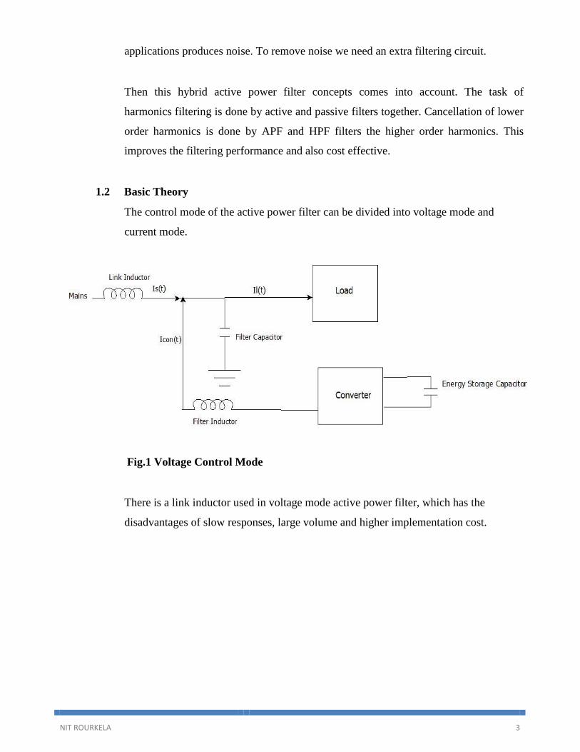
Fig.1 Voltage Control Mode
There is a link inductor used in voltage mode active power filter, which has the
disadvantages of slow responses, large volume and higher implementation cost.
Page 13
NIT ROURKELA 4
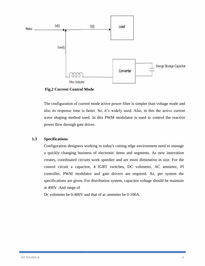
Fig.2 Current Control Mode
The configuration of current mode active power filter is simpler than voltage mode and
also its response time is faster. So, it’s widely used. Also, in this the active current
wave shaping method used. In this PWM modulator is used to control the reactive
power flow through gate driver.
1.3 Specifications
Configuration designers working in today's cutting edge environment need to manage
a quickly changing business of electronic items and segments. As new innovation
creates, coordinated circuits work speedier and are more diminutive in size. For the
control circuit a capacitor, 4 IGBT switches, DC voltmeter, AC ammeter, PI
controller, PWM modulator and gate drivers are required. As, per system the
specifications are given. For distribution system, capacitor voltage should be maintain
at 400V .And range of
Dc voltmeter be 0-400V and that of ac ammeter be 0-100A.
Page 14
NIT ROURKELA 5
CHAPTER 2
Background and Literature Review
2.1 Power Quality
2.2 Passive Filter
2.3 Active Power Filter
Page 15
NIT ROURKELA 6
2. Background and Literature Review 2.1 Power quality
Any power problem that results in failure or disoperation of customer equipment
manifests itself as an economic burden to the user, or produces negative impacts on the
environment. Any power problem that is due to voltage, current or frequency deviation
defines power quality. It also results in the failure of customer requirement. Poor power
quality can result in lost productivity, lost and corrupt data, damaged equipment and
early failure of equipment. There are three key aspects of power quality power factor,
harmonics and disturbance. Among these harmonic distortion is the most severe
problem. Harmonic distortion is mainly due to the electronic loads (i.e. nonlinear
loads). As a result, power conditioning equipments are becoming very essential for the
customer utilities. Then many equipments are developed to diminish this problem like
tuned passive filters, reactors etc. Active filters or active harmonics conditioners also
are used to compensate the harmonic power. For detection and classification of power
quality many researches and studies are being conducted. Many methods are being
developed like discrete Fourier transform, wavelet transform, data mining etc. Also,
active power filter is also a way to improve the power quality. With the help of these
disturbance in power quality can be detected and also this problem can be solved.
2.2 Passive Filter
Passive filters are of three types.
Single tuned filter
Damped filter
C-Type high pass filter
In single tuned filter, the quality factor is defined as Q = X0/R.
In damped filter, quality factor is defined as Q = 1/GX0
Where G is the conductance of the resistor in parallel with the inductor.
Quality factor defines the performance of the passive filters.
High pass filters are the second order damped filters. For the harmonics above 25th
order, this type of filter is used.
For high pass filter Q = R/X0, where X0 = (L/C)0.5.
If the reactive power supplied by the filter is increased, then filtering performance also
Page 16
NIT ROURKELA 7
improves.
Fig.3 Different Types of Passive Filter
2.3 Active Power Filter
An analog electronic filter is combined with the active components like Opamp, PWM
controllers etc. defines the active power filter. A filter is designed which leads to the
improvising of the performance, this is included in amplifiers and also this improves
the reliability of the filter. Also in these type of filters requirements of inductors
reduces due to which it becomes very cheap as compared to other components.
Characteristics of the filter remains unaffected because of the amplifier as it prevents
the load impedance. There is presence of complex poles and zeroes, even if no bulky
inductor is used. With use of variable resistors tuned frequency, quality factor and
response can be improvised. Some standard power quality problems can be fixed
through these active power filters. Hence, to improvise the power quality depends on
which type of active power filter we choose and that depends on the source of problem.
Types of Active power filter
1. Shunt Active Power Filters
2. Series Active Power Filters
Page 17
NIT ROURKELA 8
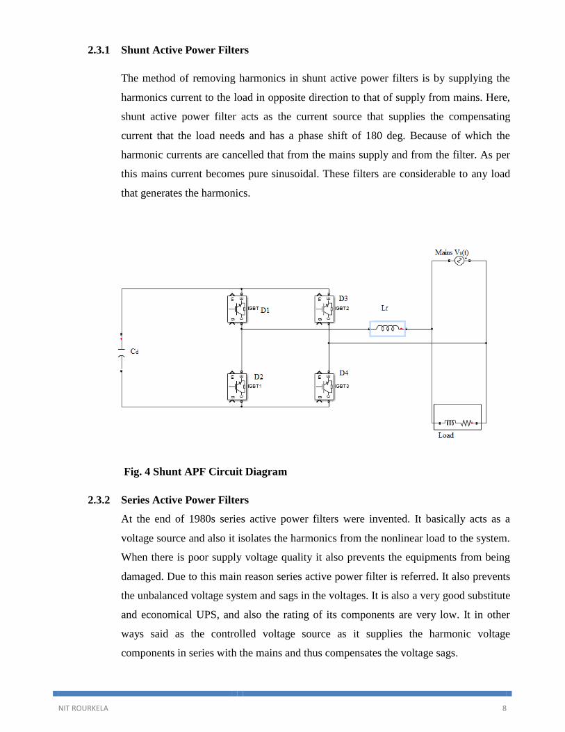
2.3.1 Shunt Active Power Filters
The method of removing harmonics in shunt active power filters is by supplying the
harmonics current to the load in opposite direction to that of supply from mains. Here,
shunt active power filter acts as the current source that supplies the compensating
current that the load needs and has a phase shift of 180 deg. Because of which the
harmonic currents are cancelled that from the mains supply and from the filter. As per
this mains current becomes pure sinusoidal. These filters are considerable to any load
that generates the harmonics.
Fig. 4 Shunt APF Circuit Diagram
2.3.2 Series Active Power Filters
At the end of 1980s series active power filters were invented. It basically acts as a
voltage source and also it isolates the harmonics from the nonlinear load to the system.
When there is poor supply voltage quality it also prevents the equipments from being
damaged. Due to this main reason series active power filter is referred. It also prevents
the unbalanced voltage system and sags in the voltages. It is also a very good substitute
and economical UPS, and also the rating of its components are very low. It in other
ways said as the controlled voltage source as it supplies the harmonic voltage
components in series with the mains and thus compensates the voltage sags.
Page 18
NIT ROURKELA 9
CHAPTER 3
METHODOLOGY
3.1 Design Procedures
3.1.1 Active power filter Configuration
3.1.2 Control Block Diagram
3.2 Component Calculations
3.3 Simulation Procedure
Page 19
NIT ROURKELA 10
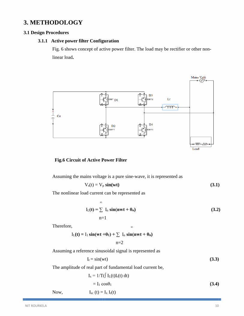
3. METHODOLOGY
3.1 Design Procedures
3.1.1 Active power filter Configuration
Fig. 6 shows concept of active power filter. The load may be rectifier or other non-
linear load.
Fig.6 Circuit of Active Power Filter
Assuming the mains voltage is a pure sine-wave, it is represented as
Vs(t) = Vp sin(wt) (3.1)
The nonlinear load current can be represented as
∞
IL(t) = ∑ In sin(nwt + θn) (3.2)
n=1
Therefore, ∞
IL(t) = I1 sin(wt +θ1) + ∑ In sin(nwt + θn)
n=2
Assuming a reference sinusoidal signal is represented as
Ir = sin(wt) (3.3)
The amplitude of real part of fundamental load current be,
Ix = 1/T(∫ IL(t)Ir(t) dt)
= I1 cosθ1 (3.4)
Now, Isc (t) = Ix Ir(t)
Page 20
NIT ROURKELA 11
= I1 cosθ1 sin(wt) (3.5)
Hence, calculated compensation current be,
Icr(t) = IL(t) – Isc(t) (3.6)
3.1.2 Component Functions
The inductor shown in Fig.6 is used to ensure that the compensation current
generated by the convertor is smooth current, an inductor is required to filter out the
switching ripple current. For a good dynamic response, the size of this inductor must
be as small as possible. If the inductor is too small, it cannot suppress the switching
ripple current. It may cause the problem of multi-crossing phenomenon because the
change rate of the convertor output current is larger than the slope of the triangle
carrier signal. This has the result that the switching frequency is higher than the
carrier signal frequency. In addition, the gain of the error amplifier can affect this
phenomenon. A PI controller is used to provide approximate amplitude to the mains
current. Square wave generator and then sine wave is generated from source for
synchronization. Now, the error signal is send to PWM modulator which is required
to give the gate pulses for compensation current. To PWM modulator carrier
waveform given is triangular wave and through this frequency of gate pulses can be
controlled. The load here should be non-linear.
3.2 Component Calculations
In order for the circuit to function properly, the external components need to be
calculated carefully. Voltage across the capacitor should be maintained more than 1.41
times of Vmains . For the PI controller,
Ki = (L + L0 ).wc / (2 * Vdc ) (3.7)
Kp = wc * Ki (3.8)
This equations stands for triangular wave of amplitude 1 peak to peak.
Where, L + L0 = Total inductance,
Wc = Triangular wave frequency
Vdc = Capacitor voltage
Page 21
NIT ROURKELA 12
3.3 Simulation Procedure
Figure 7 shows the exact circuit that was used in the Matlab simulation for full wave rectifier.
Fig.7 Matlab Simulation for Full Wave Rectifier
Page 22
NIT ROURKELA 13
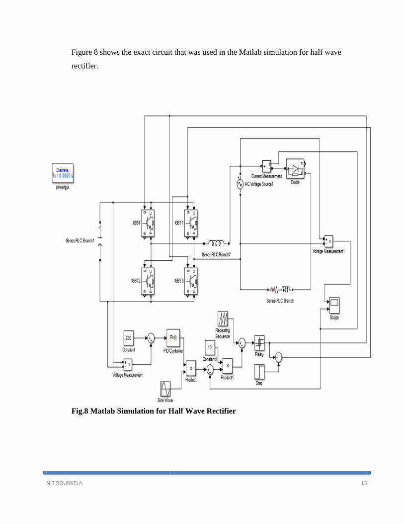
Figure 8 shows the exact circuit that was used in the Matlab simulation for half wave
rectifier.
Fig.8 Matlab Simulation for Half Wave Rectifier
Page 23
NIT ROURKELA 14
CHAPTER 4
SIMULATION RESULTS
Page 24
NIT ROURKELA 15
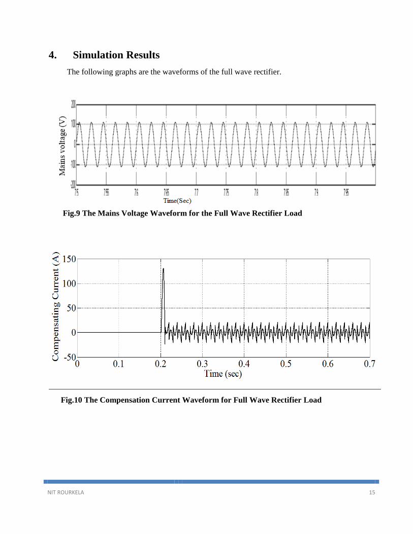
4. Simulation Results
The following graphs are the waveforms of the full wave rectifier.
Fig.9 The Mains Voltage Waveform for the Full Wave Rectifier Load
Fig.10 The Compensation Current Waveform for Full Wave Rectifier Load
Page 25
NIT ROURKELA 16
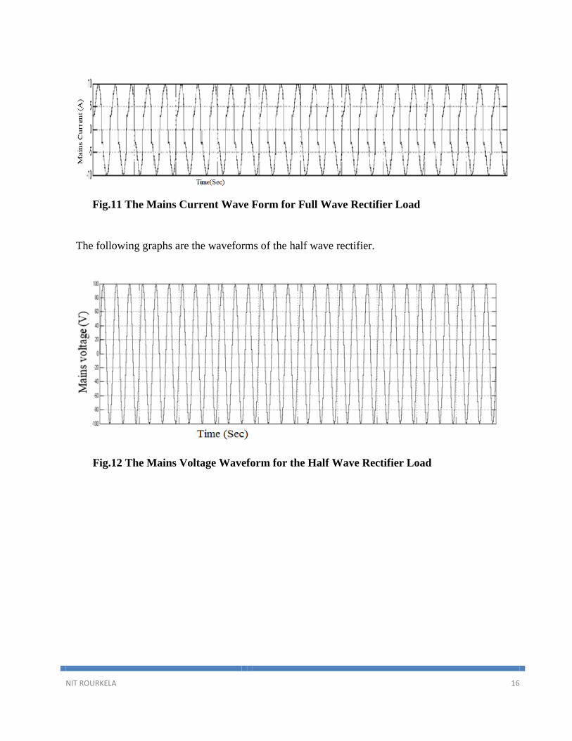
Fig.11 The Mains Current Wave Form for Full Wave Rectifier Load
The following graphs are the waveforms of the half wave rectifier.
Fig.12 The Mains Voltage Waveform for the Half Wave Rectifier Load
Page 26
NIT ROURKELA 17
Fig.13 The Mains Current Waveform for Half Wave Rectifier Load
Page 27
NIT ROURKELA 18
CHAPTER 5
Hardware Implementation
5.1 Component Description for Hardware Design
5.1.1 Single phase variac
5.1.2 IGBT based inverter
5.1.3 Single phase rectifier
5.1.4 Current Sensor
5.1.5 Voltage Sensor
5.1.6 Gate Driver
5.1.7 Filter inductor
Page 28
NIT ROURKELA 19
CHAPTER-5 :
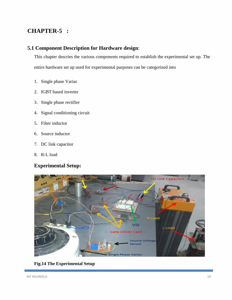
5.1 Component Description for Hardware design:
This chapter descries the various components required to establish the experimental set up. The
entire hardware set up used for experimental purposes can be categorized into
1. Single phase Variac
2. IGBT based inverter
3. Single phase rectifier
4. Signal conditioning circuit
5. Filter inductor
6. Source inductor
7. DC link capacitor
8. R-L load
Experimental Setup:
Fig.14 The Experimental Setup
Page 29
NIT ROURKELA 20
5.1.1 Single Phase Variac
It was used to provide supplied voltage of 230 Volt (r.m.s) required for experimental
set up.
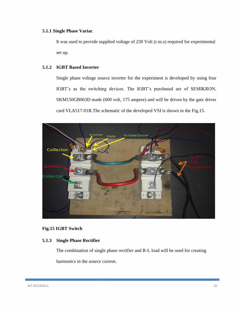
5.1.2 IGBT Based Inverter
Single phase voltage source inverter for the experiment is developed by using four
IGBT’s as the switching devices. The IGBT’s purchased are of SEMIKRON,
SKM150GB063D made (600 volt, 175 ampere) and will be driven by the gate driver
card VLA517-01R.The schematic of the developed VSI is shown in the Fig.15.
Fig.15 IGBT Switch
5.1.3 Single Phase Rectifier
The combination of single phase rectifier and R-L load will be used for creating
harmonics in the source current.
Page 30
NIT ROURKELA 21
5.1.4 Current Sensor
For the control scheme, source current and load current have to be sensed. Two
LEM manufactured current transducers LA 55-P, will be used to sense respective
currents.
The schematic of current sensor is shown in Fig.16.
Fig.16 Schematics of the Current Sensor
The magnetic flux created by the primary current is balanced through a secondary coil
using Hall device and associated electronic circuit.
Fig.19 Circuit of Current Sensor
Page 31
NIT ROURKELA 22
The number of secondary turns (Ns) is 1000 and the maximum value of secondary
current (Is) is 50mA. Primary current (Ip) is the current that is to be measured. The
magnetic flux created by the primary current is balanced through a secondary coil
using a Hall device and associated electronic circuit. The relation given by the
following Equation holds true during operation.
Np×Ip=Ns×Is
Where, Np is number of primary turns. In the experiment, Np = 1, thus a primary
current up to 50A can be safely measured. Since the turn ratio is constant, the
secondary current is an exact representation of the primary current. The output signal
is the voltage drop on the resistance Rm caused by the secondary current. A 100Ω
resistance is selected as Rm. This output signal needs to be scaled within the analog
input limits (-10V to +10V) of data acquisition card, which is done by a non-
inverting opamp configuration. Two variable resistances, Ri and Rf, are used to
select a proper gain. The current sensor and opamp both require ±15V supply for
their operation which is provided by DC power supply module. It is then calibrated
to find the exact relation between input current and output voltage.
Two current sensor cards are required for sensing
1. Source current
2. Load current
Page 32
NIT ROURKELA 23
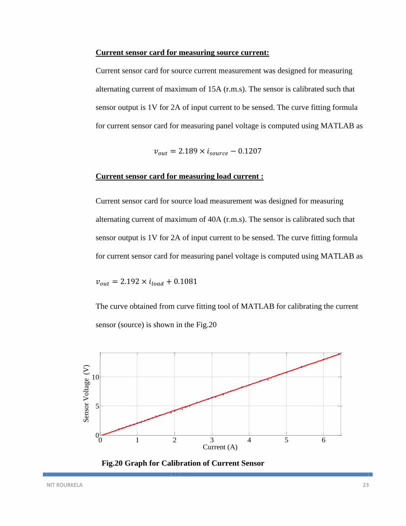
Current sensor card for measuring source current:
Current sensor card for source current measurement was designed for measuring
alternating current of maximum of 15A (r.m.s). The sensor is calibrated such that
sensor output is 1V for 2A of input current to be sensed. The curve fitting formula
for current sensor card for measuring panel voltage is computed using MATLAB as
𝑣𝑜𝑢𝑡 = 2.189 × 𝑖𝑠𝑜𝑢𝑟𝑐𝑒 − 0.1207
Current sensor card for measuring load current :
Current sensor card for source load measurement was designed for measuring
alternating current of maximum of 40A (r.m.s). The sensor is calibrated such that
sensor output is 1V for 2A of input current to be sensed. The curve fitting formula
for current sensor card for measuring panel voltage is computed using MATLAB as
𝑣𝑜𝑢𝑡 = 2.192 × 𝑖𝑙𝑜𝑎𝑑 + 0.1081
The curve obtained from curve fitting tool of MATLAB for calibrating the current
sensor (source) is shown in the Fig.20
Fig.20 Graph for Calibration of Current Sensor
0 1 2 3 4 5 60
5
10
Current (A)
Sen
sor
Vo
ltag
e (
V)
Page 33
NIT ROURKELA 24
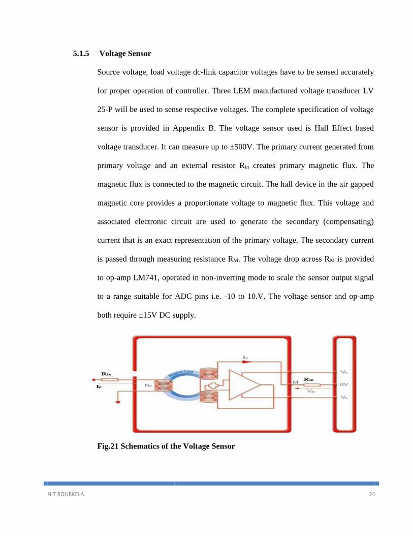
5.1.5 Voltage Sensor
Source voltage, load voltage dc-link capacitor voltages have to be sensed accurately
for proper operation of controller. Three LEM manufactured voltage transducer LV
25-P will be used to sense respective voltages. The complete specification of voltage
sensor is provided in Appendix B. The voltage sensor used is Hall Effect based
voltage transducer. It can measure up to ±500V. The primary current generated from
primary voltage and an external resistor Rin creates primary magnetic flux. The
magnetic flux is connected to the magnetic circuit. The hall device in the air gapped
magnetic core provides a proportionate voltage to magnetic flux. This voltage and
associated electronic circuit are used to generate the secondary (compensating)
current that is an exact representation of the primary voltage. The secondary current
is passed through measuring resistance RM. The voltage drop across RM is provided
to op-amp LM741, operated in non-inverting mode to scale the sensor output signal
to a range suitable for ADC pins i.e. -10 to 10.V. The voltage sensor and op-amp
both require ±15V DC supply.
Fig.21 Schematics of the Voltage Sensor
Page 34
NIT ROURKELA 25
Fig.22 Hardware Circuit for Voltage Sensor
The curve fitting formulas for three voltage sensors are computed as
For source voltage sensor, 𝑣𝑜𝑢𝑡 = 0.0923 × 𝑣𝑠𝑜𝑢𝑟𝑐𝑒 + 0.2380
For load voltage sensor, 𝑣𝑜𝑢𝑡 = 0.0904 × 𝑣𝑙𝑜𝑎𝑑 + 0.2541
For DC link voltage sensor, 𝑣𝑜𝑢𝑡 = 0.0941 × 𝑣𝐷𝐶_𝑙𝑖𝑛𝑘 + 0.3541
Fig.23 Graph for Calibration for Voltage Sensor
10 20 30 40 50 60 70 80 90 100
2
4
6
8
10
Voltage (V)
Sen
sor
Ou
tpu
t V
olt
age
(V)
Page 35
NIT ROURKELA 26
5.1.6 Gate Driver
High performance FUJI’s hybrid IGBT driver IC, VLA517-01R will be used to
provide the necessary driving signals to the IGBT across the gate emitter terminals.
This hybrid IC is a circuit designed for driving n-channel IGBT modules. An
optocoupler is used in this chip to provide the required isolation between the signal
side of the chip and the power side. The input to the chip is a digital signal of +5V as
logic high and 0V as logic low and the corresponding outputs are +15V and -5V.
Output of this chip is connected through a proper gate series resistance (Rg=25Ω)
across the gate emitter terminals of the corresponding IGBT, which is to be driven.
The input logic signal given to the chip should be capable of driving a current of
10mA for the satisfactory operation of this chip. The circuit diagram implemented in
the present work for the IGBT driver is shown in Fig.22.
Fig.22 Schematics of the Gate Driver Circuit
Page 36
NIT ROURKELA 27
Fig.23 Hardware Circuit for Gate Driver
Fig.24 The Output of Gate Driver on CRO
5.1.7 Filter Inductor
The purpose of using filter inductor is to eliminate very high frequency component
from filter injected current.
Page 37
NIT ROURKELA 28
CHAPTER 6
CONCLUSIONS
Page 38
NIT ROURKELA 29
6. Conclusions
By using appropriate value of Ki and Kp with error amplifier and PWM modulator the
reactive power can be provided through capacitor. Hence minimizing the harmonics
and improving the power factor. And using passive high pass filter in parallel with
proper Rh , Lh and capacitance (Ch)value harmonics can be minimized. This simulation
is to be verified through the experimental setup but due to failure of the setup, results
shown are of simulation outputs. From the simulation results it is concluded that it is
very important to remove harmonics and active power filter makes it possible in well-
mannered way. This also provides the reactive power compensation.
Future Scope for Further Research
With the use of DAQ card and the DC supply the setup will be completed and then the
simulation results can be verified. With this the research can be concluded that active power
filter is very good method for compensation of harmonics and also a very well and
improvised method for the reactive power compensation.
Page 39
NIT ROURKELA 30
REFERENCES
[1] J.C.Wu and H.L.Jou , “Simplified control method for the single phase active power
Filter”, Vol. 143, No. 3, May 1996
[2] H.L.jou and J.C.Wu and H.Y.Chu, “New single phase active power filter”, Vol. 141,
No.3, May 1994
[3] H. Rudnick, J.Dixon and L.Moran, “Active power filters as a solution to power-
quality problems in distribution networks,” IEEE Power and Energy Magazine.
[4] R. C. Dugan, M. F. McGranaghan, S. Santoso and H. W. Beaty, “Electrical Power
Systems Quality,” 2nd ed. USA: McGraw-Hill, 2002
[5] S. Fukuda and T. Endoh, “Control Method for a Combined Active Filter System
Employing a Current Source Converter and a High Pass Filter”, IEEE Trans. On Industry
Application, Vol. 31
[6] Gourishankar Mishra, “Design of Passive High Pass Filter for Hybrid Active Power Filter
Applications”, from ethesis.nitrkl.ac.in
[7] Power Electronics Handbook by M.H.Rashid. 2nd edition
[8] Akagi, H. New Trends in Active Filters for Power Conditioning. IEEE Trans. on Industry
Application 1996. 32(6): 1312-1322
Page 40
NIT ROURKELA 31
[9] Ghosh, A. and Ledwich, G., Power Quality Enhancement Using Custom Power Devices.
Massachusetts, USA: Kluwer Academic Publishers. 2002
[10] Phipps, J. K. A Transfer Function Approach to Harmonic Filter Design. IEEE Industry
application Magazine.1997.3 (2): 68-82
[11] Dugan, R. C., McGranaghan, M.F., Santoso, S., and Beaty, H. W. Electrical Power
Systems Quality. 2nd. Ed. USA: McGraw-Hill. 2002.