IEEE TRANSACTIONS ON ELECTRON DEVICES, VOL. 39, NO. 9, SEPTEMBER 1992 2099 Study of the Growth Temperature Dependence of Performance and Reliability of Thin MOS Gate Oxides Aniruddha B. Joshi, Student Member, IEEE, and Dim-Lee Kwong, Senior Member, IEEE Abstract-An in-depth and systematic investigation is carried out to find the role of oxide growth temperature in determining the quality of the resulting gate oxide in MOS devices. Perfor- mance of fresh devices as well as degradation under hot-carrier stress and radiation exposure are studied using MOS capacitors and MOSFET’s. Experimental results indicated that better charge trapping properties and interface endurance to both hot carrier-stress and ionizing radiation can be realized by elevat- ing the gate oxidation temperature. Substantial experimental evidence is provided to establish that interface state generation during stress is mainly responsible for the degradation of var- ious MOSFET parameters. These findings point out that rapid thermal processing may be the technique for the growth of ultrathin gate oxides for deep-submicrometer MOS technology, at least from the quality and reliability point of view. I. INTRODUCTION CALING of gate oxide thickness has become inevi- S table as the MOSFET channel lengths are reduced, in order to eliminate the undesirable short-channel effects such as charge sharing and drain-induced barrier lower- ing. A tight control over oxide growth is essential to pre- vent even small deviations from the desired oxide thick- ness which can cause significant deviations in device performance in the sub-10-nm regime. Such control is achieved by lowering the thermal budget of the process. When this approach is adopted, it is necessary to study the effect of the oxidation temperature on the quality of the resulting oxide in terms of device performance and reliability under hot-carrier stress. There have been a few studies in the past to investigate the effects of gate oxide growth temperature on the quality of the devices [1]-[3]. Hahn and Henzler [l] studied the structural and electrical properties of the Si02/Si inter- face as a function of oxidation temperature. They reported a strong correlation between the atomic steps at the inter- face, which were taken as a measure of roughness, and the electrical properties and found out that high-temper- ature oxidation results in a smoother interface with less Manuscript received August 15, 1991; revised February 12, 1992. This work was partially supported by SRCBEATECH under Contract SRC88MC505 and by the Texas Advanced Technology Program. The re- view of this paper was arranged by Associate Editor Y. Nishi. The authors are with the Microelectronics Research Center, Department of Electrical and Computer Engineering, The University of Texas at Aus- tin, Austin, TX 78712. IEEE Log Number 9201802. interface states and less fixed charge. Nulman el al. [2] reported that oxides grown at 1150°C using rapid thermal processing show less trap generation under Fowler- Nordheim (F-N) stress, as compared to the furnace oxides grown at 850°C. On the contrary, Sakashita et al. [3] re- cently preferred a low-temperature gate oxidation to re- duce positive charge generation during F-N stress. There is, however, no study which reports the effect of gate ox- ide growth temperature on the properties of as fabricated MOSFET’s and the degradation of MOSFET’s under stress. In this work we address this important issue of the effect of oxidation temperature on performance and reli- ability of thin oxide (- 11 nm) MOSFET’s. 11. EXPERIMENTAL DETAILS The MOS devices with LOCOS isolation were fabri- cated on (100) p-type substrates with a resistivity of 1-2 Q - cm. After active area definition steps, thin ( - 11 nm) Si02 films were grown in dry O2 ambient at different tem- peratures followed by a 15 min N2 anneal. Gate electrodes were formed by the deposition of 4000-A phosphorus- doped polysilicon. Source/drain junctions for n-MOS- FET’s were formed by arsenic implant and the estimated junction depth was 0.25 pm. A final sinter was performed at 400°C in forming gas. MOS capacitors with a gate area of 1 x cm2 and MOSFET’s with W/L ratio of 25 pm/2 pm were used in this work. Flatband voltage ( Vbf) and interface state densities (Dit) of MOS capacitors were obtained from high-frequency and quasi-static capacitance-voltage (C-V) characteris- tics [4]. Fowler-Nordheim (F-N) injection was performed on MOS capacitors with negative gate bias. The changes in the interface state density resulting from this injection were estimated using C-V techniques. Changes in gate voltage (AV,) in order to maintain constant gate current (Ig) during the injection were monitored to study the charge trapping properties of the oxide films. Fresh MOSFET’s were characterized to extract the conventional parameters such as threshold voltage ( V,), transconductance (Gm), and subthreshold swing (S), at Vd = 50 mV. Due to the absence of channel implant, the V, ranged between 0.02 to 0.04 V. This variation showed no trend with the oxidation temperature. Effective carrier mobility was extracted from Zd-Vg characteristics [5]. Off- 0018-9383/92$03.00 0 1992 IEEE
Transcript
IEEE TRANSACTIONS ON ELECTRON DEVICES, VOL. 39, NO. 9, SEPTEMBER 1992 2099
Study of the Growth Temperature Dependence of Performance and Reliability of Thin
MOS Gate Oxides Aniruddha B . Joshi, Student Member, IEEE, and Dim-Lee Kwong, Senior Member, IEEE
Abstract-An in-depth and systematic investigation is carried out to find the role of oxide growth temperature in determining the quality of the resulting gate oxide in MOS devices. Perfor- mance of fresh devices as well as degradation under hot-carrier stress and radiation exposure are studied using MOS capacitors and MOSFET’s. Experimental results indicated that better charge trapping properties and interface endurance to both hot carrier-stress and ionizing radiation can be realized by elevat- ing the gate oxidation temperature. Substantial experimental evidence is provided to establish that interface state generation during stress is mainly responsible for the degradation of var- ious MOSFET parameters. These findings point out that rapid thermal processing may be the technique for the growth of ultrathin gate oxides for deep-submicrometer MOS technology, at least from the quality and reliability point of view.
I. INTRODUCTION CALING of gate oxide thickness has become inevi- S table as the MOSFET channel lengths are reduced, in
order to eliminate the undesirable short-channel effects such as charge sharing and drain-induced barrier lower- ing. A tight control over oxide growth is essential to pre- vent even small deviations from the desired oxide thick- ness which can cause significant deviations in device performance in the sub-10-nm regime. Such control is achieved by lowering the thermal budget of the process. When this approach is adopted, it is necessary to study the effect of the oxidation temperature on the quality of the resulting oxide in terms of device performance and reliability under hot-carrier stress.
There have been a few studies in the past to investigate the effects of gate oxide growth temperature on the quality of the devices [1]-[3]. Hahn and Henzler [ l ] studied the structural and electrical properties of the Si02/Si inter- face as a function of oxidation temperature. They reported a strong correlation between the atomic steps at the inter- face, which were taken as a measure of roughness, and the electrical properties and found out that high-temper- ature oxidation results in a smoother interface with less
Manuscript received August 15, 1991; revised February 12, 1992. This work was partially supported by SRCBEATECH under Contract SRC88MC505 and by the Texas Advanced Technology Program. The re- view of this paper was arranged by Associate Editor Y. Nishi.
The authors are with the Microelectronics Research Center, Department of Electrical and Computer Engineering, The University of Texas at Aus- tin, Austin, TX 78712.
IEEE Log Number 9201 802.
interface states and less fixed charge. Nulman el al. [2] reported that oxides grown at 1150°C using rapid thermal processing show less trap generation under Fowler- Nordheim (F-N) stress, as compared to the furnace oxides grown at 850°C. On the contrary, Sakashita et al. [3] re- cently preferred a low-temperature gate oxidation to re- duce positive charge generation during F-N stress. There is, however, no study which reports the effect of gate ox- ide growth temperature on the properties of as fabricated MOSFET’s and the degradation of MOSFET’s under stress. In this work we address this important issue of the effect of oxidation temperature on performance and reli- ability of thin oxide ( - 11 nm) MOSFET’s.
11. EXPERIMENTAL DETAILS The MOS devices with LOCOS isolation were fabri-
cated on (100) p-type substrates with a resistivity of 1-2 Q - cm. After active area definition steps, thin ( - 11 nm) Si02 films were grown in dry O2 ambient at different tem- peratures followed by a 15 min N2 anneal. Gate electrodes were formed by the deposition of 4000-A phosphorus- doped polysilicon. Source/drain junctions for n-MOS- FET’s were formed by arsenic implant and the estimated junction depth was 0.25 pm. A final sinter was performed at 400°C in forming gas. MOS capacitors with a gate area of 1 x cm2 and MOSFET’s with W / L ratio of 25 pm/2 pm were used in this work.
Flatband voltage ( Vbf) and interface state densities (Dit) of MOS capacitors were obtained from high-frequency and quasi-static capacitance-voltage (C-V) characteris- tics [4]. Fowler-Nordheim (F-N) injection was performed on MOS capacitors with negative gate bias. The changes in the interface state density resulting from this injection were estimated using C-V techniques. Changes in gate voltage (AV,) in order to maintain constant gate current (Ig) during the injection were monitored to study the charge trapping properties of the oxide films.
Fresh MOSFET’s were characterized to extract the conventional parameters such as threshold voltage ( V,), transconductance (Gm), and subthreshold swing (S), at Vd = 50 mV. Due to the absence of channel implant, the V, ranged between 0.02 to 0.04 V. This variation showed no trend with the oxidation temperature. Effective carrier mobility was extracted from Zd-Vg characteristics [5]. Off-
0018-9383/92$03.00 0 1992 IEEE
2100 IEEE TRANSACTIONS ON ELECTRON DEVICES, VOL. 39, NO. 9, SEPTEMBER 1992
state leakage current ( Id l ) was obtained with the channel turned off and with Vd = 5 V applied. Charge pumping measurements [6] were performed on the MOSFET’s to estimate D;, using a triangular pulse with a frequency of 100 kHz and amplitude of 4 V.
Constant-current F-N stress was performed on MOS capacitors at - 1 mA/cm2, which was obtained at an ox- ide field of - 10 mV/cm. MOSFET’s were stressed at Vd = 7.5 V at peak substrate current condition. Channel hot- electron stress (CHES) was performed for lo4 s and the resulting changes in interface state density (AD,,), subthreshold swing (AS), transconductance (AG,,e,k/ Gm.peak (0)) and off-state leakage current (AId,) were mon- itored using the techniques described earlier. To deter- mine the degradation mode in MOSFET’s, AG, was stud- ied as a function of stress time in a set of devices. A set of MOS capacitors and MOSFET’s with different gate ox- idation temperatures was exposed to 50-keV X-rays to a dose of 0.5 Mrad and the resulting changes in device parameters were studied using the methods described above.
111. EFFECTS OF GATE OXIDE GROWTH TEMPERATURE ON THE CHARACTERISTICS OF MOS CAPACITORS A N D
MOSFET’s A. MOS Capacitor Characteristics
Characteristics of the as-fabricated MOS capacitors are summarized in Fig. 1. The high-frequency C-V curves for MOS capacitors with gate oxides grown at various tem- peratures showed little dependence on growth tempera- ture [7]. All the capacitors were found to have Vrr, - -0.95 V. From quasi-static C-Vcharacteristics, mid-gap interface state density (Dj,-,) was obtained for various samples and was found to be close to 2 x 10” eV-’ . cm-2, irrespective of the oxidation temperature as seen from Fig. 1. From the Ig-Vg characteristics of different MOS capacitors, the current in the F-N tunneling regime was observed to be independent of growth temperature. From these curves, the F-N curves were calculated and the value of parameter “B” in the equation J = A . E:x * exp (-B/Eo,) was obtained to be -21 MV/cm. From this, the barrier height was estimated to be 3.0 eV, inde- pendent of the growth temperature.
B. MOSFET Characteristics Fig. 2(a) show the channel current (Id) in the MOS-
FET’s, normalized with respect to gate oxide capacitance (Cox) , with different gate oxidation temperatures for Vd = 5 V. For both low and high gate drive we observed an increase in Id with increase in oxidation temperature. It should be noted that the increase is more prominent for higher gate drive. G,, normalized with respect to CO,, also shows a dramatic improvement with increasing oxidation temperature for high gate drive as shown in Fig. 2(b).
Effective electron mobility, defined as peff = I d / [ V d W / L * Cox(Vg - V d ] , is plotted in Fig. 3 as a function of effective normal field (Eeff). It is seen that peff increases
2.0 ’ O.%
c ? 0.94
0.90 0.0 100 800 900 1000 1100 12UU
Temperature (“C)
Fig. 1 . Flatband voltage and midgap interface state density in as-fabri- cated MOS capacitors obtained from high-frequency and quasi-static C- V curves. The characteristics show little dependence on the oxidation tem- perature
1000°C I - 1100°C
O L I
0 1 2 3 4
Vg-VI (V)
(b)
Fig. 2. (a) Drain current (I,) and (b) transconductance (G,,,) normalized with respect to the oxide capacitance (Cox) plotted as a function of gate drive (V, - VT). The increase in both these quantities with oxidation tem- perature is more prominent at higher gate drive.
with increasing growth temperature, especially in the high Eeff regime, e.g., 0.6-0.8 MV/cm. In addition, peff in MOSFET’s with 900°C oxide show a weaker field depen- dence compared to those with 800°C oxide. For temper- atures higher than 900”C, the curves show a parallel shift over a wide Eeff range. It has been indicated that the roll- off of carrier mobility for higher gate drive is primarily caused by surface roughness scattering [5]. Therefore, the weaker field dependence of peff indicates a smoother Si02/Si interface.
JOSH1 AND KWONG: PERFORMANCE AND RELIABILITY OF THIN MOS ( ;ATE OXIDES 2101
I A'. I
500 - h
U a4 'f * .
N
400- v
! 300 -
1000°C 1100°C - - - -
200 --.. ' I 1 0.0 0.2 0.4 0.6 0.8 1.0
Eerr (MVlcm) Fig. 3 . Effective electron mobility (peff ) versus effective electric field (Eeff)
in MOSFET's with gate oxides grown at different temperatures.
As indicated by Sun and Plummer [5] , high-field carrier mobility is mainly determined by roughness scattering and phonon scattering. Since all the devices under study are operated at the same temperature, the observed variation in effective carrier mobility is most likely due to different amounts of roughness scattering in these samples. Thus our results indicate that the interface roughness is reduced when the oxidation is carried out at higher temperatures and, thereby, support the conclusions of Hahn and Henzler [ l ] who proposed a two-factor model to account for the increase in interface smoothness at higher growth temperature. According to their model, random oxidation reaction increases interface roughness, whereas diffusion of oxidizing specie across the interface causes interface smoothing. The final roughness is govemed by the bal- ance of these two processes. As the oxidation temperature is increased, there is an enhanced diffusion of the oxidiz- ing specie across the interface, which results in a smoother interface, as reflected in our studies. As revealed by MOS capacitor studies, no noticeable variation of fixed charge and Dit was observed as a function of growth temperature. Therefore, we cannot attribute the changes in low-field peff to changes in Coulombic scattering [ 5 ] . Since these changes are smaller than those in high-field peff, we sus- pect that the interface roughness scattering is responsible for them, but the influence is weaker than that on high- field p e f f .
For other quantities under study such as S and Id,, we did not observe any significant variation with the changes in oxidation temperature. Since S is related to the inter- face state density, lack of dependence of S on oxidation temperature is in agreement with the observations on fresh MOS capacitors. This was further confirmed by charge pumping measurements on the MOSFET's. Id, has been attributed to band-to-band (B-B) tunneling of electrons in
the corner region under the gate-drain overlap [8] and has been shown to strongly depend on the surface field (E,). Since there was little variation observed in oxide fixed charge or D;, in fresh MOS capacitors with different gate oxidation temperatures, we expect little variations in E, and, therefore, Zdl .
IV. EFFECT OF GATE OXIDATION TEMPERATURE ON
STRESS RESPONSE OF MOS CAPACITORS AND MOSFET's
A . Constant Current F-N Stressing of MOS Capacitors Unlike the properties of as-fabricated MOS capacitors,
the degradation under stress was observed to have a strong dependence on oxidation temperature.
Fig. 4 shows the changes in V, necessary to maintain a constant current density of -1 mA/cm2 with the gate biased at a negative voltage. All the samples indicate an initial brief period of hole trapping as shown by the re- duction in gate bias to maintain the constant current. The 1100°C sample shows the maximum hole trapping, whereas it was of comparable magnitude in the other two samples. Since the F-N tunneling currents are of compa- rable magnitude in all the three samples, the cathode and anode fields in this initial phase are identical in all the three samples. The higher hole trapping in the 1100°C sample is, therefore, most likely due to the higher density of hole traps in that sample. It is generally accepted that oxygen vacancy (03 = Si * ) in the Si-0 network acts as a hole traps [4]. Since higher growth temperatures led to higher oxidation rates, the 1100°C sample is likely to have a higher density of hole traps [9] which is consistent with our observations.
All the samples show electron trapping after this brief hole trapping phase, as seen by more positive gate volt- ages necessary to maintain the constant current. It is ob- served that more AV, is required to offset the changes in the cathode field caused by charge trapping in the oxide with lower growth temperature. The electron trapping in these oxide films could be either due to the pre-existing traps in the oxide, as a result of processing, or traps cre- ated in the oxide during the stress. A recent study has indicated that intrinsic defect density in MOS-devices re- duces with the increase in growth temperature [ 101. From our present data, however, we cannot determine the con- tribution of these intrinsic defects to the net electron trap- ping.
Allit-,,, is strongly reduced in the MOS capacitors with high-temperature gate oxide. As can be seen from Fig. 5, ADit-,,, reduction is sharper as the growth temperature is increased between 900 to 1OOO"C than the decrease there- after. Since the interface state generation is closely re- lated to the density of strained bonds at the interface, we believe that the growth temperature plays an important in modifying the strain near the Si /Si02 interface. It has been reported earlier [ 1 I] that the oxide behaves as a vis- cous fluid above 960°C. We suspect that our observations have a close relationship with this phenomenon.
2 102 IEEE TRANSACTIONS ON ELECTRON DEVICES, VOL. 39, NO. 9, SEPTEMBER 1992
-L4U 0 150 300 450 600
STRESS TIME (s)
Fig. 4. Changes in gate voltage (AV,) required to maintain a constant cur- rent density of - 1 mA/cm2 across the MOS capacitors with gate oxides grown at different temperatures. More electron trapping is observed in ox- ides grown at lower temperatures.
Stress @ -1mAlcmz. 300 s
800 900 1000 1100 1200 Temperature ("C)
Fig. 5 . Changes in mid-gap interface state density (AD,,.,,,) resulting from gate injection for 300 s at a current density of - 1 mA/cm*, plotted as a function of gate oxidation temperature. Note the sharper decrease in AD,,.,,, in the 900 to 1OOO"C range.
B. Channel Hot Electron Stressing of MOSFETS As mentioned earlier, MOSFET's were stressed at a
condition so as to achieve the worst case degradation. AGm-Fak/Gm-peak(0) and AS are plotted in Fig. 6 versus the oxidation temperature. Both these quantities are sup- pressed for high-temperature oxidation, similar to our ob- servations on MOS capacitors under F-N stress. Since
AS, and AGm,eak/Gm,e,k(0) show a similar de- pendence on oxidation temperature, we suspect that these two quantities are closely related. To clarify this, we have plotted AGm.Fak / Gm.peak(0) versus ADir., in Fig. 7. Also shown in Fig. 7 is a correlation between AS and ADir-,. The strong linear correlations observed between these quantities suggest that interface state generation is a dom- inant degradation mechanism in the devices under study.
The peak substrate current condition results in injection of both electrons and holes in the oxide [12]. This con- dition leads to maximum interface state generation [ 131 as against charge trapping, which dominates under peak gate current [ 141. This is consistent with the strong correlation between AGm-peak / Gm-peak(O) As, and A&.
In Fig. 8, we plot AIdl as a function of oxidation tem- perature. To accentuate the similarity between the deg- radation of on-state and off-state parameters under stress, we have also included AGm-Fak/Gm-Fak(o) in Fig. 8. Sim- ilar to AGm.peak / Gm.peak(0) and AS, high-temperature ox- ide MOSFET's are observed to suffer less Id/ enhancement
0.07 ' 800 900 1000 1100 1200
Temperature ("C)
Fig. 6. Normalized transconductance degradation (AGm.Fak/Gm.Fak(o)) and changes in subthreshold swing (AS) as a function of gate oxide growth temperature. High-temperature oxidation results in suppressed device deg- radation under CHES in terms of both these quantities.
4 6 8 10 12 14 16 18 0.07' " ' " ' " . ' . " I-1
ADitSm (x1O10eV-1cmq2)
Fig. 7. Correlation between different on-state degradation measures. An excellent correlation indicates that the degradation is in terms of interface state generation as determined by our stressing conditions.
0.10 I 140
0.07' ' ' . ' ' ' ' ' 0 a00 900 1000 1100 12Uu
TEMPERATURE ("C)
Fig. 8. Increase in off-state leakage current (AI,,,) as a function of growth temperature. The leakage current is measured with the channel turned off and V,, = 5 V applied. Also shown is percentage transconductance degra- dation.
Id/ also known as gate-induced drain leakage (GIDL), is a result of B-B tunneling in the deeply depleted comer region under gate-drain overlap. In addition to B-B tun- neling [8], band-to-defect tunneling promoted by the in- terface states [ 151 and increased surface generation caused by a high Di, [ 161 are suggested to contribute to Id/. Since our stress conditions are desired to have little charge trap- ping in the oxide, the increase in Id/ can be attributed to the increase in D;, resulting from CHES. This speculation was corroborated by the excellent correlation between ALlir and AZd, as shown in Fig. 9. The figure also shows the correlation between mi, and the on-state parameter degradation (AGm-Fak / Gm-Fak(0)).
In this section, we have seen that the degradation of on-state (S, G,) and off-state (Id/) MOSFET parameters is dominated by interface state generation, due to the stress conditions used in this work. Furthermore, gate oxidation
JOSH1 AND KWONG: PERFORMANCE AND RELIABILITY OF THIN MOS GATE OXIDES
Fig. 9. A correlation between on-state (AG,,.Fak/G,,~Fak(0)) and off-state (AId,) parameters and ADi, (from charge pumping current data) indicating that the degradation is mainly caused by interface state generation from CHES.
at higher temperature reduces the degradation resulting from stress. Since strain in the interfacial region plays an important role in the interface state generation process, it can be concluded that variations in this strain due to dif- ferent growth temperatures are responsible for altering the hot carrier immunity of the MOS device.
v. INVESTIGATION OF THE DEGRADATION MECHANISM I N MOSFET’s
As reported in the previous section, an excellent cor- relation exists between the degradation and A D , esti- mated from the charge pumping measurements, in agree- ment with previous studies [17], [18]. In this section, we provide additional experimental results to confirm that SiO,/Si interface endurance to hot carrier stress is con- tinuously improved with the increase in growth tempera- ture.
A. Stress Time Dependence of Transconductance Degradation
Although G, degradation is important from a circuit designer’s viewpoint, investigation of the cause for this degradation in terms of more fundamental properties such as charge trapping and/or interface state generation is cru- cial in order to engineer the device fabrication. The cause for degradation has often been studied using two-distinct approaches. In one approach, degradation of various pa- rameters such as G, and V , is studied as a function of gate bias used for stressing and this dependence is com- pared with the substrate and gate current dependence on gate bias [14], [17], [19]. Alternatively, the stress time dependence of the degradation is investigated which can be expressed as a power law dependence on time [14], [17], [19], [20]. The exponent of this power law depen- dence is used to characterize the type of degradation in the device [14], [21]. The exponent ranging between 0.5 and 0.7 has been shown to be characteristic of interface state generation, where as a lower exponent (0.2-0.3) is a signature for charge trapping. The equivalence between these two approaches is shown in [ 141, [20].
We have used the second approach to study the primary degradation mechanism in our experiment. As before, MOSFET’s with gate oxides grown at different tempera-
2103
tures were stressed at peak substrate current condition, AGm.peak was monitored as a function of stress time. The substrate currents were of comparable magnitude in these devices. This was anticipated because the peak lateral electric field [19] for a particular gate and drain bias is the same in these devices due to the identical geometry. The slight difference in the substrate current was due to the changes in drain current due to the mobility variation, as observed in an earlier section. This similarity in the magnitude of substrate current enabled a fair comparison between different MOSFET’s.
Results of the above experiments are depicted in Fig. 10. Percentage decrease in Gm.peak is plotted versus stress time on a log-log scale. The data can be fit by a power law dependence [14], [17], [20] described as
AGm-peak /Gm-peak(O) = At”- (1)
The exponent “n” was estimated to range between 0.52 and 0.58, indicating interface state generation to be the dominant degradation in all three devices [14], in agree- ment with the correlation between AG, and AD, , men- tioned in an earlier section.
As seen from ( l ) , the parameter “A” provides parallel shifts of the log-log degradation versus time plots, as ob- served for the three devices in Fig. 10. Thus the param- eter “A” is associated with the gate oxide growth tem- perature. Higher growth temperature reduces “A” to give smaller interface state generation, which gives smaller transconductance degradation in the corresponding MOS- FET’s.
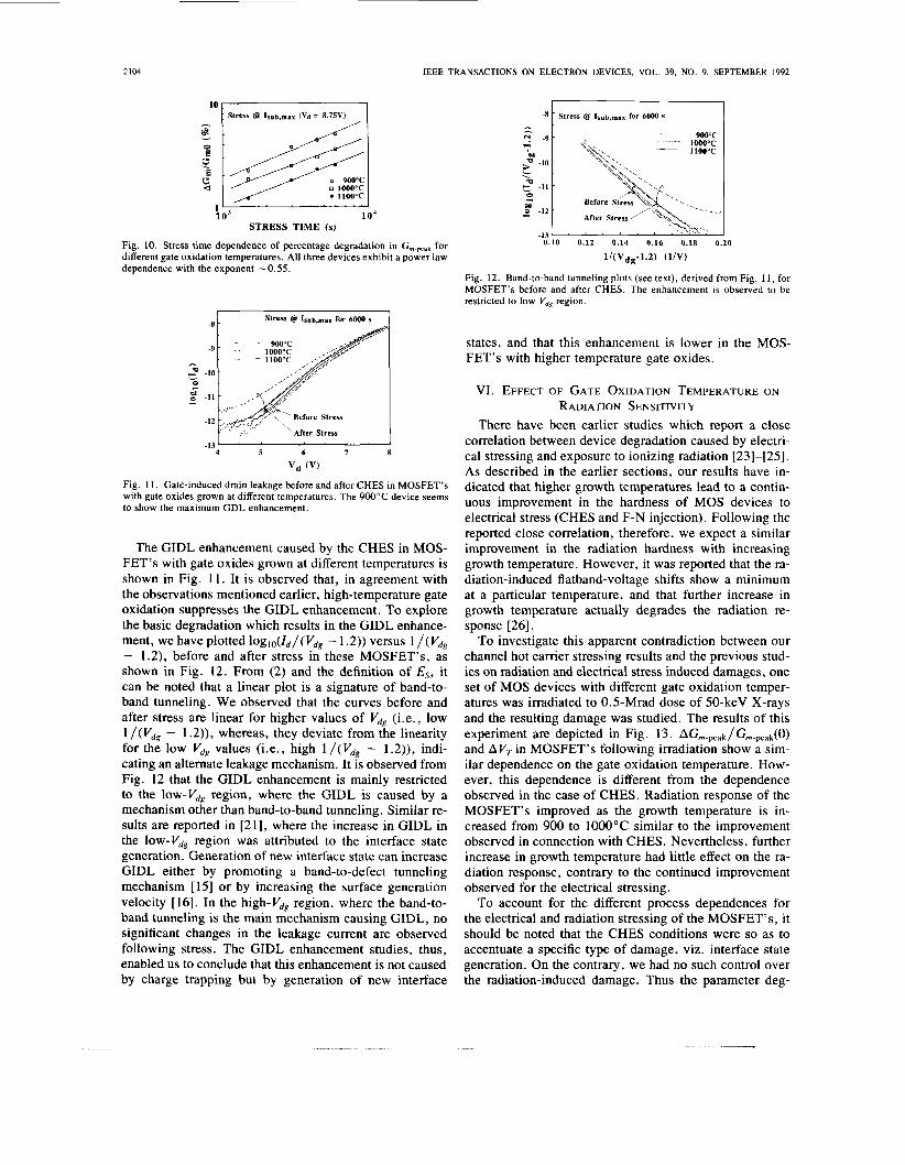
B. Drain Voltage Dependence of GIDL Degradation In an earlier section we indicated a good correlation
between GIDL enhancement in the MOSFET’s and the interface state generation. In this section we utilize a tech- nique based on the GIDL mechanism to corroborate this correlation and also to indicate that the enhancement is suppressed by increasing gate oxide growth temperature.
In order to gain a better insight into our results, a few important points about GIDL are briefly mentioned. GIDL has been indicated to be a result of band-to-band tunnel- ing of electrons under the gate-drain overlap region, which is deep-depleted when zero gate bias and high drain bias are applied [8], [15], [22]. GIDL is modeled by (2), in terms of surface field Es, which can be expressed as E, = (vdg + V’ - 1.2)/3T0, [8]. Here, 1.2 V is the minimum surface band bending necessary to initiate the band-to-band tunneling and 3 is the ratio of dielectric con- stants of Si and SO2.
Id = A * Es * exp ( - B / E s ) . (2) Since the Es is closely related to the charge trapping
through the V’ term, an examination of GIDL before and after the stress can be used to investigation of the cause for GIDL enhancement. We, therefore, studied GIDL as a function of drain bias before and after a channel hot carrier stress performed at peak substrate current condi- tion.
2104 IEEE TRANSACTIONS ON ELECTRON DEVICES, VOL. 39. NO. 9, SEPTEMBER 1992
h .
E ’
2
0 ’ E ,
E , L7 .
10 Stress @ Isub,max (Vd = 8.75V)
1’ i o 3 i o 4
I
STRESS TIME (s)
Fig. 10. Stress time dependence of percentage degradation in Gm~peat for different gate oxidation temperatures. All three devices exhibit a power law dependence with the exponent -0.55.
Stress @ Isub,max fur 6000 s
2 -10 -
. . ~ ~ ~ . h h
1000°C 1100°C
. . .. . ... ..
. U
0
M 0 -12
E -11 - r(
---_., -
U.10 0.12 0.14 0.16 0.18 0.20
1/(V+-1.2) ( l / V )
Fig. 12. Band-to-band tunneling plots (see text), derived from Fig. 11, for MOSFET’s before and after CHES. The enhancement is observed to be restricted to low VdR region.
states, and that this enhancement is lower in the MOS- FET’s with higher temperature gate oxides.
VI. EFFECT OF GATE OXIDATION TEMPERATURE ON RADIATION SENSITIVITY
There have been earlier studies which report a close correlation between device degradation caused by electri- cal stressing and exposure to ionizing radiation [23]-[25]. As described in the earlier sections. our results have in-
Fig. 1 1 . Gate-induced drain leakage before and after CHES in MOSFET’s with gate oxides grown at different temperatures. The 900°C device seems to show the maximum GDL enhancement.
dicated that higher growth temperatures lead to a contin- uous improvement in the hardness of MOS devices to electrical stress (CHES and F-N injection). Following the
The GIDL enhancement caused by the CHES in MOS- FET’s with gate oxides grown at different temperatures is shown in Fig. 11. It is observed that, in agreement with the observations mentioned earlier, high-temperature gate oxidation suppresses the GIDL enhancement. To explore the basic degradation which results in the GIDL enhance- ment, we have plotted logl&/( Vdg - 1.2)) versus 1 /( Vdg - 1.2), before and after stress in these MOSFET’s, as shown in Fig. 12. From (2) and the definition of E,, it can be noted that a linear plot is a signature of band-to- band tunneling. We observed that the curves before and after stress are linear for higher values of Vdg (i.e., low 1 / ( V d g - 1.2)), whereas, they deviate from the linearity for the low Vdg values (i.e., high l/(Vdg - 1.2)), indi- cating an alternate leakage mechanism. It is observed from Fig. 12 that the GIDL enhancement is mainly restricted to the low-Vdg region, where the GIDL is caused by a mechanism other than band-to-band tunneling. Similar re- sults are reported in [21], where the increase in GIDL in the low-vdg region was attributed to the interface state generation. Generation of new interface state can increase GIDL either by promoting a band-to-defect tunneling mechanism [ 151 or by increasing the surface generation velocity [16]. In the high-Vdg region, where the band-to- band tunneling is the main mechanism causing GIDL, no significant changes in the leakage current are observed following stress. The GIDL enhancement studies, thus, enabled us to conclude that this enhancement is not caused by charge trapping but by generation of new interface
reported close correlation, therefore, we expect a similar improvement in the radiation hardness with increasing growth temperature. However, it was reported that the ra- diation-induced flatband-voltage shifts show a minimum at a particular temperature, and that further increase in growth temperature actually degrades the radiation re- sponse [26].
To investigate this apparent contradiction between our channel hot carrier stressing results and the previous stud- ies on radiation and electrical stress induced damages, one set of MOS devices with different gate oxidation temper- atures was irradiated to 0.5-Mrad dose of 50-keV X-rays and the resulting damage was studied. The results of this experiment are depicted in Fig. 13. AGm-peak / Gm-peak(0) and AV, in MOSFET’s following irradiation show a sim- ilar dependence on the gate oxidation temperature. How- ever, this dependence is different from the dependence observed in the case of CHES. Radiation response of the MOSFET’s improved as the growth temperature is in- creased from 900 to 1000°C similar to the improvement observed in connection with CHES. Nevertheless, further increase in growth temperature had little effect on the ra- diation response, contrary to the continued improvement observed for the electrical stressing.
To account for the different process dependences for the electrical and radiation stressing of the MOSFET’s, it should be noted that the CHES conditions were so as to accentuate a specific type of damage, viz. interface state generation. On the contrary, we had no such control over the radiation-induced damage. Thus the parameter deg-
JOSH1 AND KWONG: PERFORMANCE AND RELIABILITY OF THIN MOS GATE OXIDES
-
-
__
2105
0.6
c > 0.5 ?
Dose = 0.5 Mrad (Si021 io” 13.0 [ SO KeV X-rays
10.0 ’ ’ ‘0.4 100 900 1000 1100 1200
TEMPERATURE (“C)
Fig. 13. Percentage degradation of Gm.pcak and AV, following an exposure of MOSFET’s to 50-keV X-rays to a dose of 0.5 Mrad.
radation following irradiation combines the effects of in- terface state generation and fixed charge buildup. A re- cent study [ 101 attempted to isolate the effects of intrinsic and extrinsic defect in irradiated MOSFET’s with gate oxides growth temperatures. The extrinsic defect density caused by irradiation was found to decrease as the growth temperature was increased from 800 to 1000°C [ 101. This is consistent with our results over the 900-1000°C range. Further investigations are necessary to explain the satu- ration of the improvement in radiation response in MOS- FET’s as observed in our work.
VII. QUALITATIVE MODEL In the previous sections, we have observed that the in-
terface state generation is mainly responsible for the deg- radation of on-state (S, G,,,) and off-state ( Id ) . MOSFET parameters, caused by CHES. All our results indicated that the interface state generation is continuously reduced as the oxides are grown at higher temperatures. In this section, we provide a qualitative description of the pro- cesses which may be responsible for the observed effects.
It has been reported that with increasing oxidation tem- perature, there is a reduction in the strain in the oxide film [27]-[29]. This relaxation of strain has been attributed to a viscous flow during oxide growth at elevated tempera- tures which opens up the Si-0-Si bond angle [29] to- wards its magnitude in the bulk oxide. The strain relaxa- tion is associated with a characteristic time (7) which decays with the oxide growth temperature. The net strain in the film depends upon the whether ‘‘7’’ is longer or shorter as compared to the time scale for the oxide growth. Although the time scale for oxide growth reduces with increasing temperature, the decay of “7” with increasing temperature is much faster [29] and, as a result, high- temperature growth results in enhanced strain relaxation. Thus the oxidation process can be described as follows. During the oxidation process, the oxide layer grown at the Si02/Si interface is “pushed” outwards and a new layer is formed at the interface. The outer layer undergoes a viscoelastic relaxation when this new layer is being grown. The higher the growth temperature, the smaller is the characteristic time for strain relaxation, which results in an oxide film with smaller interfacial strain. We have used this model for the strain relaxation in oxides to ex- plain the results of our experiments.
As indicated in [30], depending on the gate polarity during stress in MOS capacitors, two different mechanism are responsible for the interface state generation. Under negative gate bias, as used in our work, the interface state generation was explained by a heated electron impact model. The electrons injected at the gate gain energy from the oxide field. The energy transfer by these electrons to the weak (strained) bonds at the interface results in inter- face state generation. Thus for a particular applied oxide field, density of strained bonds at the interface mainly de- termines the interface state generation. As described ear- lier, high-temperature oxidation leads to fewer strained bonds at the interface and, as a result, interface state gen- eration during F-N injection is suppressed. In addition, less electron trapping, observed in high growth tempera- ture films, leads to smaller anode fields during injection, as compared to the low growth temperature films, thus reducing the electron heating. This further lowers the in- terface state generation.
During CHES of MOSFET’s the scenario is signifi- cantly different from the F-N injection in MOS capaci- tors. First, the normal electrical fields in the oxides are considerably smaller in magnitude than those necessary for F-N injection during substrate injection. Secondly, CHES involves the injection of both electrons and holes into the gate oxide due to the aiding and repelling normal fields along different sections of channel in MOSFET’s during stress. The interface state generation during CHES may be due to a direct bond breaking process at the inter- face by injected electrons which are heated by lateral field in the channel before getting injected into the gate oxide. Thus high density of strained bonds leads to larger density of new interface states. As mentioned in the preceding paragraph, high-temperature oxidation leads to interfacial regions with lower density of strained bonds, thereby ex- hibiting less interface state generation during CHES. Al- ternatively, as modelled by Lai [ 131, interface state gen- eration may result from capture of an electron by a trapped hole. Hole trapping is a precursor for this process. Since high-temperature oxidation leads to a higher density of hole traps as evidenced by the AV, measurements on MOS capacitors, interface state generation by this mechanism is expected to increase with higher growth temperatures, contrary to our observations. To resolve this apparent contradiction, we suggest that holes are captured not only by process-induced hole traps but also by traps generated during the hot electron injection process. Since hole traps are generated by rupture of weak bonds in the Si-0 net- work, higher density of strained bonds leads to more hole trap generation. Since high temperature oxidation, which results in viscoelastic relaxation of the oxide, has fewer strained bonds in the interfacial region, there are fewer hole traps generated during the stress and, therefore, the interface state generation is suppressed.
VIIT. CONCLUSIONS We have examined the effects of gate oxide growth
temperature on the properties of as fabricated MOS ca-
IEEE TRANSACTIONS ON ELECTRON DEVICES, VOL. 39, NO. 9. SEPTEMBER 1992 2 106
pacitors and MOSFET’s and also on the degradation of them under hot carrier stress. Our results indicated that the drive current capability of MOSFET’s is enhanced by oxide growth at higher temperatures. This enhancement was observed to be more prominent for high gate drive and was attributed to high effective mobility due to the formation of a smoother interface at higher temperature.
Less electron trapping and interface state generation was observed in MOS capacitors with high-temperature gate oxides, subjected to constant current stress. High- temperature oxidation was observed to be desirable for less interface state generation under CHES. Degradation of important device parameters such as transconductance and off-state leakage current were found to be correlated with interface state generation. Thus we conclude the high-temperature gate oxidation is desirable to improve the immunity of MOS devices to electrical stress.
Radiation damage in MOSFET’s was also studied as a function of growth temperature. The dependence ob- served was different from that observed for electrical stressing in that, the improvement with increasing growth temperature showed a saturation at 1000°C.
Rapid thermal processing (RTP) utilizes high-temper- ature processing as concluded necessary for a better qual- ity oxide. In addition, it enjoys a reduced thermal budget necessary for a better control over the oxide thickness. These two factors indicate that RTP is a promising tech- nique for the fabrication of high-quality ultrathin gate ox- ides for the future ULSI applications. Alternative ap- proaches such as the use of a weaker oxidizing agent have also been reported recently for the controlled growth of high-quality gate oxides at high temperature [3 11.
ACKNOWLEDGMENT
The authors wish to thank Dr. S. Lee for excellent tech- nical assistance.
REFERENCES
[l] P. 0. Hahn and M. Henzler, “The Si-Si02 interface correlation of atomic structure and electrical properties,” J. Vac. Sri. Technol., vol. A2, no. 2, pp. 574-583, 1984.
[2] J. Nulman, J . Scarpulla, T. Mele, and J. P. Krusius, “Electrical characteristics of thin gate implanted MOS channels grown by rapid thermal processing,” in IEDM Tech. Dig. , 1985, pp. 376-379.
[3] M. Sakashita, S. Zaima, and Y. Yasuda, “Charge trapping and in- terface state generation in metal-oxide-semiconductor capacitors due to Fowler-Nordheim tunneling injection at low temperatures,” J.
[4] E. H. Nicollian and J. R. Brews, MOSPhysics and Technology. New York: Wiley, 1982.
[5] S. C. Sun and J. D. Plummer, “Electron mobility in inversion and accumulation layers on thermally oxidized silicon surface,” IEEE Trans. Electron Devices, vol. ED-27, pp. 1497-1508, 1980.
[6] G. Groesenken, H. E. Maes, N. Beltran, and R. F. De Keersmaecker, “A reliable approach to charge-pumping measurements in MOS tran- sistors,” IEEE Trans. Electron. Devices, vol. ED-3 1, pp. 42-53, 1984.
[7] A. B. Joshi, G. Q. Lo, D. L. Kwong, and S. Lee, “Improved per- formance and reliability of MOSFET’s with thin gate oxides grown at high temperatures,” in Proc. IEEEReliabilify Physics Symp., 1991,
A&. Phys., vol. 67, pp. 6903-6907, 1990.
pp. 316-322.
[8] C. Chang and J . Lien, “Comer-field induced drain leakage current in thin oxide MOSFETs,” in IEDM Tech. Dig . , 1987, pp. 714-717.
[9] C. H. Seager and W. K. Schubert, “Hole trapping in oxides grown by rapid thermal processing,” J. Appl. Phys. , vol. 63, pp. 2869- 2871, 1988.
[ lo] M. Walters and A. Reisman, “The effects of various gate oxidation conditions in intrinsic and radiation-induced extrinsic charged defects and neutral electron traps,” J . Electrochem. Soc., vol. 137, pp. 3596- 3601, 1990.
111 E. P. EerNisse, “Viscous flow of thermal SiO,,” Appl. Phys. Letr.,
121 E. Takeda, N. Suzuki, and T. Hagiwara, “Device performance deg- radation due to hot-camer injection at energies below the Si-SiO, bar- rier,” in IEDM Tech. Dig . , 1983, pp. 396-399.
131 S. K. Lai, “Two-camer nature of interface-state generation in hole trapping and radiation damage,” Appl. Phys. Lett., vol. 39, pp. 58- 60, 1981.
[14] B. Doyle, M. Bourcerie, J. Marchetaux, and A. Boudou, “Interface state creation and charge trapping in the medium-to-high voltage range (Vd/2 t VR t Vd) during hot-camer stressing of n-MOS transis- tors,” IEEE Trans. Electron. Devices, vol. 37, pp. 744-754, 1990.
[15] T. Hori, “Drain-structure design for reduced band-to-band and band- to-defect tunneling leakage,” in Symp. VLSI Tech. Dig . , 1990, pp.
[I61 I. C. Chen, C. W. Teng, D. J. Coleman, and A. Nishimura, “Inter- face-trap enhanced gate-induced leakage current in MOSFET,” IEEE Electron. Device Lett., vol. 10, pp. 216-218, 1989.
[17] E. Takeda, A. Shimuzu, and T. Hagiwara, “Role of hot-hole injec- tion in hot-camer effects and small degraded channel region in MOS- FET’s,” IEEE Electron Device Len., vol. EDL-4, pp. 329-331, 1983.
[18] P. Heremans, H. E. Maes, and N. Saks, “Evaluation of hot camer degradation of n-channel MOSFET’s with the charge pumping tech- nique,” IEEE Electron. Device Letr., vol. EDL-7, pp. 428-430, 1986.
[I91 C. Hu, S. C. Tam, F. C. Hsu, P. K. KO, T . Y. Chan, and K. W. T e d , “Hot-electron-induced MOSFET degradation-model, moni- tor, and improvement,” IEEE Trans. Electron. Devices, vol. ED-32,
[20] E. Takeda and N. Suzuki, “An empirical model for device degrada- tion due to hot-camer injection,” IEEE Electron Device Lett., vol.
[21] G. Q. Lo, A. B. Joshi, and D. L. Kwong, “Hot-camer stress effects on gate-induced drain leakage current in n-channel MOSFET’s,” IEEE Electron Device Lett., vol. 12, pp. 5-7, 1991.
[22] T . Y. Chan, J. Chen, P. K. KO, and C. Hu, “The impact of gate- induced drain leakage current on MOSFET scaling,” in IEDM Tech. Dig. , 1987, pp. 718-721.
[23] Y. Nishioka, E. F. da Silva, Jr., and T. P. Ma, “Equivalence be- tween interface traps in SiO,/Si generated by radiation damage and hot-electron injection,” Appl. Phys. Lett., vol. 52, pp. 720-722, 1988.
[24] J. D. McBrayer, D. M. Fleetwood, R. A. Pastorek, and R. V. Jones, “Correlation of hot-camer and radiation effects in MOS transistors,” IEEE Trans. Nucl. Sr i . , vol. NS-32, pp. 3935-3939, 1985.
[25] L. J . Palkuti, R. D. Ormond, C. Hu, and J. Chung, “Correlation between channel hot-electron degradation and radiation-induced in- terface trapping in MOS devices,” IEEE Trans. Nucl. Sr i . , vol. 36,
[26] G. F . Derbenwick and B. L. Gregory, “Process optimization of ra- diation-hardened CMOS integrated circuits,” IEEE Trans. Nucl. Sri . ,
[27] H. Fukumoto, “Strain measurements of Si at SiO,/Si interface by ion beam channeling,” presented at SSDM-1990, Sendai, Japan.
[28] C. H. Bjorkman, J. T. Fitch, and G. Lucovsky, “Correlation be- tween midgap interface state density and thickness-averaged oxide stress and strain at SiO,/Si interfaces formed by thermal oxidation of Si,” Appl. Phys. Lett., vol. 58, pp. 1983-1985, 1990.
[29] J. T. Fitch, C. H. Bjorkman, J. J. Sumakeris, and G. Lucovsky, “The effects of intrinsic in-plane stress on the local atomic structure of ther- mally grown SiO,,” Mat. Res. Soc. Symp. Proc., vol. 130, pp. 289- 294, 1989.
1301 S. Horiguchi, T. Kobayashi, and T. Sairto, “Interface-trap genera- tion modelling of Fowler-Nordheim tunnel injection into ultra-thin gate oxide,” J. Appl. Phys., vol. 58, pp. 387-391, 1985.
[31] W. Ting, G. Q. Lo, J. Ahn, T . Y. Chu, and D. L. Kwong, “Com- parison of dielectric wear-out between oxides grown in O2 and N,O,” in Proc. IEEE Reliability Physics Symp., 1991, pp. 323-326.
vol. 30, pp. 290-293, 1977.
69-70.
pp. 375-385, 1985.
EDL-4, pp. 111-113, 1983.
pp. 2140-2146, 1989.
vol. NS-22, pp. 2151-2156, 1975.
JOSH1 AND KWONG: PERFORMANCE AND RELIABILITY OF THIN MOS GATE OXIDES 2107
Aniruddha B. Joshi (S’91) was born in India on May 8, 1966. He received the B.Tech. degree in electrical engineering and the M.Tech. degree in microelectronics in 1987 and 1989, respectively, from the Indian Institute of Technology, Bombay.
He is presently working towards the Ph.D. de- gree in solid state electronics in the Microelec- tronics Research Center at the University of Texas at Austin. His current research interests include hot-camer phenomena in submicrometer MOS- FET’s and investieation of Derformance and reli-
Dim-Lee Kwong (A’84-SM’89) was born in Tai- wan, Republic of China, on October 20, 1954. He received the Ph.D. degree in electrical engineer- ing from Rice University, Houston, TX, in 1982.
He is currently a Professor of Electrical and Computer Engineering and the Microelectronics Research Center at The University of Texas at Austin. His primary research interests include rapid thermal processing-CVD technology for the growth and deposition of semiconductor materials compatible with ULSI processes, processing and
ability of alternate gate dielectrics, with a k c u s on &oxidized nitrided ox- ides.
characterization of ultrathin dielectrics for ULSI applicatibns, thin -films and interfaces, Ge,Si,,/Si heterojunctions and optoelectronic devices, light emission from porous Si, hot-camer effects, and diffusion modeling of ion- implanted impurities during RTA. He has published over 250 refereed technical articles and has been granted several patents.