HAL Id: tel-01056404 https://tel.archives-ouvertes.fr/tel-01056404 Submitted on 19 Aug 2014 HAL is a multi-disciplinary open access archive for the deposit and dissemination of sci- entific research documents, whether they are pub- lished or not. The documents may come from teaching and research institutions in France or abroad, or from public or private research centers. L’archive ouverte pluridisciplinaire HAL, est destinée au dépôt et à la diffusion de documents scientifiques de niveau recherche, publiés ou non, émanant des établissements d’enseignement et de recherche français ou étrangers, des laboratoires publics ou privés. Study, optimization and silicon implementation of a smart high-voltage conditioning circuit for electrostatic vibration energy harvesting system Andrii Dudka To cite this version: Andrii Dudka. Study, optimization and silicon implementation of a smart high-voltage conditioning circuit for electrostatic vibration energy harvesting system. Other [cs.OH]. Université Pierre et Marie Curie - Paris VI, 2014. English. NNT: 2014PA066054. tel-01056404
Transcript
HAL Id: tel-01056404https://tel.archives-ouvertes.fr/tel-01056404
Submitted on 19 Aug 2014
HAL is a multi-disciplinary open accessarchive for the deposit and dissemination of sci-entific research documents, whether they are pub-lished or not. The documents may come fromteaching and research institutions in France orabroad, or from public or private research centers.
L’archive ouverte pluridisciplinaire HAL, estdestinée au dépôt et à la diffusion de documentsscientifiques de niveau recherche, publiés ou non,émanant des établissements d’enseignement et derecherche français ou étrangers, des laboratoirespublics ou privés.
Study, optimization and silicon implementation of asmart high-voltage conditioning circuit for electrostatic
vibration energy harvesting systemAndrii Dudka
To cite this version:Andrii Dudka. Study, optimization and silicon implementation of a smart high-voltage conditioningcircuit for electrostatic vibration energy harvesting system. Other [cs.OH]. Université Pierre et MarieCurie - Paris VI, 2014. English. NNT : 2014PA066054. tel-01056404
4 Geometries des transducteurs capacitifs: a) transducteur a rapproche-ment des plans (gap closing), b) transducteur lineaire a mouvement dansle plan (in-plane area overlap), c) transducteur a mouvement dans le planayant une caracteristique Cvar(x) de type dent de scie. . . . . . . . . . . xxiii
5 Trois cycles QV de conversion d’energie par un transducteur capacitif: a)cycle QV a charge constante, b) cycle QV obtenu avec circuit de condi-tionnement primitif c) cycle QV obtenu avec une pompe de charge. . . . . xxiv
6 a) Circuit de conditionnement primitif [Basset09]; b) Circuit de condi-tionnement realisant le cycle QV a charge constante [Meninger01]. . . . . xxvi
8 Evolution de l’etat de la pompe de charge: a) Les tensions Vstore et Vres.Vstore evolue de la tension Vres (5V dans cet exemple) jusqu’a la tensionde saturation (10 V dans cette exemple), Vres ne change presque pas (Cres
est large) b) l’energie convertie par cycle de vibration ∆Wi et depuis ledebut du pompage Wi . . . . . . . . . . . . . . . . . . . . . . . . . . . . . xxviii
9 Pompe de charge avec un circuit de retour resistif. . . . . . . . . . . . . . xxix
10 Circuit de conditionnement a base de la pompe de charge utilisant uncircuit de retour de type convertisseur DC-DC BUCK, propose par Yen[Yen06]. . . . . . . . . . . . . . . . . . . . . . . . . . . . . . . . . . . . . . xxix
11 Evolution de l’etat de la pompe de charge avec circuit de retour: a) Latension Vstore. b) Puissance moyenne de conversion d’energie par cycle devibration ∆Wi. . . . . . . . . . . . . . . . . . . . . . . . . . . . . . . . . xxx
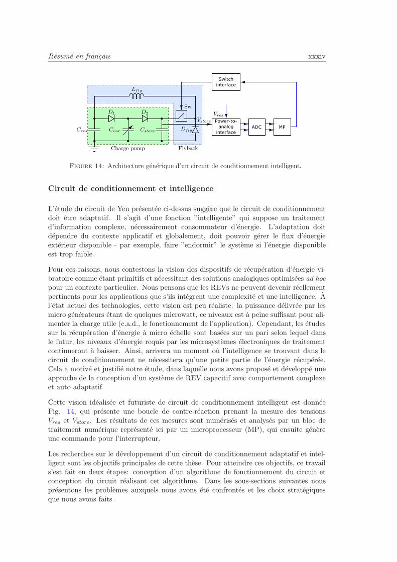
14 Architecture generique d’un circuit de conditionnement intelligent. . . . . xxxiv
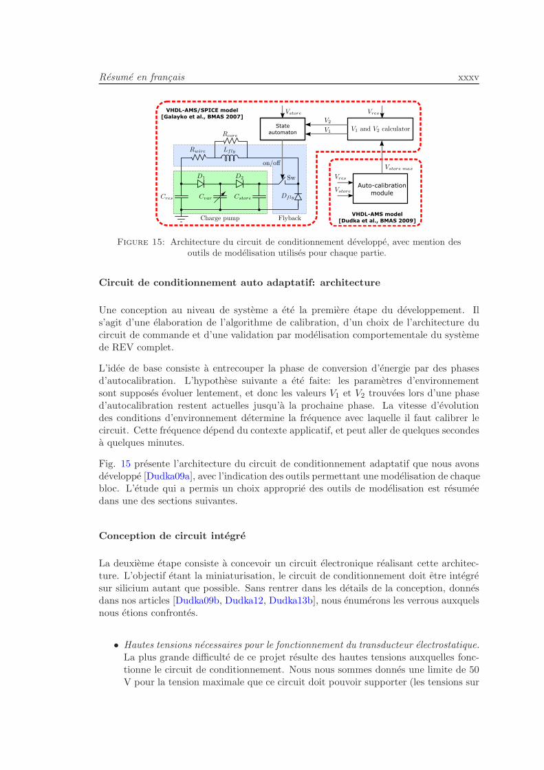
15 Architecture du circuit de conditionnement developpe, avec mention desoutils de modelisation utilises pour chaque partie. . . . . . . . . . . . . . xxxv
16 Illustration du probleme de la commande d’un interrupteur ”flottant”haute tension. . . . . . . . . . . . . . . . . . . . . . . . . . . . . . . . . . xxxvi
vii
List of Figures viii
17 Circuit de commande de l’interrupteur avec un nouveau elevateur de ten-sion, circuit realise en technologie AMS035HV [Dudka12]: (a) schema (b)layout. . . . . . . . . . . . . . . . . . . . . . . . . . . . . . . . . . . . . . . xxxvi
20 Evolution de l’etat du systeme etudie en mode autonome soumis a desvibrations externes stochastiques avec trois stimuli differents. En haut :tension aux bornes de Cres = 1µF, en bas : energie de Cres. . . . . . . . . xliii
2.1 Block diagram of an electrostatic vibration energy harvester assisted bya ’charge pump and flyback’ conditioning circuit [Yen06]. . . . . . . . . . . 28
2.2 Schema of the VEH system employing the auto-synchronous conditioningcircuit with an inductive flyback return, proposed by Yen and Lang [Yen06]. 29
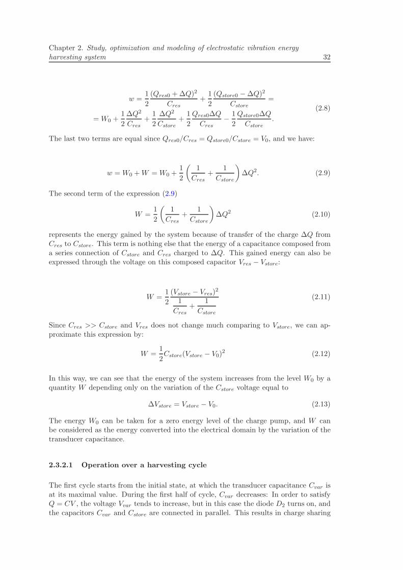
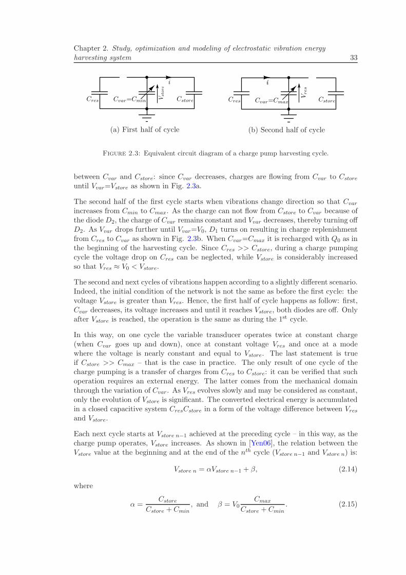
2.3 Equivalent circuit diagram of a charge pump harvesting cycle. . . . . . . . 33
2.4 Example of the evolution of the charge pump state during numerous nCvar variation cycles: (a) voltages Vres and Vstore: Vstore rises from V0=5V up to the saturation (e.g. 10 V); (b) instantaneous energy harvested ata vibration cycle ∆Wi and total energy accumulated from the beginningof the charge pumping Wi. . . . . . . . . . . . . . . . . . . . . . . . . . . . 34
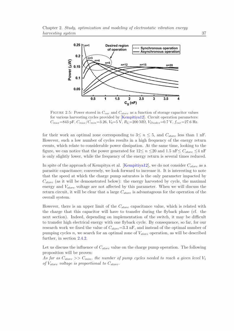
2.5 Power stored in Cvar and Cstore as a function of storage capacitor valuesfor various harvesting cycles provided by [Kempitiya12]. Circuit opera-tion parameters: Cmax=843 pF, Cmax/Cmin=3.26, V0=5 V, RL=200 MΩ,VDiodes=0.7 V, fvar=27.6 Hz. . . . . . . . . . . . . . . . . . . . . . . . . . 37
List of Figures ix
2.6 QV-diagram corresponding to energy conversion by capacitive transducerfor each charge pump cycle. . . . . . . . . . . . . . . . . . . . . . . . . . . 39
2.7 Equivalent flyback circuit diagram of energizing (a) and de-energizing(b) the inductor; (c) illustration of the flyback operation: current in theflyback path and voltage Vstore. . . . . . . . . . . . . . . . . . . . . . . . . 43
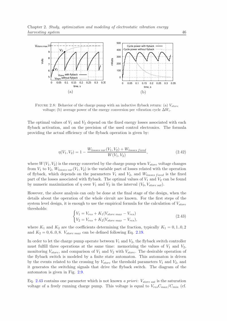
2.8 Behavior of the charge pump with an inductive flyback return: (a) Vstore
voltage; (b) average power of the energy conversion per vibration cycle∆Wi. . . . . . . . . . . . . . . . . . . . . . . . . . . . . . . . . . . . . . . . 46
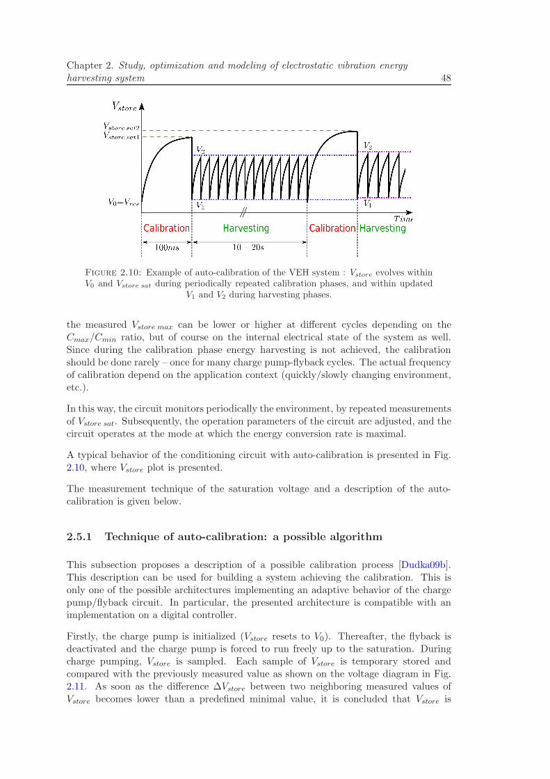
2.10 Example of auto-calibration of the VEH system : Vstore evolves within V0
and Vstore sat during periodically repeated calibration phases, and withinupdated V1 and V2 during harvesting phases. . . . . . . . . . . . . . . . . 48
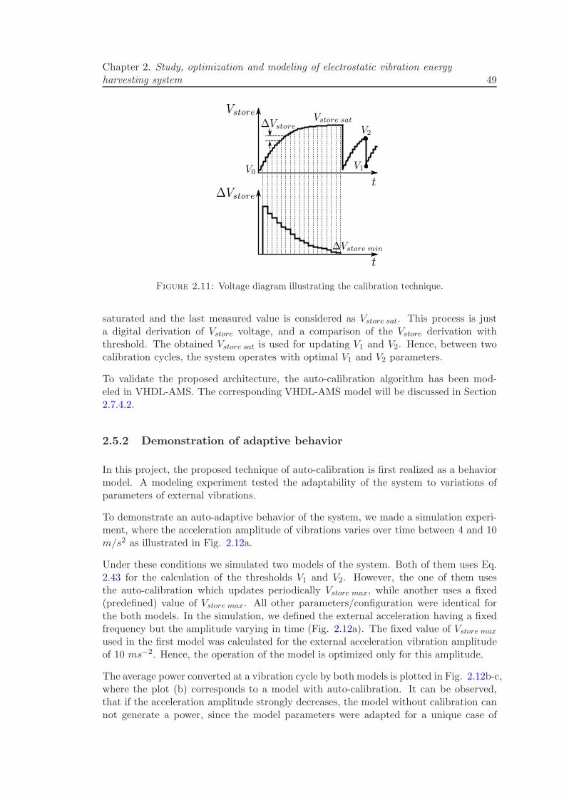
2.11 Voltage diagram illustrating the calibration technique. . . . . . . . . . . . 49
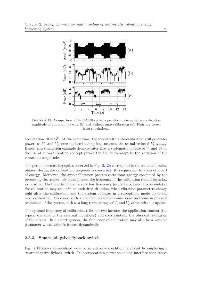
2.12 Comparison of the E-VEH system operation under variable accelerationamplitude of vibration (a) with (b) and without auto-calibration (c).Plots are issued from simulations. . . . . . . . . . . . . . . . . . . . . . . . 50
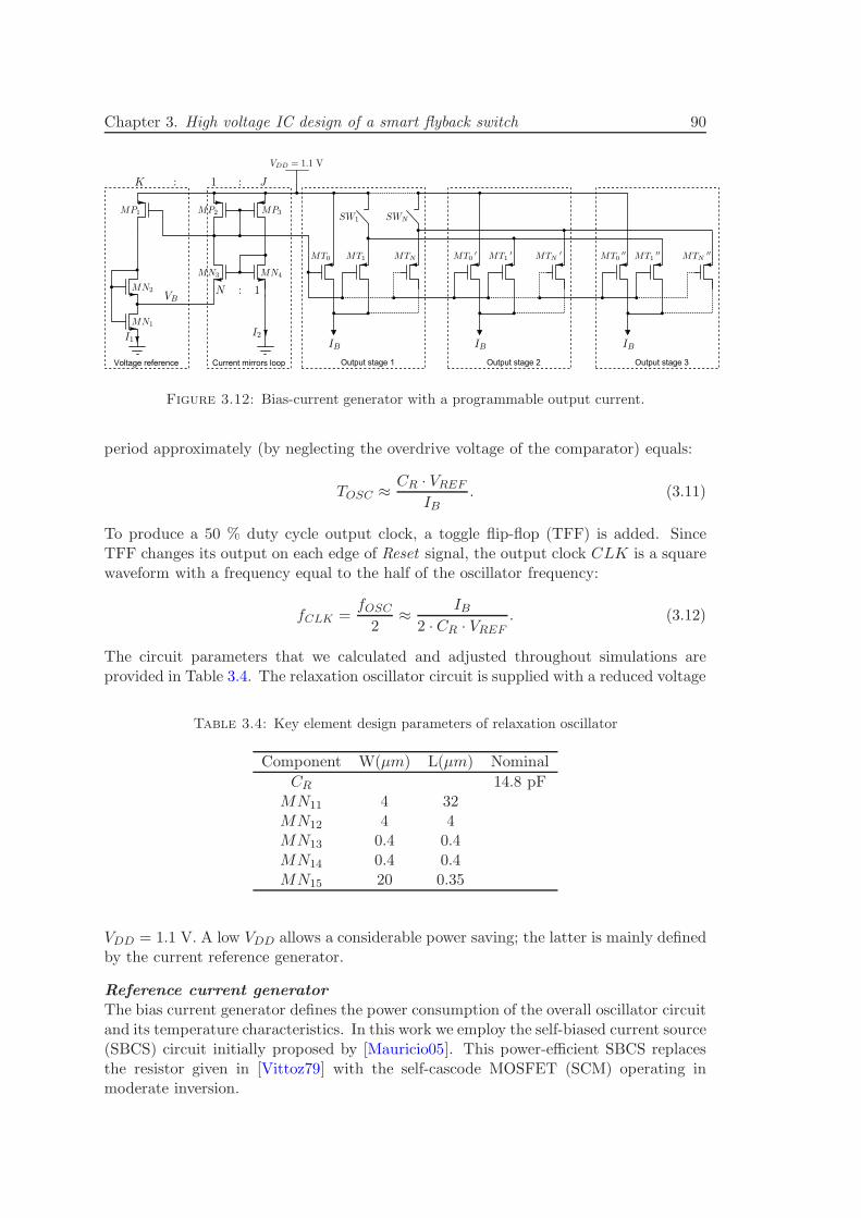
3.12 Bias-current generator with a programmable output current. . . . . . . . 90
3.13 AMS035HV layout of a programmable frequency relaxation oscillator . . . 93
3.14 Synchronous voltage divider with low current consumption . . . . . . . . 94
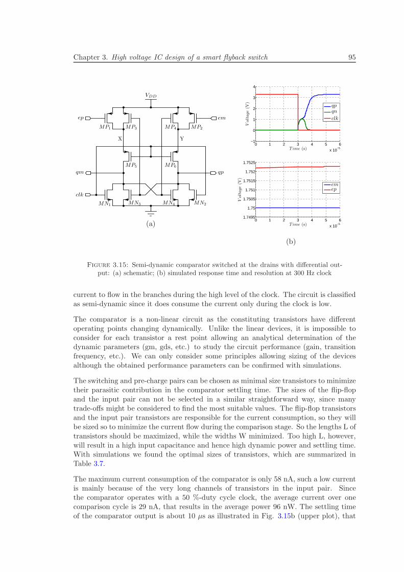
3.15 Semi-dynamic comparator switched at the drains with differential output:(a) schematic; (b) simulated response time and resolution at 300 Hz clock 95
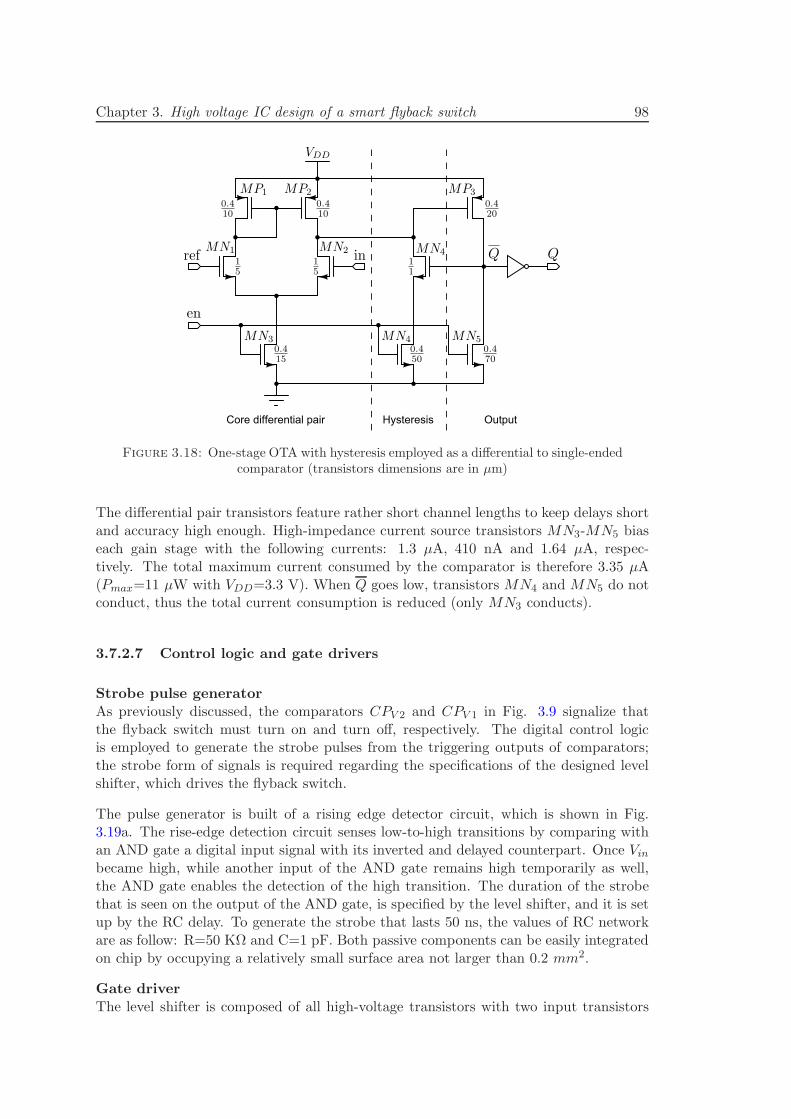
3.18 One-stage OTA with hysteresis employed as a differential to single-endedcomparator (transistors dimensions are in µm) . . . . . . . . . . . . . . . 98
3.19 (a) Digital rise-edge detection circuit for strobe generation; (b) Gatedriver (transistors dimensions are in µm). . . . . . . . . . . . . . . . . . . 99
3.20 Simulation results of the proposed VEH IC: (a) Harvester long-term op-eration; (b) Zoom on the calibration phase; (c) Zoom on the flyback phase.100
3.21 Contribution to the average power (per 50 seconds) by the conditioningcircuit and the proposed adaptive switch controller. Parameters of sim-ulation example: Vres=10→15 V, Cmax/Cmin=1.6, fext=298 Hz, Aext=1g. . . . . . . . . . . . . . . . . . . . . . . . . . . . . . . . . . . . . . . . . . 102
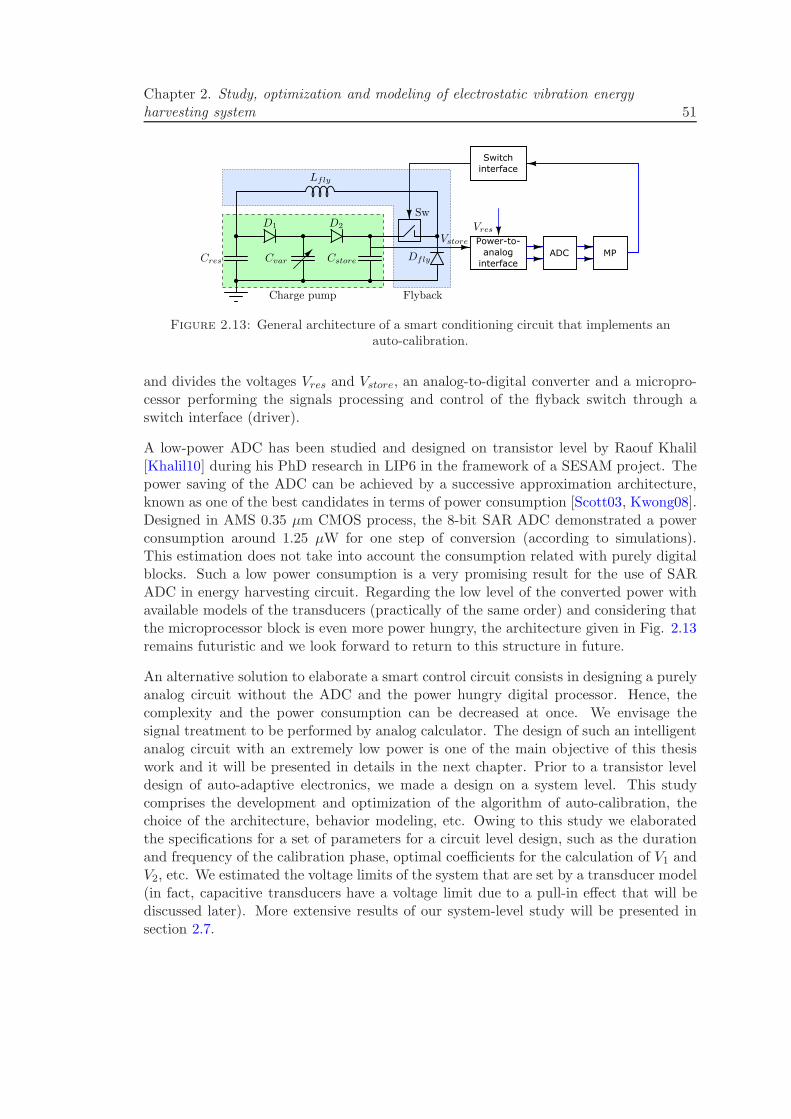
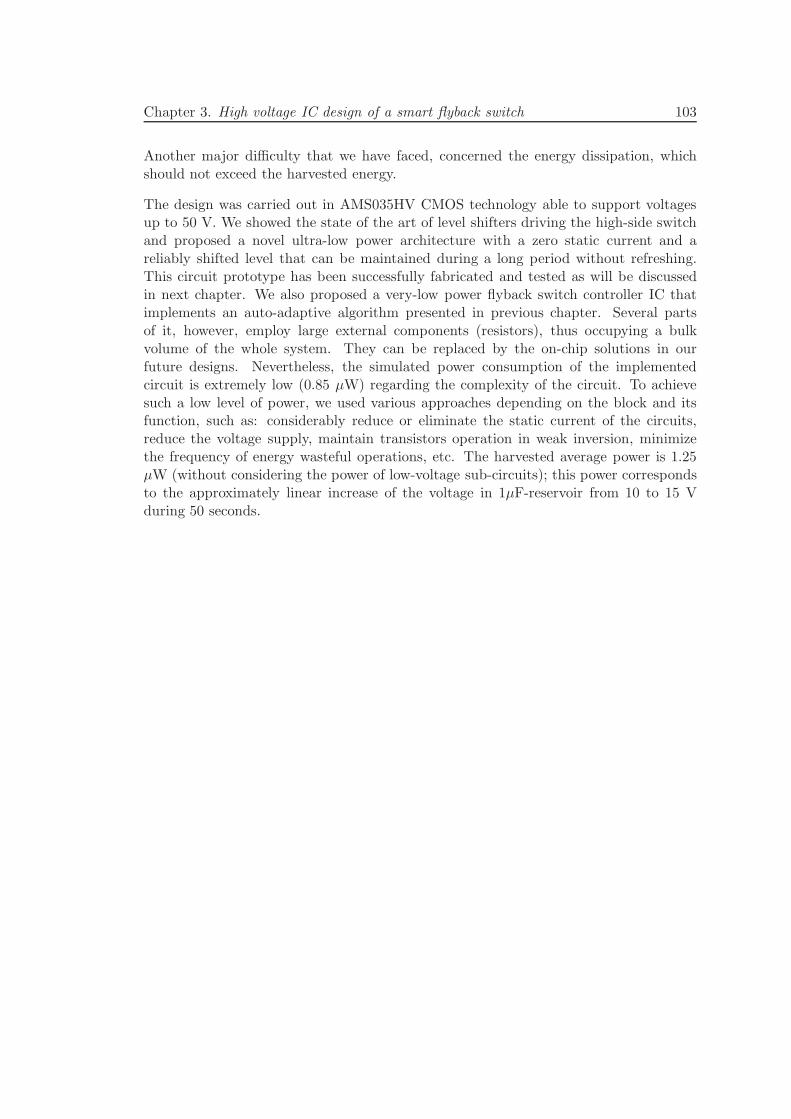
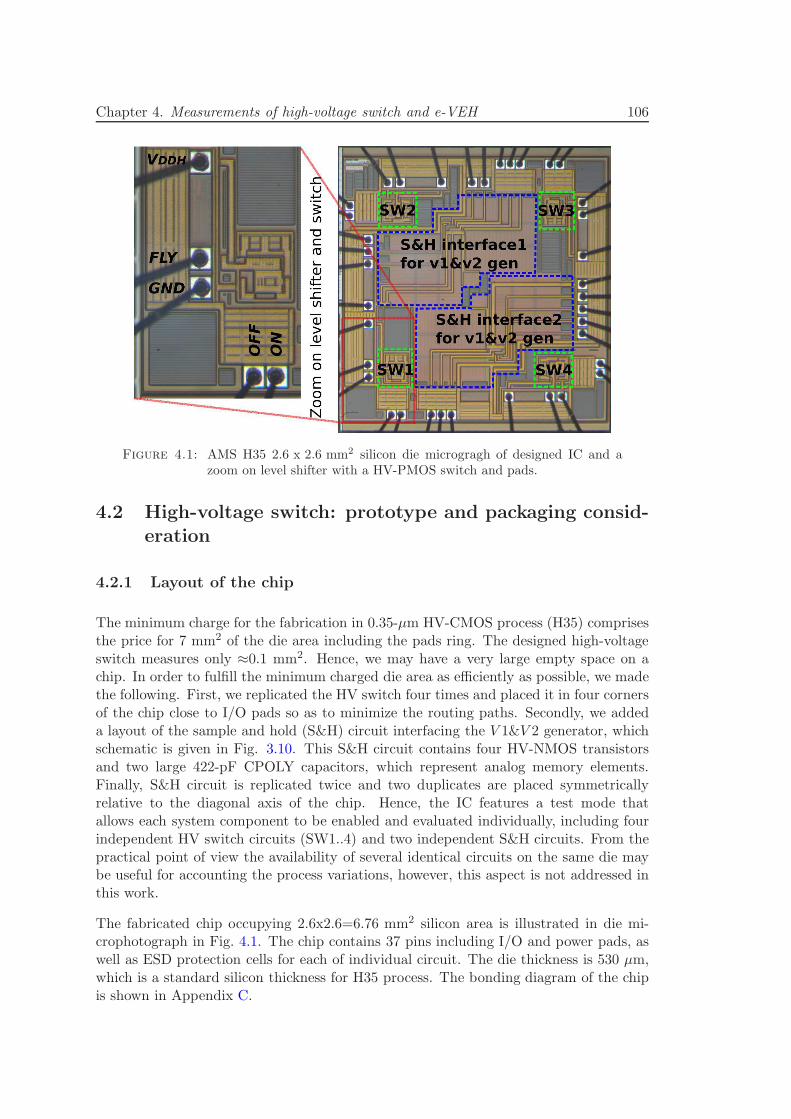
4.1 AMS H35 2.6 x 2.6 mm2 silicon die microgragh of designed IC and a zoomon level shifter with a HV-PMOS switch and pads. . . . . . . . . . . . . . 106
4.12 Experimental setups for measuring the leakage current of the HV switch:(a) measurement of CMeas leakage current via the input of OPAMP; (b)measurement of CMeas leakage current via the input of OPAMP and viathe measuring IC pin; . . . . . . . . . . . . . . . . . . . . . . . . . . . . . 115
4.13 Illustration of principle of the experiment. Discharge buffered voltagesVMeasBUF slopes for two experiments (i.e., with and without LS) . . . . . 116
4.14 a) Leakage current of LS; Static power consumption of LS. . . . . . . . . . 117
4.15 External amplifiers buffering VFLY for measurement of duration of on-state of the level shifter . . . . . . . . . . . . . . . . . . . . . . . . . . . . 118
4.16 Experimental measurements showing the maximum time that LS can holdthe ON-state, where the switch is close. . . . . . . . . . . . . . . . . . . . 118
4.18 Minimum VDDH voltage that can be applied to level shifter with respectto the control voltage level of VON and VOFF . . . . . . . . . . . . . . . . 120
4.20 Picture of the MEMS electrostatic energy harvester harvester [Guillemet13]122
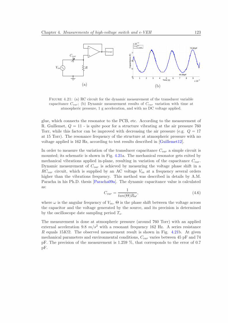
4.21 (a) RC circuit for the dynamic measurement of the transducer variablecapacitance Cvar; (b) Dynamic measurement results of Cvar variation withtime at atmospheric pressure, 1 g acceleration, and with no DC voltageapplied. . . . . . . . . . . . . . . . . . . . . . . . . . . . . . . . . . . . . . 123
4.22 Picture of the measurement setup, illustrating the conditioning circuitand the control logic mounted on the breadboard and the . . . . . . . . . 124
4.23 Schematic of the setup for characterization of both, MEMS-device andintegrated flyback switch, in context of the [Yen06] conditioning circuit . . 125
4.24 Evolution of measured voltages Vres and Vstore and of accumulated energyin reservoir capacitor, as the harvester oscillates at the frequency 170 Hzwith the acceleration amplitude 1.5 g . . . . . . . . . . . . . . . . . . . . . 127
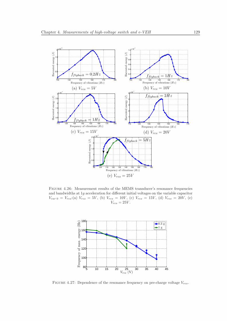
4.27 Dependence of the resonance frequency on pre-charge voltage Vres. . . . . 129
List of Figures xii
4.28 Evolution of Vres and Vstore as the e-VEH is submitted to mechanicalvibrations with 150Hz@1g with a flyback frequency ffb=1Hz. . . . . . . . 130
4.29 Evolution of Vres and Vstore as the e-VEH is submitted to mechanicalvibrations with 150Hz@1g with a flyback frequency ffb=5Hz. . . . . . . . 130
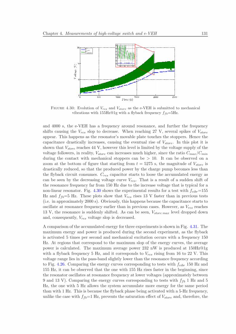
4.30 Evolution of Vres and Vstore as the e-VEH is submitted to mechanicalvibrations with 155Hz@1g with a flyback frequency ffb=5Hz. . . . . . . . 131
4.31 Evolution of energy corresponding to 3 similar experiments with followingsetup parameters: (a) fvibr=150 Hz and ffb=1 Hz, (b) fvibr=150 Hz andffb=5 Hz, (c) fvibr=155 Hz and ffb=5 Hz. Acceleration amplitude for alltests is 1 g. . . . . . . . . . . . . . . . . . . . . . . . . . . . . . . . . . . . 132
4.32 Exponentially correlated Gaussian noise signal of a 1-second durationcomprising frequencies in 100 − 180 Hz bandwidth. . . . . . . . . . . . . . 132
4.33 Evolution of Vres and Wres curves as the e-VEH is exposed to mechanicalvibrations occurring in a form of exponentially correlated Gaussian noise. 133
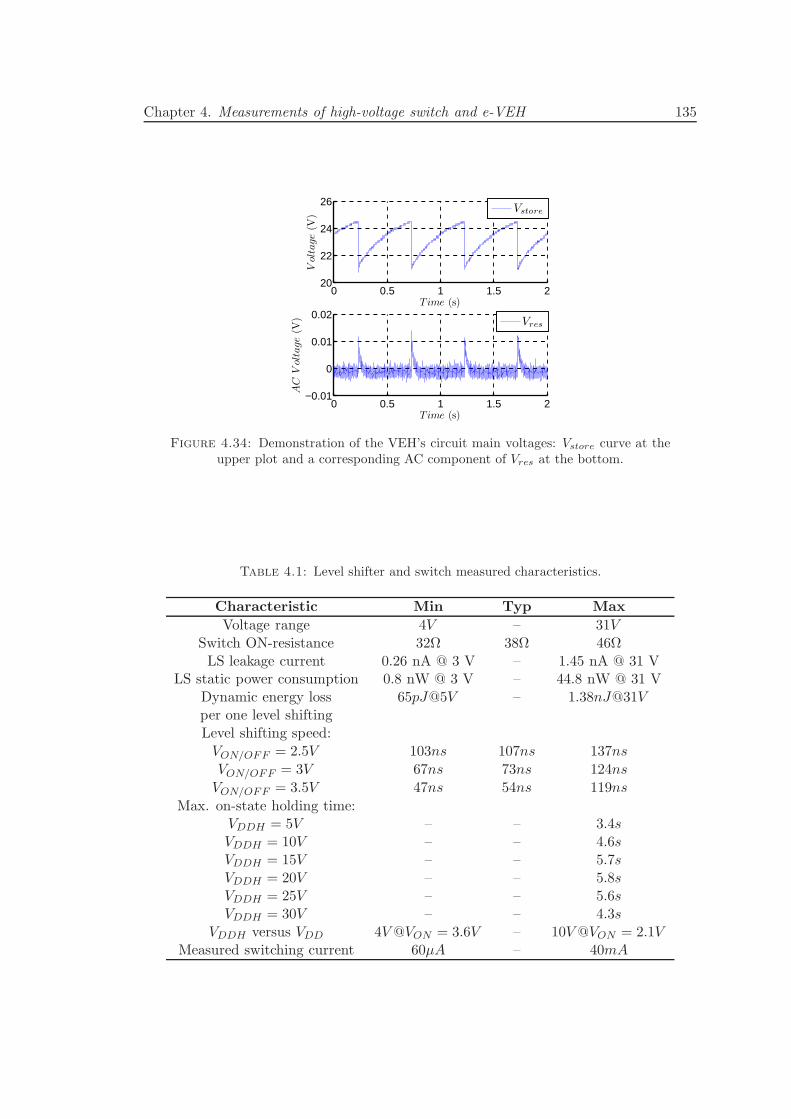
4.34 Demonstration of the VEH’s circuit main voltages: Vstore curve at theupper plot and a corresponding AC component of Vres at the bottom. . . 135
List of Tables
3 Les caracteristiques principales de l’elevateur de tension et de l’interrupteurfabriques : mesures versus simulation. . . . . . . . . . . . . . . . . . . . . xli
1.1 A comparison of energy sources according to [Rabaey00, Roundy03a,Stordeur97, Vullers09, Zelenay04] . . . . . . . . . . . . . . . . . . . . . . . 5
1.2 Summary of several vibrations sources accordingly to [Roundy03b] . . . . 8
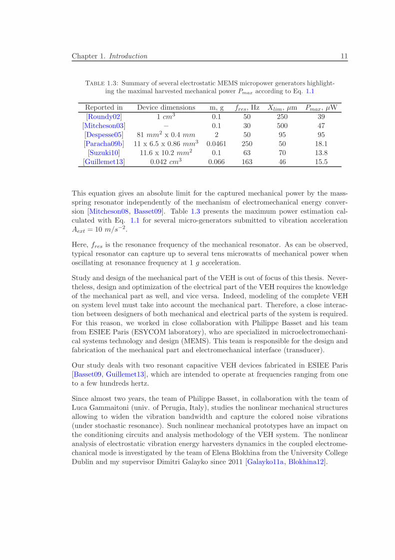
1.3 Summary of several electrostatic MEMS micropower generators highlight-ing the maximal harvested mechanical power Pmax according to Eq. 1.1 . 11
1.4 Comparison characteristics of vibration energy harvesting techniques -electromagnetic (EM), electrostatic (ES) and piezoelectric (PE). . . . . . 13
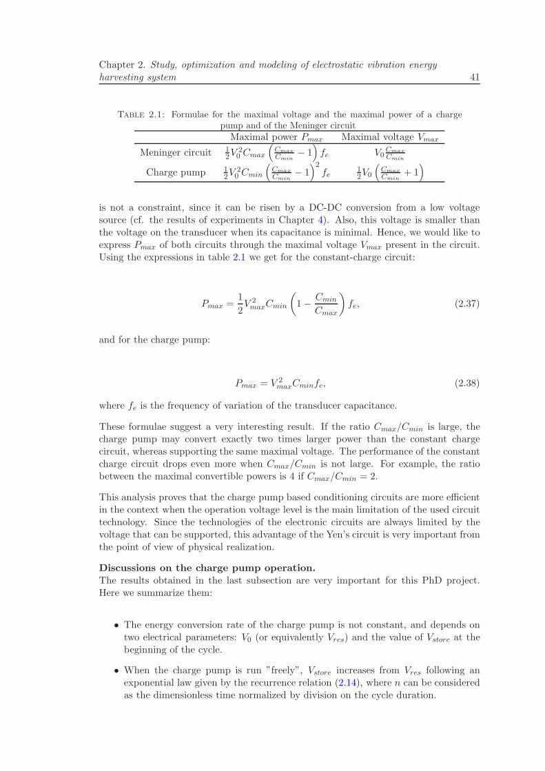
2.1 Formulae for the maximal voltage and the maximal power of a chargepump and of the Meninger circuit . . . . . . . . . . . . . . . . . . . . . . 41
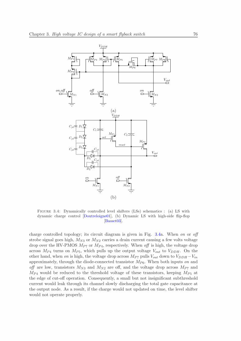
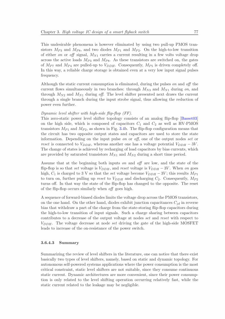
3.3 Comparison of the efficiency of the flyback circuit that comprises theconventional and improved level shifters driving the switch . . . . . . . . . 84
3.4 Key element design parameters of relaxation oscillator . . . . . . . . . . . 90
E-VEH Electrostatic Vibration Energy HarvesterRF Radio FrequencyWSN Wireless Sensor NodeMEMS Microelectromechanical SystemPZT Lead zirconate titanate (piezoelectric material)ICP Integrated Circuit PiezoelectricDRIE Deep Reactive-Ion EtchingOPGP Out-of-Plane Gap-closing PlateIPOP In-Plane Overlap PlatesIPOC In-Plane Overlap CombIPGC In-Plane Gap-closing CombSESAM Smart multi-source Energy Scavenger for Autonomous MicrosystemsCC Conditioning CircuitEM Electro-MagneticSAR ADC Successive Approximation Register Analog-to-Digital ConverterAMS Austria Microsystems and Analog Mixed SignalsMP MicroprocessorCAD Computer-Aided DesignASIC Application-Specific Integrated CircuitESD Electrostatic-DischargeLS Level-ShifterDCC Dynamic Charge ControlPTAT Proportional-To-Absolute TemperatureSBCS Self-Biased Current SourceSCM Self-Cascode MOSFETACM Advanced-Compact MOSFETMIM Metal-Insulator-MetalPIP Poly-Insulator-PolyJLCC J-Leaded Chip CarrierESR Equivalent Series ResistanceRMS Root Mean Square
xv
Symbols
Symbol Name Unit
I current AV voltage VW energy Jt time sP power WAext acceleration of external vibrations ms−1
Xlim displacement limit mA overlap area of the plates m2
d gap distance between the plates mQ electrical charge CC capacitance FL inductance HR resistance Ωf frequency HzT period sm mass gk stiffness Nm−1
Tabs absolute temperature K
ω angular frequency rads−1
ε0 dielectric constantτ time constant sη efficiencyµ damping coefficient Nsm−1
φ thermal voltage VκB the Boltzmann constant JK−1
µe electron mobility m2(Vs)−1
xvii
Resume en francais
Cette these resume nos travaux de recherche sur la recuperation d’energie vibratoire(REV) pour l’alimentation des systemes embarques/implante autonomes ultra-basseconsommation. Ces travaux ont ete possible grace a un projet de recherche ANRSESAM1, dont l’objectif etait le developpement d’un microsysteme de recuperation et demanagement de l’energie ambiante (vibratoire, solaire et thermique), adaptable, recon-figurable et robuste. Le projet regroupe 4 partenaires (responsabilites): le LIP6 (partieelectronique pour le REV capacitive), l’ESIEE (convertisseur REV capacitive), le TIMA(convertisseur REV piezoelectrique) et le CEA-LETI (partie management de l’energieconvertie et les convertisseurs solaires et thermique). Notre recherche sur la partieelectronique du REV a base d’un convertisseur capacitive se porte sur l’etude theorique,la modelisation et la conception d’un circuit intelligent adaptative et autonome.
Le manuscrit presente des generalites sur les systemes de recuperation d’energie vibra-toire en resumant nos contributions, expose le probleme de conditionnement des trans-ducteurs capacitifs, presente le travail de conception et de modelisation des circuits deconditionnement integres et, finalement, expose la partie experimentale des prototypesfabriques (une puce electronique a LIP6 et un dispositif MEMS a l’ESIEE Paris).
Introduction: systeme de recuperation d’energie vibratoire
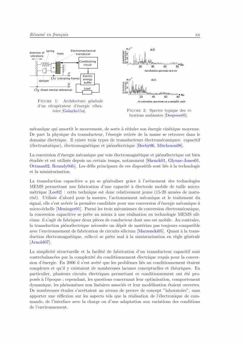
Fig. 1 presente un schema general d’un systeme de recuperation d’energie vibratoire.Deux elements font toujours partie d’un recuperateur d’energie vibratoire (REV) : unemasse mobile (masse sismique) dont le role est d’emmagasiner une partie d’energie del’environnement et un transducteur electromecanique realisant une interface physiqueentre le domaine mecanique et le domaine electrique. La masse mobile est coupleepar un ressort avec le systeme exterieur vibrant. La conception d’un REV consiste aoptimiser la partie mecanique et la partie liee au transducteur de sorte a ce que l’ensembleconvertisse le plus d’energie possible.
Transduction electromecanique et son conditionnement
Le role du transducteur est la conversion d’energie du domaine mecanique vers le do-maine electrique. Pour cela, le transducteur genere sur la masse mobile une force
1Smart multi-source Energy Scavenger for Autonomous Microsystems
toire [Galayko11a]. Figure 2: Spectre typique des vi-brations ambiantes [Despesse05].
mecanique qui amortit le mouvement, de sorte a reduire son energie cinetique moyenne.De part la physique du transducteur, l’energie retiree de la masse se retrouve dans ledomaine electrique. Il existe trois types de transducteurs electromecaniques: capacitif(electrostatique), electromagnetique et piezoelectrique [Beeby06, Mitcheson08].
La conversion d’energie mecanique par voie electromagnetique et piezoelectrique est bienetudiee et est utilisee depuis un certain temps, notamment [Shenck01, Glynne-Jones01,Ottman02, Roundy04b]. Les defis principaux de ces dispositifs sont lies a la technologieet la miniaturisation.
La transduction capacitive a pu se generaliser grace a l’avenement des technologiesMEMS permettant une fabrication d’une capacite a electrode mobile de taille micro-metrique [Lee82] : cette technique est donc relativement jeune (15-20 annees de matu-rite). Utilisee d’abord pour la mesure, l’actionnement mecanique et le traitement dusignal, elle s’est averee la premiere candidate pour une conversion d’energie mecanique amicro-echelle [Meninger01]. Parmi les trois mecanismes de conversion electromecanique,la conversion capacitive se prete au mieux a une realisation en technologie MEMS sili-cium: il s’agit de fabriquer deux pieces de conducteur dont une est mobile. Au contraire,la transduction piezoelectrique necessite un depot de materiau pas toujours compatibleavec l’environnement de fabrication de circuits silicium [Marzencki05]. Quant a la trans-duction electromagnetique, celle-ci se prete mal a la miniaturisation en regle generale[Arnold07].
La simplicite structurelle et la facilite de fabrication d’un transducteur capacitif sontcontrebalancees par la complexite du conditionnement electrique requis pour la conver-sion d’energie. En 2006 il s’est avere que les problemes lies au conditionnement etaientcomplexes et qu’il y existaient de nombreuses lacunes conceptuelles et theoriques. Enparticulier, plusieurs circuits electriques permettant ce conditionnement ont ete pro-poses a l’epoque ; cependant, les questions concernant leur optimisation, comportementdynamique, les phenomenes non lineaires associes et leur modelisation etaient ouvertes.De nombreuses etudes s’arretaient au niveau de preuve de concept ”laboratoire”, sansapporter une reflexion sur les aspects tels que la realisation de l’electronique de com-mande, de l’interface avec la charge ou d’une adaptation aux variations des conditionsde l’environnement.
Resume en francais xxi
Partie mecanique
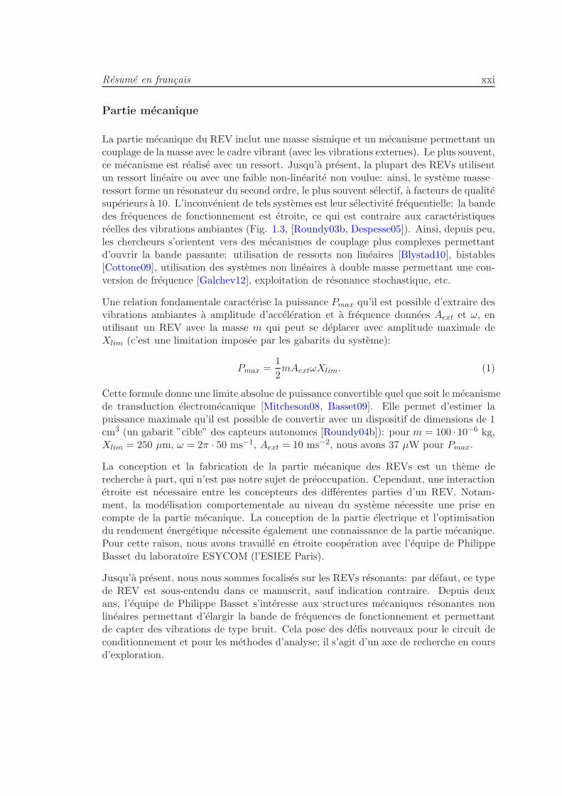
La partie mecanique du REV inclut une masse sismique et un mecanisme permettant uncouplage de la masse avec le cadre vibrant (avec les vibrations externes). Le plus souvent,ce mecanisme est realise avec un ressort. Jusqu’a present, la plupart des REVs utilisentun ressort lineaire ou avec une faible non-linearite non voulue: ainsi, le systeme masse–ressort forme un resonateur du second ordre, le plus souvent selectif, a facteurs de qualitesuperieurs a 10. L’inconvenient de tels systemes est leur selectivite frequentielle: la bandedes frequences de fonctionnement est etroite, ce qui est contraire aux caracteristiquesreelles des vibrations ambiantes (Fig. 1.3, [Roundy03b, Despesse05]). Ainsi, depuis peu,les chercheurs s’orientent vers des mecanismes de couplage plus complexes permettantd’ouvrir la bande passante: utilisation de ressorts non lineaires [Blystad10], bistables[Cottone09], utilisation des systemes non lineaires a double masse permettant une con-version de frequence [Galchev12], exploitation de resonance stochastique, etc.
Une relation fondamentale caracterise la puissance Pmax qu’il est possible d’extraire desvibrations ambiantes a amplitude d’acceleration et a frequence donnees Aext et ω, enutilisant un REV avec la masse m qui peut se deplacer avec amplitude maximale deXlim (c’est une limitation imposee par les gabarits du systeme):
Pmax =1
2mAextωXlim. (1)
Cette formule donne une limite absolue de puissance convertible quel que soit le mecanismede transduction electromecanique [Mitcheson08, Basset09]. Elle permet d’estimer lapuissance maximale qu’il est possible de convertir avec un dispositif de dimensions de 1cm3 (un gabarit ”cible” des capteurs autonomes [Roundy04b]): pour m = 100 · 10−6 kg,Xlim = 250 µm, ω = 2π · 50 ms−1, Aext = 10 ms−2, nous avons 37 µW pour Pmax.
La conception et la fabrication de la partie mecanique des REVs est un theme derecherche a part, qui n’est pas notre sujet de preoccupation. Cependant, une interactionetroite est necessaire entre les concepteurs des differentes parties d’un REV. Notam-ment, la modelisation comportementale au niveau du systeme necessite une prise encompte de la partie mecanique. La conception de la partie electrique et l’optimisationdu rendement energetique necessite egalement une connaissance de la partie mecanique.Pour cette raison, nous avons travaille en etroite cooperation avec l’equipe de PhilippeBasset du laboratoire ESYCOM (l’ESIEE Paris).
Jusqu’a present, nous nous sommes focalises sur les REVs resonants: par defaut, ce typede REV est sous-entendu dans ce manuscrit, sauf indication contraire. Depuis deuxans, l’equipe de Philippe Basset s’interesse aux structures mecaniques resonantes nonlineaires permettant d’elargir la bande de frequences de fonctionnement et permettantde capter des vibrations de type bruit. Cela pose des defis nouveaux pour le circuit deconditionnement et pour les methodes d’analyse; il s’agit d’un axe de recherche en coursd’exploration.
Resume en francais xxii
Resume de notre contribution
Notre contribution au theme de la recuperation d’energie est structuree autours despoints suivants:
– Etude globale du systeme de REV: analyse et optimisation. Un REV est unsysteme fonctionnant dans deux domaines physiques fortement couples. Son optimisa-tion necessite une approche globale, prenant en compte a la fois la partie mecanique, latransduction et la partie electrique. La plupart des etudes precedentes sont focaliseessur un de ces aspects. Dans nos publications, nous avons defendu la vision selon laquelleun transducteur electromecanique doit etre considere en un bloc uni avec son circuit deconditionnement; l’etude d’un REV se reduit alors a analyser l’interaction entre ce blocet le resonateur mecanique.
– Techniques de modelisation multiphysique a differents niveaux de raffine-ment. L’objectif d’une demarche de modelisation est de pouvoir etudier le comporte-ment d’un systeme dont les phenomenes sont trop complexes pour etre decrits analy-tiquement. La modelisation est egalement un precieux outil de conception. Elle permetune approche de conception ”top-down”. Selon cette approche, la conception se faitd’abord au niveaux de blocs representes par leurs macromodeles comportementaux. En-suite, chaque bloc est detaille au fur et a mesure. Une modelisation a differents niveauxde raffinement permet de melanger les niveaux d’abstraction dans une meme simulation: un bloc represente par un modele structurel tres precis (par ex., une netlist SPICE ex-trait d’un dessin de masques d’un circuit integre) et des blocs representes par des modelesde haut niveau d’abstraction (par ex., un modele VHDL-AMS d’un resonateur).
– Circuits de conditionnement integres: analyse et conception La conceptionde l’electronique de conditionnement pour transducteurs capacitifs represente le plusgrand defi parmi ceux poses par les REVs. Comme il sera presente, un circuit de con-ditionnement doit ordonner des interrupteurs selon un protocole precis permettant uneconversion d’energie en mode optimal. La situation est compliquee par deux contraintesqui s’opposent. Une haute tension est necessaire pour le fonctionnement des transduc-teurs capacitifs, en meme temps, le circuit doit etre ultra basse consommation (des mi-crowatts). Nous avons etudie plusieurs circuits de conditionnement, et par la suite nousavons propose une nouvelle architecture basee sur une pompe de charge, qui s’adapteaux conditions reelles de l’environnement. Ce circuit est concu dans une technologiede circuits integres CMOS haute tension et represente une contribution significative audomaine des circuits integres de puissance.
REV capacitifs: presentation globale et problemes associes
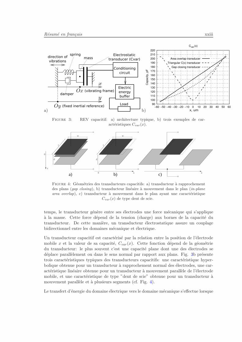
Description d’un REV capacitif
Un schema general de REV capacitif est identique a celui presente Fig. 1, avec, a la placedu transducteur generique, un condensateur a une electrode mobile (Fig. 3a). La massemobile du resonateur est associee a l’electrode mobile du transducteur capacitif, ce quifait que la capacite du transducteur varie avec le mouvement de la masse. En meme
Resume en francais xxiii
a)
Load
Electric
energy
buffer
Conditioning
circuit
Electrostatic
transducer (Cvar)massspring
direction of
vibrations
(vibrating frame)
(fixed inertial reference)
damper
b)
90
100
110
120
130
140
150
160
170
180
190
200
210
220
−60 −50 −40 −30 −20 −10 0 10 20 30 40 50 60
Capacity, pF
Cvar (x)
Area overlap transducer
Triangular C(x) transducer
Gap closing transducer
x, um
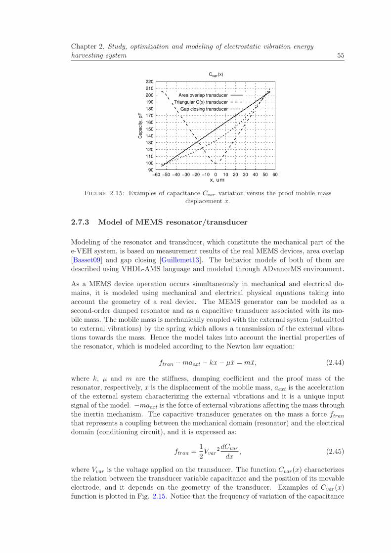
Figure 3: REV capacitif: a) architecture typique, b) trois exemples de car-acteristiques Cvar(x).
a) b) c) x
x
l
w
d
0 x
l
w
d
0
Figure 4: Geometries des transducteurs capacitifs: a) transducteur a rapprochementdes plans (gap closing), b) transducteur lineaire a mouvement dans le plan (in-planearea overlap), c) transducteur a mouvement dans le plan ayant une caracteristique
Cvar(x) de type dent de scie.
temps, le transducteur genere entre ses electrodes une force mecanique qui s’appliquea la masse. Cette force depend de la tension (charge) aux bornes de la capacite dutransducteur. De cette maniere, un transducteur electrostatique assure un couplagebidirectionnel entre les domaines mecanique et electrique.
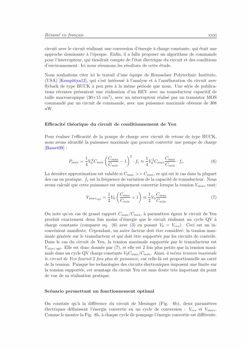
Un transducteur capacitif est caracterise par la relation entre la position de l’electrodemobile x et la valeur de sa capacite, Cvar(x). Cette fonction depend de la geometriedu transducteur: le plus souvent c’est une capacite plane dont une des electrodes sedeplace parallelement ou dans le sens normal par rapport aux plans. Fig. 3b presentetrois caracteristiques typiques des transducteurs capacitifs: une caracteristique hyper-bolique obtenue pour un transducteur a rapprochement normal des electrodes, une car-acteristique lineaire obtenue pour un transducteur a mouvement parallele de l’electrodemobile, et une caracteristique de type ”dent de scie” obtenue pour un transducteur amouvement parallele et a plusieurs segments (cf. Fig. 4).
Le transfert d’energie du domaine electrique vers le domaine mecanique s’effectue lorsque
Resume en francais xxiv
(a) (b) (c)
Figure 5: Trois cycles QV de conversion d’energie par un transducteur capacitif:a) cycle QV a charge constante, b) cycle QV obtenu avec circuit de conditionnement
primitif c) cycle QV obtenu avec une pompe de charge.
la capacite de transducteur diminue alors qu’elle reste chargee. L’energie W du trans-ducteur se calcule comme:
W = Q20/(2Cvar), (2)
ainsi, si le transducteur reste charge a la charge Q0 pendant que sa capacite diminue,l’energie electrique du transducteur augmente. En meme temps, dans le domaine mecanique,le transducteur genere une force mecanique sur la masse mobile. Cette force s’oppose aumouvement de la masse (c.a.d., la direction de la force est opposee a celle de la vitesse).Ainsi, le mouvement de la masse est amorti et le domaine mecanique perd de l’energie.
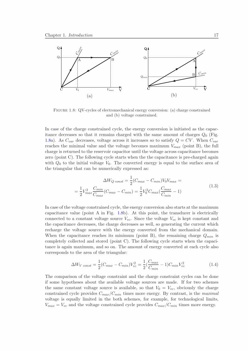
Ce processus de conversion d’energie se decrit par un diagramme designant l’ensembledes etats de la capacite variable dans les axes charge–tension (QV). Dans le cas d’unREV soumis aux vibrations periodiques, le diagramme QV est un cycle dont l’aire estnumeriquement egale a l’energie convertie durant ce cycle. Fig. 5a presente un exempledu cycle le plus commun qui s’appelle ”cycle a charge constante”. Les trois lignes ducycle correspondent au chargement du transducteur lorsque la capacite est maximale(CA), au mouvement de l’electrode mobile alors que la charge Q0 est gardee constante(AB) et a la decharge du transducteur (BC). D’apres la formule (2) on a pour le gaind’energie:
∆W =Q2
0
2Cmin−
Q20
2Cmax=
1
2Q2
0
(
1
Cmin−
1
Cmax
)
=1
2V 20 Cmax
(
Cmax
Cmin− 1
)
, (3)
ou V0 est la tension appliquee au transducteur lorsque sa capacite est maximale, V0 =Q0/Cmax. On note que pour une configuration de geometrie donnee, un seul parametreelectrique V0 (ou Q0) definit l’energie convertie. Ici Cmax et Cmin sont les valeursextremes que prend la capacite du transducteur durant le cycle. La puissance convertieest obtenue en multipliant ∆W par fe, la frequence de variation de la capacite. On noteque fe n’est pas forcement la meme que la frequence de vibration de la masse, au cas oula fonction Cvar(x) n’est pas monotone (cf. Fig. 3b).
Les Fig. 5b,c presentent deux autres exemples de cycles QV qui correspondent a d’autresprotocoles de conversion d’energie, et qui seront discutes a l’occasion des circuits deconditionnement qui leurs sont associes.
Resume en francais xxv
A partir de cette presentation, on peut tirer deux conclusions importantes. Premierement,la gestion de la charge–decharge du transducteur est necessairement complexe. En effet,ce processus doit etre strictement synchronise avec les mouvements de la masse mobile; ainsi, une mesure directe ou indirecte de la position de la masse est necessaire. Deplus, le cycle QV a charge constante necessite au moins deux commutations par periodede vibration. L’electronique de commande est donc complexe et couteuse en terme del’energie consommee [Mitcheson12]. La deuxieme conclusion concerne la necessite pourun transducteur capacitif d’avoir une precharge initiale (une energie initiale) permettantd’initier le processus de conversion d’energie.
Ces deux aspects mettent a part le transducteur capacitif par rapport a ces homo-logues piezoelectriques et electromagnetiques, qui generent une energie utilisable a par-tir du moment ou des vibrations sont presentes. Pour les REVs piezoelectriques etelectromagnetiques, le circuit de conditionnement sert essentiellement a assurer une in-terface electrique avec la charge utile tout en garantissant une extraction maximale del’energie mecanique [Lefeuvre09].
Circuit de conditionnement: principes et enjeux
Le role principal du circuit de conditionnement dans un REV capacitif est de charger etde decharger le transducteur capacitif selon un protocole assurant un cycle de conversiond’energie. Nous presentons ici une serie de circuits de conditionnement que nous avonsetudies durant nos recherches, pour aboutir a celui que nous avons choisi pour la basede nos developpements.
Circuit de conditionnement primitif
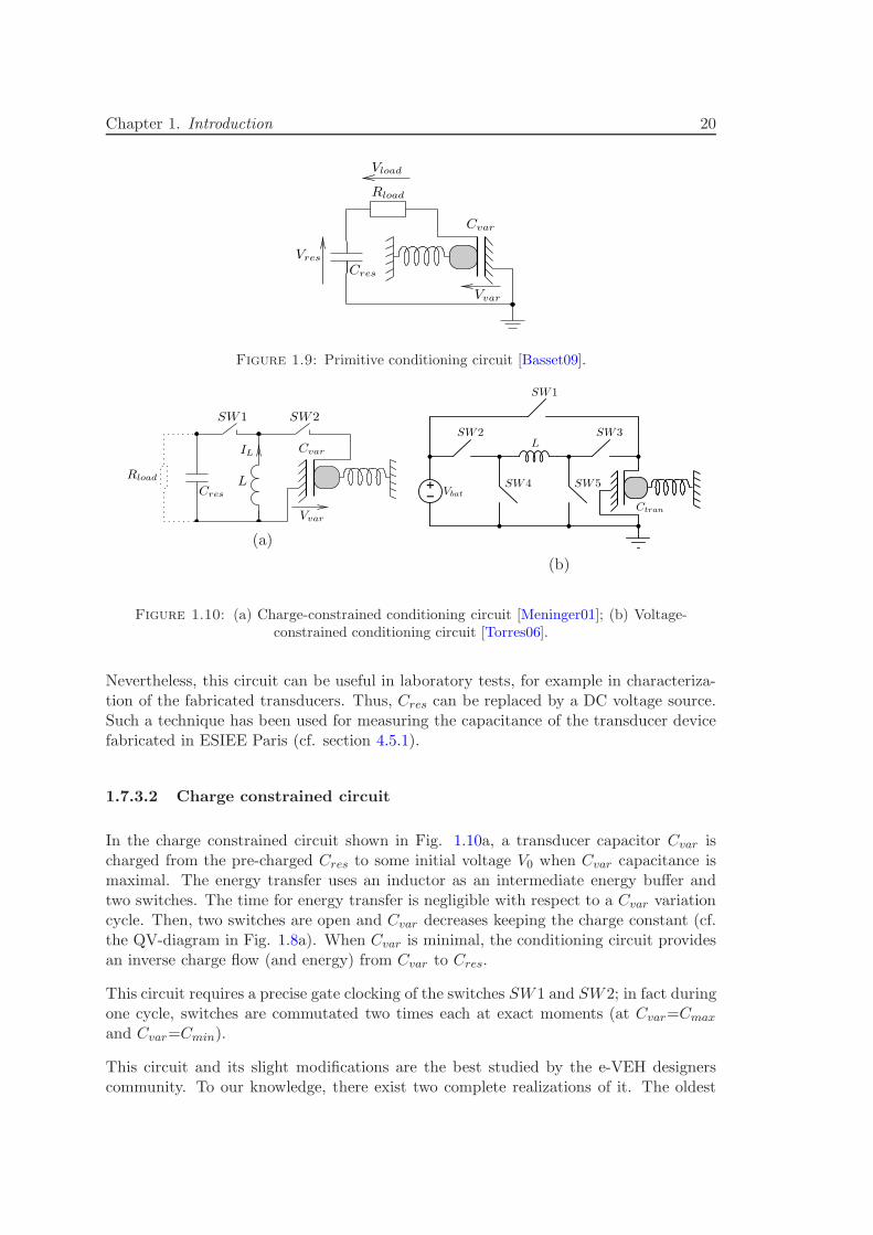
Il s’agit d’un systeme compose d’une capacite variable, d’une capacite de reservoir deforte valeur prechargee a tension V0 et d’une resistance de charge (Fig. 6a, [Basset09]).On peut voir que si la capacite Cvar varie, il y a un flux de charge entre Cvar et Cres;l’intensite de ce flux est fonction de la resistance Rload. Ce courant traversant uneresistance dissipe de l’energie: celle-ci est extraite du domaine mecanique grace auxvariations de la capacite Cvar . Le cycle QV realise par un transducteur conditionnepar ce circuit est donne Fig. 5b ; il est caracterise par sa trajectoire lisse (absenced’”angles”), le circuit ne contenant pas d’interrupteurs.
Le fonctionnement de ce circuit est base sur l’hypothese que la somme des charges deCvar et Cres est constante dans le temps. Autrement dit, on fait l’hypothese de l’absencede toute fuite sur ces deux capacites, ce qui est clairement pas realiste. Ainsi, ce circuitne presente pas d’interet applicatif. Cependant, il peut etre utile dans un contexte delaboratoire par exemple, pour une caracterisation d’un transducteur fabrique. Alors, lacapacite Cres peut etre remplacee par une source de tension continue. Cette techniquea ete utilisee pour caracteriser les dispositifs MEMS (micro resonateur avec interfacecapacitif) concus et fabriques a l’ESIEE Paris.
Un autre probleme de ce circuit est l’absence de mecanisme de precharge de la capaciteCres. En effet, il est connu qu’un transducteur capacitif necessite souvent des tensions de
Resume en francais xxvi
a) b)
Figure 6: a) Circuit de conditionnement primitif [Basset09]; b) Circuit de condition-nement realisant le cycle QV a charge constante [Meninger01].
polarisation elevees pour etre efficace (des dizaines des volts). Or, les tensions disponiblesinitialement dans un systeme autonome sont souvent basses (quelque volts). Ce circuitne contient pas de moyen permettant d’accroıtre sa tensions de polarisation a partird’une (faible) tension initiale.
Il faut ajouter que ce circuit se prete difficilement a une analyse. Par exemple, un calculanalytique de la resistance Rload correspondant a la puissance maximale est impossiblememe pour de simples configurations; il met en jeu une equation differentielle non lineairequ’il convient d’etudier en mode de grand signal. Il faut egalement ajouter que ce circuitretrouve son interet lorsqu’une couche d’electret est utilisee pour la polarisation initialede la capacite variable [Yamashita10, Sterken07, Boisseau11]. Par consequent, nousnotons un potentiel inexplore que peut contenir une etude analytique de ce circuit.
Circuit realisant un cycle a charge constante
Une architecture typique d’un circuit realisant le cycle triangulaire a charge constante(Fig. 5a) est donnee Fig. 6b. La capacite de reservoir Cres est prechargee. Lorsque lacapacite Cvar est maximale, une energie W0 est transferee de Cres a Cvar en utilisantL comme un reservoir d’energie intermediaire (il s’agit d’un procede typique pour con-vertisseurs DC-DC). Ceci est fait a l’aide des interrupteurs SW1 et SW2 commandespar un circuit de commande non montre ici. Le temps que prend ce transfert doit etrenegligeable compare a la periode de variation de Cvar. Ensuite les deux interrupteurssont bloques et Cvar diminue en gardant la charge constante. Lorsque Cvar arrive asa valeur minimale Cmin, le circuit de conditionnement effectue un transfert d’energieinverse de Cvar a Cres. Comme illustre par les formules (3) et (7), la capacite Cres recoitplus d’energie qu’elle ne contenait au debut.
A la difference avec le circuit precedent, les capacites Cvar et Cres s’echangent de l’energieet non des charges. Par consequent, il n’y a pas de problemes de fuites ; au contraire,les fuites de Cres sont assimilees a une charge utile connectee en parallele avec Cres (enpointillees).
Ce circuit realise le cycle QV a charge constante; il en possede dont les inconvenients.En particulier, on note un timing precis necessaire pour la commande des interrupteurs,et le fait d’avoir 4 commutations par cycle de variation de Cvar.
Resume en francais xxvii
Figure 7: Pompe de charge utilisee pour conversion d’energie mecanique enelectricite.
L’architecture presentee Fig. 6b et ses variantes sont les mieux etudiees par la com-munaute des concepteurs des REVs. Il existe, a notre connaissance, trois realisationscompletes et fonctionnelles de ce circuit. La premiere, la plus ancienne et la plus prochede l’architecture de la Fig. 6b est realisee a MIT2 par S. Meninger [Meninger01].Un autre circuit fonctionnant selon le meme principe a ete realise par G. Despesse[Despesse05]. Le circuit utilise un transformateur plutot qu’une inductance pour letransfert d’energie, et fonctionne avec un dispositif resonateur/transducteur de taillemacroscopique. Une des plus recentes realisations d’un REV de type a tension con-stante a ete presentee par E. Torres [Torres09]. Le systeme presente utilise une batteriea la place de la capacite reservoir Cres ; cela permet de recharger la batterie lorsqu’il ya des vibrations externes.
Pompe de charge comme circuit de conditionnement
Le probleme de la commande du flux des charges sur le transducteur est absent dansles circuits de conditionnement bases sur une pompe de charge (Fig. 7). Celle-ci estcomposee de deux diodes et trois capacites, dont l’une est une grande capacite reservoirCres, la deuxieme est une capacite de taille intermediaire Cstore, et la troisieme est lacapacite variable du transducteur, de valeur maximale la plus petite de trois:
Cres >> Cstore >> Cvar max (4)
A l’etat initial, la capacite reservoir est prechargee a la tension Vres = V0. Grace auxvariations de la capacite Cvar, les charges electriques se transferent de la capacite Cres
a la capacite Cstore. Un tel transfert des charges d’une grande capacite vers une petitecapacite s’accompagne d’une accumulation de l’energie electrique du systeme capacitifCstoreCres, en vertu de la formule (2). L’energie vient du domaine mecanique: ainsi unepartie de l’energie des vibrations externes est convertie en electricite.
Ce circuit tres simple a cependant un mecanisme de fonctionnement complexe. Nous endonnons ici quelques elements principaux.
Partant de l’etat initial correspondant a l’egalite des tensions Vres et Vstore, l’etat dusysteme CresCstore evolue comme presente Fig. 8. On y voit les tensions Vstore, Vres etl’energie ∆Wi convertie en chaque cycle de variation de Cvar. On constate que l’energie
2Massachusetts Institute of Technology
Resume en francais xxviii
a)
4.5
5
5.5
6
6.5
7
7.5
8
8.5
9
9.5
10
0 10 20 30 40 50 60 70 80
b)
0
5
10
15
20
25
30
35
40
45
0 10 20 30 40 50 60 70 80
0
0.2
0.4
0.6
0.8
1
1.2
1.4
Figure 8: Evolution de l’etat de la pompe de charge: a) Les tensions Vstore et Vres.Vstore evolue de la tension Vres (5V dans cet exemple) jusqu’a la tension de saturation(10 V dans cette exemple), Vres ne change presque pas (Cres est large) b) l’energie
convertie par cycle de vibration ∆Wi et depuis le debut du pompage Wi
convertie par cycle augmente au debut, atteint un maximum et puis diminue jusqu’azero. En meme temps, la tension Vstore tend asymptotiquement vers une valeur appelee”tension de saturation” egale a:
Vstore sat = VresCmax
Cmin. (5)
Lorsque la pompe de charge est saturee, il n’y a plus de conversion d’energie. Il est doncnecessaire de retourner la pompe de charge vers un etat ou la generation d’energie estproche du maximum. D’apres la Fig. 8, il s’agit de reduire la tension Vstore. Cela estfait a l’aide d’un circuit de retour (flyback) dont deux versions sont presentees dans lesdeux sections suivants.
Circuit de retour resistif
Un circuit de retour elementaire est realise par une resistance branchee entre Cres etCstore (Fig. 9). Dans ce cas, il y a deux flux de charges: l’un, source d’energie electrique,de Cres vers Cstore pousse par les variations de Cvar, l’autre, consommateur d’energieelectrique, celui de la resistance RL. En regime etabli, il est possible de choisir unevaleur Rload pour laquelle la puissance d’energie convertie est optimale (i.e., correspondau maximum de ∆Wi a la Fig. 8b). La resistance Rload peut etre vue comme une chargeutile.
Les faiblesses de ce circuit sont similaires a celles du circuit de la Fig. 6a : son fonc-tionnement est base sur l’hypothese de l’absence de fuites dans les capacites. Dansle cas contraire, la precharge de Cres finit par devenir nulle et le circuit devient inac-tif. Ce probleme peut etre resolu par des techniques de compensations proposees parH.R. Florentino [Florentino11]. Il y est propose d’adjoindre un generateur d’energiesupplementaire a base d’un transducteur piezoelectrique, qui compenserait les pertesdans les capacites. Alors que cette solution peut etre envisageable dans certains cas,elle n’est cependant pas tres commode, car cela revient a utiliser deux REVs dont l’unalimente l’autre. Une des difficultes que l’on y voit est un necessaire accord en frequencedes deux resonateurs, ce qui est difficile en pratique car les bases technologiques pourleur fabrication sont necessairement differentes.
Resume en francais xxix
Figure 9: Pompe de chargeavec un circuit de retour
resistif.
Figure 10: Circuit de condition-nement a base de la pompe de chargeutilisant un circuit de retour de typeconvertisseur DC-DC BUCK, pro-
pose par Yen [Yen06].
On note une absence du mecanisme d’elevation de la tension de polarisation, de memeque pour le circuit de conditionnement primitif de la Fig. 6a.
Ces difficultes nous amenent au circuit de retour de type convertisseur DC-DC de typeBUCK qui est exempt des inconvenients mentionnes.
Circuit de conditionnement propose par Yen
Ce circuit a ete propose par B. C. Yen et J. H. Lang en 2006 a MIT [Yen06], sonschema est donne Fig. 10. Le circuit de retour est base sur un convertisseur DC-DCde type BUCK. Ce circuit de conditionnement fonctionne en deux phases. Durant lapremiere phase, l’interrupteur SW est bloque et seule la pompe de charge fonctionnecomme presente plus haut. Ensuite, lorsque la pompe de charge approche la saturation(Vstore = V2), un circuit de commande (non montre) rend l’interrupteur passant, enactivant le circuit de retour. Le retour se fait en deux etapes. D’abord, une partie decharges de Cstore retourne vers Cres, en abaissant ainsi la tension de Cstore. Pendantce processus, la capacite Cres retrouve ses charges, et l’energie transferee du domainemecanique est emmagasinee dans l’inductance L. Lorsque la tension Vstore a baissejusqu’a V1, l’interrupteur se bloque et l’inductance se decharge sur la capacite Cres viala diode D3 empechant un retour de charges. Puis le cycle recommence (Fig. 11).
Ce fonctionnement presente une serie d’avantages qui nous ont fait choisir ce circuitcomme base pour notre etude.
a) Accumulation de l’energie convertie. En absence de charge utile, l’energie converties’accumule sur la capacite Cres. Il est donc possible d’elever sa tension jusqu’au niveaunecessaire, en demarrant par une faible precharge qui peut etre fournie avec une sourcede tension existante dans le systeme.
b) Presence d’un seul interrupteur fonctionnant rarement et qui ne necessite pas unesynchronisation avec les mouvements de la masse. L’interrupteur commute une foisdurant plusieurs periodes de vibration de la masse: donc, la commande se fait a des
Resume en francais xxx
a)
5
6
7
8
9
10
0 0.05 0.1 0.15 0.2 0.25 0.3 0.35
Volts
time, s
store with flyback
store without flyback
1
2
store max
V
V
V
V
V
b)
0
100
200
300
400
500
0 0.05 0.1 0.15 0.2 0.25 0.3 0.35
nW
atts
time, s
Cycle power with flyback
Cycle power without flyback
Figure 11: Evolution de l’etat de la pompe de charge avec circuit de retour: a) Latension Vstore. b) Puissance moyenne de conversion d’energie par cycle de vibration
∆Wi.
frequences bien plus basses que dans le cas du circuit de Meninger (Fig. 6b). Moinsd’energie est donc necessaire pour la commande.
c) La commutation pompe de charge/circuit de retour se fait en fonction de la valeur dela tension Vstore. Il est en effet bien plus simple d’utiliser une tension pour le controle,plutot qu’une valeur de capacite ou une grandeur mecanique.
Ce sont surtout les deux derniers points qui nous ont fait choisir ce circuit pour la basede nos developpements pratiques d’un REV capacitif avec conditionnement intelligent.Les problemes associes a ce travail et le resume des resultats sont presentes dans lasuivante section.
Circuit de conditionnement adaptatif integre
Ce paragraphe resume nos idees sur le circuit de conditionnement adaptatif et intelligent,et resume nos travaux de conception d’un circuit de demonstrateur.
Analyse du circuit de Yen: recherche du fonctionnement optimal
L’article de Yen publie en 2006 [Yen06] presente un premier demonstrateur d’un circuitde conditionnement base sur la pompe de charge et utilisant un circuit de retour de typeBUCK DC-DC. L’interrupteur SW est realise par un transistor MOS commande par unesource externe. Cette source genere un train periodique d’impulsions independantes del’etat du circuit. Cette experience a demontre la faisabilite de cette technique. Cepen-dant, ce travail a ouvert un vaste champs de problemes, notamment, en ce qui concerne ladefinition d’un regime optimal et la conception d’une commande garantissant ce regime.La theorie du circuit etait incomplete: par exemple, il manquait une expression de lapuissance maximale convertible par ce circuit. Il n’etait alors pas possible d’etablir unecomparaison des performances avec le circuit realisant un cycle QV charge constante(circuit de la Fig. 6b).
Afin de combler ces lacunes, la premiere etape a ete d’analyser le circuit en identifiant desconditions optimales de fonctionnement. Il etait egalement important de comparer ce
Resume en francais xxxi
circuit avec le circuit realisant une conversion d’energie a charge constante, qui etait uneapproche dominante a l’epoque. Enfin, il a fallu proposer un algorithme de commandepour l’interrupteur, qui tiendrait compte de l’etat electrique du circuit et des conditionsd’environnement. Ici nous resumons les resultats de cette etude.
Nous souhaitons citer ici le travail d’une equipe de Rensselaer Polytechnic Institute,(USA) [Kempitiya12], qui s’est interesse a l’analyse et a l’amelioration du circuit avecflyback de type BUCK a peu pres a la meme periode que nous. Une serie de publica-tions recentes presentent une realisation d’un REV avec un transducteur capacitif detaille macroscopique (30×15 cm2), avec un interrupteur realise par un transistor MOScommande par un circuit de commande, avec une puissance maximale obtenue de 308nW.
Efficacite theorique du circuit de conditionnement de Yen
Pour evaluer l’efficacite de la pompe de charge avec circuit de retour de type BUCK,nous avons identifie la puissance maximale que pouvait convertir une pompe de charge[Basset09] :
Pmax =1
4V 20 Cmin
(
Cmax
Cmin− 1
)2
· fe ≈1
4V 20 Cmax
Cmax
Cmin· fe. (6)
La derniere approximation est valable si Cmax >> Cmin, ce qui est le cas dans la plupartdes cas en pratique. fe est la frequence de variation de la capacite de transducteur. Nousavons calcule que cette puissance est uniquement convertie lorsque la tension Vstore vaut:
Vstoreopt =1
2V0
(
Cmax
Cmin+ 1
)
≈1
2V0
Cmax
Cmin(7)
On note qu’en cas de grand rapport Cmax/Cmin, a parametres egaux le circuit de Yenproduit exactement deux fois moins d’energie que le circuit realisant un cycle QV acharge constante (comparer eq. (6) avec (3) en posant V0 = Vres). Ceci est un in-convenient manifeste. Cependant, un autre facteur doit etre considere: la tension max-imale generee sur le transducteur et qui doit etre supportee par les circuits de controle.Dans le cas du circuit de Yen, la tension maximale supportee par le transducteur estVstore opt. Elle est donc donnee par (7), et elle est 2 fois plus petite que la tension maxi-male dans un cycle QV charge constante V0Cmax/Cmin. Ainsi, a meme tension maximalele circuit de Yen fournit 2 fois plus de puissance, car celle-la est proportionnelle au carrede la tension. Puisque les technologies des circuits electroniques imposent une limite surla tension supportee, cet avantage du circuit Yen est sans doute tres important du pointde vue de sa realisation pratique.
Scenario permettant un fonctionnement optimal
On constate qu’a la difference du circuit de Meninger (Fig. 6b), deux parametreselectriques definissent l’energie convertie en un cycle de conversion : Vres et Vstore.Comme le montre la Fig. 8b, a chaque cycle de pompage l’energie convertie est differente.
Resume en francais xxxii
Figure 12: Automate d’etats finis regissant le fonctionnement de l’interrupteur ducircuit de retour.
Elle n’est maximale que pour la valeur Vstore donnee par l’expression (7), qui est respecteeuniquement sur un cycle de pompage. Ainsi, garantir un fonctionnement optimal a cecircuit revient a activer le circuit de retour une fois par cycle de variation de Cvar.Ceci est possible si le circuit de retour est realise par une resistance (cf. Fig. 9): cettetechnique a ete utilisee pour tester les dispositifs MEMS fabriques a l’ESIEE Paris parRaphael Guillemet [Guillemet13]. Cependant, dans le cas d’utilisation du circuit de re-tour de type BUCK, cela fait perdre les avantages principaux de l’architecture, qui sontl’absence de synchronisation du retour des charges/energie avec les mouvements de lamasse et une faible frequence de ces retours.
Pour trouver un compromis entre la maximisation de la puissance convertie et le coutd’activation du circuit de retour, nous avons propose de maintenir la puissance convertiea un certain niveau ne depassant pas le niveau maximal moins quelques pour cents,comme c’est affiche sur la courbe ∆Wi de la Fig. 11b. Cela permet de definir unintervalle des valeurs de Vstore pour lesquelles le circuit peut fonctionner en mode optimal(V1, V2) (Fig. 11a), et ainsi de definir les moments de commutation de l’interrupteur enmesurant la tension sur une grande capacite Cstore, plutot qu’en detectant les extremade variation de la faible capacite Cvar [Galayko07]. Nous avons etabli une equationempirique permettant une estimation de seuils de commutation:
Il est maintenant possible de construire un automate d’etats finis qui commandera l’etatde l’interrupteur. Cet automate est commande par les evenements de croisement desseuils V1 et V2 par la tension Vstore. Le diagramme de l’automate est presente Fig. 12.
Besoin d’autocalibration
Les points 1) et 2) presentes dans la sous-section precedente amenent sur la conclusionsuivante: l’intervalle des valeurs optimales de (V1, V2) est defini par Vres et la tensionde saturation de la pompe de charge qui depend de Cmax/Cmin. Alors que Vres semesure sans difficulte, les valeurs Cmax et Cmin dependent, en general, de l’amplitudedes vibrations. Par exemple, au cas ou la fonction Cvar(x) est de type hyperbolique
Resume en francais xxxiii
Flyback adaptive switch control
Electrical switch behavioral model
Process 1
Calibration block
Process 2
Process 3
Process 4
Process 5
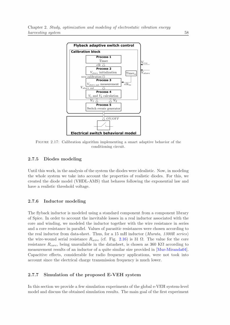
Figure 13: Algorithme de fonctionnement du circuit de conditionnement intelligent[Dudka09b].
(transducteur a rapprochement des electrodes, Cmax et Cmin sont definis comme :
Cmax,min = ǫ0S
d−X0 ±X1
(9)
ou X0 est une eventuelle position moyenne de la masse mobile, X1 est l’amplitude desmouvements de la masse.
Les parametres X0 et X1 dependent des parametres des vibrations externes (l’amplitudeet la frequence) qui sont sujettes aux variations. De meme, les parametres du systeme nesont connus qu’avec une certaine precision, notamment, les parametres du resonateur etdu transducteur. Ainsi, a priori, il n’est pas possible de connaıtre le rapport Cmax/Cmin,et donc, de trouver les valeurs V1 et V2 optimales dans un contexte pratique.
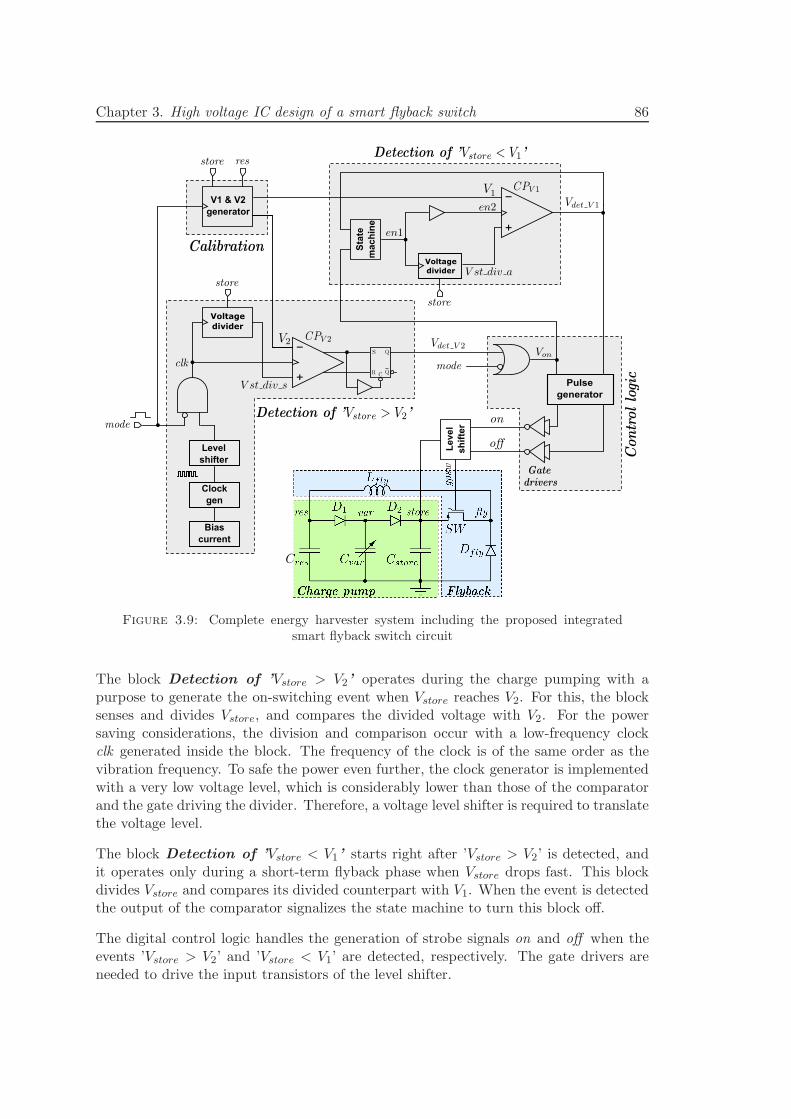
Ces conclusions mettent en evidence la necessite de prevoir un systeme d’autocalibrationpour un REV utilisant le circuit de Yen. Cette autocalibration doit se faire periodiquement,tout au long du fonctionnement du circuit, car l’amplitude des vibrations externes estsusceptible de changer a tout moment. Durant la phase d’autocalibration, la mesure deCres/Cstore peut se faire a travers la mesure de la tension de saturation de la pompede charge. Pour cela on doit desactiver le circuit de retour et laisser evoluer la tensionVstore selon la courbe de la Fig. 8a, tout en detectant la saturation et en mesurant lavaleur Vstore sat (cf. eq. 5). Cet algorithme propose dans cette these est presente a laFig. 13, [Dudka09b]. Il est a la base d’un modele VHDL-AMS utilise pour la conceptiondu circuit.
A partir de ces reflexions, nous avons etabli un cahier de charge pour le circuit decommande du circuit de conditionnement de Yen.
Resume en francais xxxiv
Power-to-
analog
interfaceADC MP
Switch
interface
Figure 14: Architecture generique d’un circuit de conditionnement intelligent.
Circuit de conditionnement et intelligence
L’etude du circuit de Yen presentee ci-dessus suggere que le circuit de conditionnementdoit etre adaptatif. Il s’agit d’une fonction ”intelligente” qui suppose un traitementd’information complexe, necessairement consommateur d’energie. L’adaptation doitdependre du contexte applicatif et globalement, doit pouvoir gerer le flux d’energieexterieur disponible - par exemple, faire ”endormir” le systeme si l’energie disponibleest trop faible.
Pour ces raisons, nous contestons la vision des dispositifs de recuperation d’energie vi-bratoire comme etant primitifs et necessitant des solutions analogiques optimisees ad hocpour un contexte particulier. Nous pensons que les REVs ne peuvent devenir reellementpertinents pour les applications que s’ils integrent une complexite et une intelligence. Al’etat actuel des technologies, cette vision est peu realiste: la puissance delivree par lesmicro generateurs etant de quelques microwatt, ce niveaux est a peine suffisant pour ali-menter la charge utile (c.a.d., le fonctionnement de l’application). Cependant, les etudessur la recuperation d’energie a micro echelle sont basees sur un pari selon lequel dansle futur, les niveaux d’energie requis par les microsystemes electroniques de traitementcontinueront a baisser. Ainsi, arrivera un moment ou l’intelligence se trouvant dans lecircuit de conditionnement ne necessitera qu’une petite partie de l’energie recuperee.Cela a motive et justifie notre etude, dans laquelle nous avons propose et developpe uneapproche de la conception d’un systeme de REV capacitif avec comportement complexeet auto adaptatif.
Cette vision idealisee et futuriste de circuit de conditionnement intelligent est donneeFig. 14, qui presente une boucle de contre-reaction prenant la mesure des tensionsVres et Vstore. Les resultats de ces mesures sont numerises et analyses par un bloc detraitement numerique represente ici par un microprocesseur (MP), qui ensuite genereune commande pour l’interrupteur.
Les recherches sur le developpement d’un circuit de conditionnement adaptatif et intel-ligent sont les objectifs principales de cette these. Pour atteindre ces objectifs, ce travails’est fait en deux etapes: conception d’un algorithme de fonctionnement du circuit etconception du circuit realisant cet algorithme. Dans les sous-sections suivantes nouspresentons les problemes auxquels nous avons ete confrontes et les choix strategiquesque nous avons faits.
Resume en francais xxxv
VHDL-AMS/SPICE model
[Galayko et al., BMAS 2007]
State
automaton
VHDL-AMS model
[Dudka et al., BMAS 2009]
Auto-calibration
module
Figure 15: Architecture du circuit de conditionnement developpe, avec mention desoutils de modelisation utilises pour chaque partie.
Circuit de conditionnement auto adaptatif: architecture
Une conception au niveau de systeme a ete la premiere etape du developpement. Ils’agit d’une elaboration de l’algorithme de calibration, d’un choix de l’architecture ducircuit de commande et d’une validation par modelisation comportementale du systemede REV complet.
L’idee de base consiste a entrecouper la phase de conversion d’energie par des phasesd’autocalibration. L’hypothese suivante a ete faite: les parametres d’environnementsont supposes evoluer lentement, et donc les valeurs V1 et V2 trouvees lors d’une phased’autocalibration restent actuelles jusqu’a la prochaine phase. La vitesse d’evolutiondes conditions d’environnement determine la frequence avec laquelle il faut calibrer lecircuit. Cette frequence depend du contexte applicatif, et peut aller de quelques secondesa quelques minutes.
Fig. 15 presente l’architecture du circuit de conditionnement adaptatif que nous avonsdeveloppe [Dudka09a], avec l’indication des outils permettant une modelisation de chaquebloc. L’etude qui a permis un choix approprie des outils de modelisation est resumeedans une des sections suivantes.
Conception de circuit integre
La deuxieme etape consiste a concevoir un circuit electronique realisant cette architec-ture. L’objectif etant la miniaturisation, le circuit de conditionnement doit etre integresur silicium autant que possible. Sans rentrer dans les details de la conception, donnesdans nos articles [Dudka09b, Dudka12, Dudka13b], nous enumerons les verrous auxquelsnous etions confrontes.
• Hautes tensions necessaires pour le fonctionnement du transducteur electrostatique.La plus grande difficulte de ce projet resulte des hautes tensions auxquelles fonc-tionne le circuit de conditionnement. Nous nous sommes donnes une limite de 50V pour la tension maximale que ce circuit doit pouvoir supporter (les tensions sur
Resume en francais xxxvi
Figure 16: Illustration du probleme de la commande d’un interrupteur ”flottant”haute tension.
(a) (b)
Figure 17: Circuit de commande de l’interrupteur avec un nouveau elevateur detension, circuit realise en technologie AMS035HV [Dudka12]: (a) schema (b) layout.
le transducteur et sur Cstore). Les difficultes mentionnees plus bas sont toutes plusou moins liees a cette contrainte.
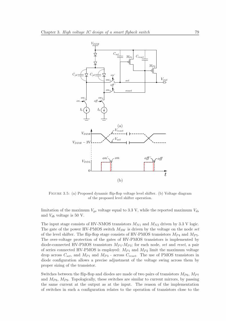
• L’interrupteur SW flottant a haute tension. L’interrupteur SW n’est pas raccordea la masse: lorsqu’il est coupe, il subit une tension flottante. Cet interrupteurest realise par un transistor PMOS haute tension, dont la tension de commandedoit etre generee par rapport a la haute tension de la source du transistor (cf.Fig. 16). Un elevateur de tension (level shifter) est donc necessaire, avec unecontrainte de consommation statique proche de zero. Cette difficulte est un desplus etroits goulets d’etranglement de ce projet, car le cout energetique de lacommutation de SW a un role central dans l’efficacite de la conversion d’energiepar le circuit. La conception d’un elevateur de tension ultra basse consommationa ete effectuee avec succes en s’inspirant de l’architecture utilisee par P. Basset[Basset03]. Un prototype integre de l’interrupteur associe au dispositif de controleet de l’elevateur de tension ultra basse consommation (cf. Fig. 17) a ete realise,fabrique en technologie 0.35 µm haute tension et teste.
Resume en francais xxxvii
• Une large plage de la tension de fonctionnement. Comme il a ete mentionne, audemarrage le circuit de conditionnement possede une energie fournie par le systeme.Ainsi, les tensions Vres et Vstore sont basses au debut, avec Vres ≈ 2 − 3 V, etVstore:;max ≈ 6− 10 V. En regime optimal, selon les parametres des vibrations ex-ternes, la tension Vstore peut atteindre la valeur maximale autorisee par le systeme(50 V ). Ainsi, le circuit de commande doit etre efficace pour toute la gamme destensions de fonctionnement, ce qui est difficile a atteindre. Par exemple, pourmesurer les hautes tensions Vres et Vstore, la premiere approche consiste a utiliserdes diviseurs a base de diodes ou transistors MOS en regime sous le seuil. Cepen-dant, compte tenu de la plage de tensions a mesurer (facteur min/max de 5), cettesolution ne convient pas. L’utilisation des resistances de tres haute valeur s’imposealors, ce qui oblige a utiliser des resistances discretes [Dudka12].
• La contrainte ultra basse consommation. Un des objectifs de l’etude est d’estimerle niveau de consommation minimale que peut avoir un circuit de conditionnementintelligent comme celui de la Fig. 15. A priori, il etait difficile de se donner unchiffre plafond precis. Neanmoins, on peut dire que la consommation des blocs ducircuit de conditionnement ne doit pas depasser 1−3 µW . C’est une contrainte tresforte qui a marque la plupart des choix d’architecture. Par exemple, la division deshautes tensions pour la mesure se fait non pas en continu, mais par echantillonnage.
Le circuit complet concu au niveau transistor est donne Fig. 3.9. Ce circuit est valide parsimulation de son modele ELDO (Spice) dans le contexte du modele VHDL-AMS/ELDOmixte du recuperateur (Fig. 15). Les performances sont satisfaisantes, en particulier,la consommation moyenne est entre 1 et 2 µW , selon le regime electrique. Il utilisela technologie CMOS 0.35 haute tension d’Austria Microsystems. Compte tenu de lamaturite de cette technologie et par consequent de la fiabilite des modeles de transistors,nous avons un haut degre de confiance en resultats de simulation.
Conception du circuit de conditionnement: travaux futurs
Pour que la preuve de concept soit complete, les questions suivantes doivent etre abordeesdans la suite de l’etude.
Les blocs ”peripheriques” necessaires au fonctionnement autonome du circuit. Il s’agitdes sources d’alimentation, de polarisation et d’horloge. Ces fonctionnalites sont pri-mordiales pour tout circuit integre. Or, dans le contexte de la recuperation d’energie,la conception des blocs peripheriques represente un projet de recherche a part entiere.En effet, le REV est un systeme auto alimente: amorce par une energie fournie par lesysteme, il doit procurer l’energie pour son alimentation a partir de son propre fonction-nement. Une solution possible a ete proposee dans cette these, permettant de genererune (basse) tension d’alimentation stable a partir de la tension de la capacite Cres quipeut varier de 3 a 15 V [Dudka09a]. Cette solution n’a pas encore ete realisee au niveaudes transistors: cette tache sera l’objet des travaux futurs.
Le circuit de conditionnement de la Fig. 3.9 necessite deux horloges de basse frequence:l’une a le meme ordre de grandeur que la frequence des vibrations (≈100 Hz), l’autredoit permettre de cadencer la succession des phases de calibrations et a donc une periode
Resume en francais xxxviii
−
+
−
+
Le
ve
l
sh
ifte
r
Clock
gen
Sta
te
ma
ch
ine
V1 & V2
generator
Voltage
divider
Voltage
divider
Level
shifter
Bias
current
Pulse
generator
Figure 18: Schema electrique du circuit de conditionnement intelligent concu[Dudka13b].
de 1 a 100 secondes. Une etude bibliographique sur le sujet a mis en evidence un grandinteret de la communaute envers de tels circuits, pour les applications de type capteursautonomes et systemes biomedicaux embarques dans du vivant. Par exemple, un capteurse trouvant en veille et devant s’activer de temps en temps a besoin d’une telle horloge.Ici, la contrainte principale est la basse consommation, qui doit etre respectee quitte asacrifier la precision du timing. Une premiere approche de ce travail ete faite dans lecadre du stage de master recherche d’Anthony Deluthault a LIP6.
Interface avec la charge. Le probleme de generation d’une alimentation stable bassetension pour les circuits de traitement est lie a un probleme plus fondamental, celui del’interface avec une charge utile. Cela inclut au minimum une generation de tensionstable qui peut etre utilisee par la charge. De plus, il est necessaire de proposer unmecanisme capable de gerer une situation ou l’energie disponible ne serait pas suffisantepour alimenter la charge. Ce probleme a ete aborde durant cette these. Il a ete proposede reutiliser le convertisseur DC-DC du circuit de retour afin de generer une tensionde sortie stable. Il s’agit d’un convertisseur DC-DC a sorties multiples: une structurefrequemment utilisee dans les circuits d’alimentation multi tensions. Le principal avan-tage de cette solution est la reutilisation de l’inductance L deja presente dans le circuitde retour [Dudka09a].
Resume en francais xxxix
Modelisation des REVs
Motivations
Les techniques de modelisation occupent une place centrale dans la conception de cir-cuits et systemes electroniques, principalement, a cause du cout eleve du prototypagephysique, de la complexite des systemes et de la puissance des calculateurs actuels. Laparticularite de nos problemes vient du caractere multidisciplinaire du systeme, et del’heterogeneite des signaux qui y sont presents. On s’interesse a la modelisation pour lesobjectifs suivants:
– Une exploration du systeme. Une modelisation comportementale represente un ex-cellent outil d’experimentation virtuelle, lorsqu’il s’agit de repondre rapidement a unequestion relative au comportement du systeme dans un contexte particulier. Ainsi, ladecouverte des regimes stochastiques et irreguliers [Galayko11b] du REV de la Fig. 6ba ete faite grace a la modelisation comportementale.
– La conception du systeme et de ses blocs. La methodologie dominante de conceptionest ”top-down”: cela signifie que d’abord le systeme est concu sur le plan fonctionnel, ahaut niveau d’abstraction. Ensuite chaque bloc/fonction sont concus d’une maniere deplus en plus detaillee, jusqu’au niveau des composants elementaires de la technologie.La modelisation accompagne ce processus en descendant les niveaux d’abstraction, afinde valider chaque etape de conception.
Les specificites de la micro fabrication font que les concepteurs des MEMS ont moinsde libertes de conception que les concepteurs de circuits electriques et de logiciels. Pourcette raison, souvent un dispositif MEMS existant constitue une donnee lors de la con-ception du systeme. Dans notre projet, les dispositifs MEMS constitues d’un resonateurassocie a un transducteurs ont ete fabriques et caracterises par le groupe de PhilippeBasset a l’ESIEE Paris. Nous avons construit des macromodeles de ces dispositifs etnous les avons ensuite utilises dans le modele du systeme global.
Choix de la plate-forme
La question que nous nous sommes pose au debut du projet concerne le choix de laplate-forme de modelisation. Une etude comparative a ete faite par Ken Caluwaertsdans le cadre de son stage de master recherche a LIP6, au cours duquel trois envi-ronnements ont ete testes pour une modelisation du systeme presente Fig. 15 : Mat-lab/Simulnk, SystemC-AMS et la plate-forme AdvanceMS de Mentor Graphics. Laplate-forme SystemC-AMS etait, a l’epoque, une nouveaute dans l’univers de modelisationde systemes heterogenes, et elle etait en pleine evolution. Etant une plate-forme libre, ellesuscitait un grand interet dans la communaute de concepteurs de systemes electroniques.Nous avons voulu evaluer son potentiel pour la modelisation de systemes de REV, surl’exemple du systeme de la Fig. 15.
Resume en francais xl
La version de l’epoque (2008) de la plate-forme SystemC-AMS s’est averee peu adapteea la simulation de systeme de ce type3, principalement, en raison du nombre limite demethodes de resolution d’equations non lineaires qu’elle offrait. En effet, la plate-forme autilise des methodes d’integration a pas temporel fixe, ce qui etait un facteur fortementlimitant pour les systemes fonctionnant simultanement a multiples echelles de tempscomme dans le cas d’un systeme de REV.
C’etait la plate-forme AdvanceMS de Mentor Graphics qui s’est averee le plus appro-priee pour nos besoins. Elle permet de melanger les modeles VHDL-AMS (analogiquescomportementaux), VHDL (numeriques) et ELDO (une variante commerciale de SPICEdeveloppee par Mentor Graphics), et offre une large palette des methodes numeriquespour l’integration des equations du systeme [Pecheux05]. De plus, l’interface utilisateurest bien plus evoluee que celle des deux autres plates-formes testees. C’est donc cet outilqui a ete choisi pour la simulation et la conception de nos REVs.
Modelisation du bloc transducteur/resonateur
Un transducteur capacitif est modelise par un systeme de ses equations :
ivar =dqvardt
, qvar = Cvar(x)Vvar), fvar =1
2V 2var
dCvar
dx(10)
Ici qvar est la charge electrique du transducteur, ivar est le courant qui le traverse, xest la position de l’electrode mobile. Cvar(x) est une fonction connue caracterisant larelation entre la capacite du transducteur et la position de son electrode mobile.
Ces trois dernieres equations possedent 5 inconnues: qvar, ivar , Vvar, fvar et x. Lesdeux relations manquantes doivent etre definies par les sous-systemes mecaniques etelectriques associes au transducteur. Du cote mecanique, l’equation manquante estdonnee par celle du sous-systeme mecanique. En prenant comme exemple un resonateurdu second ordre avec une masse m, un amortissement µ et une constante de raideur k,on a :
−µx− kx+ fvar + Fext = mx, (11)
Ici Fext est la force generee par les vibrations exterieures. Elle est egale a −maext, ouaext est l’acceleration connue des vibrations exterieures. Cette equation est facilementadaptable aux differents types de structures mecaniques analysees.
Le systeme (10), (11) pour etre complet ne necessite plus qu’une relation, celle entreles grandeurs electriques. Celle-ci est fixee par le circuit qui est connecte aux borneselectriques du transducteur. Ainsi, le modele du systeme ”resonateur–transducteur” estpresente comme un dipole electrique, pret a etre utilise dans un modele de type Spice.
3Depuis cette etude, la plate-forme SystemC-AMS a beaucoup evolue, et notre experience n’est plusrepresentative de la realite.
Resume en francais xli
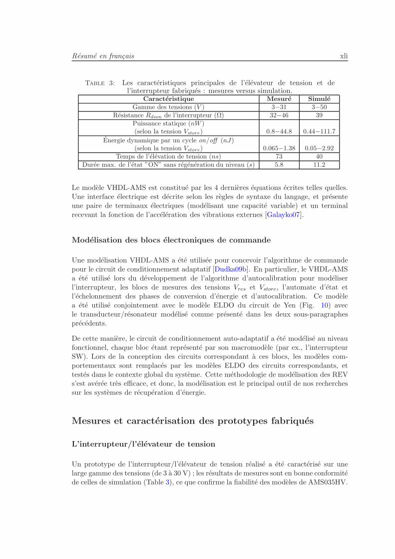
Table 3: Les caracteristiques principales de l’elevateur de tension et del’interrupteur fabriques : mesures versus simulation.
Caracteristique Mesure SimuleGamme des tensions (V ) 3−31 3−50
Resistance Rdson de l’interrupteur (Ω) 32−46 39Puissance statique (nW )(selon la tension Vstore) 0.8−44.8 0.44−111.7
Energie dynamique par un cycle on/off (nJ)(selon la tension Vstore) 0.065−1.38 0.05−2.92
Temps de l’elevation de tension (ns) 73 40Duree max. de l’etat ”ON” sans regeneration du niveau (s) 5.8 11.2
Le modele VHDL-AMS est constitue par les 4 dernieres equations ecrites telles quelles.Une interface electrique est decrite selon les regles de syntaxe du langage, et presenteune paire de terminaux electriques (modelisant une capacite variable) et un terminalrecevant la fonction de l’acceleration des vibrations externes [Galayko07].
Modelisation des blocs electroniques de commande
Une modelisation VHDL-AMS a ete utilisee pour concevoir l’algorithme de commandepour le circuit de conditionnement adaptatif [Dudka09b]. En particulier, le VHDL-AMSa ete utilise lors du developpement de l’algorithme d’autocalibration pour modeliserl’interrupteur, les blocs de mesures des tensions Vres et Vstore, l’automate d’etat etl’echelonnement des phases de conversion d’energie et d’autocalibration. Ce modelea ete utilise conjointement avec le modele ELDO du circuit de Yen (Fig. 10) avecle transducteur/resonateur modelise comme presente dans les deux sous-paragraphesprecedents.
De cette maniere, le circuit de conditionnement auto-adaptatif a ete modelise au niveaufonctionnel, chaque bloc etant represente par son macromodele (par ex., l’interrupteurSW). Lors de la conception des circuits correspondant a ces blocs, les modeles com-portementaux sont remplaces par les modeles ELDO des circuits correspondants, ettestes dans le contexte global du systeme. Cette methodologie de modelisation des REVs’est averee tres efficace, et donc, la modelisation est le principal outil de nos recherchessur les systemes de recuperation d’energie.
Mesures et caracterisation des prototypes fabriques
L’interrupteur/l’elevateur de tension
Un prototype de l’interrupteur/l’elevateur de tension realise a ete caracterise sur unelarge gamme des tensions (de 3 a 30 V) ; les resultats de mesures sont en bonne conformitede celles de simulation (Table 3), ce que confirme la fiabilite des modeles de AMS035HV.
Resume en francais xlii
−
+
−
+
+−
Reso
nato
r/
tran
sd
ucer
Flyback
switch
Pre-charge
of the system Charge pump Flyback
External
control logic
O-scope O-scope
Figure 19: Schema d’un REV etudie et micro-photographie du bloc del’interrupteur/driver fabrique.
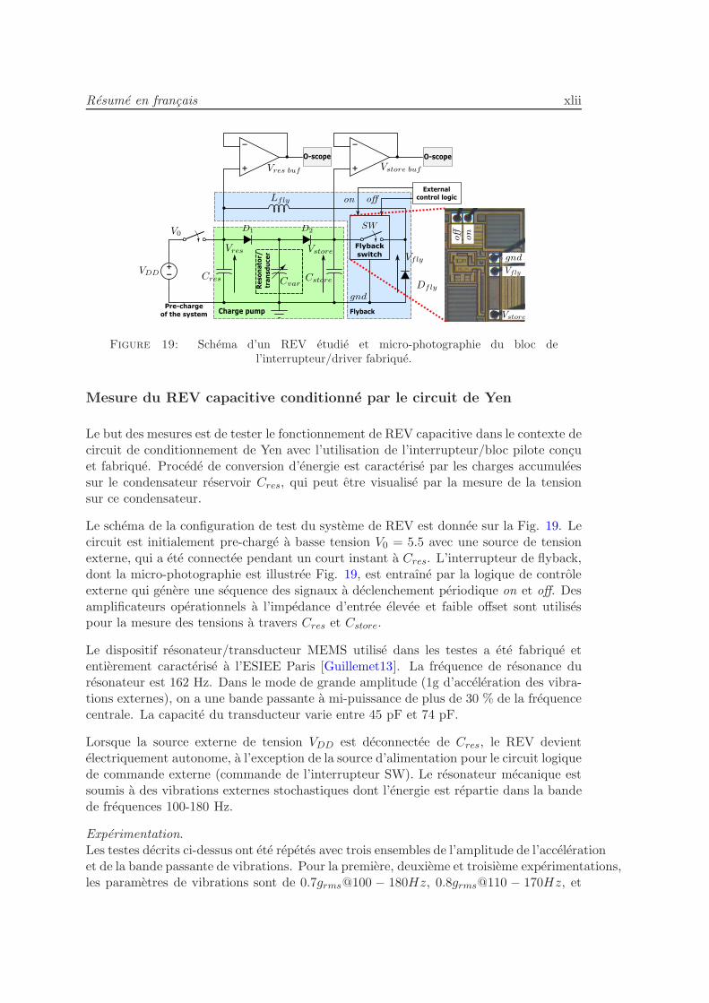
Mesure du REV capacitive conditionne par le circuit de Yen
Le but des mesures est de tester le fonctionnement de REV capacitive dans le contexte decircuit de conditionnement de Yen avec l’utilisation de l’interrupteur/bloc pilote concuet fabrique. Procede de conversion d’energie est caracterise par les charges accumuleessur le condensateur reservoir Cres, qui peut etre visualise par la mesure de la tensionsur ce condensateur.
Le schema de la configuration de test du systeme de REV est donnee sur la Fig. 19. Lecircuit est initialement pre-charge a basse tension V0 = 5.5 avec une source de tensionexterne, qui a ete connectee pendant un court instant a Cres. L’interrupteur de flyback,dont la micro-photographie est illustree Fig. 19, est entraıne par la logique de controleexterne qui genere une sequence des signaux a declenchement periodique on et off. Desamplificateurs operationnels a l’impedance d’entree elevee et faible offset sont utilisespour la mesure des tensions a travers Cres et Cstore.
Le dispositif resonateur/transducteur MEMS utilise dans les testes a ete fabrique etentierement caracterise a l’ESIEE Paris [Guillemet13]. La frequence de resonance duresonateur est 162 Hz. Dans le mode de grande amplitude (1g d’acceleration des vibra-tions externes), on a une bande passante a mi-puissance de plus de 30 % de la frequencecentrale. La capacite du transducteur varie entre 45 pF et 74 pF.
Lorsque la source externe de tension VDD est deconnectee de Cres, le REV devientelectriquement autonome, a l’exception de la source d’alimentation pour le circuit logiquede commande externe (commande de l’interrupteur SW). Le resonateur mecanique estsoumis a des vibrations externes stochastiques dont l’energie est repartie dans la bandede frequences 100-180 Hz.
Experimentation.Les testes decrits ci-dessus ont ete repetes avec trois ensembles de l’amplitude de l’accelerationet de la bande passante de vibrations. Pour la premiere, deuxieme et troisieme experimentations,les parametres de vibrations sont de 0.7grms@100 − 180Hz, 0.8grms@110 − 170Hz, et
Figure 20: Evolution de l’etat du systeme etudie en mode autonome soumis a desvibrations externes stochastiques avec trois stimuli differents. En haut : tension aux
bornes de Cres = 1µF, en bas : energie de Cres.
1grms@90 − 175Hz, respectivement. Tous les trois testes ont demarre avec V0=5.5 V.La frequence d’activation de l’interrupteur a ete fixe a 5 Hz.
Fig. 20 presente l’evolution dans le temps de Vres (graphique du haut) et de l’energie deCres (graphique du bas). Apres 3000-4000 secondes de fonctionnement de systeme au-tonome Vres monte jusqu’a 15-20 volts. Des chutes subites de Vres peuvent etre observees.Cela se produit quand Vres atteint un niveau auquel un ”pull-in” dynamique se produit.Les chutes de Vres sont dues au court-circuit entre les plaques de condensateur variableCvar : quand ca se passe Cres se decharge tres vite a travers la diode D1 jusqu’a momentou la tension au cours de laquelle le pull-in disparaıt. Il s’agit d’un effet indesirable liea la physique du dispositif MEMS presente dans [Guillemet13]. La tension de pull-indynamique depend de l’amplitude de l’acceleration des vibrations externes : a des ampli-tudes d’acceleration inferieurs, la tension de pull-in est plus elevee. En consequence, lesniveaux plus eleves de Vres peuvent etre obtenus a l’amplitude d’acceleration inferieur,comme indique par la mesure. Le court-circuit ”emule” une charge consommant l’energiedu condensateur de stockage, et on peut voir que la production d’energie sur Cres eststable sur l’intervalle de temps observee (4000-7000s).
Au cours de trois testes, la tension maximale Vres produite est de 21 V, 21.5 V et 17 V,ce qui correspond a l’energie sur Cres de 220 µJ, 230 µJ et 145 µJ, respectivement (acomparer avec l’energie initiale de 15 µJ correspondant a Vres = V0=5.5 V). Le taux deconversion d’energie moyenne maximale (puissance) mesure par la pente des segmentsdroits de la courbe d’energie est comprise entre 190 et 750 nW (cf. Fig. 20). Ces chiffresdonnent les valeurs de l’energie nette et la puissance disponible pour l’alimentation dela charge, y compris la consommation de l’interrupteur/driver, ainsi que les pertes dansles elements reactifs et dans les diodes.
Resume en francais xliv
Conclusion et perspectives
La recuperation de l’energie des vibrations est un concept relativement nouveau qui peutetre utilise dans l’alimentation des dispositifs embarques de puissance a micro-echelleavec l’energie des vibrations omnipresentes dans l’environnement. Nos etudes sur lesrecuperateurs d’energie vibratoire (REV) ont contribue au developpement d’une visionmoderne sur tels systemes bases sur le principe de conversion d’energie electrostatique(capacitive). Cette vision se resume en deux mots: ”complexite” et ”non-linearite”. Lacomplexite de l’electronique et de la commande permettent d’obtenir le maximum desperformances d’un transducteur/resonateur; nous considerons que jusqu’a recemment lavoie de la complexite a ete peu exploree par la communaute.
Les travaux sur l’analyse et l’optimisation de circuit de conditionnement pour les REVscapacitives ont abouti le developpement d’un algorithme de conversion d’energie op-timale et adaptatif ; cette etude a ete validee par la modelisation comportementale.Les travaux de conception electronique ont abouti l’implementation d’un algorithmeadaptative au niveau transistors et la realisation et la fabrication d’un des bloc clefs(l’interrupteur/driver haute tension) en technologie CMOS AMS035HV. Enfin, en se ser-vant d’un bloc fabrique, la validation experimentale des resultats obtenus par la theorieet par simulation a ete faite.
Il a ete conclu que la validation experimentale de la theories est compliquee par unemaıtrise insuffisante des parametres des systemes fabriques par les procedes MEMS, cequi fait que les systemes reels sont differents des modeles utilises pour la theorie. Lesmesures precises de la dynamique d’un microsysteme sont egalement problematiques,or la validation rigoureuse de la theorie exige une mesure exacte de la position de lamasse mobile. Ceci est un point que nous envisageons d’aborder dans un futur proche,en cooperation avec le groupe de recherche de Philippe Basset de l’ESIEE Paris.
La plupart des questions sur les REV capacitives restent ouvertes ; les axes de recherchespossible que nous envisageons dans le futur proche sont resumes ci-dessous:– Elargissement de la bande frequentielle des REVs. Cette etude concerne des structuresresonantes exploitant une non-linearite.– Realisation d’un prototype electronique de REV intelligent et adaptatif.– Developpement de l’analyse sophistique des REVs. Cet axe concerne l’explorationtheorique et le developpement de l’analyse des REVs, l’etude des phenomenes dus a lacomplexite et a la non-linearite prenant en compte le couplage mutuel electromecanique.
Chapter 1
Introduction
1.1 Overview
Energy is presented everywhere in the environment surrounding us - available in theform of thermal energy, light (solar) energy, wind energy, mechanical energy and manyothers. Throughout the history people used to derive benefit from different ambientenergy sources so to apply them for their daily needs. Thus appeared windmills andwaterwheels that date back to many hundreds and thousands years. Before the electricityera and before discovering of electrical energy sources (invention of batteries, Volta,1799, dynamo machines, Faraday, 1831), energy harvesting was the only way to getany useful power. Hence, the concept of energy harvesting is not new. Except thatthe methodology and principles of converting energy evolve, as well as the number ofpotential energy sources has been growing up.
Today, the energy harvesting is considered with a new focus: generation of electricalsupply for powering miniature devices, like those used in wearable electronics and wire-less sensor networks. These devices need small amount of energy (up to milliwatts),however, there is a strong requirement on the size and reliability of the supply genera-tion. The energy sources presenting a practical interest for microscale energy harvestingare: mechanical vibrations, thermal gradients, light (solar) and electromagnetic (RF).These energy sources are virtually unlimited and essentially free, if they can be capturedat or near the system location.
This chapter presents a general overview of energy harvesting, including different sourcesand applications of use as well as various conversion techniques presently employed anddocumented in the literature. Furthermore, this chapter discusses reasons and moti-vations for our research in energy harvesting topic, specifically based on a mechanicalvibration energy harvesting. Finally, our contribution to the existing study will besummarized.
1
Chapter 1. Introduction 2
1.2 Thesis outline
Chapter 1 introduces the problem of supply of autonomous systems and discusses thesolution which can be provided by the energy harvesting techniques. The motivation forharvesting the mechanical vibration energy is discussed. The chapter describes differentconversion methods and explains the need of associated conditioning electronics. Thestate of the art of electrostatic harvesting systems is presented and our contribution tothe existing study completes this chapter.
1.3 Concept of energy harvesting
We start this chapter by defining the meaning of ’energy harvesting’. Fundamentally,energy harvesting (also known as power harvesting or energy scavenging) isthe process of capturing energy from one or more of environmental energy sources,accumulating them and storing them for later use. Energy harvesting devices mustefficiently capture, accumulate, store, condition and manage this energy, and supply itin a form compatible with the needs of the electrical load.
1.4 External energy sources and applications
Among numerous energy sources widely used for harvesting today are:
• mechanical kinetic energy (from sources such as vibration, mechanical stressand strain);
• thermal energy (waste energy from furnaces, heaters and friction sources);
• light energy (captured from sunlight or room light via photo sensors, photodiodes or solar panels);
• electromagnetic energy (from ambient RF waves);
• natural energy (from sources such as wind, water flow, ocean currents, andsolar);
• human body (a combination of mechanical and thermal energy naturally gener-ated from bio-organisms or through actions such as walking and sitting);
• other energy (from chemical and biological sources).
All of the above ambient energies are available for the electric energy generation for pow-ering various appliances frommega-watts to nano-watts range, which are summarizedbelow:
Chapter 1. Introduction 3
• Mega-watt applications comprise power supply in residential and industrialdomains. Typical renewable sources suitable for these domains are hydraulic po-tential energy (by using the gravitational force of falling water [Warnick84]), solarenergy (by using photo-voltaic panels [Hamakawa87, Prasad05]) and wind energy(by using wind turbines [Ackermann05]).
• Milli-watt to micro-watt applications involve low power applications suchas calculators powered by solar cells [Roen77] and micro-solar power sensor net-works [Taneja08], vibration powered wrist watches [Starner03], micromachinedthermopiles [Wang07], shoe-mounted piezoelectric generators [Shenck01], vibra-tion electromagnetic [Williams01] and electrostatic generators [Roundy02], etc.
• Nano-watt applications having size between molecular and microscopic dimen-sions are based on emerging nanotechnologies. Examples of energy harvestingin such applications are the piezoelectric nanowires [Gateway], photovoltaic cellsbased on nanometer-scale heterojunctions [Aydil06], carbon nanotubes [Aroudi13],noise harvesters for nanosensors [Neri11], etc.
Present study concerns the micro-watt power applications for the autonomy of the micro-scale devices.
1.4.1 Self-powered microsystems
Advancements in microelectronics technologies have increased power efficiency of mi-crosystems by reducing power consumption requirements. At the same time, theseprogress resulted in growing interest in autonomous microsystems using environmen-tal energy for self-supplying. The ”ideal” applications are the microsized devices formonitoring and sensing operations with a requirement to operate in difficult-to-reachenvironments. Wireless communication ability of such devices allows a deployment ofnumerous distributed sensing nodes simultaneously. For example, such microsensorscan be employed in monitoring environmental conditions like temperature, humidity, airpressure and Earth’s crust fluctuations from remote or inaccessible areas [Barroca13],can diagnose from the inside the state of health of industrial machines (e.g. motors,turbines and pumps), cars and aircrafts [Benedettini09], electromagnetic interferenceshielding [Chung00] and large-scale structures like bridges [Caicedo01]. Furthermore, inbio-medical field, small implantable or wearable devices supervise essential vital func-tions of patients (e.g. intracranial pressure, blood pressure, heartbeats), diagnose andstimulate the functions of inner organs (heart pacemakers, defibrillators, etc.).
All of these examples have a common challenge of maintenance and battery replacementdue to either their large distribution in a network, or microscopic size, or inaccessibility.For these reasons, ideally each microsensor node must be autonomous and self-poweredfrom the environment, so to comply with the requirement of long lifetime.
The block diagram for the core of a typical wireless sensor node (WSN) is shown inFig. 1.1. It is composed of a sensor, an analog-to-digital converter, a signal processingand storage unit, a transmitter and receiver, an antenna, as well as a power supply and
Chapter 1. Introduction 4
Sensor ADCProcessor/
StorageTransceiver/
Receiver
Energy/Power ManagementPower
Supply
Ante
nna
Figure 1.1: Block diagram of a wireless sensor node (WSN).
Curr
ent
(mA
)
-5
0
5
10
15
20
25
-0.05 0.00 0.05 0.10 0.15 0.20 0.25
Time (s)
SLEEP SLEEP SLEEP
SENSING
and
POWER CONTROL
RECEIVE
TRANSMITHarvester output
Figure 1.2: A typical scenario for the power consumption of a sensor node [Vullers09].
a energy/power management circuit. The system energy dissipation is usually domi-nated by sensing and wireless data transmission as shown in Fig 1.2. Fortunately, theseoperations occur rarely or/and periodically in response only to sporadic events or slowlychanging variables like temperature or air pressure. As a result, most of the time thesystem operates in an idle mode consuming a tiny amount of energy (in nW − µWrange), while the duty-cycle of power-hungry sensing and transmitting tasks (of mWorder) last a short part of the entire period. The system’s average power consumptionis, thereby, relatively low, typically of µW order. Even though a smart timing man-agement of high-power functions allows a reduction of the average power consumptionof the node, the problem of attenuation of peak power consumption may exist. Theenergy may be extracted from the environment at slow rates, and therefore at low powerlevel inadequate for high-peak power requirements. Moreover, ambient energy is natu-rally variable and often unpredictable, and might not be always available. This issuecan be overcame by accumulating the harvested energy in a storage element for furthersupplying when needed.
Chapter 1. Introduction 5
Table 1.1: A comparison of energy sources according to [Rabaey00, Roundy03a,Stordeur97, Vullers09, Zelenay04]
15e-6 mW/cm2 (WiFi)Acoustic noise 9.6e-4 mW/cm2 at 100 Db
3e-6 mW/cm2 at 75 DbPassive human- 1.8 mW (shoe inserts)powered systems
1.4.2 Ambient energy for autonomous microsystems
Authors in [Roundy03a, Rabaey00, Vullers09] analyzed the commonly used renewableenergy sources. Most of them are listed in table 1.1. The table shows the comparison ofvarious energy sources by power and energy densities. Values are estimates taken fromliterature, analysis and several experiments. The most suitable energy sources in termsof energy levels, sizes and feasibility of harvesting devices are : solar, thermal gradients,mechanical vibrations, fuel cells and RF.
Solar cells are the most widely used and the most mature energy harvesting technol-ogy based on the principle of photovoltaic effect. A solar cell uses a PN junction forphotovoltaic energy generation. Photons of light hit the depletion zone around the pn+junction and separate electron-hole pairs within the depletion zone so to free carriers.Under the junction built-in electric field, free electrons and holes jump out from thedepletion region so that electrons drift to the n+-side and holes to the p-side of thesemiconductor material. Accumulated at the opposite sides of the semiconductor posi-tive and negative charges develop an open-circuit voltage. If the load is connected acrossthe cell, electrons travel through it from the n+-side to the p-side so to recombine withholes, generating the current that is directly proportional to the light intensity. Micro-scale systems employing thin silicon-based films have a significantly poorer efficiency
Chapter 1. Introduction 6
than macro-scale solar cells [Safa09]. Nevertheless, these microscopic solar cells harvestgreater amounts of energy compared to other conversion energy mechanisms. Photo-voltaic cells are very effective when a sufficient intensity of light is available (150–15000µW/cm2 in the daytime outdoor applications), however their yield slumps when thelight rates are low (e.g. in the nighttime or in different indoors applications where thegenerated power density is 10 µW/cm2 under the best case conditions [Roundy04a]).
Temperature gradients can be converted to electricity by thermoelectric generatorsthat exploits the thermoelectric Seebeck effect. Thermoelectric generators usually con-sist of an n- and p-type thermoelectric materials electrically connected at the hot endsand disconnected at the cold ends, hence constituting a thermocouple [Toriyama01,Egbert07, Yang13]. The temperature difference occurring across a thermocouple resultsin the heat flow and, consequently, the charged carriers transporting from the hot endto the low temperature junctions. Concentration gradients of electrons and holes inthe materials produces an electric field across n- and p-type materials, respectively. Inthis way each base electrode is ionized with an opposite charge and therefore a voltagedifference is established. If connecting a load across each terminal, an electrical cur-rent is thermally induced [Wang08]. Thermoelectric power generators are effective whenlarge thermal gradients are available, since the voltage produced by the generator isproportional to the temperature difference between the two junctions. In microsystems,however, significant temperature differences (greater 10 oC or 10 K) are unexpectedand, as a result, power and voltage levels are relatively small. For instance, maximum15 µW/cm3 can be generated at 10 oC temperature gradient [Stordeur97].
Radio frequency energy is emitted by sources that generate strong electromagneticfields such as wireless radio networks, cellular phone towers and TV signal. Powergenerators linked to a receiving antenna can capture this free flowing energy and convertit into usable electrical energy. RF power generators must operate close to the energysource, otherwise, the captured RF energy and produced voltage levels are extremelylow. For instance, power densities in the range of 0.01-0.1 µW/cm2 are likely when25-100 m away from a GSM base station (for cell phones) [Vullers09]. However, inpractice, it is not guaranteed that in the application of need an RF radiation sourceis situated nearby. Consequently, except specific application context, it is difficult tofind the benefits of RF energy harvesting over other harvesting mechanisms of availableambient energy sources.
Fuel cells convert chemical energy into electrical energy on the same principle as bat-teries. Though conventional batteries employ reactions among metals and electrolyteswhose chemical nature changes over time, the fuel cells actually consume their fuel suchas hydrogen or methanol (a form of alcohol), leaving nothing but an empty reservoir.Fuel cells have high energy density (up to tens times that of lithium-ion batteries) and,hence, they are very attractive for long operation life applications. Fuel cells, on alarge scale, have been recently deployed in numerous applications such as motor vehicles[Ehsani09]. Micro-sized fuel cells can be used in WSNs, in laptop computers and cellphones as for example is planed by Toshiba [Tos]. A challenge with fuel cells is the hightemperature they must work at in order to obtain a high efficiency. For example, thebest reactor in [Holladay02] is capable of 99 % conversion above 320 oC, however, at270 oC conversion is less than 60 %.
Chapter 1. Introduction 7
(a) Car engine at 3000 rpm1(b) car engine at 2000 rpm
(c) staircase with someone going down (d) drill
Figure 1.3: Typical spectrum of ambient vibrations [Boisseau12]
Mechanical vibrations energy available in many environments and applications canbe converted into electrical energy by means of several conversion mechanisms, includingpiezoelectric, electromagnetic and electrostatic, which are discussed in the next section.Table 1.2 gives results of measurements on various vibrations sources summarized in[Roundy03b]. Vibrations are presented in a relatively large spectrum as shown by a fewexamples in Fig. 1.3.
It is difficult to adequately compare ambient energy sources, because they have differentnature, availability rates and potential energy levels. A common thing however is thatall of them are application dependent. Indeed, RF energy harvesting may be possibleonly if a specific source is introduced, hence it is limited by a location. Fuel cellscan not be hermetically sealed that makes them impossible to be used in implantableapplications. The same limitation concerns the light or solar energy, due to the non-availability of the light in implantable applications or in the dark indoor or outdoorapplications. Conversely, temperature variations are ubiquitous in the environment, butoften they are not sufficiently large to generate practically usable voltages and powerin micro-scale applications without placing thermocouple cells in series. Mechanicalvibrations, however, present a more abundant, stable and relatively high energy source ina wide variety of environments and applications, such as automotive, aircraft, buildings,bridges, industrial tools, moving people, etc. Also, vibration energy harvesting has notbeen studied so long and so deep as for example photovoltaic cells, and therefore presentsa big interest for the research. Mainly for these reasons ambient vibrations energy sourcehas been chosen as a contest of our research project.
1Abbreviation rpm - revolutions per minute, is a measure of the frequency of a rotation. It annotatesthe number of turns completed in one minute around a fixed axis.
Chapter 1. Introduction 8
Table 1.2: Summary of several vibrations sources accordingly to [Roundy03b]
Vibration source Peak Acc. Freq.(m/s2) (Hz)
Car engine compartment 12 200Base of 3-axis machine tool 10 70
Door frame just as door closes 3 125Small microwave oven 2.25 121
HVAC vents in office building 0.2-1.5 60Wooden deck with foot traffic 1.3 385
Breadmaker 1.03 121External windows (size 2 ft X 3 ft) next to a busy street 0.7 100
Notebook computer while CD is being read 0.6 75Washing Machine 0.5 109
Second story floor of a wood frame office building 0.2 100Refrigerator 0.1 240
Human motion 0.35 1-10
1.5 Mechanical vibration energy harvesting
Mechanical vibration energy harvesting concept consists in converting the energy of theparasitic ambient mechanical vibrations into the useful electrical energy. The study ofthis concept is a relatively new subject, comparing for example to the harvesting of pho-tovoltaic energy. Scientific research on vibration energy harvesting for WSN applicationsbegan to take of on the edge of the 2000’s with the growth of microelectromechanicalsystems (MEMS).
1.5.1 General system
As reported in numerous studies, harvesting of kinetic energy of external vibrations isachieved in two steps. At first, a part of the mechanical energy is captured by themechanical part of the harvester - the internal movable parts. At a second stage, thecaptured kinetic energy of the movable parts is converted into an electrical form.
A general model of a Vibration Energy Harvester (VEH) is given in Fig. 1.4. Themechanical part is usually a mechanical resonator, which is composed of a proof masscoupled with external vibrations through an elastic link (e.g. spring). In the mechanicaldomain, there are two reference frames: the global inertial frame Oy, in which externalvibrations take place with acceleration aext, and the reference frame Ox related to thevibrating system, in which the harvester is located. The relative motion of the Oxreference frame can be modeled by applying a force −maext to the resonator (m is aresonator’s mass), and then, the Oy reference frame is considered as inertial [Landau76].
Chapter 1. Introduction 9
Load
Electric
energy
buffer
Conditioning
circuit
Electromechanical
transducermassspring
direction of
vibrations
(vibrating frame)
(fixed inertial reference)
damper
Figure 1.4: General structure of a vibration energy harvester
Thanks to the elastic coupling with the vibrating reference frame Ox, the mass movesin this reference system and the resonator accumulates kinetic energy.
To convert the mechanical energy into electrical, an electromechanical transducer shouldapply an electrically-originated damping force on the mass, i.e. it should perform anegative work on the mechanical system purposely reducing its kinetic energy.
The damping force can be created by a magnetic field, an electric field or a strain ona piezoelectric material. Depending on the nature of the damping force there existelectromagnetic, electrostatic and piezoelectric conversion techniques. Each techniqueoffers different benefits and drawbacks as well as technical challenges that determine itsviability and potential for the integration into self-powered microsystems. An associ-ated conditioning circuit manages the electrical energy flow so as to create an electricalcontext for the desired operation of the electromechanical transducer. The architectureof the electronics depends upon the type of transducer. Furthermore, a conditioningcircuit allows an accumulation the maximum of the harvested energy in the reservoirand a regulation of the output power for a load supply.
The design of a VEH requires the optimization of the mechanical part, the transducerand the conditioning electronics so to increase the efficiency of the whole VEH system.To fulfill this requirement, the mechanical resonator must capture as high kinetic energyas possible, the transducer has to convert the energy as efficiently as possible and theassociated electronics to consume as low power as possible. Therefore, the design ofvibration energy harvester is a complex task submitted to many restrictions and, hence,requiring a careful study and analysis of different issues. Vibration energy harvestingis a multidisciplinary topic that joins specialists from different research fields includingmicro-technologies and electronics as well as fundamental sciences such as physics andmathematics.
1.5.2 Mechanical resonator structure
The mass-spring mechanical structures can be either resonant or non-resonant. Theresonant generators are intended for applications where the source amplitude is smallcompared to the possible proof mass displacement and are efficient in specific narrow
Chapter 1. Introduction 10
bands of frequencies. The non-resonant generators, instead, are used in applicationswhere the external vibration power is spread in a large band at low frequencies and wherethe vibration amplitude is large compared to the allowable proof mass displacement, e.g.harvesting the energy from the human body movement for which the vibration spectrumis between 1 Hz to a few tens of Hz [Buren06, Bowers09].
For a given resonant structure, the maximum displacement of the movable part occurswhen the excitation frequency equals its natural frequency. Tiny deviations from thisfrequency point would eventually result in significant reduction in displacement andoutput power. In real practical applications [Roundy03b, Despesse05, Najafi11], ambientvibrations are characterized by a large spectrum of frequencies between a few hertz andseveral hundreds hertz (cf. Fig. 1.3). Moreover, the observed ambient vibrations areusually variable in time. Due to the problem of frequency deviation, linear resonatorswith high quality factors are characterized by a high selectivity of frequencies (i.e. havingvery narrow bands) may fail to perform optimally in real environment and, hence, arenot well suitable for practical applications.
In order to overcome this issue, recently abundant efforts have been devoted by theresearch community to widen the response bandwidth of resonant energy harvesters. Tothis end, the research of more complex coupling mechanisms introducing the mechanicalnon-linearities has been initiated. A number of different solutions have been presentedin the literature. Thus, the resonators can employ the non-linear [Blystad10] or bi-stable springs [Cottone09]. Also a common approach is to use the non-linear double-mass systems [Galchev12]. These techniques allows a frequency conversion: the low-frequency poor quality factor Q resonator excites a high-frequency high Q resonator;the latter is used for the mechanical-to-electrical energy conversion. Another approachesconsist in eventual impact of the mobile mass with a stopper [Soliman08, Guillemet13],employment of stochastic resonance, and others.
Drastically new approach for capturing nonregular low frequencies has been proposedby [Bu12] in his study of the ”liquid” capacitive harvester. This harvester uses flowingliquid rather than conventional resonating structures to induce variable capacitance andit is more suitable for low frequencies (a few hertz) applications. As authors show, up to2.19 mW of power can be produced at 1 Hz by a small-size device (4cm×1.5cm×1mm).
Another non-conventional capacitive harvester reported in [Naruse09] is a non-resonantlow-frequency structure that consists of a mass-spring mechanism with microball bear-ings rolling with the separation gap control. The separated spring and mass manageto vibrate with long-range movement (about 15 mm) at low frequency and keep theseparation gap constant. This concept makes the structure reliable to high mechanicalstress and owing to a long-range movement, the resonator harvest up to 40 µW at verylow vibration frequency and amplitude (2 Hz, 0.4 g).
An expression characterizing the maximum power Pmax that can be extracted from themechanical vibrations at the acceleration amplitude Aext and the angular frequency ω,with a use of a VEH with a mass m, which maximum displacement is limited to Xlim,is shown next:
Pmax =1
2mAextωXlim (1.1)
Chapter 1. Introduction 11
Table 1.3: Summary of several electrostatic MEMS micropower generators highlight-ing the maximal harvested mechanical power Pmax according to Eq. 1.1
Reported in Device dimensions m, g fres, Hz Xlim, µm Pmax, µW
[Roundy02] 1 cm3 0.1 50 250 39[Mitcheson03] − 0.1 30 500 47[Despesse05] 81 mm2 x 0.4 mm 2 50 95 95[Paracha09b] 11 x 6.5 x 0.86 mm3 0.0461 250 50 18.1[Suzuki10] 11.6 x 10.2 mm2 0.1 63 70 13.8
[Guillemet13] 0.042 cm3 0.066 163 46 15.5
This equation gives an absolute limit for the captured mechanical power by the mass-spring resonator independently of the mechanism of electromechanical energy conver-sion [Mitcheson08, Basset09]. Table 1.3 presents the maximum power estimation cal-culated with Eq. 1.1 for several micro-generators submitted to vibration accelerationAext = 10 m/s−2.
Here, fres is the resonance frequency of the mechanical resonator. As can be observed,typical resonator can capture up to several tens microwatts of mechanical power whenoscillating at resonance frequency at 1 g acceleration.
Study and design of the mechanical part of the VEH is out of focus of this thesis. Never-theless, design and optimization of the electrical part of the VEH requires the knowledgeof the mechanical part as well, and vice versa. Indeed, modeling of the complete VEHon system level must take into account the mechanical part. Therefore, a close interac-tion between designers of both mechanical and electrical parts of the system is required.For this reason, we worked in close collaboration with Philippe Basset and his teamfrom ESIEE Paris (ESYCOM laboratory), who are specialized in microelectromechani-cal systems technology and design (MEMS). This team is responsible for the design andfabrication of the mechanical part and electromechanical interface (transducer).
Our study deals with two resonant capacitive VEH devices fabricated in ESIEE Paris[Basset09, Guillemet13], which are intended to operate at frequencies ranging from oneto a few hundreds hertz.
Since almost two years, the team of Philippe Basset, in collaboration with the team ofLuca Gammaitoni (univ. of Perugia, Italy), studies the nonlinear mechanical structuresallowing to widen the vibration bandwidth and capture the colored noise vibrations(under stochastic resonance). Such nonlinear mechanical prototypes have an impact onthe conditioning circuits and analysis methodology of the VEH system. The nonlinearanalysis of electrostatic vibration energy harvesters dynamics in the coupled electrome-chanical mode is investigated by the team of Elena Blokhina from the University CollegeDublin and my supervisor Dimitri Galayko since 2011 [Galayko11a, Blokhina12].
Chapter 1. Introduction 12
1.5.3 Electromechanical energy transducers
1.5.3.1 Methods of electromechanical energy conversion
As we mentioned previously, there exist three basic methods used to convert the energyof mechanical vibrations to electricity, namely electromagnetic (EM), electrostatic (ES)and piezoelectric (PE).
An electromagnetic conversion occurs when a coil moves with relation to an externalmagnetic field, so that there is a variation of magnetic flux crossing the coil section.Typically, the coil is attached to a mobile mass oscillating in the magnetic field createdby a stationary permanent magnet as shown in Fig. 1.5a. The variation of the magneticflux results in inducing an AC voltage on the coil, according to Faraday’s law. Conversely,the same conversion principle is applied to a fixed coil and a moving magnetic mass. Anumber of ED harvesters have been reported in literature, a few to mention: [Williams01,Amirtharajah98, Beeby07, Saha08, Sari10, Cheng07, Kulkarni06, Cao07].
An electrostatic harvester harnesses energy from the work performed by vibrationsagainst the electrostatic force of a vibration-dependent variable capacitor Cvar. En-ergy conversion is achieved as the capacitance of the charged capacitor decreases (thegap between the capacitors plates increases) as shown in Fig. 1.5b. Under chargeconstrained or voltage constrained conditions, the electricity is generated. Both ofthese techniques will be discussed in section 1.7. Numerous charge and voltage con-strained capacitive harvesters have been presented during the last decade as reportedin [Meninger01, Roundy02, Tashiro02, Miyazaki03, Mitcheson04, Torres05, Despesse05,Chiu06, Paracha07, Mitcheson08, Kuehne08, Suzuki10].
A piezoelectric harvester converts mechanical energy by straining a piezoelectric ma-terial. The deformation of a piezoelectric material causes charge separation across it,producing an electric field and, consequently, a voltage drop proportional to the appliedstress. A piezoelectric transducer usually consists of a cantilever beam fixed on one endwhile a moving mass is attached on the opposite side as illustrated in Fig. 1.5c. A beamis built as a two-layer bimorph structure with two piezoelectric sheets separated by adielectric shim. As the mobile mass resonates, one side of a cantilever is in tension andthe other is in compression, creating an AC voltage. Examples of reported piezoelectricgenerators can be found in [Shenck01, Glynne-Jones01, Roundy04b, Ottman02, Jeon05,Marzencki05, Sodano05, Shen08, Defosseux11].
1.5.3.2 Comparison of conversion methods
Each type of transducer presents both advantages and drawbacks depending on theapplication (amplitudes of vibrations, frequencies, etc.). An excellent state of the art ofvarious types of transducers as well as their comparison is provided in a study [Beeby06].A qualitative comparison of these techniques in terms of power densities, operationconditions, integration potential and so on, is summarized in Table 1.4.
Electromagnetic harvesters have a good power density and do not require a complexpower conditioning. However, a fundamental weakness of such transducers is that they
Table 1.4: Comparison characteristics of vibration energy harvesting techniques -electromagnetic (EM), electrostatic (ES) and piezoelectric (PE).
MicrosystemAdvantages Drawbacks Implementation
Challenges
-Robustness -Low output voltage -Difficult integration of bulkymagnet
EM -High output current -Low efficiency at low frequen-
cies and small sizes-Possible need of additionaltransformer
-No initial energy required-Simple concept
-Scalable -Need of energy investment -Possible mechanical instability-CMOS compatible -Complex power conditioning
ES
-High output voltages -High impact of parasitic ca-pacities
-High coupling
-High output voltage andpower
-Power conditioning -Difficult integration of PZTmaterial
PE
-No initial energy required -Voltage rectification -Reduced coupling of of thin-films
-No need to control any gap -Fatigue of PZT beams
are not suitable for miniaturization and are not compatible with CMOS process, becausethey possess high-volume coils and magnets.
Nowadays breakthrough in studying piezoelectric transducers offers a relatively highoutput electrical power yield of order of tens-hundreds micro-watts. Also, the piezo-electric transducer may be integrated on chip with built-in electronics; such a system isknown as ICP ”Integrated Circuit Piezoelectric”. Another positive side of piezoelectrictransducers is that they do not need of extra energy source for starting. However, ahigh piezoelectric harvesting efficiency is often obtained with resonant structures, andis limited to a narrow frequency band. Different nonlinear techniques of frequency up-conversion are also widely used for overcome the limitation imposed by resonating and
Chapter 1. Introduction 14
Load
Electric
energy
buffer
Conditioning
circuit
Electrostatic
transducer (Cvar)massspring
direction of
vibrations
(vibrating frame)
(fixed inertial reference)
damper
Figure 1.6: General structure of an electrostatic vibration energy harvester (e-VEH)
rather high-frequency piezoelectric structures [Kulah08]. These techniques often usepermanent magnets, which adds bulk and cost, and prohibit some class of applications(in particular, the medical embedded self-powered devices). Another serious issue re-lated with piezoelectric transducer concerns the lifetime: since in the energy harvestingapplications the piezolayer strain should be high, there is a risk of material degradation(fatigue, depolarization, micro-”fissure” [Pillatsch13]). Few work have indicated theseissues; further in-depth studies are required to evaluate the reality of this limited lifetimeissue.
Electrostatic transducers commonly employ a silicon micromachined MEMS technology,whose fabrication process is similar to those of a standard CMOS. Therefore, becauseof the process compatibility, it is easier to integrate electrostatic transducers basedon mature MEMS technology than either electromagnetic or piezoelectric converters.Although the power levels offered by electrostatic transducers are not high (max. fewtens of microwatts), and although electrostatic transducers need an initial electricalbiasing, capacitive harvesters are seen as one of the most promising energy generatorsfor future miniaturized autonomous embedded systems. Comparing with piezoelectrictransducers, they don’t have lifetime issues related with piezoelectric transducers, andthey can generate high voltages while having very small size.
1.6 Electrostatic energy harvester
This work deals with electrostatic (or capacitive) transducers. An electrostatic trans-ducer is a capacitor whose plates move relatively to one another. Fig. 1.6 demonstratesthe system of electrostatic vibration energy harvester (e-VEH), in which the capacitivetransducer is used to transfer the mechanical energy to the electrical domain. For that,the mobile mass of the mechanical resonator is associated with a movable electrode thatmakes Cvar vary with the motion of the mass. In other words, the variation of thecapacitance is related with the kinetic energy stored by the moving mass.
As was mentioned before, the electrostatic transducer may be directly implemented onchip together with a conditioning electronics. The miniature silicon-based design ofa variable capacitor is possible owing to the microelectromechanical systems (MEMS)
Chapter 1. Introduction 15
technologies which nowadays are mature, such as deep reactive ion etching (DRIE)[Madou02].
1.6.1 Variable capacitor structures
Capacitive transducer is a two-terminal device. The first terminal is attached to themobile proof-mass. The second electrode is fixed to the vibrating frame linked to the(non-inertial) reference system Ox. Hence the transducer capacitance varies in responseto the motion of the mobile mass in the frame Ox. There exist various types of capacitivetransducers, differing by the geometries and by the law of the capacitance variation.The displacement of the capacitor’s movable plate may occur in plane on the substrate(in the plane parallel to the substrate) or out of plane (in a direction normal to thesubstrate). For both topologies the capacitance may change by varying the gap betweenthe electrodes or by varying the overlap area of the electrodes.
The Out-of-Plane Gap-closing Plate (OPGP) capacitor as well as the In-Plane OverlapPlates (IPOP) capacitor, shown in Fig. 1.7a-b, suffer from the problem of possible con-tact of top and bottom electrodes resulting in an electrode stiction, which could cause thecollapse of the system and destroy the device due to elevated short-circuit currents. Thecapacitor plates for in-plane motion are typically fabricated with interdigitated fingers ina comb structure. An In-Plane Overlap Comb (IPOC) structure (cf. Fig. 1.7c) is able toprovide a greater mobile mass displacements while achieving a higher capacitance varia-tion and minimizing the minimal capacitance, however it suffers from stability problems.Variation of the gap distance in the In-Plane Gap-closing Comb (IPGC) structure (cf.Fig. 1.7d), alternatively, ensures better stability owing to smaller spring deflections andlarger both minimal and maximal capacitance values [Roundy04b].
Regardless on the structure of the MEMS device, the plates of the variable capacitorhave parasitic series resistance and parasitic capacitances between the moving plates,the substrate and sidewalls. The parasitic capacitance set a lower bound on the min-imal transducer capacitance, so reducing the ratio Cmax/Cmin, which determines thetransducer efficiency in the energy conversion process [Roundy03b]. Therefore, engi-neers designing the transducer variable capacitor must take into account these factorsand must found the trade-off between the capacitance variation, minimal capacitanceand parasitic components, as well as the mechanical stability of the structure.
Capacitive transducers can be divided into two categories:
• Electret-free converters, which use conversion cycles made of charging and dis-charging of the capacitor, and therefore requiring an active electronic circuit toapply the charge/discharge cycle on the structure. The electronics must be syn-chronized with the capacitive variation.
• Electret-based converters, which use electrets giving them the ability to directlyconvert mechanical power into electricity.
The electret-free devices are passive structures that require an energy cycle to convertmechanical energy into electricity. Electret-based devices are similar to electret-free
converters, the difference is in an electret level added on one or two plates of the variablecapacitor. The electret creates a variable polarization of the electrode, so generating acurrent providing electrical power for the load. So, such devices enable straightforwardmechanical-to-electrical conversion. This PhD study project is focused on electret-freeconverters for several reasons, mainly because such a category is more interesting interms of research. An extensive review of the state of the art of electrostatic VEHsdevices was presented in PhD thesis of R. Guillemet [Guillemet12].
1.6.2 Conversion principle of electret-free structure
For the simplicity, consider a simple rectangular parallel plate capacitor, given by Cvar =ε0S/d, where ε0 is the dielectric constant, S - the overlap area of the plates, d - thegap distance between the plates. Depending on structure of the capacitive transducerdemonstrated in previous subsection, the decrease of the capacitance can occur eitherby increasing d, or by reducing S. For example, in the case when the capacitance variesdue to the change of the gap distance between the plates (d = d0 ± x)), the minimumand maximum of the capacitance depends on the amplitude of the displacement of theelectrodes:
Cmax,min = εS
d0 −X0 ±X1
, (1.2)
where X0 is an eventual average position of the mobile mass, X1 is the amplitude of themobile mass displacement, d0 is the initial gap of the transducer, at zero displacement.Parameters X0 and X1 depend on the parameters of external vibrations (amplitude andfrequency), which in turn are subjected to variations.
As we mentioned, electret-free converters require a specific charge-discharge cycle. Var-ious types of cycles enable the energy conversion with a capacitive transducer, but themost commonly-used are charge- and voltage-constrained cycles as shown in Fig. 1.8.They both start when the capacitance is maximal (point A). At this point, a charge Q0
is injected into the capacitor polarizing it thanks to an external source.
Chapter 1. Introduction 17
(a) (b)
Figure 1.8: QV-cycles of electromechanical energy conversion: (a) charge constrainedand (b) voltage constrained.
In case of the charge constrained cycle, the energy conversion is initiated as the capac-itance decreases so that it remains charged with the same amount of charges Q0 (Fig.1.8a). As Cvar decreases, voltage across it increases so to satisfy Q = CV . When Cvar
reaches the minimal value and the voltage becomes maximum Vmax (point B), the fullcharge is returned to the reservoir capacitor until the voltage across capacitance becomeszero (point C). The following cycle starts when the the capacitance is pre-charged againwith Q0 to the initial voltage V0. The converted energy is equal to the surface area ofthe triangular that can be numerically expressed as:
∆WQ const =1
2(Cmax −Cmin)V0Vmax =
=1
2V 2max
Cmin
Cmax(Cmax − Cmin) =
1
2V 20 Cmax(
Cmax
Cmin− 1)
(1.3)
In case of the voltage constrained cycle, the energy conversion also starts at the maximumcapacitance value (point A in Fig. 1.8b). At this point, the transducer is electricallyconnected to a constant voltage source Vvc. Since the voltage Vvc is kept constant andthe capacitance decreases, the charge decreases as well, so generating the current whichrecharge the voltage source with the energy converted from the mechanical domain.When the capacitance reaches its minimum (point B), the remaining charge Qmin iscompletely collected and stored (point C). The following cycle starts when the capaci-tance is again maximum, and so on. The amount of energy converted at each cycle alsocorresponds to the area of the triangular:
∆WV const =1
2(Cmax −Cmin)V
2vc =
1
2(Cmax
Cmin− 1)CminV
2vc (1.4)
The comparison of the voltage constraint and the charge constraint cycles can be doneif some hypotheses about the available voltage sources are made. If for two schemesthe same constant voltage source is available, so that V0 = Vvc, obviously the chargeconstrained cycle provides Cmax/Cmin times more energy. By contrast, is the maximalvoltage is equally limited in the both schemes, for example, for technological limits,Vmax = Vvc and the voltage constrained cycle provides Cmax/Cmin times more energy.
Chapter 1. Introduction 18
Precise implementation of the both cycles is difficult, because of the need of precisesynchronization between the charge flow on the transducer and the transducer capacityvariations. The conditioning circuits implementing such a variable biasing are discussedin the next section.
1.7 Energy interface conditioning circuits
1.7.1 Needs for energy conditioning
Conditioning electronic circuits are the key elements in energy harvesting systems sincethey determine the efficiency of the electrical energy generation from the ambient energy,whatever the energy source is. Their role is to assist the energy conversion process andto provide a stable constant DC voltage for the load supply. According to this role,the conditioning circuits are usually divided in two functional parts: interface for thetransducer conditioning assisting the energy conversion process and the load interfacetogether with the power management blocks.
Depending on a type of the transducer, functions and topologies of the transducerinterface are different. Thus, electromagnetic generators use relatively simple inter-face circuits achieving a rectification and regulation of a considerably low AC voltage[Beeby07, Rao13]. Piezoelectric generators require the interface circuits for the similarreasons: rectification the generated AC voltage and its regulation according to the loadspecifications [Sodano04, Lefeuvre06, Miller12]. Note that the voltage amplitude pro-duced by a piezoelectric generator depends on several factors such as the mechanicalvibration parameters, characteristics of the piezoelectric element and its dimensions,etc. Therefore, the output voltage must be either increased, or reduced. Electrostatictransducers, in turn, require the adaptation interface circuits to control the charging anddischarging events of the transducer capacitance and to manage the converted energy inthe optimal way [Mur-Miranda04, Torres06, Mitcheson10].
The power management interfaces are used to merge the energy converted from differentsources [Christmann10] and to adapt it to the load needs using switched mode dc-dcconverters. For the optimum load resistance matching, typically buck [Kim07], boost[Paing08], buck-boost [Kong10] and flyback [Kasyap02] switching converter topologiesare employed. Also, a self-adjustable topology can be used based on charge pump[Maurath08].
Studies [Sodano04, Szarka12] provide a literature review of power conditioning circuitsfor VEHs, grouping different concepts according to functionality, complexity and effi-ciency. Although this review examines the circuits assisting only the piezoelectric andelectromagnetic transducers (i.e. focusing on various rectification techniques and voltagestep-up/down converters), it also states on existing solutions of general issues inherentto all types of generators: start-up, optimum load resistance matching and power man-agement techniques.
As can be seen, designing of conditioning electronics for the VEH is a complex taskthat requires a wide knowledge in analog and power electronics, but also knowledge in
Chapter 1. Introduction 19
transducers and storage elements. Furthermore, the conditioning circuits are subjectedto several strict limitations as discussed in the following section.
1.7.2 Requirements for conditioning electronics
Taking into account the unpredictability of ambient vibrations and usually the lowlevels of available energy, conditioning circuits should have adaptive and self-startingproperties. Indeed, if for example, the ambient energy is temporarily very low so thatthe harvester consumes more than it converts, it is desired to turn the harvester intothe idle mode for this period. Otherwise, it would consume all the accumulated energyincluding the energy needed for a start-up. Therefore, at microscale, power conditioningelectronics design requires trade-offs different from those for high power applications,where the power overhead of the control electronics is less significant.
The size and volume of the overall system should be minimized, as the VEH will be usedin embedded applications. Therefore, the conditioning circuits of the final VEH systemsshould integrate as much blocks as possible on a single chip.
1.7.3 State of the art of conditioning circuits for e-VEH
The interest of the community in designing the conditioning electronics for the capacitivetransducers started to grow in the beginning of 2000th with the development of matureMEMS technologies and progress in CMOS technologies that shrank enough in sizeand power. The following subsections present the reported conditioning circuits for thecapacitive transducers that we have examined in order to select one as a base of ourresearch.
1.7.3.1 Primitive continuous conditioning circuit
The primitive circuit consists of a large pre-charged reservoir capacitor Cres, a muchsmaller transducer variable capacitor Cvar and a load resistance (Fig. 1.9, [Basset09]).When Cvar varies, the charge flux occurs between Cres and Cvar, and its intensity de-pends on the resistance value. The current through resistance dissipates energy, whichin turn is replenished by the mechanical energy extracted by the variation of Cvar.
The functioning of this circuit is based on the hypothesis that the sum of charges of Cres
and Cvar is constant in time. In other words, we suppose that that there is no leakageon these capacitors, that is obviously not realistic. Hence, this circuit does not presentthe application interest.
Two secondary drawbacks of the circuit are the following. First, this circuit is unable toincrease the the pre-charge voltage of Cres. It is known that capacitive transducers oftenneed high polarization voltages to be efficient (tens of volts), while the initially availablevoltages are usually low (a few volts). This architecture does not contain the mechanismallowing augmentation of the polarization voltage from a low initial level. The seconddrawback is the AC voltage supplying the load. By consequence, a rectification is needed.
Nevertheless, this circuit can be useful in laboratory tests, for example in characteriza-tion of the fabricated transducers. Thus, Cres can be replaced by a DC voltage source.Such a technique has been used for measuring the capacitance of the transducer devicefabricated in ESIEE Paris (cf. section 4.5.1).
1.7.3.2 Charge constrained circuit
In the charge constrained circuit shown in Fig. 1.10a, a transducer capacitor Cvar ischarged from the pre-charged Cres to some initial voltage V0 when Cvar capacitance ismaximal. The energy transfer uses an inductor as an intermediate energy buffer andtwo switches. The time for energy transfer is negligible with respect to a Cvar variationcycle. Then, two switches are open and Cvar decreases keeping the charge constant (cf.the QV-diagram in Fig. 1.8a). When Cvar is minimal, the conditioning circuit providesan inverse charge flow (and energy) from Cvar to Cres.
This circuit requires a precise gate clocking of the switches SW1 and SW2; in fact duringone cycle, switches are commutated two times each at exact moments (at Cvar=Cmax
and Cvar=Cmin).
This circuit and its slight modifications are the best studied by the e-VEH designerscommunity. To our knowledge, there exist two complete realizations of it. The oldest
Chapter 1. Introduction 21
one is realized in MIT in 2001 by S. Meninger [Meninger01]. Another one, implementedwith a transformer rather than inductance, is realized by Despesse et al. [Despesse05].
1.7.3.3 Voltage constrained circuit
A simple voltage constrained circuit [Torres06] is shown in Fig. 1.10b. The systememploys the battery instead of capacitor Cres; this allows recharge the battery Theoperation of the circuit is described by the QV-diagram in Fig. 1.8b. During the pre-charge condition, SW2 and SW5 are switched on to store energy in the inductor L.Switches SW3 and SW4 are turned on by simultaneously turning off SW2 and SW5to charge Cvar. The unidirectional switch SW1 is turned on to allow the current toflow from Cvar to the battery. When the variable capacitor has reached its minimumvalue, SW1 is turned off. In order to completely recover the charge across the variablecapacitor, reverse switching sequence of the pre-charge condition is used.
The physical IC realization of this circuit including the control of the switches has beenpresented in [Torres10].
1.7.3.4 Charge pump circuit
The charge pump employment in energy conditioning circuit was initially proposed byS. Roundy [Roundy02]. This solution eliminates the problem of the control of the chargeflow onto and from the variable capacitor. The switches are replaced by the diodes thatallow a uni-directional charge flow.
When Cvar is at Cmax, diode D1 is on, and charges are transferred from Cres to Cvar.When the capacitance decreases, both diodes are blocked. Since Cvar is electricallyisolated, its charge is constant and the decrease of the capacitance results in the increaseof its voltage. When Cvar is at Cmin, diode D2 is forward biased and the ”energized”charges from Cvar are ”pumped” to a small storage capacitor Cstore, which is largerthan Cvar but much smaller than Cres. The mechanical vibrations have done a workon the transducer capacitor causing an increase in the total energy stored in the systemthat corresponds to the increase of the voltage on Cstore with respect to Cres. A moredetailed description of the charge pump will be given in section 2.3.
After several charge pump cycles the storage capacitor eventually saturates that meansthat it can not receive charges from Cres. Subsequently, some method of returning aportion of the charge from Cstore to Cres should be employed.
1.7.3.5 Charge pump with resistive return
This is the simplest return circuit which can be implemented: a load resistance is con-nected between Cres and Cstore (cf. Fig. 1.12a). In this way, there are two flows ofcharges: one from Cres to Cstore pushed by the charge pump, and another in the oppo-site direction through the resistance pushed by the potential difference Vstore − Vres.
Chapter 1. Introduction 22
Figure 1.11: Charge pump with automatic switches (diodes) used for electromechan-ical energy conversion [Roundy02].
(a) (b)
Figure 1.12: Charge pump with a return circuit: (a) resistive; (b) inductive flyback[Yen06].
A rigorous analysis of this circuit is difficult: since there is a continuous charge cur-rent between Vres and Vstore, and the diodes make the circuit time variable, the exactmathematical model is rather complex.
However, the following hypothesis provides analytical results in good agreement withthe simulation and the experiment. In particular, it allows a prediction of the level ofthe steady-state average value of Vstore voltage and on the converted energy given theparameters of the circuit. Also, the value of resistance providing the maximal powerconversion can be found.
We can consider that the charge pump and the resistance act independently on thecapacitive network CresCstore. It means that the two charge flows can be consideredindependently, and the steady-state circuit operation is obtained when the two chargeflows are equal. Equivalently, instead of the charge flow, the energy flow can be con-sidered: the energy produced by the charge pump is equal to the energy dissipated bythe load resistance. It is reasonable to suppose that under such conditions, Vstore isapproximately constant in the steady state operation.
The calculation of the parameters of the circuit operation can be done with a very simplerelation between the resistance value, the average steady-state value of the voltage Vstore
and the energy ∆W (Vstore) converted in one cycle by a stand alone charge pump with
Chapter 1. Introduction 23
the Cstore capacitor charged to Vstore:
∆W (Vstore) =(Vstore ss − Vres)
2
RLT, (1.5)
where T is the duration of a vibration cycle (period).
The optimal value of the load resistance can be obtained as a left side of the last equationequals to ∆Wmax calculated for the a stand-alone charge pump:
Ropt =(Vstore opt − Vres)
2
∆WmaxT (1.6)
where Vstore opt is the optimal Cstore voltage at which the charge pump converts themaximal energy.
The calculation of ∆Wmax, ∆W (Vstore) and Vstore opt for a stand-alone charge pump willbe done in the following chapters.
Although such a conditioning circuit is very simple, it has several drawbacks:
• The load is not connected to the ground,
• If the ratio Cmax/Cmin is high, the load voltage can be high. Also, the load voltagedepends strongly on the operation conditions of the circuit, and is not stable.
• The energy can’t be accumulated during the circuit operation, and hence the pre-charge of Cres can’t be increased.
• In presence of leakage on the capacitors, the system looses electrical charges andbecomes inactive. Since there is always leakage in real system, such a conditioningcircuit is not suitable for real applications.
In this way, a resistive return circuit is only suitable for laboratory experiments for thecharacterization and study of the charge pumps. In particular, this circuit was used inworks [Florentino11, Guillemet13].
1.7.3.6 Charge pump with inductive flyback return
The return circuit proposed in MIT in 2006 by Yen [Yen06] is based on an inductiveBUCK DC-DC converter topology (cf. 1.12b). The detailed description of this circuitis given in section 2.4.
The flyback return has several advantages.
• Accumulation of the converted energy. As the load is not connected, the convertedenergy is accumulated on Cres. This makes possible an increase of the voltage Vres
while starting at low pre-charge level.
Chapter 1. Introduction 24
• Unique swicth operating rarely and not requiring the synchronization with Cvar.The switch turns on once per many charge pump cycles. Therefore, the control ofthe switch will be performed at significantly reduced frequencies relatively to thecircuit of Fig. 1.10 [Meninger01, Torres10].
• The commutation of the switch will be done in a function of the voltage on Cstore.It is much easier to control the voltage, rather than the capacitance value or amechanical quantity.
For these reasons, we have chosen the Yen circuit as a base of our theoretical study andpractical design of the e-VEH with an intelligent control.
1.7.4 Discussion
We presented a summarized review of the basic conditioning circuits used for capaci-tive harvesters. For practical realization we chosen the charge pump circuit with theflyback return, since it has the advantage of potentially reduced complexity and powerconsumption and it allows a high voltage operation enabling the high converted energy.This circuit, in our opinion, is one of the best candidates for future designs when theoperation voltage limitations of MEMS devices and CMOS technologies will reduce. Asshows our work, this circuit is also compatible with stochastic input vibrations (cf. sec.4.5.2.5).
Mitcheson et al. [Mitcheson12] reported on the effectiveness of the charge- and voltage-constrained electrostatic VEHs when coupled with interface circuits. It was concludedthat the voltage constrained circuits promise higher efficiency than the charge-constrainedcircuits (80 % against 30 % of the maximal efficiency). The study uses the models of thepower MOSFET devices (Vishay PowerPAK). However, this study does not take intoaccount the energy necessary for the control of the circuit, whose complexity risks to begreater than for its charge-constrained counterpart. This can considerably reduce thehigh efficiency.
Several studies concerning the adaptive behavior of conditioning circuit have been pub-lished. Particularly, the work [Kempitiya13] reports on a complete system of the e-VEHincluding a capacitive transducer (of macroscopic size) and an integrated circuit in AMI0.7 µm high-voltage technology realizing an intelligent energy conditioning of the Yenarchitecture. It was demonstrated a net power of 1 µW generated at the load at avibration frequency 98 Hz.
1.8 Conclusion and our contribution
In this chapter we introduced the energy harvesting concept, the ambient energy sourcesand typical applications for energy harvesting. We also presented the harvesting princi-ples of kinetic energy of ambient vibrations, focusing on the existing energy conversionmethods using capacitive transducers. Finally, we discussed the needs of the converted
Chapter 1. Introduction 25
energy conditioning and presented the state of the art study of the interface conditioningcircuits assisting the capacitive converters.
This thesis is a part of the research project ANR SESAM, regrouping four partners(LIP6, ESIEE Paris, TIMA2 and CEA-LETI). The objective of this project is the de-velopment of an ambient energy harvesting and power management microsystem thatmust be adaptive, reconfigurable and robust. This impose to use multiple energy sourcestaking into account the fluctuations of the environment and availability of the energy.The technical problem addressed by this project is the optimization in terms of real timeof the harvesting, utilization and storage of the energy in function of the energy needsof the application and the energy available in the harvesting system. Hence, the projectconsists in designing of the heterogeneous system composed of:- several sources of energy of different nature (vibrations, thermal, photovoltaic, recharge-able battery) captured and converted by different harvesters,- electrical power management unit, which merges all energy converted from differentsources and distributes this energy between the load and battery.ESIEE Paris is responsible for the development of the vibration energy harvesting mech-anism by means of electrostatic (capacitive) transducer using the MEMS technology.LIP6 investigates in the design of the power interface electronics assisting the MEMStransducer; this PhD project is an essential part of the LIP6 contribution to the project.TIMA contributes to the development of the piezoelectric vibration energy harvester.CEA-LETI develops the power management electronics and the intelligent integratedinterface with the load.
This PhD contributes to the existing body of knowledge on Electrostatic-based VibrationEnergy Harvesting (e-VEH) system design. Particularly, this work investigates the low-power high-voltage (HV) design of a e-VEH conditioning electronics in a standard HVCMOS process.
Specifically, this thesis manuscript reports on the following:
• Presents a system-level heterogeneous model of a full e-VEH system allowing a sim-ulation and analysis of the operating conditions of the electrostatic transducer, aswell as a choice of specifications for the design of the power processing electronics.
• Develops a new auto-calibration algorithm allowing the e-VEH system to be adap-tive in presence of non-stable and non-predictable source of external vibrations.
• Provides a new architecture of ultra-low power level shifter driving the high-voltagePMOS switch connect high-voltage floating nodes.
• Proposes a mixed-signal circuit design of the conditioning electronics implementingthe auto-adaptive feature.
• Implements on chip and characterizes by a couple of measurements a driver of ahigh-voltage floating power switch.
2Techniques de l’Informatique et de la Microelectronique pour l’Achitecture des systemes integres
Chapter 1. Introduction 26
• Laboratory tests of the electromechanical energy conversion by means of theMEMS capacitive transducer3 operating within the conventional Yen’s condition-ing circuit, which includes the fabricated in this work integrated high-voltageswitch.
Academic contribution of this thesis consists in several international workshops, nationalconferences and one journal article.
3Designed and fabricated by our project partners - ESIEE Paris
Chapter 2
Study, optimization and modelingof electrostatic vibration energyharvesting system
2.1 Overview
This chapter states on the study and modeling of the electrostatic vibration energyharvesting system. Particularly, we investigate the conditioning electronics assisting thecapacitive transducer, while the research on the MEMS transducer device is carried outin parallel with this work by our research project partners in ESIEE Paris. Thoughour work does not cover the study and design of the MEMS generator, we take intoconsideration all specifications and limitations provided by ESIEE in order to modeland analyze the whole system.
Present study concerns an analysis, optimization and modeling strategy of the VEH sys-tem. First, we introduce in details the architecture and the principle of operation of thechosen conditioning circuit. Thereafter we present the principle factors and conditionslimiting the power generation, and propose a solution of optimization of the VEH oper-ation in order to maximize its energy conversion efficiency. Then we address a problemand propose a solution of the adaptability of the harvester to the occasional fluctuationsin the environment. We also show how to interface the output load with the harvestingcircuit. At the end we show the behavior modeling of the system and discuss simulationresults.
2.2 Auto-synchronous conditioning circuit
As we presented in section 1.7.3, there exist various types of conditioning circuits achiev-ing energy conversion with capacitive transducer. Our study is based on a charge pumpcircuit proposed by Roundy [Roundy02]) and on an inductive flyback return circuit. Thisarchitecture was firstly implemented by B.C. Yen and J.H. Lang in 2006 [Yen06]. Recall
27
Chapter 2. Study, optimization and modeling of electrostatic vibration energyharvesting system 28
Flyback circuitry
ReservoirCharge
pump
Temporary
storage
Load
Output
power
processing
Energy harvesting circuit
Load
interface
Figure 2.1: Block diagram of an electrostatic vibration energy harvester assisted bya ’charge pump and flyback’ conditioning circuit [Yen06].
that the charge pump uses diodes to synchronize the charging and discharging events ofthe variable capacitor, instead of the switches controlled by the precise electronic circuit[Meninger01, Torres10]. Hence, we call the charge pump based conditioning circuit asauto-synchronous.
The operation of the Yen circuit (Fig. 2.2) can be explained with a functional diagramin Fig. 2.1. The charge pump converts kinetic energy of vibrations into electric energyby moving electrical charges from a large reservoir capacitor Cres into a much smallertemporary storage capacitor Cstore. The energy of a charge q stored on a capacitor isinversely proportional to the capacitance:
w =q2
2C. (2.1)
Hence, during the pumping, the energy of the charge increases, and by consequence,the charge pump operation requires additional energy. This energy can only come fromthe variations of the transducer capacitance, i.e. from the mechanical domain. In thisway, the energy accumulated by the capacitive network CresCstore increases, and thegained energy is the energy converted from vibrations plus the initial energy stored inthe capacitors before the operation.
The flyback return circuit used in Yen circuit transfers the energy accumulated in thenetwork CresCstore into the reservoir capacitance Cres. This step has two objectives:
– The converted energy is available on a reservoir capacitance Cres, and can easily beused for different purposes, including the load. Moreover, as it will be shown below, theconverted energy depends on the voltage of Cres, so the Yen flyback circuit provides acontrol on this voltage.
– The charge pump is kept in an electrical state at which a continuous energy productionis possible (cf. explanation in the next subsections).
This conditioning circuit has several advantages, in particular:
Chapter 2. Study, optimization and modeling of electrostatic vibration energyharvesting system 29
Figure 2.2: Schema of the VEH system employing the auto-synchronous conditioningcircuit with an inductive flyback return, proposed by Yen and Lang [Yen06].
• self-powering: as we said, it is possible to accumulate the converted energy in thereservoir capacitor. In this way, the operation voltage of the conditioning circuitcan be increased and the power conversion optimized. This is particularly usefulif only low voltage is available for the system start-up.
• charging and discharging of the variable capacitor occurs automatically by passiveswitches (diodes), hence precise sensing and control electronics isn’t required.
• only one switch is to be controlled: as it will be seen, this switch is synchronizedwith the voltage on Cstore capacitance, which varies much slowly than the variablecapacitance.
In spite of these positive points, this circuit has been poorly studied by the community, incomparison with another types of circuits. The realization of this circuit is difficult sinceit requires an implementation of a non-referenced to ground high voltage switch with lowpower constraints (Sw in Fig. 2.2). However, the progress in the CMOS technologiesmakes this task realistic, and the goal of our work is to proof the feasibility of that.This circuit was first published in 2006, and this PhD project started at 2008. Sincethen, several teams worked on this circuit, in particular, A. Kempitiya from RensselaerPolytechnic Institute [Kempitiya10, Kempitiya12, Kempitiya13]: that proofs the interestof the community to this architecture.
In this section we will present the analysis of the conditioning circuit, explain the dif-ficulties related with its design, modeling and implementation. We will then presentthe modeling techniques we used to study this circuit. We will also present our ideasabout the intelligence which can be added to this circuit so to make it adaptive to theenvironment conditions. These ideas constitute the basis of the original work of thepresent thesis.
Chapter 2. Study, optimization and modeling of electrostatic vibration energyharvesting system 30
2.3 Charge pump
2.3.1 Structure and operation principle
The idea of using a charge pump for electromechanical energy conversion with a variablecapacitor was proposed by Roundy [Roundy02]. A charge pump consists of two diodesand three capacitors: a large reservoir capacitor Cres, a temporary storage capacitorCstore of a smaller size, and a variable capacitor Cvar varying between Cmin and Cmax.The values of these capacitances are related as:
Cres >> Cstore >> Cmax > Cmin (2.2)
The charge pump synchronizes the charge/discharge of the variable capacitor with thevariation of its value without requiring external command. This is its main advantagein comparison with constant-charge/constant-voltage conditioning circuits [Meninger01,Torres09]. The synchronization of the charge flow with the variation of the capacitanceis ensured by diodes D1 and D2. As follows from the topology of the network, the chargecan be transferred in a unique direction: from Cres toward Cvar , and from Cvar towardCstore.
During the analysis of the charge pump, a hypothesis should be made about the diodesmodel. To provide a rough understanding of the circuit operation, however, it is enoughto represent diodes as ideal unidirectional switches:
Id = 0, if Vd < 0,Vd = 0, if Id < 0.
(2.3)
A more accurate model is obtained if a non-zero threshold Vt is assumed:
Id = 0, if Vd ≤ Vt,Vd = Vt, if Id < 0.
(2.4)
Although these models are well-suitable for qualitative and analytical circuit analysis,they are not compatible with a numeric modeling of the system. More information aboutthe diodes numeric modeling will be provided in Section 2.3.4. Here, the diodes will beconsidered as in the model (2.3), unless otherwise isn’t specified.
The mobile electrode of the transducer is supposed to be in a steady-state periodicmotion, and the transducer capacitance varies periodically with a fixed amplitude (sinceCvar is a function of x). The exact law of the transducer capacitance variation is notimportant for the analysis presented in this section; it depends on the displacement lawx(t) and on the displacement-to-capacitance characteristic Cvar(x) of the transducer.However we suppose that over a variation period the transducer capacity experiencesonly one local maximum and one local minimum (Cmax and Cmin).
It is important to understand that the hypothesis of a fixed amplitude of the mobilemass vibration means that the force generated by the transducer does not affect thedynamic of motion of the mobile transducer electrode. This hypothesis is not physical:
Chapter 2. Study, optimization and modeling of electrostatic vibration energyharvesting system 31
as it will be shown, it implies a possibility to convert energy with infinite rate. It isuseful however for analysis purpose. It allows an isolation of phenomena related withtransducer/conditioning circuit operation, and makes an abstraction from mechanicalpart of the system.
The initial state of the charge pump is defined as follows: all three capacitors are pre-charged to a voltage V0, so that Vres = Vvar = Vstore = V0, and the transducer variablecapacitor containing a charge Q0 starts vary from its maximum possible value Cmax. Asall the node voltages are equal, diodes D1 and D2 are both off. An exact knowledge ofthe initial state is only important for the analysis, but not for the system operation.
In practice, this initial condition can be achieved on a circuit with all capacitancesdischarged by charging Cres to a voltage V0 at the moment when Cvar = Cmax. Throughthe diodes, this capacitance shares instantaneously its charge with Cvar and Cstore, soequalizing the voltages. The alteration of the voltage on Cres due to this charge sharingis negligible, since Cres is supposed to be very large.
2.3.2 Energy and charge of the system
In this subsection we show how the energy of the charge pump can be expressed so tomake easier and more elegant the analysis of the circuit.
It can be seen that at the initial state, the energy W0 of the system is
W0 =1
2V 20 (Cres +Cmax + Cstore), (2.5)
and the total electrical charge Q0 of the system:
Q0 = V0(Cres + Cmax + Cstore). (2.6)
The only dynamic process happening in the system is related with the variation of thevariable capacitance. Obviously, the total electrical charge Q of the system is constantin time, equal to Q0, and is the invariant quantity of the system. In contrast, the energyw of the system can change in time if the charge distributes over the capacitances.
In the analysis presented below, when considering the total charge and energy of thesystem, we neglect the the variable capacitance Cvar since it is much smaller than Cres
and Cstore. Under this hypothesis, we can define the system energy as w
w =1
2CresV
2res +
1
2CstoreV
2store =
1
2
Q2res
Cres+
1
2
Q2store
Cstore, (2.7)
where Qres and Qstore are instantaneous charges of the corresponding capacitances.Since the sum of these charges is always equal to Q0, we can introduce the chargevariation ∆Q with relation to the initial charges on these capacitances, Qres0 and Qstore0:
Chapter 2. Study, optimization and modeling of electrostatic vibration energyharvesting system 32
w =1
2
(Qres0 +∆Q)2
Cres+
1
2
(Qstore0 −∆Q)2
Cstore=
= W0 +1
2
∆Q2
Cres+
1
2
∆Q2
Cstore+
1
2
Qres0∆Q
Cres−
1
2
Qstore0∆Q
Cstore.
(2.8)
The last two terms are equal since Qres0/Cres = Qstore0/Cstore = V0, and we have:
w = W0 +W = W0 +1
2
(
1
Cres+
1
Cstore
)
∆Q2. (2.9)
The second term of the expression (2.9)
W =1
2
(
1
Cres+
1
Cstore
)
∆Q2 (2.10)
represents the energy gained by the system because of transfer of the charge ∆Q fromCres to Cstore. This term is nothing else that the energy of a capacitance composed froma series connection of Cstore and Cres charged to ∆Q. This gained energy can also beexpressed through the voltage on this composed capacitor Vres − Vstore:
W =1
2
(Vstore − Vres)2
1
Cres+
1
Cstore
(2.11)
Since Cres >> Cstore and Vres does not change much comparing to Vstore, we can ap-proximate this expression by:
W =1
2Cstore(Vstore − V0)
2 (2.12)
In this way, we can see that the energy of the system increases from the level W0 by aquantity W depending only on the variation of the Cstore voltage equal to
∆Vstore = Vstore − V0. (2.13)
The energy W0 can be taken for a zero energy level of the charge pump, and W canbe considered as the energy converted into the electrical domain by the variation of thetransducer capacitance.
2.3.2.1 Operation over a harvesting cycle
The first cycle starts from the initial state, at which the transducer capacitance Cvar isat its maximal value. During the first half of cycle, Cvar decreases: In order to satisfyQ = CV , the voltage Vvar tends to increase, but in this case the diode D2 turns on, andthe capacitors Cvar and Cstore are connected in parallel. This results in charge sharing
Chapter 2. Study, optimization and modeling of electrostatic vibration energyharvesting system 33
(a) First half of cycle (b) Second half of cycle
Figure 2.3: Equivalent circuit diagram of a charge pump harvesting cycle.
between Cvar and Cstore: since Cvar decreases, charges are flowing from Cvar to Cstore
until Vvar=Vstore as shown in Fig. 2.3a.
The second half of the first cycle starts when vibrations change direction so that Cvar
increases from Cmin to Cmax. As the charge can not flow from Cstore to Cvar because ofthe diodeD2, the charge of Cvar remains constant and Vvar decreases, thereby turning offD2. As Vvar drops further until Vvar=V0, D1 turns on resulting in charge replenishmentfrom Cres to Cvar as shown in Fig. 2.3b. When Cvar=Cmax it is recharged with Q0 as inthe beginning of the harvesting cycle. Since Cres >> Cstore, during a charge pumpingcycle the voltage drop on Cres can be neglected, while Vstore is considerably increasedso that Vres ≈ V0 < Vstore.
The second and next cycles of vibrations happen according to a slightly different scenario.Indeed, the initial condition of the network is not the same as before the first cycle: thevoltage Vstore is greater than Vres. Hence, the first half of cycle happens as follow: first,Cvar decreases, its voltage increases and until it reaches Vstore, both diodes are off. Onlyafter Vstore is reached, the operation is the same as during the 1st cycle.
In this way, on one cycle the variable transducer operates twice at constant charge(when Cvar goes up and down), once at constant voltage Vres and once at a modewhere the voltage is nearly constant and equal to Vstore. The last statement is trueif Cstore >> Cmax – that is the case in practice. The only result of one cycle of thecharge pumping is a transfer of charges from Cres to Cstore: it can be verified that suchoperation requires an external energy. The latter comes from the mechanical domainthrough the variation of Cvar. As Vres evolves slowly and may be considered as constant,only the evolution of Vstore is significant. The converted electrical energy is accumulatedin a closed capacitive system CresCstore in a form of the voltage difference between Vres
and Vstore.
Each next cycle starts at Vstore n−1 achieved at the preceding cycle – in this way, as thecharge pump operates, Vstore increases. As shown in [Yen06], the relation between theVstore value at the beginning and at the end of the nth cycle (Vstore n−1 and Vstore n) is:
Vstore n = αVstore n−1 + β, (2.14)
where
α =Cstore
Cstore + Cmin, and β = V0
Cmax
Cstore + Cmin. (2.15)
Chapter 2. Study, optimization and modeling of electrostatic vibration energyharvesting system 34
4.5
5
5.5
6
6.5
7
7.5
8
8.5
9
9.5
10
0 10 20 30 40 50 60 70 80
(a)
0
5
10
15
20
25
30
35
40
45
0 10 20 30 40 50 60 70 80
0
0.2
0.4
0.6
0.8
1
1.2
1.4
(b)
Figure 2.4: Example of the evolution of the charge pump state during numerous nCvar variation cycles: (a) voltages Vres and Vstore: Vstore rises from V0=5 V up to thesaturation (e.g. 10 V); (b) instantaneous energy harvested at a vibration cycle ∆Wi
and total energy accumulated from the beginning of the charge pumping Wi.
Equivalently, Vstore n can be expressed as:
Vstore n = V0
[(
1−Cmax
Cmin
)(
Cstore
Cstore +Cmin
)n
+Cmax
Cmin
]
, (2.16)
These formulae allow a calculation of the energy converted at cycle n (∆Wn). Thisenergy is equal to the difference between the energies of the capacitive system at thebeginning and at the end of the cycles Wn−1 and Wn:
∆Wn = Wn −Wn−1. (2.17)
Wn is calculated through 2.12. Hence, the expression for ∆Wn is:
∆Wn =Cstore
2[(Vstore n − V0)
2 − (Vstore n−1 − V0)2] (2.18)
In the next section we consider the multi-cycle operation of the charge pump, and discussthe evolution of Vstore n and ∆Wn with time.
2.3.2.2 Operation over numerous harvesting cycles
Considering that the sequence Vstore n|n∈N starts with Vstore 0 = V0, we obtain an evo-lution shown in Fig. 2.4a). The corresponding evolution of the energy converted at eachcycle (the sequence ∆Wn|n∈N) and of the accumulated converted energy Wn|n∈N, isgiven at Fig. 2.4b.
The energy converted at a vibration cycle ∆Wn rises in the beginning, reaches a maxi-mum and then goes down to zero. This behavior corresponds to the evolution of Vstore
voltage that starts rising with high rate and then tends asymptotically to the valuecalled ”saturation voltage”. As the charge pump approaches the saturation, diode D2
Chapter 2. Study, optimization and modeling of electrostatic vibration energyharvesting system 35
is no more capable to be forward biased. The saturation voltage is defined as the limitof (2.16) when n → ∞:
Vstore max ≈ Vstore sat = V0Cmax
Cmin(2.19)
From the curve ∆Wi it can be seen that the energy conversion rate is not constant, anddepend on the number of the pumping cycle n or, equivalently, on the initial voltageVstore n−1. The goal of the circuit is to maximize the energy conversion rate (equivalently,the converted power). We present the calculation of the Vstore n−1 value at which theconverted energy on a cycle is maximal. Using the equations (2.18) and (2.16), we obtaina quadratic polynomial function ∆Wn(Vstore n−1) expressed in factored form:
This quadratic polynomial has a negative quadratic coefficient, is open downward andby consequence the function has a maximum at Vstore n−1 given by:
Vstore opt =1
2
[
−β
α− 1−
β − 2V0
α+ 1
]
, (2.21)
Simplifying this equation and returning to coefficients given by α and β, we get:
Vstore opt = V0
Cmax
Cmin+ Cmin
Cstore+ 1
Cmin
Cstore+ 2
, (2.22)
The maximal value of ∆Wn corresponding to Vstore opt is:
∆Wmax =V0
2
2·Cmin(
Cmax
Cmin− 1)2
Cmin
Cstore+ 2
, (2.23)
If Cmin << Cstore, the optimal value of Vstore and ∆Wmax can be rewritten as:
Vstore opt =1
2V0(
Cmax
Cmin+ 1). (2.24)
and
∆Wmax =1
4V0
2Cmin
(
Cmax
Cmin− 1
)2
, (2.25)
Taking into account the above assumptions, the maximal power that can be generatedby the charge pump is:
Pmax = ∆Wmaxfe, (2.26)
where fe is the frequency of variation of the transducer capacitance. This frequency candiffer from the frequency of mechanical motion of the mobile mass, depending on thetransducer geometry. In this work, we use the transducer device [Guillemet13] having anelectrical frequency twice greater than the frequency of mechanical vibrations, fe=2fm
Chapter 2. Study, optimization and modeling of electrostatic vibration energyharvesting system 36
(i.e. during a complete cycle of a proof mass displacement, the capacitance performstwo variation cycles).
If Cmax >> Cmin the following approximation can be done:
∆Wmax =V0
2
4· Cmax
Cmax
Cmin, (2.27)
and
Vstore opt =1
2V0
Cmax
Cmin. (2.28)
So, to allow the charge pump continuously convert the energy with the maximum rate,the voltage Vstore should be maintained close to the optimal value Vstore opt. This isillustrated in Fig. 2.4: if the voltage Vstore is kept near Vstore opt, the average energyconversion rate is close to maximal. Such operation can only be done by an externalcircuit called ”return circuit”. The idea is to return the charges from Cstore to Cres asfar as Cstore voltage goes far from the optimal value. This charge return should be doneso to utilize the energy converted from the charge pumping.
2.3.2.3 Optimization of the capacitance values
As we have stated in section 2.3 the reservoir capacitor Cres, ideally, must behave as aDC source so that its electric charge remains unaffected for a long time. According toEq. 2.2, we have chosen the value of 1 µF, so to be 3 order larger than Cstore, and 4-5order larger than Cvar. So in the context of several charge pump cycles, Vres is keptconstant.
The value of a storage capacitor Cstore defines the number of pump cycles. Duringcharge pumping the evolution of Vstore occurs in discrete steps, which depend on theratio Cmax/Cmin, initial voltage on Cstore (V0) and the value of Cstore capacitance itself.
The study on Cstore capacitance as well as the number of pump cycles effecting the gen-erated power has been done by researchers from Rensselaer Polytechnic Institute (USA),namely A. Kempitiya et al. [Kempitiya12], who started their research on Yen’s circuitpractically at the same period as we did. From their analysis the following conclusionscan be made. For whatever number of charge pump cycle n, an optimal capacitancevalue of Cstore exists, at which a peak power is generated. The effect of Cstore on en-ergy conversion is considered as a parasitic capacitance, accordingly to [Roundy03b], andhence it should be minimized. However a small storage element means less stored energyand higher flyback frequency. A trade off provides an optimal value of Cstore, at whichthe harvested and stored energy is maximum. Such an optimal capacitance and theoptimal number of cycles n is found from numerous simulations, where both parameterswere simultaneously varied (cf. Fig. 2.5). As authors show, the peak power correspondsto n=1 and Cstore=0 that is the case of the Meninger’s circuit (or synchronous), andthe power decays as Cstore parasitically loads down the energy harvesting process byreducing the Cmax/Cmin, and consequently the maximum possible voltage during dis-charge. With the increase of a number of cycles n and simultaneous increase of a storagecapacitor value, the generated power decreases slowly. The authors decided to choose
Chapter 2. Study, optimization and modeling of electrostatic vibration energyharvesting system 37
Figure 2.5: Power stored in Cvar and Cstore as a function of storage capacitor valuesfor various harvesting cycles provided by [Kempitiya12]. Circuit operation parameters:Cmax=843 pF, Cmax/Cmin=3.26, V0=5 V, RL=200 MΩ, VDiodes=0.7 V, fvar=27.6 Hz.
for their work an optimal zone corresponding to 3≤ n ≤ 5, and Cstore less than 1 nF.However, such a low number of cycles results in a high frequency of the energy returnevents, which relate to considerable power dissipation. At the same time, looking to thefigure, we can notice that the power generated for 12≤ n ≤20 and 1.5 nF≤ Cstore ≤4 nFis only slightly lower, while the frequency of the energy return is several times reduced.
In spite of the approach of Kempitya et al. [Kempitiya12], we do not consider Cstore as aparasitic capacitance; conversely, we look forward to increase it. It is interesting to notethat the speed at which the charge pump saturates is the only parameter impacted byCstore (as it will be demonstrated below): the energy harvested by cycle, the maximalenergy and Vstore voltage are not affected by this parameter. When we will discuss thereturn circuit, it will be clear that a large Cstore is advantageous for the operation of theoverall system.
However, there is an upper limit of the Cstore capacitance value, which is related withthe charge that this capacitor will have to transfer during the flyback phase (cf. thenext section). Indeed, depending on implementation of the switch, it may be difficultto transfer high electrical energy with one flyback cycle. By consequence, so far, for ourresearch work we fixed the value of Cstore=3.3 nF, and instead of the optimal number ofpumping cycles n, we search for an optimal zone of Vstore operation, as will be describedfurther, in section 2.4.2.
Let us discuss the influence of Cstore value on the charge pump operation. The followingproposition will be proven:As far as Cstore >> Cmin, the number of pump cycles needed to reach a given level V1
of Vstore voltage is proportional to Cstore.
Chapter 2. Study, optimization and modeling of electrostatic vibration energyharvesting system 38
In this proposition, V1 is any value chosen between V0 and Vstore sat. To prove it, it isenough to consider Eq. 2.16, to set Vstore n−1 = V1 and to express n:
n = log CstoreCmin+Cstore
V1
V0
−Cmax
Cmin
1−Cmax
Cmin
, (2.29)
This formula can be transformed:
n =
ln
V1
V0
−Cmax
Cmin
1−Cmax
Cmin
lnCstore
Cmin + Cstore
, (2.30)
The numerator does not depend on Cstore. Since Cmin << Cstore, the denominator canbe approximated by −Cmin/Cstore, by using first-order Taylor series development of theln(1 + x) function. Hence, we obtain
n ∝ Cstore. (2.31)
By consequence, the value of Cstore has a direct impact on the number of cycles necessaryto reach a given level of Vstore. Since Vstore evolves within fixed limits (V0, Vstore sat),Cstore has an impact on the Vstore increment produced by one pumping cycle (cf. Fig.2.4a): the larger Cstore is, the smaller is the Vstore step.
2.3.3 The QV-plane of the charge pump
A QV-diagram is an alternative tool providing a qualitative insight in the charge pumpoperation. The QV-diagram is a locus presenting the set of states of the variable capac-itance, in the axes ”charge” and ”voltage”. Each cycle on a locus represent an energygeneration or absorption by the variable capacitance during the corresponding operationcycle. The area of the locus is numerically equal to the absorbed or generated energy.Fig. 2.6 presents the QV-plane of a variable capacitance operated in a charge pump.The starting state corresponds to the point A.
The pass A → B on the QV-diagram corresponds to the decrease of the transducercapacitance from Cmax to Cmin, when the capacitances Cvar and Cstore are connectedin parallel by the diode D2. The slope of the line AB is equal to :
dQ/dV = −Cstore. (2.32)
If Cstore >> Cmax, on the scale of the plot the AB line should be virtually parallel tothe Q axis (the slope to be compared with the slope of the locus Q = CmaxV ).
The pass (B → C) corresponds to the phase in which Cvar increases, and the voltageVvar is still higher than Vres, so that the diode D1 is off. The pass C → A corresponds
Chapter 2. Study, optimization and modeling of electrostatic vibration energyharvesting system 39
Figure 2.6: QV-diagram corresponding to energy conversion by capacitive transducerfor each charge pump cycle.
to charging of Cvar to Qvar = CmaxVres to increase to Q0 and, thereafter, returning thecircuit to its starting point.
In this way, the first cycle is triangular. Since after the first cycle Vstore is increased, fora second cycle an additional point Abis 1 appears, hence constituting a trapeze A, Abis 1,Bbis 1 and Cbis 1. The total surface area of the trapeze is greater than that of a triangleABC, and it corresponds to the greater amount of converted energy. The third cycle isa trapeze as well with a surface bounded by points A, Abis 2, Bbis 2 and Cbis 2, whose netsurface area is higher compared to the trapeze of a second cycle.
It can be observed that the area of the successive cycles increases, reaches a maximalvalue and then decreases, representing the evolution of the energy conversion rate. Inthis way, the analysis presented in subsection 2.3.2.2 is well illustrated by this diagram.
2.3.4 Influence of diodes
In this subsection we present the results for Vstore opt and Pmax which accounts for lossesin the diodes. The calculation presented in section 2.3.2.2 is exactly the same, with twofollowing differences:
• The initial voltages on the capacitors Cres, Cvar and Cstore are V0, V0 − Vth andV0 − 2Vth, respectively.
Chapter 2. Study, optimization and modeling of electrostatic vibration energyharvesting system 40
• The value of the parameter β in the recursive equation relating Vstore n and Vstore n−1
(2.14) is now given by:
β =Cmax(V0 − Vth)− CminVth
Cstore + Cmin. (2.33)
Simplifying the eq. (2.21) and returning to coefficients given by α in (2.15) and β in(2.33), we get:
Vstore opt =V0(
Cmax
Cmin+ Cmin
Cstore+ 1)− Vth(
Cmax
Cmin+ 1)
Cmin
Cstore+ 2
, (2.34)
If Cmin << Cstore, Vstore opt can be rewritten as:
Vstore opt =1
2(V0 − Vth)(
Cmax
Cmin+ 1). (2.35)
Similarly to eq. 2.25, the maximal energy converted at cycle n (∆Wn) is:
∆Wmax =1
4(V0 − Vth)
2Cmin
(
Cmax
Cmin− 1
)2
, (2.36)
Comparing Eq. 2.36 and 2.25, the conclusion is that the influence of the diodes can notbe neglected, especially if the bias voltage V0 is relatively low (several volts).
2.3.5 Comparison with constant charge conditioning circuit
A question of comparison among different conditioning circuits is often risen. Here, wewill propose a comparison between the studied charge-pump based circuit and the circuitbased on the triangular constant-charge QV-cycle. The operation of this latter circuit iswell studied and understood, and it is considered being in theory the most advantageousfor energy conversion with capacitive transducer.
To adequately compare two circuits, it is important to fix the conditions in which thecircuit performances are evaluated, and well define the figures which are compared.
We suppose that for both circuits, the transducer operates as stated in 2.3, and itscapacity variation in time has only one maximum (Cmax) and only one minimum (Cmin)on a period. We suppose also that the electronics used for the switches controlling thecircuits can support a maximal voltage Vmax. This limitation is related to the circuittechnology used for the control electronic implementation.
Table 2.1 provides a comparison between the performances of the two considered circuits.Aside the figures of the maximal energy conversion rate, we provide the informationabout the maximal voltage present in the circuit. Expressions for the charge pump aregiven under hypothesis that Cmin << Cstore, which is a founding hypothesis of thisanalysis (cf. section 2.3.2.3). The disadvantage of these expressions is the use of V0
which is the initial voltage on the transducer when Cvar = Cmax. Indeed, this voltage
Chapter 2. Study, optimization and modeling of electrostatic vibration energyharvesting system 41
Table 2.1: Formulae for the maximal voltage and the maximal power of a chargepump and of the Meninger circuit
Maximal power Pmax Maximal voltage Vmax
Meninger circuit 12V 20 Cmax
(
Cmax
Cmin− 1
)
fe V0Cmax
Cmin
Charge pump 12V 20 Cmin
(
Cmax
Cmin− 1
)2
fe12V0
(
Cmax
Cmin+ 1
)
is not a constraint, since it can be risen by a DC-DC conversion from a low voltagesource (cf. the results of experiments in Chapter 4). Also, this voltage is smaller thanthe voltage on the transducer when its capacitance is minimal. Hence, we would like toexpress Pmax of both circuits through the maximal voltage Vmax present in the circuit.Using the expressions in table 2.1 we get for the constant-charge circuit:
Pmax =1
2V 2maxCmin
(
1−Cmin
Cmax
)
fe, (2.37)
and for the charge pump:
Pmax = V 2maxCminfe, (2.38)
where fe is the frequency of variation of the transducer capacitance.
These formulae suggest a very interesting result. If the ratio Cmax/Cmin is large, thecharge pump may convert exactly two times larger power than the constant chargecircuit, whereas supporting the same maximal voltage. The performance of the constantcharge circuit drops even more when Cmax/Cmin is not large. For example, the ratiobetween the maximal convertible powers is 4 if Cmax/Cmin = 2.
This analysis proves that the charge pump based conditioning circuits are more efficientin the context when the operation voltage level is the main limitation of the used circuittechnology. Since the technologies of the electronic circuits are always limited by thevoltage that can be supported, this advantage of the Yen’s circuit is very important fromthe point of view of physical realization.
Discussions on the charge pump operation.The results obtained in the last subsection are very important for this PhD project.Here we summarize them:
• The energy conversion rate of the charge pump is not constant, and depends ontwo electrical parameters: V0 (or equivalently Vres) and the value of Vstore at thebeginning of the cycle.
• When the charge pump is run ”freely”, Vstore increases from Vres following anexponential law given by the recurrence relation (2.14), where n can be consideredas the dimensionless time normalized by division on the cycle duration.
Chapter 2. Study, optimization and modeling of electrostatic vibration energyharvesting system 42
• For a given value of Vres, there is an optimal value of Vstore guaranteeing a maximalconverted energy in the corresponding cycle.
• The energy conversion rate drops to zero as the pumping time goes to infinity.
By consequence, a freely running charge pump is not suitable for a sustainable conversionof mechanical energy. An external circuit is necessary for maintaining the charge pumpin the mode where the energy conversion rate is close to the optimal value. This issuemotivates the introduction of the return flyback circuit.
2.4 Flyback return
The goals of the return circuit based on a Buck DC-DC conversion, sometimes called”flyback circuit”, are the following:
• return the charge pump to a state that corresponds to a maximal harvested poweraccording to Fig. 2.4;
• transfer the accumulated energy from the mechanical domain stored in CresCstore
system to Cres;
The DC-DC conversion is achieved between the voltage Vstore (the input) and the voltageVres (the output). The flyback circuit is composed of a switch, an inductor L and afreewheeling diode Dfly. The energy that the flyback must efficiently transfer is theenergy corresponding to the voltage difference between Vstore and Vres:
Wtransf =1
2Cstore(Vstore n − Vres)
2, (2.39)
where n is the number of charge pump cycles, and if n → ∞, Vstore n=Vstore max.
2.4.1 Operation
When the switch Sw in Fig. 2.2 is off, the return circuit is inactive. The switch Sw isturned on by an external control circuit when the charge pump goes out of the optimalenergy generation mode close to the saturation.
Considering the flyback actuation time t = t0, we now analyze the flyback operation. Itis achieved in two steps. First, due to different potentials appeared at two terminals ofthe inductor, the accumulated charges from Cstore travel to Cres, so creating a currentiL flow as shown in Fig. 2.7a. In this way, the inductor accumulates an electromagnetic(EM) energy. The first step lasts till Vstore approaches Vres and the current through theinductor becomes maximal Imax (cf. Fig. 2.7c).
The second step consists in de-energizing the inductor. At t = t1 the switch Sw goesoff: the inductor generates a voltage on a freewheeling flyback diode Dfly so that the
Chapter 2. Study, optimization and modeling of electrostatic vibration energyharvesting system 43
(c)
Figure 2.7: Equivalent flyback circuit diagram of energizing (a) and de-energizing (b)the inductor; (c) illustration of the flyback operation: current in the flyback path and
voltage Vstore.
inductor current continues flowing through this diode, and the inductor EM energy isfully transferred to Cres at t = t2 (cf. Fig. 2.7b). After the inductor is discharged, Dfly
restricts the current to flow in reverse direction, and the whole system returns to a stateclose to the initial state of the charge pump.
In this way, during the first stage, Cres receives back the charges transferred to Cstore
by the charge pump, and the corresponded converted energy is stored in the inductor.During the second phase Cres is being replenished with the energy converted duringthe charge pumping and temporarily stored in the inductor. Since during the secondphase the inductor is connected to the ground through Dfly, the charge arriving on Cres
come from the ground, and not from the capacitances of the circuit. In this way, evenif there is some leakage, the latter are compensated by the new charges issued from theground. It can be considered that the flyback circuit uses the energy converted from themechanical domain so to rise new electrical charges from the ground and put them ontoreservoir capacitor.
The duration of the ”on” state of the switch defines the voltage on Vstore after theflyback. If this duration is equal to the quarter period of the resonator composed fromCstore, Cres and L), after the flyback Vstore = Vres. This value is :
τ =1
4· 2π
√
LCresCstore
Cres + Cstore≈
1
4· 2π
√
LCstore (2.40)
If the duration is greater than τ , the result is the same: after the flyback Vstore = Vres
since Vstore can not be less than Vres because of the charge pump diodes. If the durationis smaller than τ , the final value of Vstore is greater than Vres, although less than theVstore value at which the flyback started. In this way, the duration of the flyback controlsthe value of Vstore at which the next charge pumping cycle starts. This important featurewill be exploited for definition of the optimal operation mode of the circuit.
Chapter 2. Study, optimization and modeling of electrostatic vibration energyharvesting system 44
The inductor current is zero at the beginning and rises during τ up to Imax. If no loadis connected to Cres, after the flyback operation, Vres voltage increases in comparisonwith the level at the beginning of the charge pumping. The increase of Vres, however,is small as the reservoir capacitor receives a tiny portion of charges with respect to theamount of stored charges. Hence, neglecting the slight evolution of Vres and assumingthat it is constant over one commutation cycle, it is possible to estimate the maximalcurrent of the inductor:
Imax =Vstore n − Vres
Lτ (2.41)
Now we consider numerous cycles ”charge pumping - flyback”. Even though the voltageincrement on Cres is slow, it is not negligible anymore. Conversely, the increased Vres
represents the electrical energy converted from the mechanical domain.
If the elements used in the flyback circuits are ideal (no diode threshold, no losses in theinductor, ideal switch), the flyback efficiency is 100 %. In practice, the flyback operationis a wasteful process due to constitutive energy losses in switch, inductor, diode Dfly
and control electronics. The losses depend on the energy transferred during the flyback,but some losses are fixed (e.g., the losses related to the control electronic). Hence, itis better for the flyback circuit to transfer a large energy at one time. For this reason,Cstore should be chosen large. Not only the large Cstore accumulates a large energy, butalso the number of cycles of charge pumping before the flyback is large. By consequence,the flyback will be activated with reduced frequency, so saving energy related with thecontrol.
The fundamental challenge consists in the determination of the optimal flyback switchingsequence, that affects the overall system performance as can be seen from Fig. 2.4b. Thisproblem is discussed in the following section.
In the work of B. Yen et al. [Yen06] the switch activating the flyback was realizedby a MOS transistor controlled by an external source; the latter generated a periodicsequence of control pulses, which were independent of the circuit state. This techniqueillustrated the operation ability of the proposed architecture. That study, however, didnot concern the research of the optimal operation zone for the harvester, neither theadaptation challenge of the system to the realistic vibration parameters. Also, therewere a lack of the expression for the theoretic maximum power that can be generated bycharge pump with flyback. So, the circuit consists of numerous problems to be studied.
The first stage of analyzing the circuit is the development of the theoretic efficiency ofthe Yen’s circuit. The second stage provides the study about the optimal zone of thecircuit operation. The third stage states on the automatic adaptation of the systemto the fluctuations in the ambient environment so to keep the system in the optimaloperation zone even though vibration parameters change in time. All these analysis wecan do by accurate modeling of the system. The behavior model that we developed isdescribed in the end of this chapter.
Chapter 2. Study, optimization and modeling of electrostatic vibration energyharvesting system 45
2.4.2 Generation of flyback switching event
In contrast with the conditioning circuit using a constant charge QV-cycle, the Yen’sconditioning circuit has only one switch, which must be controlled externally. As followsfrom the analysis of the charge pump operation, the timing of the flyback activation hasa direct impact on the rate of converted energy. The analysis shows that the switchcontrol sequence must be derived in function of the electrical state of the charge pump.
In this subsection we present our approach to a smart flyback event generation. We willdemonstrate that the approach of fixed periodic switched events used in [Yen06] is notsuitable for an operation in a realistic environment.
Optimal switch events generation.As it was shown in section 2.3.2.2, the maximal energy conversion rate is only achievedat one charge pump cycle, when Vstore = Vstore opt given by Eq. 2.24. Of course, sinceVstore grows by discrete steps during the operation of the charge pump, the optimalVstore n−1 is the closest to this exact value. After one cycle of charge pump started withthat value of Vstore, the Vstore value changes, and is not optimal anymore. Hence, intheory, only one cycle of a freely running charge pump can provide a maximal energyconversion rate.
By consequence, ideally the flyback circuit should operate as followed. The flybackshould be activated immediately after the pumping cycle corresponding to the maximalenergy conversion rate. During the flyback, the charge return on Cres should be suchthat after flyback, Vstore has the optimal Vstore value. As we explained in section 2.4,the Vstore value after the flyback is easily controlled by the duration of the switch ”on”phase.
However, such an operation is suboptimal. First, a very precise control of the operationis needed. The switch operation should be precisely synchronized with the motion ofthe mobile mass, since the flyback should be activated exactly after one pumping cycle.Obviously, such a precision costs some energy and a complex electronics. In addition,a frequency activation of the flyback multiplies fixed energy losses. Actually, such anoperation has no advantages in comparison with the constant-charge circuit, where theswitches are also activated at every cycles, and are also precisely synchronized with thevibrations.
Therefore, a trade-off between the maximal power value and the frequency of the flybackactivation should be considered. In other words, the converted power must be the highestand the frequency of the flyback the lowest. In response to this compromise, we proposeto allow the charge pump operate in a range of Vstore near the optimal value, instead ofits precise optimal value. Thus, maintaining the converted power between its maximalvalue and some value below it, the flyback frequency can be considerably reduced, whilethe converted power still would remain high, as illustrated in Fig. 2.8b. This powerrange corresponds to the interval of Vstore bounded by V1 and V2 parameters on thebottom and the top of Vstore opt, respectively. In this way, V1 and V2 allow a definitionof the optimal operation mode of the circuit. The switch control event generation isobtained from the measurement of the voltage on a large capacitor Cstore, rather thanfrom detection of extreme variations of a low variable capacitance [Galayko07].
Chapter 2. Study, optimization and modeling of electrostatic vibration energyharvesting system 46
5
6
7
8
9
10
0 0.05 0.1 0.15 0.2 0.25 0.3 0.35
Volts
time, s
store with flyback
store without flyback
1
2
store max
V
V
V
V
V
(a)
0
100
200
300
400
500
0 0.05 0.1 0.15 0.2 0.25 0.3 0.35
nW
atts
time, s
Cycle power with flyback
Cycle power without flyback
(b)
Figure 2.8: Behavior of the charge pump with an inductive flyback return: (a) Vstore
voltage; (b) average power of the energy conversion per vibration cycle ∆Wi.
The optimal values of V1 and V2 depend on the fixed energy losses associated with eachflyback activation, and on the precision of the used control electronics. The formulaproviding the actual efficiency of the flyback operation is given by:
η(V1, V2) = 1−Wlosses var(V1, V2) +Wlosses fixed
W (V1, V2), (2.42)
whereW (V1, V2) is the energy converted by the charge pump when Vstore voltage changesfrom V1 to V2, Wlosses var(V1, V2) is the variable part of losses related with the operationof flyback, which depends on the parameters V1 and V2, and Wlosses fixed is the fixedpart of the losses associated with flyback. The optimal values of V1 and V2 can be foundby numeric maximization of η over V1 and V2 in the interval (V0, Vstore sat).
However, the above analysis can only be done at the final stage of the design, when thedetails about the operation of the whole circuit are known. For the first steps of thesystem level design, it is enough to use the empirical formula for the calculation of Vstore
thresholds:
V1 = Vres +K1(Vstore max − Vres)
V2 = Vres +K2(Vstore max − Vres),(2.43)
where K1 and K2 are the coefficients determining the fraction, typically K1 = 0, 1..0, 2and K2 = 0, 6..0, 8. Vstore max can be defined following Eq. 2.19.
In order to let the charge pump operate between V1 and V2, the flyback switch controllermust fulfill three operations at the same time: memorizing the values of V1 and V2,monitoring Vstore, and comparison of V1 and V2 with Vstore. The desirable operation ofthe flyback switch is modeled by a finite state automaton. This automaton is drivenby the events related to the crossing by Vstore the threshold parameters V1 and V2, andit generates the switching signals that drive the flyback switch. The diagram of theautomaton is given in Fig. 2.9.
Eq. 2.43 contains one parameter which is not known a priori : Vstore sat is the saturationvoltage of a freely running charge pump. This voltage is equal to VresCmax/Cmin (cf.
Chapter 2. Study, optimization and modeling of electrostatic vibration energyharvesting system 47
Figure 2.9: Finite state automaton driving the flyback switch.
section 2.3.2.2). Notice that this voltage is never present in the charge pump, sinceVstore evolves between V1 and V2. However, the calculation of V1 and V2 needs theinformation about Vstore sat. The latter depends on the maximal and minimal values ofthe variable capacitor Cmax,min, and by consequence, on the mobile mass displacement(cf. Eq. 1.2). The displacement of the mobile mass depends in turn on the amplitude ofvibrations, which in real ambient environment may vary in time. Therefore, Cmax,min
are not the fixed and known values. If the latter change, Vstore sat changes as well andthe pre-defined parameters V1 and V2 are no longer optimal.
By consequence, the presented automaton should be supplemented by a mechanism esti-mating the current Vstore sat and calculating V1 and V2. This should be done periodically,in order to keep the circuit in the optimal mode all the time.
The idea of introducing a periodic calibration of the charge pump/flyback conditioningcircuit is one of the main innovative contribution of this work, comparing to the state-of-the art at the time when this PhD project started.
2.5 Auto-calibration of the system
As we demonstrated by empirical Eq. 2.43, V1 and V2 are calculated as functions oftwo electrical parameters, Vres and Vstore max. The latter can be considered as closeto the saturation voltage Vstore max ≈ Vstore sat. While Vres evolves slowly and can beeasily measured, the determination of Vstore sat presents a challenge, since this voltageis never present in the circuit. Moreover, as we shown in the last subsection, Vstore sat
directly depends on several external and internal factors: the acceleration amplitudeand frequency of the external vibrations, the voltage applied on the transducer by theconditioning circuit (the electromechanical coupling phenomena). Thus, in practice itis not possible to know a priori the relation Cmax/Cmin in order to find the optimal V1
and V2 according to Eq. 2.43.
Regarding this issue, we propose to determine the saturation voltage of the charge pumpwithout possessing information about Cmax/Cmin. We can do it by letting the chargepump reach the saturation from time to time, and considering that the voltage on Cstore
is Vstore sat. In this way, the system can be periodically calibrated.
During each calibration, the charge pump is intended to measure indirectly the actualparameters of the external vibrations by generating the maximum Vstore. Note that
Chapter 2. Study, optimization and modeling of electrostatic vibration energyharvesting system 48
Figure 2.10: Example of auto-calibration of the VEH system : Vstore evolves withinV0 and Vstore sat during periodically repeated calibration phases, and within updated
V1 and V2 during harvesting phases.
the measured Vstore max can be lower or higher at different cycles depending on theCmax/Cmin ratio, but of course on the internal electrical state of the system as well.Since during the calibration phase energy harvesting is not achieved, the calibrationshould be done rarely – once for many charge pump-flyback cycles. The actual frequencyof calibration depend on the application context (quickly/slowly changing environment,etc.).
In this way, the circuit monitors periodically the environment, by repeated measurementsof Vstore sat. Subsequently, the operation parameters of the circuit are adjusted, and thecircuit operates at the mode at which the energy conversion rate is maximal.
A typical behavior of the conditioning circuit with auto-calibration is presented in Fig.2.10, where Vstore plot is presented.
The measurement technique of the saturation voltage and a description of the auto-calibration is given below.
2.5.1 Technique of auto-calibration: a possible algorithm
This subsection proposes a description of a possible calibration process [Dudka09b].This description can be used for building a system achieving the calibration. This isonly one of the possible architectures implementing an adaptive behavior of the chargepump/flyback circuit. In particular, the presented architecture is compatible with animplementation on a digital controller.
Firstly, the charge pump is initialized (Vstore resets to V0). Thereafter, the flyback isdeactivated and the charge pump is forced to run freely up to the saturation. Duringcharge pumping, Vstore is sampled. Each sample of Vstore is temporary stored andcompared with the previously measured value as shown on the voltage diagram in Fig.2.11. As soon as the difference ∆Vstore between two neighboring measured values ofVstore becomes lower than a predefined minimal value, it is concluded that Vstore is
Chapter 2. Study, optimization and modeling of electrostatic vibration energyharvesting system 49
Figure 2.11: Voltage diagram illustrating the calibration technique.
saturated and the last measured value is considered as Vstore sat. This process is justa digital derivation of Vstore voltage, and a comparison of the Vstore derivation withthreshold. The obtained Vstore sat is used for updating V1 and V2. Hence, between twocalibration cycles, the system operates with optimal V1 and V2 parameters.
To validate the proposed architecture, the auto-calibration algorithm has been mod-eled in VHDL-AMS. The corresponding VHDL-AMS model will be discussed in Section2.7.4.2.
2.5.2 Demonstration of adaptive behavior
In this project, the proposed technique of auto-calibration is first realized as a behaviormodel. A modeling experiment tested the adaptability of the system to variations ofparameters of external vibrations.
To demonstrate an auto-adaptive behavior of the system, we made a simulation experi-ment, where the acceleration amplitude of vibrations varies over time between 4 and 10m/s2 as illustrated in Fig. 2.12a.
Under these conditions we simulated two models of the system. Both of them uses Eq.2.43 for the calculation of the thresholds V1 and V2. However, the one of them usesthe auto-calibration which updates periodically Vstore max, while another uses a fixed(predefined) value of Vstore max. All other parameters/configuration were identical forthe both models. In the simulation, we defined the external acceleration having a fixedfrequency but the amplitude varying in time (Fig. 2.12a). The fixed value of Vstore max
used in the first model was calculated for the external acceleration vibration amplitudeof 10 ms−2. Hence, the operation of the model is optimized only for this amplitude.
The average power converted at a vibration cycle by both models is plotted in Fig. 2.12b-c,where the plot (b) corresponds to a model with auto-calibration. It can be observed,that if the acceleration amplitude strongly decreases, the model without calibration cannot generate a power, since the model parameters were adapted for a unique case of
Chapter 2. Study, optimization and modeling of electrostatic vibration energyharvesting system 50
Figure 2.12: Comparison of the E-VEH system operation under variable accelerationamplitude of vibration (a) with (b) and without auto-calibration (c). Plots are issued
from simulations.
acceleration 10 m/s2. At the same time, the model with auto-calibration still generatespower, as V1 and V2 were updated taking into account the actual reduced Vstore max.Hence, this simulation example demonstrates that a systematic update of V1 and V2 bythe use of auto-calibration concept proves the ability to adapt to the variation of thevibrations amplitude.
The periodic decreasing spikes observed in Fig. 2.12b correspond to the auto-calibrationphases: during the calibration, no power is converted. It is equivalent to a loss of a partof energy. Moreover, the auto-calibration process costs some energy consumed by theprocessing electronics. By consequence, the frequency of the calibration should be as lowas possible. On the other hand, a very low frequency (every tens, hundreds seconds) ofthe calibration may result in an undesired situation, when vibration parameters changeright after the calibration, and the system operates in a suboptimal mode up to thenext calibration. Moreover, such a low frequency may cause some problems in physicalrealization of the system, such as a long-term storage of V1 and V2 values without update.
The optimal frequency of calibration relies on two factors: the application context (thetypical dynamic of the external vibrations) and constraints of the physical realizationof the circuit. In a smart system, the frequency of calibration may also be a variableparameter whose value is chosen dynamically.
2.5.3 Smart adaptive flyback switch
Fig. 2.13 shows an idealized view of an adaptive conditioning circuit by employing asmart adaptive flyback switch. It incorporates a power-to-analog interface that senses
Chapter 2. Study, optimization and modeling of electrostatic vibration energyharvesting system 51
Power-to-
analog
interfaceADC MP
Switch
interface
Figure 2.13: General architecture of a smart conditioning circuit that implements anauto-calibration.
and divides the voltages Vres and Vstore, an analog-to-digital converter and a micropro-cessor performing the signals processing and control of the flyback switch through aswitch interface (driver).
A low-power ADC has been studied and designed on transistor level by Raouf Khalil[Khalil10] during his PhD research in LIP6 in the framework of a SESAM project. Thepower saving of the ADC can be achieved by a successive approximation architecture,known as one of the best candidates in terms of power consumption [Scott03, Kwong08].Designed in AMS 0.35 µm CMOS process, the 8-bit SAR ADC demonstrated a powerconsumption around 1.25 µW for one step of conversion (according to simulations).This estimation does not take into account the consumption related with purely digitalblocks. Such a low power consumption is a very promising result for the use of SARADC in energy harvesting circuit. Regarding the low level of the converted power withavailable models of the transducers (practically of the same order) and considering thatthe microprocessor block is even more power hungry, the architecture given in Fig. 2.13remains futuristic and we look forward to return to this structure in future.
An alternative solution to elaborate a smart control circuit consists in designing a purelyanalog circuit without the ADC and the power hungry digital processor. Hence, thecomplexity and the power consumption can be decreased at once. We envisage thesignal treatment to be performed by analog calculator. The design of such an intelligentanalog circuit with an extremely low power is one of the main objective of this thesiswork and it will be presented in details in the next chapter. Prior to a transistor leveldesign of auto-adaptive electronics, we made a design on a system level. This studycomprises the development and optimization of the algorithm of auto-calibration, thechoice of the architecture, behavior modeling, etc. Owing to this study we elaboratedthe specifications for a set of parameters for a circuit level design, such as the durationand frequency of the calibration phase, optimal coefficients for the calculation of V1 andV2, etc. We estimated the voltage limits of the system that are set by a transducer model(in fact, capacitive transducers have a voltage limit due to a pull-in effect that will bediscussed later). More extensive results of our system-level study will be presented insection 2.7.
Chapter 2. Study, optimization and modeling of electrostatic vibration energyharvesting system 52
2.6 Power management of the harvested energy
Theoretical investigations presented in [Paracha08] highlight that the optimal poweryield of the system requires a high voltage level on Cres (tens of volts), whereas theload is usually supplied by low voltages (e.g. 1−5 V). A smart power management mustensure the following functions:
• a high-to-low voltage interface between the harvester (Cres) and the load,
• a stabilization of the voltage supplying the load,
• a maintenance of the internal energy of the harvester at the level guaranteeing anoptimal power conversion,
• cutting off the load when not enough energy is available for the supply, so preserv-ing the harvester from de-energizing,
• ”sleeping” mode of harvester, in a case if no external energy flow is available: theflyback is cut off, and the calibration is activated very rarely, in order to make thecircuit wake up when external energy is available again.
• provide a power supply for the control electronic
As it was shown, the charge pump converts energy when its capacitors are charged tosome voltages (Vres, Vstore). Hence, it is important to not let the charge pump loose itsenergy: the cutting off and sleeping mode functions are intended for this purpose.
A simplified circuit diagram of the proposed intelligent e-VEH system is illustrated inFig. 2.14. The core of a smart unit controlling four switches includes a smart adaptiveflyback switch control unit and a power management unit controlling three additionalswitches, as discussed next. In order to supply the output load with a harvester, first,an additional capacitor Cload is added. This capacitor must be charged to a low voltageand is intended to store the energy immediately available for the load. Hence, a low DCvoltage level on Cload must be generated from the high-voltage across Cres. In fact, highvoltage Vres corresponds to a desired state of harvester operation when a large amountof converted energy has been accumulated on Cres given by Wres = CresV
2res/2.
To generate a low voltage on Cload from the high voltage on Cres a Buck DC-DC voltageconverter may be used, which consists of an additional energy conversion stage. However,the basic architecture already contains a Buck DC-DC converter implemented by theinductor and the diode Dfly used in the flyback path, whose role is to transfer theenergy from Cstore capacitor to Cres. Proposed solution consists in reusing this DC-DC converter to charge Cload as well when it is needed. This is done by introducing aswitch SW2, which allows the inductor to discharge on one of two capacitors. The ideais to allow the flyback circuit return the energy not only to Cres capacitor, but to Cres
or, alternatively, Cload. The theory [Paracha08] shows that for each external vibrationparameters, there exists an optimal value of Vres. If, for example, Vres is higher thanthis optimal voltage, it should be quickly reduced. This is done by adding an additionalswitch SW3, which allows Cres to discharge directly on Cload. The switch SW1 is added
Chapter 2. Study, optimization and modeling of electrostatic vibration energyharvesting system 53
Smart adaptive
flyback switch
Power management
Figure 2.14: Conditioning circuit of energy harvester with power management control
to interface the load with the harvester. It allows disconnect the load from the generator,if the harvested power is low, hence, avoiding the discharge of capacitors Cload and Cres.The switches SW1-SW3 are supposed to be controlled by some smart electronics, whichsenses voltages Vload and Vres and which depending on the application and the natureof the load, implements some optimal power measurement strategy.
2.7 Modeling of the VEH system
2.7.1 Objectives
Nowadays, modeling occupies a very important place in design of electrical circuits andvarious heterogeneous systems, mainly, due to a cost for physical prototyping and com-plexity of systems, but also owing to the high power of calculators and the advancementof computer-aided design (CAD) tools, which become more and more reliable and so-phisticated. In our work, we faced difficulties in theoretical study of the VEH that is aconsequence of a multidisciplinary nature of the system. Our motivations for modelingcan be summarized as follow.
• Exploration of the system. Behavior description and simulation of the system is aperfect way to virtually test the VEH operation in particular context with a rela-tively high level of realism. Owing to modeling we expect to better understand thesystem operation under various particular conditions, develop an optimal scenarioof energy harvesting, elaborate a smart architecture of the system, determine thefactors limiting its operation in both mechanical and electrical domains, etc.
• Design of the system and its blocks. The common approach of systems design is aso-called ”top-down” methodology. First, the architecture of the system is definedas a block diagram with simulation and optimization on a high abstraction level.
Chapter 2. Study, optimization and modeling of electrostatic vibration energyharvesting system 54
From the high-level simulation the performance requirements for the individualcircuit blocks are derived. Circuits are then designed individually on a low level ofelectrical components to meet these specifications. Finally, the entire chip is laidout and verified against the original requirements.
Specification for modeling of MEMS devices can be provided only by the designers ofthese devices. In our project two MEMS devices were fabricated and characterized by ourcolleagues - the group of P. Basset in ESIEE Paris. Each device constitutes a resonatorand an associated capacitive transducer with divers structures and parameters. We havedeveloped macro-models of these devices in order to use them in a global model of theharvester, including the model of conditioning circuit.
Prior to perform the modeling of the system, the choice of a suitable platform for mod-eling must be made.
2.7.2 Choice of modeling platform
In the beginning of our study, we faced the problem of a choice of a modeling toolthat satisfy our requirements regarding the accuracy of modeling, simulation speed,simplicity, etc. A comparative study of three different platforms for VEH modeling hasbeen done in 2008 by a student Ken Caluwaerts associated to our lab in a framework ofhis master internship. The conventional Yen’s conditioning circuit has been modeled inMatlab/Simulink, SyctemC-AMS and AdvanceMS platform of Mentor Graphics.
Owing to its open-source and its fast development, SystemC-AMS manifests a greatinterest of a waste community of analog/mixed signal circuit designers. As we discoveredby a study of Ken is that the actual version of the platform of SystemC-AMS was poorlyadapted to precise simulation of non-linear physical systems, such as a VEH system, dueto a limited number of methods to solve non-linear equations. In fact, the platform of2008 version1 used the integration methods with a fixed temporal step. That was a factorlimiting the simulation of systems operating simultaneously at multiple time scales likeVEHs do.
The platform AdvanceMS developed by Mentor Graphics allows mix together variousmodels such as VHDL-AMS (analog behavioral), VHDL (digital), ELDO (the MentorGraphic’s variation of SPICE). Moreover, this platform offers a large gamma of digitalmethods to solve complex equations [Pecheux05]. The user graphical interface is muchmore comfortable than of two other platforms. Finally, the AdvanceMS platform isbasically intended for integrated circuit designers who wish to account the system-levelaspects during the circuit design. This was exactly our position: the actual objective ofour project is a design of a silicon prototype of a smart conditioning circuit. For thesereasons, AdvanceMS platform was chosen for the modeling, simulation and design of ourVEH system.
1Since 2008, the platform SystemC-AMS has been greatly improved, while our experience on thistool has not been updated.
Chapter 2. Study, optimization and modeling of electrostatic vibration energyharvesting system 55
90
100
110
120
130
140
150
160
170
180
190
200
210
220
−60 −50 −40 −30 −20 −10 0 10 20 30 40 50 60
Capacity, pF
Cvar (x)
Area overlap transducer
Triangular C(x) transducer
Gap closing transducer
x, um
Figure 2.15: Examples of capacitance Cvar variation versus the proof mobile massdisplacement x.
2.7.3 Model of MEMS resonator/transducer
Modeling of the resonator and transducer, which constitute the mechanical part of thee-VEH system, is based on measurement results of the real MEMS devices, area overlap[Basset09] and gap closing [Guillemet13]. The behavior models of both of them aredescribed using VHDL-AMS language and modeled through ADvanceMS environment.
As a MEMS device operation occurs simultaneously in mechanical and electrical do-mains, it is modeled using mechanical and electrical physical equations taking intoaccount the geometry of a real device. The MEMS generator can be modeled as asecond-order damped resonator and as a capacitive transducer associated with its mo-bile mass. The mobile mass is mechanically coupled with the external system (submittedto external vibrations) by the spring which allows a transmission of the external vibra-tions towards the mass. Hence the model takes into account the inertial properties ofthe resonator, which is modeled according to the Newton law equation:
ftran −maext − kx− µx = mx, (2.44)
where k, µ and m are the stiffness, damping coefficient and the proof mass of theresonator, respectively, x is the displacement of the mobile mass, aext is the accelerationof the external system characterizing the external vibrations and it is a unique inputsignal of the model. −maext is the force of external vibrations affecting the mass throughthe inertia mechanism. The capacitive transducer generates on the mass a force ftranthat represents a coupling between the mechanical domain (resonator) and the electricaldomain (conditioning circuit), and it is expressed as:
ftran =1
2Vvar
2 dCvar
dx, (2.45)
where Vvar is the voltage applied on the transducer. The function Cvar(x) characterizesthe relation between the transducer variable capacitance and the position of its movableelectrode, and it depends on the geometry of the transducer. Examples of Cvar(x)function is plotted in Fig. 2.15. Notice that the frequency of variation of the capacitance
Chapter 2. Study, optimization and modeling of electrostatic vibration energyharvesting system 56
felec is not necessarily the same as the frequency of the mobile mass displacement fmec,in case when the function Cvar(x) is not monotone (e.g. for the gap closing transducer,cf. Section 1.6).
The electrical behavior of the transducer is described following usual capacitance equa-tions:
itran =dqtrandt
, qtran = Ctran(x)Vtran. (2.46)
Here qtran is an electric charge on a variable capacitor, itran is a current through it.Equations 2.44−2.46 are directly put in VHDL-AMS model.
The resonator model also contains mechanical stoppers limiting the mass displacementby ±50 µm (the scope of the plot in Fig. 2.15). Stoppers are modeled as highly viscouswalls:
fstoppers = −µsv, if |x| > 50µm, (2.47)
where µs is the viscosity, v is the velocity.
Detailed models of MEMS devices are given in Ph.D. thesis of Ayaaz M. Paracha[Paracha09a] (area overlap) and Raphael Guillemet [Guillemet12] (gap closing). TheVHDL-AMS models of in-plane area overlap and gap closing transducers are given inAppendix A.
The modeled devices have one non-conservative input terminal (external accelerationquantity) and two conservative electrical terminals. No one model contain ”output”quantity: it is a dipole, which behaves like a variable capacitor, whose instantaneouscapacitance relies on the external acceleration, the dynamics of the mechanical systemand the applied electrical voltage.
2.7.4 Model of the flyback adaptive switch
The presented in Section 2.5.1 technique of auto-calibration is described using VHDL-AMS language. The model consists of two parts: a state-driven electrical switch and a”brain” of the switch - the auto-calibration module providing an optimal and adaptivebehavior of the whole VEH system. This model implements a two-terminal electricalswitch, which can be integrated into existing VHDL-AMS/ELDO model of the condi-tioning circuit [Galayko07], as shown in Fig. 2.16.
2.7.4.1 State-driven electrical switch
The switch model contains a one-bit memory register, since it stores its binary state -”on” or ”off ”. Depending on the state, the behavior of the electrical switch is describedby the Ohm’s law:
V = RonI, if on = ”1”,
V = Roff I, if on = ”0”, (2.48)
Chapter 2. Study, optimization and modeling of electrostatic vibration energyharvesting system 57
VHDL-AMS/SPICE model
[Galayko et al., BMAS 2007]
State
automaton
VHDL-AMS model
[Dudka et al., BMAS 2009]
Auto-calibration
module
Figure 2.16: General model of the harvester developed in LIP6 with illustration ofthe modeling tools.
where V and I are the switch voltage and current, and Ron=10 Ω and Roff=1 GΩ arethe resistances for on and off states.
2.7.4.2 Auto-calibration model
The model has two input parameters: Vres and Vstore that are used for calculation ofswitching parameters V1 and V2, as described by the algorithm in Section 2.5.1. Thestructure of the switch model, including both parts (electrical switch and calibrationmodule) is illustrated in Fig. 2.17. It is composed of two functional blocks and uses fiveprocesses. The model employs two clocks being generated internally: a slow clock (clk)provokes periodic calibration cycles, and a fast clock (clk m) is used for Vstore samplingduring the calibration.
The calibration block includes four processes. When the signal clk goes high (Process 1),the process that resets Vstore is activated (Process 2). It measures Vstore and if it isfar from Vres, Vstore voltage is reset to Vres. After Vstore is initialized, Vstore max mea-surement starts in the Process 3, and Vstore max is being detected as it was explainedin Section 2.5.1. Simultaneously, the Process 4 calculates V1 and V2 values that meansthe end of the calibration cycle. The calculated V1 and V2 values are the input signalsof the switching block. In this model, V1 and V2 are updated only at the end of thecalibration cycle and are kept constant up to the next calibration.
The switch control is implemented in the Process 5, which in fact, describes the stateautomaton. This process is always active. It detects the events of Vstore crossing V1 andV2 and generates ”on/off ” switching events which, in turn, drive the electrical state ofthe switch.
The listing of the VHDL-AMS model is given in Appendix B.
Chapter 2. Study, optimization and modeling of electrostatic vibration energyharvesting system 58
Flyback adaptive switch control
Electrical switch behavioral model
Process 1
Calibration block
Process 2
Process 3
Process 4
Process 5
Figure 2.17: Calibration algorithm implementing a smart adaptive behavior of theconditioning circuit.
2.7.5 Diodes modeling
Until this work, in the analysis of the system the diodes were idealistic. Now, in modelingthe whole system we take into account the properties of realistic diodes. For this, wecreated the diode model (VHDL-AMS) that behaves following the exponential law andhave a realistic threshold voltage.
2.7.6 Inductor modeling
The flyback inductor is modeled using a standard component from a component libraryof Spice. In order to account the inevitable losses in a real inductor associated with thecore and winding, we modeled the inductor together with the wire resistance in seriesand a core resistance in parallel. Values of parasitic resistances were chosen according tothe real inductor from data-sheet. Thus, for a 15 mH inductor (Murata, 1300R series)the wire-wound serial resistance Rwire (cf. Fig. 2.16) is 31 Ω. The value for the coreresistance Rcore, being unavailable in the datasheet, is chosen as 360 KΩ according tomeasurement results of an inductor of a quite similar size provided in [Mur-Miranda04].Capacitive effects, considerable for radio frequency applications, were not took intoaccount since the electrical charge transmission frequency is much lower.
2.7.7 Simulation of the proposed E-VEH system
In this section we provide a few simulation experiments of the global e-VEH system-levelmodel and discuss the obtained simulation results. The main goal of the first experiment
Chapter 2. Study, optimization and modeling of electrostatic vibration energyharvesting system 59
is the validation of the auto-calibration concept under variable parameters of externalvibrations. The goal of the second experiment is the validation of the proposed systemwith a power management of the harvested energy and the interface with the load.Both simulations have identical parameters of the conditioning circuit : Cres=1 µF,Cstore=1 µF, the maximum Cvar variation ratio is Cmax/Cmin=144/73 pF, the flybackinductance Lfly=15 mH, the parasitic wire resistance of the inductor is 31 Ω.
2.7.7.1 Validation of the auto-calibration concept
In order to validate the proposed auto-calibration technique we simulated the generale-VEH system presented in Fig. 2.16. Here, we illustrate a simulation experiment, whichaims a comparison of two VEH configurations under conditions of variable vibrationamplitude. One configuration includes an auto-calibration module, which periodicallymeasures the saturation of the charge pump Vstore sat, and another one is a basic config-uration in which Vstore max is pre-calculated following Eq. 2.43, 2.19 under hypothesisof constant and known parameters of ambient vibrations. Apart different models of theflyback switch (conventional and auto-calibrated), the rest components of the systemmodel are identical. The initial voltage of the charge pump capacitors is V0=7 V. Bothconfiguration do not include nor output voltage control (i.e. power management blockand associated switches, cf. Section 2.6), neither load resistor. Acceleration amplitudeof vibrations varies in time discretely using a piece-wise function within 2.5 and 10 m/s2
identically for both simulations. The frequency of vibrations is 298 Hz. The calibrationrepeats every 5 seconds in this example (for the demonstration purpose), however, inreality it is supposed to repeat rarely.
Fig. 2.18 presents the simulation results of both harvester models operated during 315s. Both systems start with the same initial energy (7 V on Cres capacitor). The upperplot shows the acceleration of external vibrations Aext varying in time, which is an inputmechanical signal for both models. The variable capacitance response to the externalvibrations is plotted below. The maximal capacitance value is fixed by a geometryof the transducer model at 144 pF, while the minimum value depends on the appliedmechanical force, or acceleration (i.e., the higher is Aext, the lower is Cmin, and viceversa). When the acceleration amplitude significantly decreases, and hence so does theratio Cmax/Cmin, it can be observed that no power can be produced by a system withoutthe calibration (red curve) as shown in the bottom plot, while the power is still producedby the auto-calibrated system even if it is reduced. This can be explained as follow. Dueto the reduced ratio Cmax/Cmin, the new Vstore max value (Eq. 2.19) is less than the limitvalue V2, hence the flyback circuit can not be activated. In this sway the charge pump issaturated, since it is not capable to increase Vstore, as can be observed on the third plotby a straight red line (non-calibrated system). As the flyback can not be activated, Cres
can not be replenished and its voltage remains constant as illustrated on the fourth plot.On the other hand the auto-calibration technique allows update periodically V2 and V1
taking into account the actual ratio Cmax/Cmin and not pre-defined. The calibrationphases can be observed by periodic spikes of Vstore (blue curve).
Over equal time (315 s) of VEHs operation, the auto-calibrated system accumulatedmore energy than its counterpart as can be seen by the voltage level on Cres: in theauto-calibrated VEH Vres rises from 7 to 17.2 V, while in the non-calibrated system
Chapter 2. Study, optimization and modeling of electrostatic vibration energyharvesting system 60
Figure 2.18: Simulation results of two e-VEH models (with and without auto-calibration) submitted to identical vibrations parameters with the variable acceleration
amplitude.
- to 14.5 V. The difference is due to non energy harvesting in non-calibrated VEHduring the moments when the acceleration amplitude is low. The maximum averagepower per 100 ms obtained from simulations for calibrated and non-calibrated systemis 2.8 and 1.8 µW, respectively. It can be noticed that after 300 s the variation of Cvar
becomes very small and, as a result, neither model can operate properly to producepower. This occurs due to a pull-in effect, which is inherent when the electrostatic forceis greater than the mechanical force, that happens when a high voltage is applied to thecapacitance.
The ”pull-in” phenomena is a common effect for electrostatic microactuators (e.g. MEMSdevices) and it is summarized as follow. When voltage is applied across the capacitance,electrostatic force works to reduce the plate separation. At small voltages, the electro-static voltage is countered by the spring force, but as voltage is increased the plates areeventually snap together.
2.7.7.2 Example of power management of the harvested energy
We created and simulated a model of the conditioning circuit architecture shown inFig. 2.14, which incorporates the control block for all switches, including a power man-agement module and an auto-calibrated flyback switch. Each model of the switch isimplemented as an instance of the block electrical switch behavioral model (cf. Ap-pendix B) with an individual control algorithm implemented in a power management
Chapter 2. Study, optimization and modeling of electrostatic vibration energyharvesting system 61
Figure 2.19: Simulation results showing an example of a long-term operation of asmart e-VEH system including the power management and the auto-calibration.
control block. Electrical switches are driven by corresponding on/offi and left/right(for SW2). The simulation parameters for this experiment are the same as in previ-ous example (cf. Sec. 2.7.7.1), apart the the following setup parameters: initial voltageV0=3 V, the amplitude of acceleration is constant 10 m/s2, the calibration repeats every10 seconds. The load capacitance Cload is 50 µF (50 times greater than Cres), the loadresistance is 2 MΩ.
Simulation results of a long-term simulation (1000 s) plotted in Fig. 2.19 highlight threestrategic stages of functioning of the system: establishment of the mode of sustainableenergy harvesting, setup of the output voltage on the desired level claimed by the load,and periodic commutation of the load without direct impact on the harvested energy.Detailed description of obtained results is given below.
The system starts from the state corresponding to a zero energy in Cload and a smallamount of energy initially stored in Cres (about 70 nW), given by Vres=3 V. The posi-tions of the switches is as follow: SW1, SW3 and SW4 are off, SW2 is right.
The first stage lasts about 355 seconds and corresponds to the accumulation of theconverted energy in Cres needed for a sustainable high power generation. During thisstage only the flyback switch SW4 is being periodically activated, thus Vres rises from 3V to 19 V, which is slightly below the pull-in voltage.
At the second stage when Vres reaches 19 V, in order to avoid the pull-in effect thevoltage Vres is slightly reduced. This is done by activating simultaneously switches SW2
in a position left and SW3 in a state on. In this way, a part of all charges stored in Cres
Chapter 2. Study, optimization and modeling of electrostatic vibration energyharvesting system 62
and the extra energy begins to be transferred toward Cload. This transfer is very quickcomparing to the average rate of Vres evolution, and immediately after this, Vres reducesfrom 19 to 17 V. So Vres starts to evolve periodically between 17 and 19 V providingan increased average power per 100 ms between 2.6 and 3.4 µW, respectively. At thesame time the voltage on a large load capacitance VCload slowly increases every timeVres reaches 19 V.
The third stage starts as soon as the Cload is charged to 3.3 V (at 625 second). Theswitch SW1 connects the load Rload in parallel to Cload. The voltage across the loadcontinuously reduces. Since in this example Rload consumes more power (about 5 µW)than the harvester generates (less than 3 µW), the load is periodically disconnected inorder to save the harvested energy. To keep the output voltage in a specific range between2.7 and 3.3 V, when VCload decreases to 2.7 V, the switch SW1 turns off disconnectingRload from Cload, until the energy on Cload is being replenished (voltage re-increases to3.3 V).
This simulation illustrated one possible scenario of the global e-VEH operation, whichconstitutes our general vision of the system behavior. However, any other power man-agement strategies may be implied on the proposed architecture, which silicon implemen-tation is a subject of our future work. One of the possible suggestion, is the elaborationof a circuit with a possibility of tuning the output voltage level according to the require-ments related with the nature of the load. Also a rectification technique may be usedto generate a stable output DC voltage.
2.8 Summary
This chapter presented the general view of the system of electrostatic vibration energyharvester, being focused mainly on the conditioning circuit. We demonstrated that thecircuit of Yen proposed in 2006, consisting of a charge pump and an inductive flybackreturn, still is very rich of problems to be studied, many factors and parameters to beanalyzed and optimized. This may lead to possible improvements either in terms ofarchitecture, or operation strategy. In other words, the circuit is considered as a base,to which various optimization strategies can be implied, tested and compared regardingthe efficiency of energy harvesting.
Our study of the Yen’s conditioning circuit suggested two levels of optimization. Onthe first level, we determined the optimal zone for the circuit operation, where theharvester should continuously behave so to generate maximal power. On the secondlevel, we made the harvester to determine the optimal zone by itself owing to periodicallyrepeated calibrations. This technique allows the harvester automatically adapt to theenvironmental fluctuations, when the vibration parameters (e.g. acceleration) vary intime slowly (i.e. not chaotically, but smoothly with a very low frequency, e.g. 0.001-1Hz). This smart adaptive scenario of VEH functioning allowed the system optimizedenergy conversion in realistic (continuously altering) conditions that has been confirmedby a behavior simulation. In fact, behavior description of the system constituted ourfirst step for the design of the electronics managing the VEH operation, allowing validatethe proposed optimization strategy and create specifications for a circuit level design.
Chapter 2. Study, optimization and modeling of electrostatic vibration energyharvesting system 63
Additionally, we developed an architecture of the power management of the harvestedenergy and described it in a VHDL-AMS model. As the architecture is developed,various operation strategies can be applied to it, depending on the application andrequirements. An example of using the developed power management was proposed. Assimulation results shown, when the VEH has accumulated a sufficient energy needed togenerate a high power level, a part of this energy can be used to replenish the outputaccumulator establishing a regulated specified voltage for the load. And this is donewith only slight perturbation of the energy conversion process.
Chapter 3
High voltage IC design of a smartflyback switch
3.1 Overview
This chapter presents our investigation in a circuit-level design of the conditioning circuitfor the e-VEH. The designed circuit implements a high-voltage smart flyback switchwhich operates according to the developed auto-calibration algorithm. The proposed ICcan therefore be considered as the ’brain’ of the capacitive energy harvester based oncharge pump/flyback conditioing circuit. The passive elements constituting the chargepump/flyback (Cres, Cstore, L and the diodes D1, D2 and Dfly, cf. Fig. 2.1) are notincluded in the designed IC. Because of their large values, they should be realized off-chip.
In the prototype circuit presented by Yen and Lang in 2006 [Yen06], the flyback switchwas implemented as an n-channel MOSFET transistor driven with a source-referencedclock. However, such a gate drive is undesirable because the floating high-voltage refer-ence makes the implementation and control strategy difficult. In this work we propose touse a high-voltage PMOS switch controlled by the ground-referenced low voltage levels,with the use of a low-to-high voltage level shifter. The design of the flyback switch mustbe done with a lot of care, since its configuration determines the control circuit com-plexity and the power consumption. The proposed high-voltage switch and its controllerdesign is done with an emphasis on ultra low power specifications combined with thechallenge of high voltage requirements.
The structure of this chapter is as follow. First, we demonstrate the general system thatwe are going to implement on chip, then we discuss the constraints and specificationfor the design, then we present the technology process used for the on-silicon circuitintegration. After that, we detail the design of the high-voltage flyback switch in ahybrid high voltage/low voltage IC technology. Then we present the design of the flybackswitch controller, which implements the auto-calibration of the conditioning circuit. Thechapter ends by discussing simulation results of the designed integrated circuit in thecontext of the developed model of the complete harvester system.
65
Chapter 3. High voltage IC design of a smart flyback switch 66
3.2 Conditioning circuit intelligence: a complexity chal-
lenge
The study presented in chapter 2 highlighted a need in smart functions in energy har-vesting circuits.
First, a specific module implementing a smart behavior of the flyback switch must bedeveloped. It is supposed to collect the data from the conditioning circuit, to perform adata treatment, to make a decision, etc. However, the supply power available for sucha complex functional unit is very small (max. few microwatts), and this constraintsincrease the complexity of the design and of electronic circuits.
Second, interfacing a low voltage load with a high voltage capacitive vibration energyharvester requires a load control/interface unit with a smart behavior. It must monitorthe voltage and energy in the harvester and the load, and automatically supply the loadwith a specified voltage under condition that a sufficient converted energy is accumulatedby the harvester.
Ultra low power available for supply the control blocks of the microscale energy harvesteris the main challenge associated to the design of these blocks. Indeed, they are suppliedwith a part of the energy extracted from vibrations, typically equal to few microwattsor, at best, few tens of microwatts. In the context of capacitive energy harvesters, a lowpower design is complicated as the conditioning circuit is supposed to operate at highvoltages required for the transducer biasing.
In this PhD project, we propose the transistor-level design of the circuitry associatedwith the smart flyback switch, leaving the implementation of the load interface forfurther works. This chapter exposes the main steps of this design.
3.3 General system
Fig. 3.1a illustrates a simplified functional block diagram of the proposed e-VEH system.The system is composed of the following parts:
• a MEMS transducer variable capacitance Cvar;
• an off-chip Yen’s conditioning circuit (CC) including the charge pump and flyback ;
• an integrated flyback switch SW that will be discussed in section 3.6;
• an integrated control circuit of the flyback switch that will be discussed in section 3.7;
As we stated before, the charge pump is intended to provide the high-voltage operationfor the electrostatic transducer in order to convert higher amount of energy. In order tomonitor the behavior of the charge pump and to drive the flyback switch, the designedcontrol circuit must support high voltages as well. However, in order to reduce thepower associated with the ”smart” functions (the switch control sequence generation),the corresponding blocks should be implemented with low voltage circuits.
Chapter 3. High voltage IC design of a smart flyback switch 67
(a)
0 0.02 0.04 0.06 0.087
8
9
10
11
12
Time (s)
Vsto
re
(V)
Vstore < V1
V1
V2
Vstore > V2
(b)
Figure 3.1: (a) Functional block diagram of the proposed e-VEH with a smart fly-back switch; (b) typical Vstore curve highlighting the generation of switching events by
crossing V2 and V1 during the charge pump and flyback, respectively.
For these reasons, the smart flyback switch is implemented on silicon using a hybridhigh voltage/low voltage integrated circuit technology, allowing an incorporation on asingle chip of low and high voltage blocks. The low voltage (LV) part has two functions:- determination of the flyback switching events;- generation of the digital control signals for the switch.The high voltage (HV) part is required for:- realization of the HV flyback switch device;- interface between the LV controller and the HV conditioning circuit.
The power switch is realized as a high side high voltage MOSFET switch. To driveit with a digital logic, a subsequent stage is required to shift the level of the digitalsignal from the ground to the floating high-voltage source. The integrated design andimplementation of a power-efficient level shifter driving the high-side PMOS switch willbe discussed in details in Section 3.6.
The controller for the flyback switch performs two tasks. First, during the calibrationphase it determines the optimal zone for the charge pump functioning. This is achievedby measuring the saturation of the charge pump and subsequent calculation of thebottom V1 and the top V2 limits of this zone, as illustrated in Fig. 3.1b. Secondly,during the harvesting phase the controller keeps the charge pump operating within thepre-defined optimal zone as was illustrated in Fig. 2.10. This is achieved by regularmonitoring of Vstore evolution and generating the corresponding switching events forthe flyback switch when the limits of the zone are reached. The full discussion of thecontroller operation and design will be given in Section 3.7.
Chapter 3. High voltage IC design of a smart flyback switch 68
The structure of the integrated smart flyback switch is as follow:- the calibration block;- the Detection of ’Vstore > V2’ block;- the Detection of ’Vstore < V1’ block;- digital control logic and drivers;- voltage level shifter - power HV PMOS switch.
Since the integrated circuit consists of the low- and high-voltage sections, the circuit hastwo different voltage supplies. In this work, the LV section is supplied from the external”infinite” energy source VDD. We make this assumption at a first stage in order to testthe feasibility of the proposed system prototype. In our future designs, however, thissource must be achieved with a battery regularly replenished with the harvested energy.The HV section is powered with the highest voltage in the system – the storage capacitorvoltage Vstore.
3.4 Constraints and specifications
Hereinafter we summarize the main specifications for the design that we get from thesystem-level simulations and that are constrained by the CMOS technology, which thechoice of is discussed later.
The conditioning circuit must start its operation from a low pre-charge voltage, whichcan be provided with some external source, such as the battery or a piezoelectric gener-ator. Typically, electrostatic generators can operate starting from 3-4 V. Therefore, 4 Vwould be our bottom limit for the charge pump operation. Looking ahead, the CMOStechnology chosen for the design allows the maximum voltages up to 50 V for the HVtransistors and 3.3 V for the LV transistors. In our design, we fixed the maximum volt-age not to exceed 30 V, since the very large voltage range may cause substantial designcomplexity. Hence, for the feasibility of our first prototype we limited the charge pumpvoltage within the range 3 < Vstore < 30 V.
The design of the flyback switch has to deal with severe constraints in power consump-tion. In order to specify the maximum acceptable power consumption of the circuit,let us estimate the converted power with expression Eq. 2.26 derived in Chapter 2. Ifwe suppose that the variable capacitance is charged with 30 V and it varies in between150 and 300 pF with a frequency 300 Hz, the maximum converted power is 10.1 µW.This factor can be improved by rising the capacitance variation ratio and/or increasingCmin. Comparing to the estimated generated power, the maximum consumed power bythe flyback switch with it control electronics should be considerably lower, at least a fewmicrowatts.
In next section we presents the main characteristics of the CMOS technology that weused for the integrated circuit design.
Chapter 3. High voltage IC design of a smart flyback switch 69
3.5 CMOS technology considerations
The process H35, a CMOS 0.35-µm technology with a high voltage option of AustriaMicrosystems, is the most appropriate choice for our project: (i) it provides the requiredcomponent set (high and low voltage transistors, MIM capacitors), (ii) this is a relativelyold and very mature technology, with reliable component models, a stable and simple inuse Design Kit, and huge design experience accumulated by the community. The tech-nology generation node 0.35-µm offers a good compromise between the power directlyconsumed by the low voltage circuits (defined by the supply voltage, 3.3 V here) andrelatively low leakages, also impacting the global power consumption.
H35 is a so called 2P4M process, which means that two poly-silicon layers and four metallayers are provided for the layout designer. The fourth metal layer is a thick power metallayer necessary for integrated circuits that must handle high currents. H35 offers fullyscalable SPICE low- and high-voltage NMOS and PMOS devices, parameterized cells(Pcells) both for core CMOS and HV devices, as well as a best-in-class power-on resis-tance. For its fully automotive and medical qualified process, AMS delivers its industrybenchmark design environment (”HIT-Kit”). H35 technology was released in early 2004and nowadays it is a mature technology, which comes complete with IO libraries andspecial utilities optimized for high-voltage CMOS product design. Moreover, the H35process design kit (PDK) offers a variety of design rule verification routines for ESD andlatch-up, which enable robust high voltage design.
The main characteristic values and technology features are assembled in Table 3.1.
The core technology is based on thin-gate oxide 3.3V transistors with a minimum chan-nel length L of 0.35 µm. Furthermore, the process family possesses the 5V and 20Vgate modules (5V mid-oxide for LV and HV transistors and 20V thick-oxide for HVtransistors).
The two available polysilicon layers (Poly1 and Poly2) are used to layout Poly1-Insulator-Poly2 (PIP) capacitor CPOLY.Since the resistivity of polysilicon is approximately 100times higher then the resistivity of metal, its equivalent shear resistance is also high.CPOLY characteristics are therefore far away from ideal capacitor. However, CPOLYoccupies less area then MOS capacitor of the same capacitance value.
The NMOS and PMOS transistors are also available in isolated wells.The advantage ofusing such type of transistors is that they have a reduced substrate coupling. Duringtheir switching, the substrate voltage swing is lower compared to non-isolated transistorsand therefore such transistors provide better electromagnetic interference shielding andbetter noise performance when used in sensitive analog circuits. In our design we willuse the thin-gate oxide 50V-transistors NMOS50T and PMOS50T with the followingprocess parameters: The high voltage extension provides supplementary transistors ableto support drain-source voltages up to 50 V. However, HV transistors have several lim-itations that can severely affect the analog design. First, they require a longer channellength L to achieve a high breakdown voltage, which results in higher ON channel resis-tance RON and higher gate charge QG. The consequence is a higher power dissipationbecause of significant conduction and switching losses. Another limitation is that all
Chapter 3. High voltage IC design of a smart flyback switch 70
Table 3.1: Characteristics of AMS H35 technology.
Technology CMOS 0.35µm H35B4D3
Number of Masks 27Substrate Type p
Maximum Die Size 2cm x 2cmPoly layers 2, High Resistive PolyMetal layers 4, Thick Metal4Metal Type Aluminum
POLY1/POLY2 Current Density 0.34/0.2 mA/µmHigh Resistive Poly Current Density 0.07 mA/µmMetal (MET1,2,3) Current Density 0.67 mA/µm
Thick Top Metal (MET4) Current Density 3.35 mA/µmCapacitor Types MOS, PIP
Gate Oxide Capacitance 4.54 fF/µm2
Threshold Voltage of 3.3V NMOS/PMOS +0.59V/ − 0.72V (Typ.)Core Cells About 300 Standard Digital Cells
Chapter 3. High voltage IC design of a smart flyback switch 71
Figure 3.2: Schematic diagram of the flyback circuit with a high-side switch employinga level-up shifter
NMOS devices share a common substrate. Additionally, HV devices have poorer match-ing characteristic than their LV counterparts. Finally, they occupy much more siliconarea. Understanding these limitations is important for realizing a reliable and precisionHV analog design.
3.6 Design of a high-voltage flyback switch
3.6.1 Technology context
The implementation of the flyback power switch on silicon relies on the circuit topology.
A high-side high-voltage power switch is usually implemented with a PMOS transistor,since in this case the gate is driven with a voltage level lower than the highest potentialin the circuit (Vstore in our case). In contrast, a use of a NMOS switch would require togenerate a voltage above Vstore, adding difficulties to the design.
High-voltage MOSFET transistors are able to withstand a high voltage (e.g., up to 50 Vin the H35 process) between their source and drain electrodes. However the maximumgate voltage swing with respect to the bulk and source is limited to the low voltage (e.g.,3.3 V). In case of HV-PMOS device, the gate voltage is referenced to the source voltagethat is connected to the high-voltage with respect to the ground (Vstore in out case).Hence, the gate voltage of the HV-PMOS must take values between Vstore and Vstore-3.3V. Since the control of the switch is generated by low voltage circuits referenced to theground, the HV-PMOS switch control requires a level shifting, as shown in Fig. 3.2.
Considering above consideration, the flyback switch must be composed of:- the high-side HV-PMOS transistor MSW operating in linear (triode) regime when itis on;
Chapter 3. High voltage IC design of a smart flyback switch 72
- the level-shifter block translating an external enable low-voltage signal so to generateon or off gate voltage referenced to Vstore to switch the PMOS fully on or off.
3.6.2 Motivation
Why not to use a commercially available high-side driver and power CMOS switch? Forthat there are two reasons. First, because we target the implementation of the wholecontrol electronics on a chip or, at least, integrate as much blocks and components aspossible. Secondly, because the available commercial high-side drivers still consume arelatively high power. We verified that by testing the driver IR2011 from InternationalRectifier. Driven with the 3.3 V input signal, the driver consumes about 10 µA of staticcurrent when the high-side output is low (i.e., conducting phase of the high-side switch).
Therefore, we design an own dedicated ultra low-power level shifter. In the followingsubsections we provide the state of the art study of level shifters, design considerationsto realize a new low-power level shifter, and discussions on CMOS implementation ofthe proposed flyback switch.
3.6.3 Design specifications
The most critical requirement for the flyback switch design is the minimization of theenergy consumption. This concerns the conductive losses of HV-PMOS transistor andthe dissipated energy by the level shifter. A large channel width of MSW must be usedin order to reduce the parasitic channel resistance of the conducting transistor. On theother hand, the larger is the channel of transistor, the higher is the gate capacitance,and consequently the higher dynamic energy losses are related to its recharging. Thesizing of MSW must be therefore the trade off result between the conductive losses andlosses related to the triggering of the device.
As the conditioning circuit is intended to operate within the large voltage range accordingto specifications (from 4 up to 30 V), the designed flyback switch must follow the samevoltage range specification.
To maximize the current through the closed switch, MSW must be fully on, i.e. its gatemust be charged to -3.3 V with respect to Vstore, but not to exceed this voltage to avoidthe gate-oxide breakdown.
Considering that the duration of the flyback phase given by Eq. 2.40 is relatively short(a few to tens microseconds in our model, Chapter 2), the triggering of the flyback switchmust occur several order faster, i.e. a few tens of nanoseconds maximum.
3.6.4 State-of-the-art of voltage level shifters
The problem of the level shifting is not new in electronics and dates back to severaldecades. In state of the art there exist therefore a numerous number of architectures
Chapter 3. High voltage IC design of a smart flyback switch 73
that perform the level shifting operation. Level shifters are commonly distinguished bythe operation technique on static and dynamic typologies.
Static level shifters ensure a stable output voltage at the expense of continuous staticcurrent flowing from the supply. If the duration of the level shifting phase is long, thecurrent withdrawal may lead to considerable energy losses. For this reason, static levelshifters are not employed in portable and autonomous applications, where the powerdissipation is the major criteria.
Dynamically controlled level shifters draw the current from the supply only during thetriggering of the output signal from one state to another, while the static current is zero.The state of the shifted level is memorized in the capacitor, which is either discharged(off state), or charged to a low voltage with respect to the high-voltage supply VDDH (onstate). If the shifted level is intended to remain, the charged capacitor would eventuallydischarge due to the leakage current. Therefore, a dynamical refreshing of the outputstate may be required.
3.6.4.1 Static level shifters
Conventional pseudo-NMOS cross-coupled static level shifter.A common static level shifter illustrated in Fig. 3.3a is a conventional cross-coupled”voltage mirrors” configuration presented in [Declercq93], where ”voltage mirrors” areformed by MN1, MP1, MP2 and MN2, MP3, MP4. The idea is to produce the voltagedifference (VDDH−VH) or (VDDH−VH), depending on the input signal, so to be equal tothe low input voltage Vin. Consider a voltage mirrorMN1, MP1, MP2. The driverMN1 isloaded by MP1 connected in diode configuration. A pull-up transistor MP2 is connectedin parallel to MP1 in order to drive VH to VDDH in the high-state, otherwise VH couldnever reach VDDH . The driving signal of the gate of MN1 must be complementary to VH .This is achieved by cross-coupling the second identical voltage mirror. In that way, theoutput voltage Vout at the node VH , swings between VDDH − Vin and VDDH dependingon the input signal. The major drawback of this architecture is the continuous powerdissipation in both output high and low due to fully-on pseudo NMOS (NMOS pull-down and PMOS pull-up) configuration. Another drawback is a non-zero voltage dropof PMOS loads MP1 and MP4 when they are off. Consequently, MP3 and MP2 are notdriven completely off and the nodes VH and VH are not fully pulled-up to VDDH .
In order to reduce the power consumption, a current limitation can be added as presentedin [Khorasani08].
Pseudo-NMOS cross-coupled static level shifter improved by current limitation.The static power consumption is reduced by limiting the current flow in the branches.This is achieved by adding the load transistor MN3 and the current mirror transistorsMN4, MN5 and MN6, as shown in Fig. 3.3b. Note, that the current mirror is supplied bya low voltage VDDL in order to reduce the power. By appropriate sizing of transistors incurrent mirror, the continuous on-current can be reduced by a factor of several orders.While the power consumption is significantly decreased with these modifications, thepropagation delay is significantly increased because of the reduced current.
Chapter 3. High voltage IC design of a smart flyback switch 74
(a)(b)
(c)
(d)
(e)
Figure 3.3: Static level shifters (LSs) schematics : (a) Conventional pseudo-NMOScross-coupled LS [Declercq93], (b) Current limiting pseudo-NMOS cross-coupled LS,(c) 3T resistive load LS, (d) Cross-coupled LS based on low-voltage transistors with a
set of bias voltages [Pan03], (e) LS by bootstrapping technique [Tan02].
Chapter 3. High voltage IC design of a smart flyback switch 75
3T resistive load static level shifter.In order to reduce the current even further and to eliminate the PMOS load effect of theconventional structure, a three transistor (3T) static level shifter with a resistive load canbe used. Its schematic is given in Fig. 3.3c. By using the current limit concept introducedin previous circuit in combination with a resistive load R1, a sufficient voltage drop isachieved at the output. The on-current through MN1 can be controlled and reduced.Taking into account a sub-threshold leakage through MN1 and appropriately sizing R1,the output voltage Vout can be reliably pulled-up to VDDH when the input is low. Thereduced current as in the previous case causes large delays.
Level shifter on low-voltage transistors.A high-voltage level shifter proposed by [Pan03] uses all standard low-voltage MOSFETsas shown in Fig. 3.3d. It consists of NMOS drivers, series connected NMOS and PMOSpairs and cross-coupled PMOS transistors operating like a current sense circuit. Sucha circuit requires a set of bias voltages limiting the voltage swings in each stage, as themaximum voltage across each transistor is restricted by low voltages. Moreover, thelarger is the high voltage, the more bias voltages are necessary. Thus, in case of variablehigh-voltage supply, this circuit is inconvenient.
Level shifter by bootstrapping technique An interesting solution by bootstrapping tech-nique is presented by Tan [Tan02]. The level shifter is based on a cross-coupled PMOSload, similarly to a conventional circuit, but is enhanced by the bootstrapped capacitors,which reduce the voltage swing at VH node and the output node VH as illustrated inFig. 3.3e.
Initially, when the input VIN is low, node VH is set to a voltage VDDH − 2VDiode, henceCboot1 capacitor is charged to a level VDDH−2VDiode andMP2 is turned on. MP2 pulls upa node VH to VDDH , causing MP1 to remain off. Cboot2 capacitor is charged to a voltageVDDH − VDDL, where VDDL is a low supply voltage, and which is set at the output ofthe inverter. As VIN goes high, the node VH is pushed to (VDDL + VDDH − 2VDiode),while VH is pulled down to (VDDH − VDDL). Subsequently, the node VH is pulled up toVDDH by MP1 and node VH is pulled down to (VDDH − 2VDiode). The voltage on theoutput level shifter node VH is restricted to swing from (VDDH − VDDL), therefore it isable to switch off in a shorter time, thus minimizing the short circuit current flow thatis present in most level shifters. The bootstrapping capacitors should be relatively largein the design, otherwise, the voltage swings at nodes VH and VH will be reduced owingto the charge redistribution. However, larger capacitors are more power and on-chiparea consuming and, therefore, such architecture of level shifter is not very suitable forembedded autonomous devices.
Other variations of static level shifters described in the literature also suffer either fromcontinuous current losses, or delay, and hence are not suitable for autonomous self-powered applications.
3.6.4.2 Dynamically controlled level shifters
Level shifter by dynamic charge control (DCC) on the gates.One of the zero-static current level shifters proposed in [Doutreloigne01], is a dynamically
Chapter 3. High voltage IC design of a smart flyback switch 76
(a)
(b)
Figure 3.4: Dynamically controlled level shifters (LSs) schematics : (a) LS withdynamic charge control [Doutreloigne01], (b) Dynamic LS with high-side flip-flop
[Basset03].
charge controlled topology; its circuit diagram is given in Fig. 3.4a. When on or offstrobe signal goes high, MN3 or MN2 carries a drain current causing a few volts voltagedrop over the HV-PMOS MP7 or MP4, respectively. When off is high, the voltage dropacross MP4 turns on MP5, which pulls up the output voltage Vout to VDDH . On theother hand, when on is high, the voltage drop across MP7 pulls Vout down to VDDH−Vin
approximately, through the diode-connected transistor MP6. When both inputs on andoff are low, transistors MN3 and MN2 are off, and the voltage drop across MP7 andMP4 would be reduced to the threshold voltage of these transistors, keeping MP5 atthe edge of cut-off operation. Consequently, a small but not insignificant subthresholdcurrent would leak through its channel slowly discharging the total gate capacitance atthe output node. As a result, if the charge would not updated on time, the level shifterwould not operate properly.
Chapter 3. High voltage IC design of a smart flyback switch 77
This undesirable phenomena is however eliminated by using two pull-up PMOS tran-sistors MP3 and MP8, and two diodes MP1 and MP2. On the high-to-low transitionof either on or off signal, MN1 carries a current resulting in a few volts voltage dropacross the active loads MP3 and MP8. As these transistors are switched on, the gatesof MP7 and MP4 are pulled-up to VDDH . Consequently, MP5 is driven completely off.In this way, a reliable charge storage is obtained even at a very low input signal pulsesfrequency.
Although the static current consumption is eliminated, during the pulses on and off thecurrent flows simultaneously in two branches: through MN3 and MN1 during on, andthrough MN2 and MN1 during off. The level shifter presented next draws the currentthrough a single branch during the input strobe signal, thus allowing the reduction ofpower even further.
Dynamic level shifter with high-side flip-flop (FF).This zero-static power level shifter topology consists of an analog flip-flop [Basset03]on the high side, which is composed of capacitors C1 and C2 as well as HV-PMOStransistors MP1 and MP2, as shown in Fig. 3.4b. The flip-flop configuration means thatthe circuit has two opposite output states and capacitors are used to store the stateinformation. Depending on the input pulse on or off, one of the output nodes set orreset is connected to VDDH , whereas another one has a voltage potential VDDH − 3V .The change of states is achieved by recharging of load capacitors by bias currents, whichare provided by saturated transistors MN1 and MN2 during a short time period.
Assume that at the beginning both inputs on and off are low, and the state of theflip-flop is so that set voltage is VDDH , and reset voltage is VDDH − 3V . When on goeshigh, C1 is charged to 3 V so that the set voltage become VDDH − 3V ; this results MP1
to turn on, further pulling up reset to VDDH and discharging C2. Consequently, MP2
turns off. In that way the state of the flip-flop has changed to the opposite. The resetof the flip-flop occurs similarly when off goes high.
A sequence of forward-biased diodes limits the voltage drop across the PMOS transistors,on the one hand. On the other hand, diodes exhibit junction capacitances Cjd in reversebias that withdraw a part of the charge from the state-storing flip-flop capacitors duringthe high-to-low transition of input signals. Such a charge sharing between capacitorscontributes to a decrease of the output voltage at nodes set and reset with respect toVDDH . The voltage decrease at node set driving the gate of the high-side MOSFETleads to increase of the on-resistance of the power switch.
3.6.4.3 Summary
Summarizing the review of level shifters in the literature, one can notice that there existbasically two types of level shifters, namely, based on static and dynamic topology. Forautonomous self-powered systems applications where the power consumption is the mostcritical constraint, static level shifters are not suitable, since they consume continuousstatic current. Dynamic architectures are more convenient, since their power consump-tion is only related to the level shifting operation occurring relatively fast, while thestatic current related to the leakage may be negligible.
Chapter 3. High voltage IC design of a smart flyback switch 78
Comparing two presented dynamic level shifters, the triggering of the output level ineither state requires two current sources for the DCC level shifter and only one forthe FF level shifter. Hence the last topology is potentially more power efficient. Thefirst structure however provides a more stable output level, which can be maintainedfor a longer period without refreshing. In this work, we chose to use the FF levelshifter regarding its lower power advantage. Regarding the issue with the output signaldistortion, we investigate on a slight improvement of the conventional topology so toattenuate the charge sharing effect in the flip-flop.
3.6.5 Design of the level shifter
The design is based on the flip-flop level shifter [Basset03] that has been briefly presentedin previous section. In this section we show the adaptation of this circuit to our needsaccording to the specifications given in section 3.4. The adaptation concerns the propersizing of the conventional circuit and the elimination of the charge sharing effect so toprovide a stable output voltage.
3.6.5.1 Proposed dynamic flip-flop level shifter
The flip-flop made of the HV-PMOS MP1, MP2 and capacitors Cset, Creset, is consideredas the main block of the level shifter, a simplified circuit diagram of which is given inFig. 3.5a. The output state of the flip-flop is either VDDH or VDDH − 3V , and it isstored in Cset and Creset capacitors depending on the input signal on or off. One ofthe flip-flop nodes set is considered as the output node used to drive the HV-PMOSpower switch. The change of the state occurs when one of the strobe input signals onor off injects a current Ib, which recharges Cset and Creset. As soon as capacitors arefully charged to a desired voltage, the current sources are switched off by switches sw1
and sw2. Due to relatively high transient currents a significant charge sharing betweenthe flip-flop capacitors and the diodes junction capacities would occur, leading to thedecrease of the voltage across the flip-flop capacitors, as we mentioned above. To avoidthis undesirable effect, we proposed to electrically isolate Cset and Creset from the pathof discharge right before the input strobe signal starts to go down as shown in Fig. 3.5b.This is done by the switches sw3 and sw4 that cut-off the capacitors from the rest of thecircuit (i.e. diodes and input stage). These switches are driven by pulses on’ and off’that are slightly shorter than on and off, respectively.
This improvement of the conventional level shifter allows the reliable generation andstorage of the output levels. The silicon implementation of the proposed solution andsimulation results will be discussed in the subsequent sections.
3.6.5.2 CMOS implementation
The circuit diagram of the proposed level shifter implemented in AMS 0.35µm HV-CMOS process is shown in Fig. 3.6 (a) and its layout in (b). According to the technol-ogy process parameters, the employed thin gate-oxide high-voltage transistors has the
Chapter 3. High voltage IC design of a smart flyback switch 79
(a)
(b)
Figure 3.5: (a) Proposed dynamic flip-flop voltage level shifter. (b) Voltage diagramof the proposed level shifter operation.
limitation of the maximum Vgs voltage equal to 3.3 V, while the reported maximum Vds
and Vdb voltage is 50 V.
The input stage consists of HV-NMOS transistors MN1 and MN2 driven by 3.3 V logic.The gate of the power HV-PMOS switch MSW is driven by the voltage on the node setof the level shifter. The flip-flop stage consists of HV-PMOS transistors MP4 and MP5.The over-voltage protection of the gates of HV-PMOS transistors is implemented bydiode-connected HV-PMOS transistors MP1-MP3; for each node, set and reset, a pairof series connected HV-PMOS is employed: MP1 and MP2 limit the maximum voltagedrop across Cset, and MP1 and MP3 - across Creset. The use of PMOS transistors indiode configuration allows a precise adjustment of the voltage swing across them byproper sizing of the transistor.
Switches between the flip-flop and diodes are made of two pairs of transistors MP6, MP7
and MP8, MP9. Topologically, these switches are similar to current mirrors, by passingthe same current at the output as at the input. The reason of the implementationof switches in such a configuration relates to the operation of transistors close to the
Chapter 3. High voltage IC design of a smart flyback switch 80
(a) (b)
Figure 3.6: Proposed dynamic flip-flop voltage level shifter implemented in AMS0.35µm HV-CMOS process: (a) Schematic (b) Layout.
cut-off region. Thus, when one of the input signals starts its transition from high-to-low, transistors in current mirror turns-off immediately1, drawing only the sub-thresholdleakage current. This technique does not require additional control signals on’ and off’as presented above, and hence presents a more simple and less power-consuming solution.
Design methodologyFirst, we size the power switch MSW that must conduct a current in a few to tensmilli-ampere range, according to Eq. 2.41. To achieve the low on-resistance Rdson of theswitch, its aspect ratio W/L must be maximized. At the same time, the large channeldimension causes a high parasitic capacitance, and hence high dynamic losses of thedriver. The trade off results in the optimal transistor aspect ratio 1000µm
1µm . Note thatL=1 µm is the minimal length of the HV-PMOS in current technology.
Secondly, we size the flip-flop stage consisting of two transistors MP4 and MP5. Cset
capacitor is represented by the total capacitance of the gates of MP4 and MSW , whileCreset is the gate capacitance of MP5. Cset and Creset can be estimated if knowing thegeometry of the flip-flop transistors:
Cset ≈ Cox[(WL)MSW+ (WL)MP4
], Creset ≈ Cox(WL)MP5(3.1)
MP4 is sized to be much lower thanMSW so to avoid the increase of the total capacitanceCset even further. The aspect ratio of MP4 is 40µm
1µm . MP5 is three times larger than MP4
so to be able to drive a larger capacitance Cset that is estimated as 4.7 pF, according toEq. 3.1. The estimated Creset capacitor is 0.55 pF.
1Means, considerably much faster, since the Vgs of the output transistor of the switch is nearly Vth,while the Vgs of the input HV-NMOS is VDDL > Vth.
Chapter 3. High voltage IC design of a smart flyback switch 81
0 10 20 30 40 500
0.5
1
1.5
2
2.5x 10⁻³
Vds (V)
I d(A
)
Figure 3.7: Voltage-current characteristic of the input stage transistors MN1 andMN2
Then, we determine the injected current by the input stage. It must be high enoughto quickly recharge Cset and Creset, and at once low enough for power preoccupations.Additionally, in order to provide the reliable operation of the level shifter the currentmust be independent from the HV-supply VDDH , or Vstore in our case. Hence, MN1
and MN2 must operate in saturation region behaving as current sources within the fullspecified voltage range. The provided current is:
Id1,2 =1
2(W
L)1,2µnCox(Vgs − Vth)
2, (3.2)
where µn, Cox and Vth are the technology related parameters (cf. Table 3.2); W, L andVgs are the design parameters. We size the input transistors as 30µm
4µm so to produce 2 mAcurrent within the whole range as shown by the simulated volt-ampere characteristic inFig. 3.7. Considering the specified voltage range between 5 and 30 V, the maximumdifference of the current is 7 %, and only 2 % between 10 and 30 V.
The duration of the input pulses on and off is determined by the time of triggering theflip-flop to a new state. Basically, it depends on the current Id1,2 charging the capacitorCset or Creset to a Vgs voltage of MP4 or MP5, respectively:
ton =Cset · VgsMN4
Id1, toff =
Creset · VgsMN5
Id2(3.3)
The value of Vgs for both transistors and for MSW is equal and is determined by thevoltage drop on two series connected diodes. Ideally, each diode-connected HV-PMOSshould be sized so to provide 1.65 V voltage drop across it, and consequently 3.3 V in to-tal. After performing the monte-carlo and process corners simulations of the MOSFET-diodes with 2 mA bias current, it was found that the voltage drop across two diodesexceeds in many cases the attributed voltage. This may lead to unsafe operation zoneof transistors where the gate-oxide breakdown may occur. So the diodes were re-sizedso to provide the lower total voltage drop - 2.8 V. This is achieved with transistors withan aspect ratio 300µm
1µm .
The switches MP6, MP7 and MP8, MP9 must be small enough in order to turn on andoff fast. At the same time, they must be large enough to reduce the on-resistance. Theoptimal dimensions of each transistor equals 180µm
1µm .
Chapter 3. High voltage IC design of a smart flyback switch 82
LayoutThe layout of the improved level-shifter and switch is illustrated in Fig. 3.6(b). Thelargest transistor in the middle is a HV-PMOS device sizing 1000µm
1µm . The rest of transis-tors constitute the level shifter of the Fig. 3.6a. The silicon area occupied by the layoutmeasures 246 µm x 299 µm.
The layout verification and post-layout simulations using monte-carlo and process cornervariations have been done resulting in minor adjustments concerning the output voltagelimitation. So we slightly increased the width of PMOS-diodes so to ensure Vgsmax=2.8of MSW . The circuit in this layout was subsequently fabricated and characterized. Thefull measurement results will be presented in Chapter 4.
3.6.5.3 Simulation results
In this section we summarize the Spice simulation results aiming the comparison of theconventional level shifter (cf. Fig. 3.4b) and the proposed one (cf. Fig. 3.6a) in thecontext of the flyback circuit (cf. Fig. 3.2) operation. From the obtained results theon-resistance of the switch can be found and the flyback energy transfer efficiency canbe calculated. Two simulations of the flyback circuit have been done with identicalparameters apart the different level shifters. The main parameters of the flyback circuitmodel are: Cstore=3.3 nF pre-charged to 30 V, Lfly=15 mH (with 31 Ω parasitic windingresistance), Cres=1 µF pre-charged to 10 V, the duration of input signals for the levelshifter is ton=toff=60 ns (trise/fall=10 ns), the duration of the high-side switch activationis 10 µs.
The upper plot in Fig. 3.8 illustrates the strobe input signals on and off. When ongoes high, the output voltage is shifted so that Vgs of MSW changes from 0 to -2.8 V asshown in the plots 2−4. As MSW turns on and on pulse goes down, Vstore decreases. Theoutput level of the conventional LS reduces from | − 2.8| to | − 1.8|, while the improvedLS maintains its level. Subsequently, the switch MSW driven by the conventional LS isnot fully on as in case with the improved LS, and hence it has a higher on-resistance.Indeed, the voltage drop across the drain and source terminals Vdson of the closed switchis higher for the switch driven by the conventional LS. The current flowing through theinductor and switch is shown in the sixth plot. It is possible, thereby, to calculate theswitch on-resistance, which equals 60 Ω and 39 Ω when it is driven by the conventionaland improved LS, respectively.
Next, we provide the analysis of the efficiency of the flyback circuit relying on thesimulation results. For this, we determine the difference between the energy stored in aclosed system Cres − Cstore before and after the flyback operation. Before the flybackphase the total energy is:
Wbefore =1
2(CstoreV
22 + CresV
2res0), (3.4)
where V2 is the Cstore voltage before the flyback and Vres0 is the initial voltage acrossCres. The total energy stored in the system after the flyback is as follow:
Wafter =1
2(CstoreV
21 + CresV
2res1), (3.5)
Chapter 3. High voltage IC design of a smart flyback switch 83
|Vgs| of MSW (conventional)|Vgs| of MSW (improved)
00.20.40.6
V(V
)
Vdson of MSW (conventional)Vdson of MSW (improved)
0
5
10x 10
−3
I(A
)
IL (conventional)IL (improved)
0 0.5 1 1.5 2 2.5 3 3.5
x 10−5
10
10.05
10.1
10.15
T ime (s)
V(V
)
Vres (conventional)Vres (improved)
Figure 3.8: Simulation results highlighting the difference between the conventionaland improved DFF level shifters
where V1 and Vres1 are the voltages across Cstore and Cres after the flyback, respectively.The amount of the transferred energy from Cstore to Cres is:
Wtransf =1
2Cstore(V2 − V1)
2, (3.6)
The total energy lost during the flyback operation (including losses in the level shifter,switch, diode and inductor) is:
Wloss = Wtotal1 −Wtotal2. (3.7)
The efficiency is calculated as:
η = (1−Wloss
Wtransf) · 100%. (3.8)
Substituting the obtained data from simulations into above expressions we obtain thefollowing results as presented in Table 3.3.
3.6.6 Conclusions
Prior to design the low-power level shifter, we studied the state of the art of the existingtechniques and circuits. For our design we chose the dynamic flip-flop level shifter thathas a zero static power dissipation and low power during the level shifting stage. Wefurther improved the conventional circuit topology and redesigned it for our needs. The
Chapter 3. High voltage IC design of a smart flyback switch 84
Table 3.3: Comparison of the efficiency of the flyback circuit that comprises theconventional and improved level shifters driving the switch
Conventional LS 51.485 51.3902 435.0043 88.8 79.5Improved LS 51.485 51.4129 472.0421 72.0226 84.7
proposed level shifter consumes 2 mA current during a very short amount of time (a fewtens nanoseconds) when the output level is shifted from one state to another. The restof the time, the circuit consumes the pico-ampere parasitic current. The output level ofthe level shifter can vary between 0 and -2.8 V with respect to the high-voltage supply.The power HV-PMOS with the aspect ratio 1000µm
1µm driven by -2.8 V gate-source voltagehas the on-resistance 39 Ω. The designed HV switch was employed in the flyback circuit,the energy transfer efficiency of which is 84.7 % according to Spice simulations.
The proposed level shifter and switch was implemented in layout, fabricated and char-acterized. The full measurements results will be given in next Chapter.
Chapter 3. High voltage IC design of a smart flyback switch 85
3.7 Design of a flyback switch controller
This section summarizes our investigation on the design of the flyback switch controlleron the circuit level. First, we introduce the architecture and operation principles ofthe controller, then we discuss the design of particular blocks of the controller, and weconclude by simulation results highlighting the performance and consumption of theproposed circuit.
3.7.1 Proposed controller
The proposed flyback switch controller performs two functions.
First, it coordinates the charge pump and the flyback phases following the optimal switchevents generation strategy. This strategy claims Vstore to evolve within a specific opti-mal voltage range, which is bounded by the upper limit V2 and the bottom limit V1, asdiscussed in section 2.4.2. Thus, one of the functions of the controller consists in moni-toring of Vstore, and generation of on and off switching events as soon as Vstore crossesV2 during the charge pumping phase and V1 during the flyback phase, respectively.
The second role consists in generation and periodic update of V1 and V2 parameters.This function is performed upon the periodically repeated calibration phase. Betweentwo adjacent calibration phases V1 and V2 must be kept constant.
The proposed dedicated controller is shown in the system diagram of the complete vi-bration energy harvesting system in Fig. 3.9. The controller incorporates a Calibration
block, two blocks performing the switch event generation − Detection of ’Vstore > V2’
and Detection of ’Vstore < V1’ , and the Control logic block.
Each block of the controller except the control logic senses the charge pump voltagesthat may rise up to 30 V, according to specifications in section 3.4. Therefore, each ofthese blocks includes a voltage divider interface for the signal processing by the standardvoltage logic. All dividers have a division factor 12, so that the maximal divided voltageis 2.5 V.
The controller operates in two modes - a relatively short calibration and a long-lastingharvesting mode as has been illustrated in Fig. 2.10. These modes are coordinated byan external digital signal mode: ’0’-harvesting, ’1’-calibration.
In the beginning the charge pump capacitors are charged to a voltage V0 with someexternal DC voltage bias, so that Vres=Vvar=Vstore=V0.
The controller starts in calibration mode (mode is high) with the intention of measuringthe saturation of the charge pump and generating the threshold parameters V1 and V2.During the calibration, only the calibration block is enable, while the rest parts of thecontroller are in idle regime. This block represents an analog calculator, which sensesVstore and Vres and subsequently produces low-voltage V1 and V2 according to Eq. 2.43.The calculated parameters are reliably stored. When the mode signal goes low, thecharge pump is reset to its initial state Vstore=V0.
Chapter 3. High voltage IC design of a smart flyback switch 86
−
+
−
+
Le
ve
l
sh
ifte
r
Clock
gen
Sta
te
ma
ch
ine
V1 & V2
generator
Voltage
divider
Voltage
divider
Level
shifter
Bias
current
Pulse
generator
Figure 3.9: Complete energy harvester system including the proposed integratedsmart flyback switch circuit
The block Detection of ’Vstore > V2’ operates during the charge pumping with apurpose to generate the on-switching event when Vstore reaches V2. For this, the blocksenses and divides Vstore, and compares the divided voltage with V2. For the powersaving considerations, the division and comparison occur with a low-frequency clockclk generated inside the block. The frequency of the clock is of the same order as thevibration frequency. To safe the power even further, the clock generator is implementedwith a very low voltage level, which is considerably lower than those of the comparatorand the gate driving the divider. Therefore, a voltage level shifter is required to translatethe voltage level.
The block Detection of ’Vstore < V1’ starts right after ’Vstore > V2’ is detected, andit operates only during a short-term flyback phase when Vstore drops fast. This blockdivides Vstore and compares its divided counterpart with V1. When the event is detectedthe output of the comparator signalizes the state machine to turn this block off.
The digital control logic handles the generation of strobe signals on and off when theevents ’Vstore > V2’ and ’Vstore < V1’ are detected, respectively. The gate drivers areneeded to drive the input transistors of the level shifter.
Chapter 3. High voltage IC design of a smart flyback switch 87
3.7.2 Integrated circuit design
3.7.2.1 V1 and V2 generator
Fig. 3.10 shows the schematic of the generator of V1 and V2 that constitutes an analogcalculator. The circuit is enable by HV-NMOS transistors driven with a mode signal.The calculation V1 and V2 is made with resistive voltage dividers that divide Vstore
and Vres according to Eq. 2.43. The dividers are implemented off-chip using extra-large resistors to minimize the current withdrawal from Cstore and Cres capacitors. Thedividers are calculated as follow:
V2
Vstore= 1
12K2 =
R2
R1+R2K2,
V1
Vres= 1
12K1 =
R4
R3+R4K1,
(3.9)
where K2 = [0.6 . . . 1] and K1 = [1 . . . 1.2] are the ad hoc coefficients that allow a finetuning of the division factor by the designer upon the testing stage. These coefficients canbe took into account by modifying one of the resistance in each divider or by connectingan additional trimmer in series, thus changing the division factor.
The produced V1 and V2 are sampled and stored throughout the whole calibration phasein relatively large 422-pF capacitors C1 and C2, respectively. Such large capacitors(in terms of IC) can be integrated through H35-technology Cpoly capacitance, which isrealized on two poly-silicon layers. The choice of capacitances is a trade-off result: theymust be large enough to keep a stable voltage during tens of seconds until the nextcalibration phase, and low enough to be fully refreshed by a very low current (in nArange) during a relatively short calibration (a few hundreds milliseconds).
The choice of parameters of the circuit is done as follow. Let us suppose that a calibrationphase lasts t=200 ms (i.e., 60 mass vibration periods at 300 Hz). This time would beenough for the charge pump saturation according to our model with the parameters ofvibrations and of the system as proposed in section 2.7.7. We calculate R2 and R4 usingthe expression of the time for the full charging of capacitors (t ≈ 5τ): R2,4 = t/(5C1,2) =200 MΩ. We chose the division factor of Vstore to equal 14, and that of Vres - 11. Forthis the coefficients are K2 ≈ 1.16 and K2 ≈ 0.92. Considering these coefficients, R1
and R3 from Eq. 3.9 equal 2.6 GΩ and 2 GΩ, respectively.
The energy dissipation of the calibration block in active phase is determined by twocurrents flowing through the branches of voltage dividers, and two currents chargingthe holding capacitors. The latter, in turn, is significant only if the capacitors are fullydischarged; in principle that is only the case during the first calibration, while thereaftercapacitors are supposed to be just slightly recharged. It is difficult to provide the exactnumbers of power consumption, since Vstore changes all along the harvester operation.We will however give some numbers for a particular case studied by simulations in section3.8.
With maximum 30 V on Cstore and, for example, 20 V on Cres, the estimated peak powerof V1 and V2 generator is 527 nW. During the calibration phase, however, Vstore reachesthe maximum voltage only at the end of phase, while it starts rising from the level ofVres. Hence the average power over the typical calibration phase is considerably lower.
Chapter 3. High voltage IC design of a smart flyback switch 88
Figure 3.10: Auto-calibration block: generation and storing of divided voltage levelsV1 and V2
Moreover, since the Calibration block wakes up only for a short duration, the averagepower of V1 and V2 generator over the system operation is few orders of magnitude lowerthan the peak power calculated from the above considerations.
3.7.2.2 Clock generator
This work employs a CMOS clock generator instead of crystal quartz or LC oscillators,since lasts are either bulky, or not suitable for low-frequencies and low-power applica-tions, or provide a sinusoıdal signal. Prior to design a clock generator, a bibliographystudy has been done.
There exist two main types of CMOS oscillators with ultra-low power consumption oper-ating in sub-threshold region, and hence consuming a tiny amount of current [Cannillo09].One of them is a ring oscillator using the principle OTA-C (Operational Transconduc-tance Amplifier-Capacitor) [Linares91], [Mourabit05]. Such oscillators contain eitherseveral OTAs or other additional off-chip passive components, resulting in bulky andcomplex structures. Usually this type of oscillators is used in applications with frequen-cies in the range much higher than we specified. A relaxation oscillator is an anotherlow-power clock generator with a relatively high accuracy, which can be cheaply imple-mented without any external components using only CMOS process. Its major drawbackis the susceptibility to temperature variations, which can be eliminated, however, by us-ing the bias-current compensation technique. The feasibility of the ultra-low powerrelaxation oscillator has been demonstrated by Urs Denier [Denier10]; by generatinga clock signal of 3.3 kHz only 11 nW was consumed from a 1-V supply over a widetemperature range with low sensitivity to temperature drift.
Inspired by the excellent results reported by Denier in his paper, we decided to employhis architecture of relaxation oscillator in our work. We adapted the proposed circuitto our requirements (frequency, power, supply voltage, etc.) and added the mechanismof programming the output frequency. This work has mainly been done by our masterstudent at LIP6 A. Deluthault in the context of his master thesis project. The employedclock generator that will be discussed below, consists of the relaxation oscillator and bias
Chapter 3. High voltage IC design of a smart flyback switch 89
current reference circuit (both are supplied with a reduced voltage - 1.1 V) and a levelshifter of the architecture in Fig. 3.3a to shift the high level of the output signal from1.1 to 3.3 V.
Relaxation oscillator
Fig. 3.11 shows a relaxation oscillator that consists of the following blocks : a generatorof the reference voltage VREF , a time constant defining reference capacitor CR, a volt-age comparator, a generator of the bias current IB and a pulse generator. One of theadvantages of this relaxation oscillator circuit is a simple structure, and hence the re-duced current consumption, as the number of current-conducting branches is minimizedin contrast to previous implementations [Shenghua07], [Flynn92].
The initially discharged capacitor CR is being charged with a constant current IB causingthe voltage across the capacitor VC to increase linearly. Simultaneously, VC is beingcompared with the reference voltage VREF that is generated by a MOS divider biasedby IB. The voltage reference consists of MN11 and MN12 operating both in weakinversion. This well-known architecture [Vittoz79] provides a proportional-to-absolutetemperature (PTAT) output voltage [Rossi07] that equals:
VREF = φt · ln(2 ·SMN12
SMN11
), φt =κBTabs
q, (3.10)
where S denotes the W/L ratio of the respective NMOS and φt is the thermal voltage.A low reference voltage implies a strong inversion level of MN11.
As soon as VC reaches VREF the comparator output goes high and the digital circuit,made of logic gates G1 − G4, produces a strobe pulse Reset. During the reset, theswitch MN15 pulls the node VC down to zero, thus immediately discharging CR. Therecurrent charging/discharging of CR results in a periodic saw-tooth signal VC with a
Chapter 3. High voltage IC design of a smart flyback switch 90
Voltage reference Current mirrors loop Output stage 1 Output stage 2 Output stage 3
Figure 3.12: Bias-current generator with a programmable output current.
period approximately (by neglecting the overdrive voltage of the comparator) equals:
TOSC ≈CR · VREF
IB. (3.11)
To produce a 50 % duty cycle output clock, a toggle flip-flop (TFF) is added. SinceTFF changes its output on each edge of Reset signal, the output clock CLK is a squarewaveform with a frequency equal to the half of the oscillator frequency:
fCLK =fOSC
2≈
IB2 · CR · VREF
. (3.12)
The circuit parameters that we calculated and adjusted throughout simulations areprovided in Table 3.4. The relaxation oscillator circuit is supplied with a reduced voltage
Table 3.4: Key element design parameters of relaxation oscillator
VDD = 1.1 V. A low VDD allows a considerable power saving; the latter is mainly definedby the current reference generator.
Reference current generator
The bias current generator defines the power consumption of the overall oscillator circuitand its temperature characteristics. In this work we employ the self-biased current source(SBCS) circuit initially proposed by [Mauricio05]. This power-efficient SBCS replacesthe resistor given in [Vittoz79] with the self-cascode MOSFET (SCM) operating inmoderate inversion.
Chapter 3. High voltage IC design of a smart flyback switch 91
The schematic of the current reference is shown in Fig. 3.12. The core of the circuitconsists of the voltage reference and two current mirrors interconnected in a closed loop(MP2, MP3 and MN3, MN4) with a gain N · J . The goal of the loop is to increase thecurrent in all branches. A third current mirror (MP1, MP2) forces MN1 to operate inthe triode region, so to act as a high-impedance degeneration resistance. Consequently,it causes the gain to reduce while the current increases, thus achieving the equilibriumstate when the current gain becomes one.
The minimal allowable supply voltage VDD must satisfy the constraints imposed by twoleftmost branches in Fig. 3.12. These constraints are presented as:
Assuming that the p-channel transistors operate in weak inversion with inversion levelclose to 1 so to satisfy |VGS,P2| ∼= VTP and |VDSsat,P1| ∼= 100 mV, and that MN2 operatesin moderate inversion so to satisfy VB ≤ 100 mV, Eq. 3.13 can be approximated as:
VDD ≥ |VTP |+ 200mV, (3.14)
where VTP is the threshold voltage of PMOS. Although Eq. 3.14 is a rough approxi-mation, it is useful to find the minimal supply voltage required to turn on the referencecurrent generator. Thus, we chosen VDD = 1.1 V.
The design of the core circuit is based on the ACM model (Advanced Compact MOS-FET) that employs the concept of inversion level [Cunha98]. According to this concept,the drain current can be split into forward if and reverse ir currents:
ID = IS(if − ir), (3.15)
where IS is the sheet specific current defined by technological parameters (electron mo-bility µe, gate-oxide capacitance Cox, slope factor n and thermal voltage φ). The sizingof transistors using the ACM model is achieved following the methodology presented in[Mauricio05]. This method yields the following dimensions of all transistors in the corebias generator as presented in Table 3.5.
Chapter 3. High voltage IC design of a smart flyback switch 92
The output stage of the circuit consists of a transistor MT0 that copies the current fromMP2
2 and draws it to the output. It also consists of transistors MT1 −MTN placed inparallel so that their sources are connected to the high-side switches and their drainsare all connected to the common output node. Closed switches allow source additionalcurrent through transistors towards the output branch. The maximum current is givenas:
IB = IMT0+ S ·
n∑
i=0
IMT1· 2i · Ci, (3.16)
where S is the parameters denoting rather any of the switches is on or off: it is ”0”when all switches are off, and ”1” otherwise; n is the number of transistors in the outputstage; Ci is a correction coefficient using for a minor correction of the current duringthe testing stage. When all switches are off, only MT0 draws the current to the outputand IB is considered as minimal. Conversely, when all switches are on, all transistorsMT0 −MTN conduct, thus providing the maximal IB .
Table 3.6 provides the dimensions of N=6 transistors employed in the output stage andthe attributed current through each transistor. From these data, the minimal current IBis 109 pA and the maximal IB is 675 pA. Using that currents, the relaxation oscillatorin Fig. 3.11 yields the clock signal within 52 and 325 Hz according to Eq. 3.12. As
Table 3.6: Transistors sizes and attributed current
Transistor W (µm) L (µm) Attributed current ID (pA)
the relaxation oscillator presented in Fig. 3.11 requires 3 current sources to bias thevarious stages, two identical output stages are connected as shown in Fig. 3.12. It canbe noticed that such a configuration allows connect three transistors (one from eachstage) to a unique switch, thus providing the control of the current in three branches atonce, and reducing the number of the off-chip switches.
The estimated power consumption of the current reference circuit that contains threeoutputs is given next:
P = (I1 + I2 + 3IB)VDD, (3.17)
where the first part of the expression designates the power of the SBCS core and thesecond part of three output stages. Supplied by VDD=1.1 V, the total power is between700 pW and 2.57 nW depending on the programmed current IB.
Feasibility testing, layout and final results
The feasibility of the clock oscillator has been proven by simulations using temperature
2MP2 and MT0 form a current mirror.
Chapter 3. High voltage IC design of a smart flyback switch 93
Figure 3.13: AMS035HV layout of a programmable frequency relaxation oscillator
and process variations (Monte Carlo). With temperature variation between two extrema-25 and 125 C, the maximum difference of the output frequency is 17 %. The MonteCarlo analysis performed on 2000 simulation runs has around 72 % results with the errorinferior to 30 % with respect to the estimated frequency of the clock. The total powerconsumption for the desirable 300 Hz is between 2 and 17 nW for more than 75 % ofsimulations, where the digital blocks in 95 % cases consume 1.2-3.7 nW, and the analogpart in 95 % shows the power dissipation in the range 1-15 nW, and in 50 % - less than6 nW.
Fig. 3.13 illustrates the 580 x 340 µm layout of the designed clock generator circuit. Inthe left side two long-channel transistors from the SCM core are implemented by divisiontransistors on numerous parts. The big square capacitance CR in relaxation oscillatoris implemented with POLY-POLY capacitor in spite of higher resistivity of the materialwith respect to MIM capacitor. The latter requires considerably greater surface areafor equal capacitance value. The right upper part of the layout illustrates three outputstages of the current generator.
The layout was verified, extracted and simulated. The post-layout simulation resultedin insignificantly reduced frequencies and increased power dissipation due to added ex-tracted parasitic components. Thus, the lowest obtained frequency is 41 Hz with a totalconsumption of 7.3 nW, and the highest frequency of 265 Hz with a total power 32 nW.
3.7.2.3 Clocked resistive voltage divider
The synchronous voltage divider used in the Detection of ’Vstore > V2’ block, operateswith a clock clk as shown in Fig. 3.14. The divider topologically is a half of the circuit
Chapter 3. High voltage IC design of a smart flyback switch 94
Figure 3.14: Synchronous voltage divider with low current consumption
in Fig. 3.10, and it is composed of 2 extra-large off-chip resistors connecting in series, 2HV NMOS switches and a small capacitor Cload of the next input stage.
With a division factor 12, we selected R1 = 10 GΩ and R2 = 910 MΩ. Such large valuesaim to minimize the current withdrawal from Cstore occurring during the vast majorityof the time of harvester operation. With maximum 30 V on Cstore, the approximatepower consumption of this block is 82 nW.
3.7.2.4 Comparator CPV 2
The block Detection of ’Vstore > V2’ of the controller employs a classical one-stagesemi-dynamic latched comparator CPV 2 [Maloberti07] operating with a low-frequencyclock clk.
Topologically, the comparator circuit consists of 4 connected blocks (cf. Fig. 3.15a):
• Input block: MP1 and MP2
• Switching block: MN1 and MN2
• Flip-flop block: MP3, MN3 and MP4, MN4
• Pre-charge block: MP5 and MP6
The comparator operates in two phases: pre-charge (clk high) and comparison (clk low).At the pre-charge phase the outputs of the comparator (inputs of a flip-flop) qm andqp are initialized to VDD. At the comparison phase, the voltage difference ep and emis transferred, injected as current at the nodes X and Y of the flip-flop which will thenregenerate the outputs to VDD and zero. The pair of switching transistors prevents the
Chapter 3. High voltage IC design of a smart flyback switch 95
(a)
0 1 2 3 4 5 6
x 10−5
−1
0
1
2
3
4
T ime (s)
Volt
age
(V)
qpqn
clk
0 1 2 3 4 5 6
x 10−5
1.7495
1.75
1.7505
1.751
1.7515
1.752
1.7525
T ime (s)
Volt
age
(V)
emep
(b)
Figure 3.15: Semi-dynamic comparator switched at the drains with differential out-put: (a) schematic; (b) simulated response time and resolution at 300 Hz clock
current to flow in the branches during the high level of the clock. The circuit is classifiedas semi-dynamic since it does consume the current only during the clock is low.
The comparator is a non-linear circuit as the constituting transistors have differentoperating points changing dynamically. Unlike the linear devices, it is impossible toconsider for each transistor a rest point allowing an analytical determination of thedynamic parameters (gm, gds, etc.) to study the circuit performance (gain, transitionfrequency, etc.). We can only consider some principles allowing sizing of the devicesalthough the obtained performance parameters can be confirmed with simulations.
The switching and pre-charge pairs can be chosen as minimal size transistors to minimizetheir parasitic contribution in the comparator settling time. The sizes of the flip-flopand the input pair can not be selected in a similar straightforward way, since manytrade-offs might be considered to find the most suitable values. The flip-flop transistorsand the input pair transistors are responsible for the current consumption, so they willbe sized so to minimize the current flow during the comparison stage. So the lengths L oftransistors should be maximized, while the widths W minimized. Too high L, however,will result in a high input capacitance and hence high dynamic power and settling time.With simulations we found the optimal sizes of transistors, which are summarized inTable 3.7.
The maximum current consumption of the comparator is only 58 nA, such a low currentis mainly because of the very long channels of transistors in the input pair. Sincethe comparator operates with a 50 %-duty cycle clock, the average current over onecomparison cycle is 29 nA, that results in the average power 96 nW. The settling timeof the comparator output is about 10 µs as illustrated in Fig. 3.15b (upper plot), that
Chapter 3. High voltage IC design of a smart flyback switch 96
Figure 3.16: CMOS voltage divider: (a) Schematic; (b) Layout
is perfectly acceptable regarding the period of a cycle which is 3 orders larger. Theresolution of the comparator depends on the frequency of the clock - the higher is thefrequency - the higher is the accuracy of the comparison. For two limit frequenciesspecified in our design the following comparator resolution is obtained: 20 mV@50 Hzand 2 mV @ 300 Hz as shown in Fig. 3.15b (bottom plot).
3.7.2.5 CMOS voltage divider
The voltage divider in the controller block Detection of ’Vstore < V1’ is used todivide the Vstore voltage during the flyback phase, which lasts for a short period of time(a few tens microseconds). Fast and energy-efficient voltage division can be achievedwith a CMOS divider, which is implemented by diode-connected high-voltage NMOStransistors. The schematic and the layout of the proposed divider are shown in Fig. 3.16.Diodes MD1-MD12 connected in series perform the voltage division by 12. TransistorsMN1 andMN2 are used for sampling of the divided voltage and activation of the divider,respectively.
The difficulty of transistors sizing of this divider relates to the desired wide voltage rangeof Vstore (3-30 V). At high Vstore, intense currents through transistors can be decreased
Chapter 3. High voltage IC design of a smart flyback switch 97
0 10 20 30 40 500
0.5
1
1.5
2
2.5
3
Vstore (V)
Vdiv
(V)
(a)
0 10 20 30 40 50−2.5
−2
−1.5
−1
−0.5
0x 10
−5
Vstore (V)
I(A
)
(b)
Figure 3.17: DC analysis of CMOS voltage divider: (a) divided voltage ; (b) currentconsumption
by lowering the aspect ratio of transistors, however, too low aspect ratio deterioratesthe accuracy of the division at low Vstore voltage. Conversely, excessively high aspectratio results in a good accuracy within the full range at the expense of higher currents.Therefore, a trade off must be considered. Relying on the DC analysis of the circuit, theoptimal dimensions of transistors are found: the aspect ratio of MDx is 1µm/120µm.High-voltage switches MN1 and MN2 have a minimal size 10µm/1µm to provide a fastswitching and to minimize the leakage current, since the vast of the time the circuit isidle.
Fig. 3.17 shows the DC analysis results of the divider scheme within the full operationvoltage range. It can be observed that the divided voltage increases linearly with Vstore
up to the specified maximum voltage that means a high accuracy in that range. Thecurrent consumption is up to 2.25 µA.
3.7.2.6 Comparator CPV 1
As previously mentioned, the CPV 1 comparator signals the end of the flyback phasewhen the decreasing divided Vstore reaches V1. Comparator in Fig. 3.18 employs ann-type input differential pair with a p-type load mirror to feed the common sourcetransistor and subsequently drive the output stage. The circuit is driven by a signal en,which enables the currents biasing each stage of the comparator.
Common-source amplifier MP3 further amplifies the signal from the first stage to de-crease the shoot-through (short-circuit) current in the ensuing inverter because a steepertransition decreases the time pull-up and -down transistors conduct simultaneously.Switch MN4 sinks additional current from the current mirror MP1-MP2 when Q goeshigh. By unbalancing the current flowing from the current mirror, the hysteresis isestablished. All the NMOS and PMOS bulks are connected to the ground and VDD,respectively, unless otherwise specified.
Chapter 3. High voltage IC design of a smart flyback switch 98
Core differential pair Hysteresis Output
Figure 3.18: One-stage OTA with hysteresis employed as a differential to single-endedcomparator (transistors dimensions are in µm)
The differential pair transistors feature rather short channel lengths to keep delays shortand accuracy high enough. High-impedance current source transistors MN3-MN5 biaseach gain stage with the following currents: 1.3 µA, 410 nA and 1.64 µA, respec-tively. The total maximum current consumed by the comparator is therefore 3.35 µA(Pmax=11 µW with VDD=3.3 V). When Q goes low, transistors MN4 and MN5 do notconduct, thus the total current consumption is reduced (only MN3 conducts).
3.7.2.7 Control logic and gate drivers
Strobe pulse generatorAs previously discussed, the comparators CPV 2 and CPV 1 in Fig. 3.9 signalize thatthe flyback switch must turn on and turn off, respectively. The digital control logicis employed to generate the strobe pulses from the triggering outputs of comparators;the strobe form of signals is required regarding the specifications of the designed levelshifter, which drives the flyback switch.
The pulse generator is built of a rising edge detector circuit, which is shown in Fig.3.19a. The rise-edge detection circuit senses low-to-high transitions by comparing withan AND gate a digital input signal with its inverted and delayed counterpart. Once Vin
became high, while another input of the AND gate remains high temporarily as well,the AND gate enables the detection of the high transition. The duration of the strobethat is seen on the output of the AND gate, is specified by the level shifter, and it is setup by the RC delay. To generate the strobe that lasts 50 ns, the values of RC networkare as follow: R=50 KΩ and C=1 pF. Both passive components can be easily integratedon chip by occupying a relatively small surface area not larger than 0.2 mm2.
Gate driverThe level shifter is composed of all high-voltage transistors with two input transistors
Chapter 3. High voltage IC design of a smart flyback switch 99
(a)
(b)
Figure 3.19: (a) Digital rise-edge detection circuit for strobe generation; (b) Gatedriver (transistors dimensions are in µm).
featuring the size 30/4 µm each. The strobe generator is however composed of low-voltage logic gates with considerably smaller transistors. Inverting gate drivers aretherefore added to amplify the signals from the control logic so to be capable to drivethe relatively high capacitive load of the input gates of the level shifter. In order to safeenergy, the driving circuit features only three series of inverting stages that progressivelyincrease in size, as illustrated in Fig. 3.19b. Let we notice that the first inverter is apart of the AND-gate of the foregoing strobe-generator stage, because usually the CMOSAND-gate is implemented as a combination of a NAND and an inverter.
3.8 Simulation
The proposed e-VEH system presented in Fig. 3.9 was modeled and simulated us-ing AdvanceMS simulator. The model of the complete system includes the behavioralVHDL-AMS model of the MEMS structure presented in Section 2.7.3, the electricalcomponents of the charge pump and flyback circuit and the proposed integrated circuitof the adaptive flyback switch (high-side switch, its driver and controller) designed inHV 0.35µm AMS process.
The main goal of this simulation is to test the feasibility of the proposed smart flybackswitch and estimate its power consumption. The simulation parameters and componentsof the conditioning circuit are identical to those presented in section 2.7.7, apart thefrequency of calibration events, which occur every 2 seconds. The designed circuit isable to operate with as low voltage as 4 V on Cres and Cstore. In this simulationexample, the start-up voltage on Cres is set to 10 V with the purpose to test the high-voltage operation of the system that eventually increases as the system accumulates theconverted energy.
After being disconnected from the external energy source pre-charging Cres, the designedVEH system operates in semi-autonomous supply mode. Although the conditioning
Chapter 3. High voltage IC design of a smart flyback switch 100
(a)
(b)
(c)
Figure 3.20: Simulation results of the proposed VEH IC: (a) Harvester long-termoperation; (b) Zoom on the calibration phase; (c) Zoom on the flyback phase.
Chapter 3. High voltage IC design of a smart flyback switch 101
circuit and high-voltage blocks of the controller are fully autonomous (the power comesfrom the mechanical vibrations), the low-voltage sub-circuits of the controller are stillpowered externally. Nevertheless, we can account for the power consumption of theseblocks and in future designs supply them with a fraction of the converted energy so toprovide a fully-autonomous smart VEH system.
Fig. 3.20 presents the simulation results of the proposed VEH operation. Plots in (a)show the evolution of Vstore and Vres during 50 seconds. It can be seen that Vres risesfrom 10 up to 15 V almost linearly. Hence the reservoir capacitor accumulates theenergy with the average power approximately 1.25 µW; this figure includes the losses ofthe high-voltage blocks - V1 and V2 generator, both Vstore voltage dividers, the flybackswitch with its driver, as well as the losses in the non-ideal inductor and diodes. It canbe noticed that the voltage limits of Vstore (V1, V2) change after each calibration (thecalibration corresponds to a small voltage peak on the diagram), and as Vres increases,the boundaries of Vstore evolution become larger. The calibration/harvesting phases aremanaged by a digital signal Mode plotted on the top.
Plots in (b) focus on one of the calibration phase and several normal charge pump-flybackcycles before and after a calibration phase. It can be observed on the upper plot thatafter a calibration, the upper limit of Vstore (V2) noticeably increased. On the plot belowit can be seen the evolution of the synchronously divided Vstore (voltage Vst div s) andcompared with V2. During the calibration event, since the clock is zero the division andcomparison of Vstore do not occur, while V1 and V2 slightly increase, thus updating theoptimal parameters for the charge pump operation during the next harvesting stage.
Plots in (c) show a zoom on one of the flyback stage. On the upper plot a division ofVstore by a mos-divider and comparison with V1 is shown. Both these events start assoon as a strobe signal on is high. During this short strobe signal, the gate voltage ofthe flyback switch Vgpsw is set to -2.8 V with respect to Vstore, subsequently turning onthe switch. In this way the flyback starts. Vstore and its divided counterpart Vst div a
decreases. When Vst div a reaches V1 the comparator signals the end of the flybackand the control electronics generates the off pulse that turns off the flyback switch.During the flyback Vres increases as is receives the invested charges back via the DC-DCconverter. After the switch goes off, Vres continues to increase since the freewheelingdiode pushes the additional energy from the energized inductor to Cres.
The power consumption of the controller depends on many factors at once: frequencyand amplitude of external vibrations, calibration frequency, control clock frequency,operation voltage range that depends on the accumulated energy in the system and onthe external force of vibrations and, consequently, variation limits of the capacitance,and others. These factors are time-variable and often unpredictable. Also, differentblocks of the controller are enable in Therefore, it is almost impossible to determinethe exact values or limits of the power, unless using the simulation under a specific andknown context.
According to simulation (Fig. 3.20), the average power consumption of the conditioningcircuit with an adaptive flyback switch control is 846 nW. The most important conclusionis that this power is lower than the power converted and stored in the reservoir capacitor.Recall that the converted power is 1.25 µW including the losses of the diodes, inductorand all high-voltage sub-circuits of the controller.
Chapter 3. High voltage IC design of a smart flyback switch 102
Figure 3.21: Contribution to the average power (per 50 seconds) by the conditioningcircuit and the proposed adaptive switch controller. Parameters of simulation example:
Vres=10→15 V, Cmax/Cmin=1.6, fext=298 Hz, Aext=1 g.
The contribution to the power consumption of each sub-circuit or electrical componentof the system is summarized in Fig. 3.21. Observing this diagram, we can notice that themost significant power is dissipated by the on-resistance of the flyback power switch anddiodes D1-D3. One of the conclusion is that in our design we could significantly increasethe channel width of the power switch, even at the expense of the increased dynamicpower of the level shifting driver (due to larger gate capacitance of the switch). Indeed,the power of the level shifter is much lower. Also, the diodes should be replaced bythe controlled CMOS switches so to eliminate the threshold voltage drop in conductivemode and, hence, reduce the losses in both, charge pumping and flyback, energy transferphases. These corrections may be done in our future designs.
The efficiency of the harvester in this simulation example is less than 32 %, however, itcan be further improved by the new enhanced versions of the MEMS transducer.
3.9 Summary
This chapter discussed the circuit-level implementation of a novel idea developed in thefirst part of this thesis concerning the adaptive optimal algorithm of the E-VEH systemoperation. This algorithm has been realized in a smart system module- the flybackswitch controller. Since the harvester is supposed to operate at high-voltage so to havea high electromechanical coupling, the design of the integrated circuit of the controllerevoked several difficulties. First, the problem of driving the flyback high-side CMOSswitch appeared, since the gate of PMOS is referenced to the high-voltage source, whosevoltage furthermore is variable in a large range. Secondly, a high-to-low voltage interfacehad to be added, because the signal processing is performed by a standard voltage logic.
Chapter 3. High voltage IC design of a smart flyback switch 103
Another major difficulty that we have faced, concerned the energy dissipation, whichshould not exceed the harvested energy.
The design was carried out in AMS035HV CMOS technology able to support voltagesup to 50 V. We showed the state of the art of level shifters driving the high-side switchand proposed a novel ultra-low power architecture with a zero static current and areliably shifted level that can be maintained during a long period without refreshing.This circuit prototype has been successfully fabricated and tested as will be discussedin next chapter. We also proposed a very-low power flyback switch controller IC thatimplements an auto-adaptive algorithm presented in previous chapter. Several partsof it, however, employ large external components (resistors), thus occupying a bulkvolume of the whole system. They can be replaced by the on-chip solutions in ourfuture designs. Nevertheless, the simulated power consumption of the implementedcircuit is extremely low (0.85 µW) regarding the complexity of the circuit. To achievesuch a low level of power, we used various approaches depending on the block and itsfunction, such as: considerably reduce or eliminate the static current of the circuits,reduce the voltage supply, maintain transistors operation in weak inversion, minimizethe frequency of energy wasteful operations, etc. The harvested average power is 1.25µW (without considering the power of low-voltage sub-circuits); this power correspondsto the approximately linear increase of the voltage in 1µF-reservoir from 10 to 15 Vduring 50 seconds.
Chapter 4
Measurements of high-voltageswitch and e-VEH
4.1 Overview
This chapter presents an experimental part of our research work.
At first, we show an experimental prototype of our ASIC and discuss the characterizationof the high-voltage switch being implemented on-chip. Its characterization includes aset of tests measuring the power HV-PMOS, power consumption, and several electricallimitations of the level shifter circuit driving HV-PMOS. Each experiments is performedwithin a large supply voltage range. The experimental results have a good matchingwith simulation results, justifying a low power consumption of the circuit.
In the second part, we demonstrate the experimental measurements of a system ofelectrostatic vibration energy harvester that has been performed in collaboration withour research project partners in ESIEE Paris - Philippe Basset and his Ph.D studentRaphael Guillemet. A MEMS capacitive VEH prototype has been designed, fabricatedand characterized in the context of a Ph.D thesis work of Raphael Guillemet. In thiswork, we use of his device to test the harvested energy in the conditioning circuit, whichstructure consists of a charge pump and a flyback circuit, as well as our high-voltageswitch. Experimental tests aim to measure, mainly, the harvested energy and the powergenerated in a charge pump and flyback circuit topology, to define any limitations for theharvester either of mechanical, or electrical nature and to estimate the flyback circuitefficiency.
105
Chapter 4. Measurements of high-voltage switch and e-VEH 106
Figure 4.1: AMS H35 2.6 x 2.6 mm2 silicon die microgragh of designed IC and azoom on level shifter with a HV-PMOS switch and pads.
4.2 High-voltage switch: prototype and packaging consid-eration
4.2.1 Layout of the chip
The minimum charge for the fabrication in 0.35-µm HV-CMOS process (H35) comprisesthe price for 7 mm2 of the die area including the pads ring. The designed high-voltageswitch measures only ≈0.1 mm2. Hence, we may have a very large empty space on achip. In order to fulfill the minimum charged die area as efficiently as possible, we madethe following. First, we replicated the HV switch four times and placed it in four cornersof the chip close to I/O pads so as to minimize the routing paths. Secondly, we addeda layout of the sample and hold (S&H) circuit interfacing the V 1&V 2 generator, whichschematic is given in Fig. 3.10. This S&H circuit contains four HV-NMOS transistorsand two large 422-pF CPOLY capacitors, which represent analog memory elements.Finally, S&H circuit is replicated twice and two duplicates are placed symmetricallyrelative to the diagonal axis of the chip. Hence, the IC features a test mode thatallows each system component to be enabled and evaluated individually, including fourindependent HV switch circuits (SW1..4) and two independent S&H circuits. From thepractical point of view the availability of several identical circuits on the same die maybe useful for accounting the process variations, however, this aspect is not addressed inthis work.
The fabricated chip occupying 2.6x2.6=6.76 mm2 silicon area is illustrated in die mi-crophotograph in Fig. 4.1. The chip contains 37 pins including I/O and power pads, aswell as ESD protection cells for each of individual circuit. The die thickness is 530 µm,which is a standard silicon thickness for H35 process. The bonding diagram of the chipis shown in Appendix C.
Chapter 4. Measurements of high-voltage switch and e-VEH 107
Figure 4.2: Ceramic J-Leaded Chip Carrier with 44 pins (JLCC44) package used inpackaging this chip.
4.2.2 Packaging
For bonding and testing flexibility (e.g. easy access to the silicon die), the prototypehas been packaged in a ceramic package. The choice of the ceramic package is alsodetermined by the lower thermal resistance of ceramic material than that of plastic.Since the silicon die of the designed chip is rectangular (with its pads disposed alongthe four sides), the most adapted package is a so-called quad package, which offers pinson its four sides. Summarizing above considerations, a 44-pin JLCC (J-Leaded ChipCarrier) package with removable lids was chosen to encapsulate the designed 37-pinsIC. The top and bottom view of such package is given in Fig. 4.2.
4.3 Characterization of the high-voltage switch
The HV switch IC is fully tested and characterized. Experimental measurements includethe qualitative example of the circuit operation, power dissipation measurements (i.e.conduction losses, dynamic and static consumption), commutation speed performance,maximum on-state holding time without update and voltage limits determination.
The S&H IC measurements are not addressed in this thesis.
4.3.1 Measurement setup
The IC is tested using a breadboard, and not a PCB, mainly because of flexibilityrequirements and for the simplicity. Indeed, each experiment requires slight topologicalmodifications, e.g. different test circuit configuration and various external components.
The packaged chip is placed to a socket and is connected to a breadboard using specialwires and pins. The rest of testing board components are fully compatible with abreadboard. As mentioned in Chapter 3 the HV switch requires two standard voltagestrobe signals ON and OFF in order to turn on and turn off the switch, respectively.
A circuit schematic that generates ON and OFF of the appropriate form is given inFig. 4.3. Each strobe generator is implemented using a rise edge detector on externallogic components and RC circuits. The duration of strobe pulses is set to approximately400ns in order to guarantee that the state of the level shifter will change. Indeed,this value is several times higher then typical value from simulations. OFF pulse isproduced with 17µs delay that is a typical duration of the flyback phase. The generator
Chapter 4. Measurements of high-voltage switch and e-VEH 108
Figure 4.3: ON/OFF Generator implemented using the rise edge detector onexternal logic elements and RC-circuits.
is handled by a periodic square wave signal provided by a function generator FLUKEPM5136, which can operate within a frequency range 0.1mHz - 5MHz.
For the logic elements commercial ultra high speed components are employed. Thus, forthe inverter gate we choose a high-speed CMOS Schmitt inverter M74HC14 from STMi-croelectronics with a propagation delay between 16 and 155 ns (depending on supplyvoltage). For the logical-AND gate the component SN74AHC08N (Texas Instruments)is used whose propagation delay is typically 10.5ns for 3.3V supply voltage, accordingto the data-sheet.
All experiments envisage a relatively large range of high voltage DC source (VDDH) −between 5 and 31 V. The top voltage is limited by the maximum supply voltage availablein the experimental lab, however, the designed circuit may support up to 50V.
During the majority of experiments electrical parameters are measured with an oscillo-scope. Since the probes of oscilloscope have insufficiently high input impedance (about1-10 MΩ), the most sensitive analog nodes may be substantially affected. To avoid thisissue, those nodes signals must be buffered with a special unity-gain operation amplifierwith a very large input impedance. To buffer the nodes voltages up to 18 V an exter-nal 1 MHz bandwidth low offset (<1mV) operation amplifier AD549 is employed. ThisOPAMP operates at ultra low input bias current (<250fA). For the voltages higher then18V, OPA445 circuit is employed, which has a wide-power supply range (from ±10V to±45V). Its maximum input bias current is 10 pA for 2 MHz bandwidth. OPAMPs arepowered with separate supplies that are sufficiently above VDDH .
4.3.2 Qualitative example of the HV switch operation
The first experiment is intended to assure that the fabricated HV switch is operableand it works as expected. That is a simple experiment, during which the HV switchcontrolled by ON/OFF signals is forced to connect the RSH load to a high voltage DCsource (VDDH) as shown in Fig. 4.4.
Fig. 4.5 show six measuring results of HV switch operation, where each plot correspondsto the experiment with VDDH in voltage range [5-31V]. An earliest rough conclusion
Chapter 4. Measurements of high-voltage switch and e-VEH 109
Figure 4.4: Experimental setup intended to test the operational capability of the IC.Operation amplifiers buffers VDDH and VSH signals.
obtained through this experiment is that the HV switch operates as expected, it closesand opens with ON and OFF signals respectively. The 3V magnitude of control signalsON and OFF during 400ns is more than enough to change the state of the level shifter,though within a full VDDH range.
It can be observed as well that after the switch is opened VSH decreases slowly. Thisdelay is determined by 10KΩ load resistance and parasitic pF-range capacitance presentin pads.
4.3.3 Energy and power consumption
Power and energy consumption of the HV switch are the critical issues for our applicationand a great amount of effort has been devoted to estimate these parameters in the earlydesign phases using the powerful modeling and simulation tools.
The overall energy dissipation of the HV switch can be split up on three components :the conduction losses associated with a power HV-PMOS transistor, the dynamic lossesof the level shifter while triggering to a new state and the static losses of the entire HVswitch. Measuring experiments and corresponding results allowing to know the entireenergy dissipation of the circuit are described in this section. Additionally, measuringresults are compared with the simulation results.
4.3.3.1 Conduction losses of the power PMOS switch
Since the closed CMOS switch corresponds to the ohmic resistance of the channel, theON resistance (RON ) impacts the voltage dropout across the source and the drain ter-minals (Vds). The goal of this experiment is the determination of the ON resistancevalue in order to account to the conduction power consumption of the switch equalP = Vds
2/RON ton f, where ton is the duration of the conduction and f is the switchingfrequency.
Chapter 4. Measurements of high-voltage switch and e-VEH 110
1 2 3 4
x 10−5
−2
0
2
4
6
T ime (s)
Voltage(V)
VDDHVONVOF FVF L Y
(a)
1 2 3 4
x 10−5
−5
0
5
10
15
T ime (s)
Voltage(V)
VDDHVONVOF FVF L Y
(b)
1 2 3 4
x 10−5
−5
0
5
10
15
20
T ime (s)
Voltage(V)
VDDHVONVOF FVF L Y
(c)
1 2 3 4
x 10−5
−5
0
5
10
15
20
25
T ime (s)
Voltage(V)
VDDHVONVOF FVF L Y
(d)
1 2 3 4
x 10−5
−10
0
10
20
30
T ime (s)
Voltage(V)
VDDHVONVOF FVF L Y
(e)
1 2 3 4
x 10−5
−10
0
10
20
30
40
T ime (s)
Voltage(V)
VDDHVONVOF FVF L Y
(f)
Figure 4.5: Qualitative examples of HV Switch operation corresponding to VDDH
An approach of determination of the switch ON-resistance is as follow. Considering thatthe gate-source voltage (Vgs) of the closed HV-PMOS transistor is fixed (set by the levelshifter) and that the bulk terminal is connected to the source, the voltage drop on theclosed transistor depends mainly on the current flowing through it:
Vds = I RON , (4.1)
From above expression measuring Vds and I lets to know the value of the ON resistance.As shown in Fig. 4.6 an experimental setup allowing measurements of Vds and I has thefollowing structure. A high supply voltage VDDH is connected to an IC pin, which inter-connects a source terminal of HV-PMOS and a level shifter supply. ON pin is connected
Chapter 4. Measurements of high-voltage switch and e-VEH 111
Figure 4.6: Measurement setup scheme for measurement of ON -resistance of theswitch
to a periodic strobe pulse generator, whereas OFF is grounded. Being periodically up-dated by ON pulses the level shifter keeps a steady on-state (with a fixed Vgs). In thisway HV-PMOS maintains reliably closed drawing a continuous current from VDDH toground through the switch and the shunt resistor RSH . Because the value of RSH isknown, by measuring the voltage drop across the it (VSH) makes possible to calculatethe current in the branch using Ohm’s law. VSH is measured with a high-precision digi-tal multimeter (61
2digits) HAMEG HM8112-3. Then, subtracting VSH from VDDH the
value of Vds is obtained. Finally, knowing the current in the branch and using Eq.4.1,the ON resistance is calculated.
The characterization of RON comprises a set of experiments with various operationconditions of the setup. Thus, the circuit is tested within a supply voltage range from5 to 31 V with 1 V step. Additionally, different nominal shunt resistors (namely, 820Ω,2.2KΩ, 10KΩ, 15KΩ, 22KΩ, 27KΩ, 47KΩ, 82KΩ) are employed to provide variousamounts of current flowing throughout the switch.
A relation between the measured RON and the high voltage supply (up to 31 V) is givenin Fig. 4.7. As can be noticed from those measurements results, for different currentsranges that transistor conducts the ON-resistance is found within 32 and 46 Ω. Thisis a fair result for such a transistor aspect ratio (1000µm
1µm ) and for its input gate-sourcevoltage Vgs ≈ 2.7V , according to simulations.
Also, measurements results are plotted alongside the simulation results in the form ofthe volt-ampere characteristics as shown in Fig. 4.8(a-h). Presented plots illustrate theHV-PMOS operation in the triode mode. Indeed, drawn characteristic curves have aquasi-linear form, except for the first plot (a), which has a relatively high current, wheretransistor enters into the saturation regime. The current range for every plot is set byVDDH .
Chapter 4. Measurements of high-voltage switch and e-VEH 112
Figure 4.7: Switch RON resistance for different supply voltages VDDH and currentsset by RSH load resistors
4.3.3.2 Dynamic losses
As we previously said the level shifter constitutes a dynamic flip flop configurationhaving two opposite states, which are stored in the internal level shifter’s capacitors.The change of states is provided by recharging those capacitors when ON or OFF eventoccurs. Determining the amount of charge Q injected and redistributed in capacitorsduring a triggering event allows to know the wasted energy for that event.
Notice that not the entire electrical charge injected to the circuit is used to rechargethe capacitors. A part of it is consumed by diodes serving for clamping the gate-sourcevoltage Vgs of HV-PMOS when the capacitors are recharged and hence protecting theswitch from Vgs breakdown. Unfortunately, there is no possibility to measure separatelythe charge serving for capacitors recharging and the charge consumed by diodes sincethese elements are inside IC. The methodology of determining the entire charge injectedto the circuit consists in indirect measuring and integrating the current drawing fromVDDH during a short period when either ON or OFF pulse is high.
The measurement setup allowing to measure the injected charge is given in Fig. 4.9. ONand OFF strobe signals are generated with 17µs delay between them, respectively, andthis sequence is repeated periodically. VFLY is a floating node insuring the open circuitbehavior during the conduction of the switch. The shunt resistance RSH is connected inseries with the IC between VDDH and VSH . In this way when ON or OFF is enabled thelevel shifter draws a current from VDDH , which can be measured through the voltagedrop on shunt resistor. RSH nominal value is a trade-off result. On the one handit must not be overstated so to avoid significant reduce of VSH . On the other handit should be high enough to insure a reliable measurements accuracy. A compromisewas experimentally found by choosing RSH=1.2KΩ. VDDH and VSH buffering via OAsare sensed by oscilloscope probes. Using mathematical tools of the digital oscilloscopeelectrical charge Q can be find as follow: the voltage drop on resistance VDDH − VSH is
Chapter 4. Measurements of high-voltage switch and e-VEH 113
0 1 2 3 4 5 60
0.01
0.02
0.03
0.04
0.05
0.06
Rmeas = 820Ω
Vds (V)
I(A)
VDDH =[5-50V], SimulatedVDDH =[5-31V], Measured
(a)
0 0.5 1 1.50
0.005
0.01
0.015
0.02
0.025
Rmeas=2.2KΩ
Vds (V)
I(A)
VDDH =[5-50V], SimulatedVDDH =[5-31V], Measured
(b)
0 0.05 0.1 0.15 0.2 0.250
1
2
3
4
5x 10
−3 Rmeas = 10KΩ
Vds (V)
I(A)
VDDH =[5-50V], SimulatedVDDH =[5-31V], Measured
(c)
0 0.05 0.1 0.15 0.20
0.5
1
1.5
2
2.5
3
3.5x 10
−3 Rmeas = 15KΩ
Vds (V)
I(A)
VDDH =[5-50V], SimulatedVDDH =[5-31V], Measured
(d)
0 0.02 0.04 0.06 0.08 0.1 0.120
0.5
1
1.5
2
2.5x 10
−3 Rmeas = 22KΩ
Vds (V)
I(A)
VDDH =[5-50V], SimulatedVDDH =[5-31V], Measured
(e)
0 0.02 0.04 0.06 0.08 0.10
0.5
1
1.5
2x 10
−3 Rmeas = 27KΩ
Vds (V)
I(A)
VDDH =[5-50V], SimulatedVDDH =[5-31V], Measured
(f)
0 0.01 0.02 0.03 0.04 0.050
0.2
0.4
0.6
0.8
1
1.2x 10
−3 Rmeas = 47KΩ
Vds (V)
I(A)
VDDH =[5-50V], SimulatedVDDH =[5-31V], Measured
(g)
0 0.005 0.01 0.015 0.02 0.025 0.030
2
4
6
8x 10
−4 Rmeas = 82KΩ
Vds (V)
I(A)
VDDH =[5-50V], SimulatedVDDH =[5-31V], Measured
(h)
Figure 4.8: Id − Vds characteristics of High-Voltage PMOS transistor at a set of thefollowing load resistors:(a) 820Ω, (b) 2.2KΩ, (c) 10KΩ, (d) 15KΩ, (e) 22KΩ, (f) 27KΩ,(g) 47KΩ, (h) 82KΩ. Transistor parameters: W = 1000µm,L = 1µm, Vgs ≈ 2.7V .
Chapter 4. Measurements of high-voltage switch and e-VEH 114
Figure 4.9: Experimental setup for measuring the dynamic energy dissipation of thelevel shifter
10 20 30 40 50
0.5
1
1.5
2
2.5x 10
9
Figure 4.10: Energy loss during level shifting from one level to another (ON or OFF )
integrated during one ON pulse and divided by RSH resistance:
Q =1
RSH
tON∫
0
[VDDH(t)− VSH(t)] dt (4.2)
The energy wasted to the charge injection is defined below:
W =1
2QVDDH (4.3)
The calculated energy is plotted versus VDDH in Fig. 4.10. As illustrated, measuringresults have a good matching with the energy values obtained by simulations. Theaverage power consumption for a periodic level shifting can be expressed by multiplyingthe energy on the frequency. Fig. 4.11 presents an example of the average power at 20Hzswitching frequency, which is a typical frequency for the flyback commutation.
Chapter 4. Measurements of high-voltage switch and e-VEH 115
0 10 20 30 40 500
1
2
3
4
5x 10
−8
VDDH (V)
P(W)
Average Power @ fSW = 20Hz
P , MeasuredP , Simulated
Figure 4.11: Dynamic power consumption
Figure 4.12: Experimental setups for measuring the leakage current of the HV switch:(a) measurement of CMeas leakage current via the input of OPAMP; (b) measurement
of CMeas leakage current via the input of OPAMP and via the measuring IC pin;
4.3.3.3 Static losses
Leakage currents in H35 process are usually in pA or nA range depending on severalfactors such as applied voltage, charging period, temperature and others. The difficultiesof identification such very small currents concern the issue of insufficiently high inputimpedance of measuring instruments (e.g. probes of oscilloscope) that draw more currentthan present leakage. That is why to account for a rough level of the leakage a needof a special operation amplifier with a very high input impedance is mandatory, asmentioned in section 4.3.1. In this way the weak leakage current can be converted toa low output impedance voltage that can be measured. However the measurement ofextra low voltages is difficult due to measuring signal noise and hence measurementsresults may be nullifying.
Chapter 4. Measurements of high-voltage switch and e-VEH 116
Figure 4.13: Illustration of principle of the experiment. Discharge buffered voltagesVMeasBUF slopes for two experiments (i.e., with and without LS)
A proposed approach of leakage current determination reduces the measuring signalnoise error. An experiment consists of two measurements stages.
• First we pre-charge an external measurement capacitor CMeas=33nF with a supplyvoltage VDDH as shown in Fig. 4.12(a). Then we disconnect the supply. Due tothe leakage current ilk OA through the input of OPAMP the voltage across thecapacitance VMeas decreases. We measure with oscilloscope probe an equivalentvoltage VMeasBUF during a short time interval ∆t corresponding to a quasi linearcurve of CMeas discharge as demonstrated in Fig. 4.13. During that time thecapacitor discharges by ∆V1.
• For a second measurement we repeat the same procedure under identical experi-mental conditions except one modification in the setup. We connect the HV switchIC in parallel to CMeas as shown in Fig. 4.12(b). In this way the leakage currentfrom CMeas is more intensive since it is consumed by the OPAMP (ilk OA) and theHV switch IC (ilk IC). As a result during the same time ∆t the capacitor voltagedecreases by a superior value ∆V2.
Hence, measuring VMeasBUF during each experiment makes possible to find the slopesof voltage curves and so to calculate the total amount of leakage current itotal1 and itotal2following expressions given below:
itotal1 = ilk OA = CMeas∆V1
∆t ,
itotal2 = ilk OA + ilk IC = CMeas∆V2
∆t .(4.4)
In these expressions we neglected the parasitic capacities of input pins and wire parasiticresistance because only the differential value plays the role. The difference between itotal2and itotal1 corresponds to the current consumed only by the IC:
ilk IC = i2 − i1 =CMeas
∆t(∆V1 −∆V1) (4.5)
Chapter 4. Measurements of high-voltage switch and e-VEH 117
0 10 20 30 40 500
0.5
1
1.5
2
x 10−9
VDDH (V)
I leakage
(A)
Simulated without padsSimulated with padsMeasured
(a)
0 10 20 30 40 500
0.2
0.4
0.6
0.8
1
x 10−7
VDDH (V)
Psta
tic
(W)
Simulated without padsSimulated with padsMeasured
(b)
Figure 4.14: a) Leakage current of LS; Static power consumption of LS.
The measurements are performed within the VDDH voltage range [3 - 31 V] with 2 Vsweep step. The leakage current of the level shifter calculated with Eq. 4.5 is plottedby red curve with rectangular markers in Fig. 4.14a. It can be seen that the measuredleakage current is just slightly greater than the leakage current obtained from simula-tions performed with the use of ESD protection pads. Both curves represent signifi-cantly higher leakage current than those obtained by simulation of only the level shifterschematic without the ESD protection pads. It can be concluded that the employedpower pads are the source of considerable leakage.
The static power consumption is a product of the leakage current and the supply VDDH .Measured and simulated static power versus HV supply is displayed in Fig. 4.14b.
4.3.4 Maximum ON-state duration without update
The manufactured high voltage switch is particularly designed for a flyback circuit op-eration, where the switch is intended to conduct mA-current during a short period (i.e.few tens of micro-seconds). Nevertheless, we wanted to know whereas the HV switchsuits applications where the time of conduction is much longer.
Ideally, when the switch becomes closed after ON signal, it must remain closed infinitelyuntil OFF becomes high. But in reality, the closed switch after some interval becomesopened without any external command. This undesirable and inevitable issue happensbecause the gate-source voltage Vgs of switch decreases with time (due to the leakagecurrents from the LS’s and HV-PMOS gate capacitance).
The goal of this experiment is to measure how long does the switch can remain closedonce being turned on. A single strobe signal ON is provided from the strobe gener-ator while OFF is connected to ground as illustrated in Fig. 4.15. VSH is loaded by1MΩ shunt resistance and is measured through the buffering amplifier (as in previousexperiments).
Fig. 4.16 show a scope of measurements results, where VSH is being connected by theswitch to VDDH at time 0. Every curve in this plot corresponds to the experiment
Chapter 4. Measurements of high-voltage switch and e-VEH 118
Figure 4.15: External amplifiers buffering VFLY for measurement of duration of on-state of the level shifter
0 2 4 6 8 10 12 14 16−5
0
5
10
15
20
25
30
35
Figure 4.16: Experimental measurements showing the maximum time that LS canhold the ON-state, where the switch is close.
with different supply voltage VDDH ranging from 5 to 30 V. From these plots the mainconclusion is that LS can keep its on-state during several seconds that is much longerthen our µs-flyback application.
From theoretical point of view while the supply voltage VDDH rises the leakage currentfrom capacities must increase as well. This, in turn, must cause them to discharge faster.However, as experiments show such a trend can be observed only for voltages higher then20 V. A credible explanation is that with voltages lower then 20 V the pre-charge currentwas smaller and not yet saturated. Hence for equal time for all experiments capacitieswere charged with lower voltage level that lied in turn in their faster discharge.
4.3.5 Speed performance
The speed of closing and opening the switch is determined by the time needed the levelshifter to change its state. To be more precise this time is considered as the difference
Chapter 4. Measurements of high-voltage switch and e-VEH 119
5 10 15 20 25 304
6
8
10
12
14x 10
−8
VDDH (V)
Time(s)
VON=2.5VVON=3VVON=3.5V
Figure 4.17: Level shifting speed performance.
between the moment when the pulse ON or OFF starts to rise and the moment whenthe level shifter state is reliably reset.
The experimental setup is the same as in Fig. 4.4. A set of measurements is performedfor supply voltages ranging from 5 to 30 V with 5 V step and for input strobe voltagemagnitudes equal to 2.5 V, 3 V and 3.5 V.
As illustrated in Fig. 4.17 while lower supply voltages are applied longer settling time isneeded. This is because of smaller currents recharging the LS’s internal capacities. Forhigher voltages the settling time reduces and becomes less dependent on VDDH . Thiseffect is the consequence of the saturation of input transistors as explained in chapter 3.It is also noticeable that applying lower input voltage (VON ) input transistor saturatesfaster (e.g. at 10 V for 2.5 V input voltage, at 15 V for 3 V input, and only at 25 V for3.5 V input voltage).
In Fig. 4.17 the the measured speed performance concerns only the turning-on phase ofthe switch. However, for the turning-off almost the same performance can be obtained,since the same equivalent capacity must be charged with practically the same amountof charge.
A general conclusion drawn from resulting plots is that the fabricated level shifter is quitefast being capable to turn on/off the switch during tens/hundred ns-range depending oncontrol and high supply voltage levels.
4.3.6 Voltage limits consideration
Fig. 4.18 illustrates the relation between the minimum VDDH voltage to be switchedand the magnitude of the input signals VON and VOFF . Indeed, for lower input voltagea higher VDDH must be applied in order to provide a minimum current able to rechargethe LS’s capacitance. Thus, for the case of VON = 2.1V the minimum VDDH must be10V in order to provide a correct level shifting. At the same time, if VON pulse has a
Chapter 4. Measurements of high-voltage switch and e-VEH 120
2 2.5 3 3.5 43
4
5
6
7
8
9
10
Input voltage limitations
VON / OF F (V)
VDDHmin(V)
Figure 4.18: Minimum VDDH voltage that can be applied to level shifter with respectto the control voltage level of VON and VOFF
magnitude 3.6V (maximum Vgs for 0.35-µm process), the minimum allowed VDDH canbe of about 4V.
4.4 E-VEH prototype and measurement setup
As the fabricated flyback switch is fully characterized, it is now placed into the energyharvesting circuit with the goal of measurement the harvested energy. The mechanismof the conditioning circuit described in Chapter 2 consists of two phases: energy ac-cumulation in the intermediate storage unit Cstore (charge pump) and recharge of areservoir capacitor Cres with an inductive flyback circuit. In this research, we serve theelectrostatic transducer based on silicon-based MEMS technology, which was designed,fabricated and tested by our research project partners in ESIEE Paris [Guillemet13](Philippe Basset and his team).
4.4.1 Experimental setup and goals of tests
The overall experimental setup consists of numerous instruments as demonstrated inFig 4.19. A vibration environment is reproduced by a low force electro-dynamic shakerLDS 406, which is able to operate in the frequency range of 5 to 9000 Hz. It is con-trolled by an LDS PA100E power amplifier, which in turns is driven by a sinusoidal ACvoltage source provided by an arbitrary function generator TEKTRONIX AFG3102.The vibrating table stress behavior is screening by a vibration controller instrument ofBruel&Kjaer (type 7541), thus providing a graphical interface at a screen of PC’s moni-tor for a precise manual control of the shaker. Moreover, vibration controller features anautomated control of the shaker amplifier. Also, a measurement setup employs a digitalmicroscope (Dino-Lite) in order to observe the behavior of the MEMS device as the lastis submitted to mechanical stress. The data acquisition of the measured circuit’s signals
Chapter 4. Measurements of high-voltage switch and e-VEH 121
Figure 4.19: Picture of the overall experimental setup
is provided by a digital oscilloscope LeCroy 9354AL and a PC with a specific softwareScope Explorer.
4.4.2 MEMS device prototype
This work deals with an out-of-plane gap-closing electrostatic transducer. The movablemass of the transducer is attached to the rigid frame by 4 linear serpentine springs.Mechanical stoppers located between the mass and the frame prevent from short circuitsbetween fixed and movable fingers. The transducer is designed and fabricated in silicon-based MEMS technology through fully batch fabrication process, which requires onlytwo lithography masks. The movable part is etched by DRIE (Bosh process) in a 380µm-thick doped silicon wafer using an aluminum hard-mask layer. The silicon etchinghas an intentional small undercut of about 0.8%, resulting in a trapezoidal cross sectionof the comb-fingers. Then a glass wafer, which is used only as a handle wafer, is etchedby liquid HF below the mobile part in order to allow the displacement of the MEMS.Finally, both silicon and glass wafers are anodically bonded. After dicing, each e-VEH isglued onto a PCB, which, in turn, is glued to a vibrating shaker. Pictures of the MEMSdevice are shown in Fig. 4.20. The mobile mass is estimated to be equal to 63.3 mgand the total area/volume of the active parts (i.e. mass+springs+comb’s fingers) is 1.1cm2/0.042 cm3.
4.5 Measurements of e-VEH
This part discusses tests of the electrostatic vibration energy harvester employed in Yen’sconditioning circuit (based on charge pump and inductive flyback), which was describedin details in chapter 2. This work represents a complement to the characterization of the
Chapter 4. Measurements of high-voltage switch and e-VEH 122
Figure 4.20: Picture of the MEMS electrostatic energy harvester harvester[Guillemet13]
fabricated in ESIEE e-VEH recently performed by R. Guillemet, who employed moresimple circuits for transducer characterization using the RCvar circuit, and a chargepump circuit with a resistive return, where a resistor is connected between the storageand reservoir capacitor, instead of an inductive flyback.
This work includes several experiments. Previous to test the transducer within Yen’sconditioning circuit, it is required to determine the variation of the variable capacitancein response to the mechanical excitation. Additionally, since the transducer is a resonantdevice, it is necessary to measure its resonance frequency and bandwidth at various me-chanical accelerations and electrical voltages applied to the structure. Then, as requiredpreliminary tests are done, is is possible to perform the main measurements that consistin characterization of the global system operation within a wide operation voltage rangebetween 3 and 30 V across Cres capacitor. A few tests include long-lasting measurementsof the harvested energy accumulated in a reservoir capacitor with a transducer submit-ted to external vibrations in the form of harmonic sinusoidal signal and of the Gaussiannoise. The purpose is to initialize the e-VEH system with some amount of electricalenergy and let the system to increase its energy level by accumulating the convertedenergy in a reservoir capacitor. It is required to characterize the harvested power, aswell as the electrical and mechanical limits of the system. By these measurements, theflyback circuit efficiency is being characterized as well.
4.5.1 Characterization of MEMS device
In the Ph.D. thesis of R. Guillemet [Guillemet12] the detailed characterization of thefabricated MEMS transducer is provided, including measurements of the capacitancevariation, its resonance frequency, quality factor, etc. The quality factor Q of theresonator represents its capacity to conserve its mechanical energy during vibrations.Higher is Q, lower is the dissipated energy, which is caused by various factors such asthe damping of the air, internal viscosity of the material, viscoelastic properties of the
Chapter 4. Measurements of high-voltage switch and e-VEH 123
(a)
0 1 2 3 4 5 6 7 8 9x 10
−3
4
5
6
7
x 10−11
Time (s)
Cap
acita
nce
(F)
Cvar
44.89pF
73.82pF
(b)
Figure 4.21: (a) RC circuit for the dynamic measurement of the transducer variablecapacitance Cvar; (b) Dynamic measurement results of Cvar variation with time at
atmospheric pressure, 1 g acceleration, and with no DC voltage applied.
glue, which connects the resonator to the PCB, etc. According to the measurement ofR. Guillemet, Q = 11 - is quite poor for a structure vibrating at the air pressure 760Torr, while this factor can be improved with decreasing the air pressure (e.g. Q = 17at 15 Torr). The resonance frequency of the structure at atmospheric pressure with novoltage applied is 162 Hz, according to test results described in [Guillemet12].
In order to measure the variation of the transducer capacitance Cvar a simple circuit ismounted; its schematic is shown in Fig. 4.21a. The mechanical resonator gets exited bymechanical vibrations applied in-plane, resulting in variation of the capacitance Cvar.Dynamic measurement of Cvar is achieved by measuring the voltage phase shift in aRCvar circuit, which is supplied by an AC voltage Vin at a frequency several ordershigher than the vibrations frequency. This method was described in details by A.M.Paracha in his Ph.D. thesis [Paracha09a]. The dynamic capacitance value is calculatedas:
Cvar =1
tan(Θ)Rω, (4.6)
where ω is the angular frequency of Vin, Θ is the phase shift between the voltage acrossthe capacitor and the voltage generated by the source, and its precision is determinedby the oscilloscope date sampling period Ts.
The measurement is done at atmospheric pressure (around 760 Torr) with an appliedexternal acceleration 9.8 m/s2 with a resonant frequency 162 Hz. A series resistanceR equals 15KΩ. The observed measurement result is shown in Fig. 4.21b. At givenmechanical parameters and environmental conditions, Cvar varies between 45 pF and 74pF. The precision of the measurement is 1.259 %, that corresponds to the error of 0.7pF.
Chapter 4. Measurements of high-voltage switch and e-VEH 124
Figure 4.22: Picture of the measurement setup, illustrating the conditioning circuitand the control logic mounted on the breadboard and the
4.5.2 Tests of e-VEH within the charge pump and flyback conditioningcircuit
4.5.2.1 Conditioning circuit setup
The conditioning circuit is mounted on discrete components on the same circuit boardas for testing of the high-voltage switch for the reasons of the simplicity and flexibility.The picture of the experimental circuit setup and its corresponding schematic diagramare given in Fig. 4.22 and 4.23 respectively. The conventional circuit is complementedby a pre-charge circuit (DC voltage source and a switch) in order to energize Cres withan initial energy. The flyback switch is driven by the same ON/OFF generator as inFig. 4.3. Sensitive signals to be measured, such as Vres and Vstore, are buffered by high-input impedance unity-gain OPAMPs, in order to avoid leakage currents through themeasuring probes, as discussed in section 4.3.1.
4.5.2.1.1 Passive components selectionThe used charge pump capacitors are of the same value as in the model: Cres=1 µF,Cstore=3.3 nF. As our design is intended to operate autonomously, accumulating theenergy in the capacitors, the losses associated with capacitors must be minimized by achoose of a proper type of the component. In order to minimize losses in the capacitorswe must consider two factors: the leakage currents, flowing through the dielectric dueto the influence of the powerful electric fields applied to the plates, and the equivalentseries resistance (ESR). According to this requirements we have chosen the metallizedpolypropylene film capacitor for Cres (PANASONIC - ECWF2105JA) and a ceramiccapacitor for Cstore (AVX - MR061A332JTA).
The main criteria for the use of the inductor was the minimal series wire resistance for ahigh nominal inductor 15 mH. The most suitable component available for the purchase
Chapter 4. Measurements of high-voltage switch and e-VEH 125
Reso
nato
r/
tran
sd
ucer
Flyback
switch
Pre-charge
of the system Charge pump Flyback
External
control logic
O-scope O-scope
Figure 4.23: Schematic of the setup for characterization of both, MEMS-device andintegrated flyback switch, in context of the [Yen06] conditioning circuit
was Murata - 13R156C, which wire-wound resistance is 31 Ω and, which can supportthe current up to 80 mA (whereas the specified maximal current of the flyback is less15 mA).
4.5.2.1.2 Diodes selectionThe criterion for selection the diodes was the low reverse leakage current to avoid thedischarge of the initial charge stored in the harvester. Suppose that the initial chargestored on Cres is Q0 so that
Q0 = CmaxV0, (4.7)
The reverse current of the diode for a cycle of the capacitance variation (charge pumpcycle of a period Tcycle) is then given as:
Ireverse =Qleak
Tcycle, (4.8)
where Qleak is the charge loss due to a reverse current. Hence, from Eq. 4.7 and 4.8diodes must satisfy the following condition:
CmaxV0 >> IreverseTcycle, (4.9)
So the diode with the smallest possible reverse current must be selected.
Suppose that the system can be pre-charged with 20 V, hence, Q0 ≈ 1.5 nC (for Cmax =74pF ). The selected diode is a JPAD5 (from Calogic corporation), which has 5 pAreverse leakage current. So, with the electrical frequency of 250 Hz, Qleak = 20 fC, sothe leakage current is negligible.
Initially, the reservoir capacitor Cres is pre-charged to some low voltage level with anexternal DC voltage source (VDD = V0). Then the switch disconnects VDD from Cres
so that the system is considered to be autonomous in terms of power supply, except the
Chapter 4. Measurements of high-voltage switch and e-VEH 126
generation of control signals for the flyback switch. Mechanical vibrations are appliedto the resonator at the atmospheric pressure. As the mechanical resonator oscillatescausing the variation of the transducer capacitance, the charge pump transfers electricalcharges from the energized Cres capacitor towards Cstore. During the charge pumping thevoltage across Cstore increases at each variation cycle. After several charge pump cyclesVstore is eventually reduced by the flyback circuit so to avoid the saturation effect. Theflyback is activated by the switch, which is driven by strobe signals on and off generatedin these measurements by an external control logic.
4.5.2.2 Preliminary measurements and results
For the first test Cres is pre-charged to 3 V. Applied vibrations are sinusoidal with thefrequency 170 Hz and the acceleration amplitude 1.5 g. The frequency of the flybackis 1 Hz, i.e. the flyback switch is activated every second. It is assumed that with thisflyback frequency the charge pump does run up to the saturation. Fig. 4.24 illustratesmeasurement results: the upper plot presents the evolution of the voltages Vres andVstore, and the bottom - the energy accumulated on Cres capacitor. Notice that Wres
represents the initial energy Wres(3V ) plus a net energy harvested from vibrations, i.e.it includes all energy losses, which are associated with capacitors and diodes leakage,flyback switch dissipation, and so on, except energy consumed by switch control circuitand voltage followers. It can be observed that the ratio Cmax/Cmin ∼ 2 (accordingto 2.19) that corresponds to Cvar measurements (cf. Fig. 4.21). The measurementis done for 5000 seconds in order to measure the net converted energy that has beenaccumulated in Cres and the speed of the energy accumulation, i.e. the power. AsVres voltage increases in time, the energy increases proportionally to the voltage squareWres = 0.5CresV
2res. But at a certain moment, the slope of Vres curve, and consequently
Wres, decline. This is the result of a shift of the resonance frequency that occurs becauseof the increased voltage, and hence electric field, of the system and hence electric field,which excites the resonator structure in addition to mechanical vibrations; it becomeslower with the increase of the pre-charge voltage Vres. The average power calculatedat the interval, where the energy curve slope is maximum (between 3500 and 4000 s)equals 31 nW. Notice that this power corresponds to the vibration frequency 170 Hz,which is slightly outlying from the resonance frequency, and thus the produced power isrelatively small. However, this experiment validates that the system setup comprisingdifferent blocks is operational.
4.5.2.3 Measurement of the resonance frequencies of the MEMS device
The next experiment allows find the dependence of the resonance frequency on thepre-charge voltage Vres. The technique used to do this is as follow. Vres is kept con-stant (by replacing Cres by a DC source) and the maximum (saturation) voltage acrossCstore is measured for different excitation frequencies (by sweeping the frequency up anddown with a use of the function generator). As a result for each frequency a maximumVstore max is measured with a voltmeter with high precision. Since Vres is constant, the
Chapter 4. Measurements of high-voltage switch and e-VEH 127
Figure 4.24: Evolution of measured voltages Vres and Vstore and of accumulatedenergy in reservoir capacitor, as the harvester oscillates at the frequency 170 Hz with
the acceleration amplitude 1.5 g
difference between Vstore max and Vres allows calculate the energy stored in Cstore ac-cording to Eq. 2.39. This experiment is repeated 8 times for different Vres voltagesranging from 5 to 40 V, and for the vibration acceleration amplitude 0.3 g.
Fig. 4.25 show the electrical energy accumulated in saturated Cstore capacitor versusthe frequency for frequency sweeping up and down for 0.3g base acceleration.
Measurements results shown in Fig. 4.25 are plotted in a form of the energy storedon Cstore versus the mechanical frequency. For a higher accuracy of measurementsthe time of the charge pump phase is not the same for the whole voltage range. Itis larger for the low Vres voltages (5 − 15 V), since at acceleration 0.3 g the relationbetween Cmax and Cmin is low (1 < Cmax/Cmin << 2) and, hence, Vstoremax level is lowthat causes difficulties of precise measurements. For higher voltages, in turns, Vstoremax
measurement causes less problems and hence, the duration of the charge pump operationcan be reduced. These results show that as Vres increases the peak of energy shifts to alower frequency. Starting from Vres=30 V, the non-linearity phenomena appears leadingto an appearance of a hysteresis typical to nonlinear resonators.
Fig. 4.26 shows measurements results for the similar experiment but with vibrationsacceleration amplitude 1 g. The energy that is being stored on Cstore is considerablyhigher than it was in case of acceleration 0.3 g. The measurement is limited to 25 V,since for higher voltages the ”pull-in” effect appears leading to a short circuit betweenthe variable capacitor plates and, consequently, to an instantaneous discharge of Cres.The dependence of the resonance frequency on the reservoir capacitor voltage Vres whenvibrating at 1 g acceleration amplitude is shown in Fig. 4.27.
Chapter 4. Measurements of high-voltage switch and e-VEH 128
(a) Vres = 5V (b) Vres = 10V
(c) Vres = 15V (d) Vres = 20V
(e) Vres = 25V
120 125 130 135 140 145 150 1550
0.5
1
1.5x 10
(f) Vres = 30V
(g) Vres = 35V
90 100 110 120 130 140 1500
0.5
1
1.5
2
2.5
3x 10
(h) Vres = 40V
Figure 4.25: Measurement results of the MEMS transducer’s resonance frequenciesand bandwidths at 0.3g acceleration for different initial voltages on the variable capac-itor Vvar 0 = Vres:(a) Vres = 5V , (b) Vres = 10V , (c) Vres = 15V , (d) Vres = 20V , (e)
4.5.2.4 Long-lasting measurements of the energy harvesting with sinusoidalsource of vibrations
In order to generate a maximum power at acceleration 1 g within the voltage range ofVres 5−25 V, it was decided to fix the frequency of vibrations fvibr corresponding to theaverage in this range, i.e. corresponding to the resonant frequency of 15 V, which isaround 150 Hz. Three similar experiments were made: two of them with fvibr=150 Hz,but with different frequency of the flyback phase ffb, namely 1 and 5 Hz, and the third
Chapter 4. Measurements of high-voltage switch and e-VEH 129
(a) Vres = 5V (b) Vres = 10V
(c) Vres = 15V
120 130 140 150 160 1700
1
2
3
4
5x 10
−7
110
(d) Vres = 20V
90 100 110 120 130 140 150 160 170 1800
0.5
1
1.5
2
2.5x 10
−7
(e) Vres = 25V
Figure 4.26: Measurement results of the MEMS transducer’s resonance frequenciesand bandwidths at 1g acceleration for different initial voltages on the variable capacitorVvar 0 = Vres:(a) Vres = 5V , (b) Vres = 10V , (c) Vres = 15V , (d) Vres = 20V , (e)
Vres = 25V .
5 10 15 20 25 30 35 40 4580
100
120
140
160
180
Vres (V)
Fre
quen
cyof
max
.en
ergy
(Hz)
0.3 g1 g
Figure 4.27: Dependence of the resonance frequency on pre-charge voltage Vres.
Chapter 4. Measurements of high-voltage switch and e-VEH 130
Figure 4.28: Evolution of Vres and Vstore as the e-VEH is submitted to mechanicalvibrations with 150Hz@1g with a flyback frequency ffb=1Hz.
Figure 4.29: Evolution of Vres and Vstore as the e-VEH is submitted to mechanicalvibrations with 150Hz@1g with a flyback frequency ffb=5Hz.
experiment with fvibr=155 Hz and ffb=5 Hz. All three experiments start with an initialpre-charge of Cres to 5 V and aim to test the energy accumulation on Cres and to findpossible limitations for given system parameters (e.g. pull-in voltage of MEMS, flybackswitch limitations, etc.).
Vres and Vstore curves plotted in Fig. 4.28 illustrate the experimental results for a testwith fvibr=150 Hz and ffb=1 Hz. This measurement occurs during more than 7000 s.During this time Vres increased from 5 to 16.7 V. As can be seen from the Fig. 4.28,starting from the moment t = 7600 s, Vstore=Vres once per two cycles of the chargepump. This situation occurs because the flyback remains activated during the chargepump. The problem consists in the inability of the flyback switch to turn off as adifference between Vstore max and Vres is sufficiently high (e.g. Vstore max − Vres > 10V) and as it reduces in fast terms (e.g. as upon the flyback phase - 5 − 15 µs). Anexplanation is that the level-shifter’s internal flip-flop fails to correctly change its state.This issue, however, has not been discovered during the post-layout simulations of thecircuit, neither during testing phase of the switch it-self when it has been supplied by aDC high-voltage.
Fig. 4.29 shows the experimental results for a test with fvibr=150 Hz and ffb=5 Hz.It can be see that Vres rises from 5 to 27 V in approximately 5300 s. Between 3000
Chapter 4. Measurements of high-voltage switch and e-VEH 131
Figure 4.30: Evolution of Vres and Vstore as the e-VEH is submitted to mechanicalvibrations with 155Hz@1g with a flyback frequency ffb=5Hz.
and 4000 s, the e-VEH has a frequency around resonance, and further the frequencyshifts causing the Vres slop to decrease. When reaching 27 V, several spikes of Vstore
appear. This happens as the resonator’s movable plate touches the stoppers. Hence thecapacitance drastically increases, causing the eventual rise of Vstore. In this plot it isshown that Vstore reaches 44 V, however this level is limited by the voltage supply of thevoltage followers, in reality, Vstore can increases much higher, since the ratio Cmax/Cmin
during the contact with mechanical stoppers can be > 10. It can be observed on azoom at the bottom of figure that starting from t = 5275 s, the magnitude of Vstore isdrastically reduced, so that the produced power by the charge pump becomes less thanthe flyback circuit consumes. Cres capacitor starts to loose the accumulated energy ascan be seen by the decreasing voltage curve Vres. That is a result of a sudden shift ofthe resonance frequency far from 150 Hz due to the increase voltage that is typical for anon-linear resonator. Fig. 4.30 shows the experimental results for a test with fvibr=155Hz and ffb=5 Hz. These plots show that Vres rises 13 V faster than in previous tests(i.e. in approximately 2000 s). Obviously, this happens because the capacitance starts tooscillate at resonance frequency earlier than in previous cases. However, as Vres reaches13 V, the resonance is suddenly shifted. As can be seen, Vstore max level dropped downand, consequently, Vres voltage slop is decreased.
A comparison of the accumulated energy for three experiments is shown in Fig. 4.31. Themaximum energy and power is produced during the second experiment, as the flybackis activated 5 times per second and mechanical excitation occurs with a frequency 150Hz. At regions that correspond to the maximum slop of the energy curves, the averagepower is calculated. The maximum average power 232 nW is produced at 150Hz@1gwith a flyback frequency 5 Hz, and it corresponds to Vres rising from 16 to 22 V. Thisvoltage range lies in the pass-band slightly lower than the resonance frequency accordingto Fig. 4.26. Comparing the energy curves corresponding to tests with fvibr 150 Hz and155 Hz, it can be observed that the one with 155 Hz rises faster in the beginning, sincethe resonator oscillates at resonance frequency at lower voltages (approximately between9 and 13 V). Comparing the energy curves corresponding to tests with ffb 1 Hz and 5Hz, the one with 5 Hz allows the system accumulate more energy for the same periodthan with 1 Hz. This is because the flyback phase being activated with a 5-Hz frequency,unlike the case with ffb=1 Hz, prevents the saturation effect of Vstore and, therefore, the
Chapter 4. Measurements of high-voltage switch and e-VEH 132
Figure 4.31: Evolution of energy corresponding to 3 similar experiments with follow-ing setup parameters: (a) fvibr=150 Hz and ffb=1 Hz, (b) fvibr=150 Hz and ffb=5
Hz, (c) fvibr=155 Hz and ffb=5 Hz. Acceleration amplitude for all tests is 1 g.
0 0.2 0.4 0.6 0.8 1−1.5
−1
−0.5
0
0.5
1
1.5
T ime (s)
Acc
ele
rati
on
(g)
Figure 4.32: Exponentially correlated Gaussian noise signal of a 1-second durationcomprising frequencies in 100− 180 Hz bandwidth.
power is continuously generated (cf. Fig. 2.8). Greater increase of the flyback frequencynevertheless leads to increase of the energy losses as well, since in that case Vstore maynot reach the optimal upper level V2 (cf. Fig. 2.8). Moreover, higher frequency of theflyback activation is related to higher energy dissipation by the switch, inductor, diodesand so on.
4.5.2.5 Long-lasting measurements of the energy harvesting with a Gaus-sian noise as source of vibrations
The following experiments aim to test the system subjected to vibrations in a form ofan exponentially correlated Gaussian noise, which covers a spectrum of all frequenciesthat we are interesting in, instead of applying a harmonic sinusoidal signal of only onefrequency. By doing so, we expect to provide resonant frequency components for thewhole voltage range, and hence to extract a greater power. To this end, we generate anexponentially correlated noise with auto-correlation. The algorithm generates a sequenceof random numbers with the following two properties: each number is a Gaussian deviatewith zero mean and unit variance; the auto-correlation function of the sequence decaysexponentially with a predefined decay time. The generated noise is a 1-second sequence
Chapter 4. Measurements of high-voltage switch and e-VEH 133
Figure 4.33: Evolution of Vres andWres curves as the e-VEH is exposed to mechanicalvibrations occurring in a form of exponentially correlated Gaussian noise.
of numbers comprising a spectrum of frequencies from 0 to 200 Hz. However, very low-frequency excitations generated by the shaker provide a high displacement amplitude ofthe vibrating table that may eventually damage the MEMS device - if high accelerationspikes of the noise are applied; moreover, the resonator does not response to very lowfrequencies. Thus, we cut off unwanted frequencies by applying a pass-band filter. As aresult, we obtain three noise signals of 1-second duration with minor differences in thebandwidth: 100−180 Hz, 110−170 Hz, and 90−175 Hz. During the measurements thesesignals are repeated periodically. An example of the generated noise within a bandwidth100-180 Hz is illustrated in Fig. 4.32.
Fig. 4.33 presents measurements results for three experiments with 100−180 Hz, 110−170Hz and 90−175 Hz vibrations noise bandwidths, and with rms values of accelerations 0.7g, 0.8 g and 1 g, respectively. Each measurement starts with a pre-charge of Cres with5.5 V and occurs with the flyback frequency 5 Hz. A pull-in effect can be observed onthe plots, which occurs as Vres reaches a certain level (pull-in voltage). Due to a strongelectrostatic force variable capacitors plates are stuck together, consequently producinga short circuit. As a result, Cres discharges very fast through the diode D1 until thevoltage, at which the pull-in effect disappears. For different acceleration amplitudes thepull-in voltage is different as well: the lower is the acceleration amplitude, the lowerare voltage peaks across Cvar, consequently, the higher pull-in voltage can be achieved.However, that is not obvious at given measurements results, since the frequencies band-width for each test is slightly different. Nevertheless, looking at a blue voltage curve(with the following vibrations: 100-180 Hz at 0.7g rms), it can be observed that startingfrom the time 5900 s, the acceleration amplitude is manually decreased to 0.5 g rms,consequently the pull-in voltage increases approximately from 19 V to 21 V. Illustratedplots show the following relation as well: lower is a frequency in the frequency rangeof the noise, the lower is a pull-in voltage. Indeed, at lower excitation frequency thegreater is the vibrating table displacement and, hence, a mechanical stress. Regard-ing the accumulated energy and power, these figures are considerably greater than ina case of a single frequency. The average power calculated on the time interval, where
Chapter 4. Measurements of high-voltage switch and e-VEH 134
a slope of the energy curve is maximum, is as follow: [email protected] rms, [email protected], [email protected] rms and 700nW@1g rms. Power generated at the experience with theacceleration 1g is less than at the one with 0.8g because the noise at the last experienceincludes the frequencies from a more narrow band (110−170 Hz), within which the noisespectral density of vibrations is higher.
These results have been presented in PowerMEMS’2013 conference [Dudka13a].
4.5.2.6 Flyback circuit efficiency
Finally, we determine the flyback phase efficiency during the typical operation of theharvester. Recall that the flyback operation consists of two phases: 1) switch is on andthe freewheeling diodeDfly is off, Cstore discharges from V2 to V1 energizing the inductor;2) switch is off, diode is on, which de-energizes the inductor. During both phases Cres
receive the energy, i.e. since Cres accumulates electrical charges Vres increases. However,the switch, the inductor and the diode dissipate a part of the energy to be transferredfrom Cstore to Cres.
Using the calculation methodology provided in subsection 3.6.5.3 and data from mea-surements shown in Fig.4.34, an example of the efficiency of a typical flyback phase isfound. Illustrated plots present several cycles of the charge pump and flyback operation:the upper plot show the evolution of Vstore between 20.7 and 24.4 V; the bottom plotshow the AC component of Vres in order to measure precisely the rise of Vres duringthe flyback. As can be observe it is about 0.0125 V. A DC voltage component of Vres
is 20 V. Considering these values, the transferred energy per a flyback cycle is 275 nJ,the dissipated energy is 25 nJ, consequently the flyback efficiency is 90.8 %. The deter-mined efficiency differs from that one obtained in simulations in subsection 3.6.5.3 thatequals 84.7 %. The discrepancy is explained by the different experiments conditions andparameters, as well as by accuracy of the data; the later is more precise in simulations.Nevertheless, the measured and simulated efficiency of the flyback circuit is similar tothat of typical Buck DC-DC converters that is 80-90%, according to [Sun08].
4.6 Summary
This chapter presented an experimental part of our research work. The first part ofthe chapter was devoted to the characterization of our fabricated high-voltage switchintended specifically for application in the flyback circuit. The second part discussedthe testing of the MEMS capacitive VEH within the conditioning circuit composed ofthe charge pump and the flyback.
Concerning the first part, as measurements show the designed level shifter and switchsatisfy the specifications, mainly, regarding the ultra low power consumption in con-ductive and stand-by mode, a high-voltage capability, a large current range and a highactivation speed. The detailed measured characteristics are summarized in Table 4.1.
Chapter 4. Measurements of high-voltage switch and e-VEH 135
0 0.5 1 1.5 220
22
24
26
Time (s)V
olt
age
(V)
Vstore
0 0.5 1 1.5 2−0.01
0
0.01
0.02
Time (s)
AC
Volt
age
(V)
Vres
Figure 4.34: Demonstration of the VEH’s circuit main voltages: Vstore curve at theupper plot and a corresponding AC component of Vres at the bottom.
Table 4.1: Level shifter and switch measured characteristics.
Characteristic Min Typ Max
Voltage range 4V – 31VSwitch ON-resistance 32Ω 38Ω 46ΩLS leakage current 0.26 nA @ 3 V – 1.45 nA @ 31 V
LS static power consumption 0.8 nW @ 3 V – 44.8 nW @ 31 VDynamic energy loss 65pJ@5V – 1.38nJ@31Vper one level shiftingLevel shifting speed:VON/OFF = 2.5V 103ns 107ns 137ns
VDDH versus VDD 4V@VON = 3.6V – 10V@VON = 2.1VMeasured switching current 60µA – 40mA
Chapter 4. Measurements of high-voltage switch and e-VEH 136
Concerning the second part, the main goals of measurements have been achieved. Wecharacterized the fabricated electrostatic harvester in the charge pump and flyback cir-cuit topology. We pre-charged the reservoir capacitor at 5 V supplying the harvesterwith initial energy and let the system harvest the energy from the vibrations in anautonomous mode (no voltage source has supplied the system, instead the low volt-age source supplying the control logic for the flyback switch). After letting the systemoperate a few hours, the voltage across the reservoir capacitor rises up to 25 V, thusaccumulating the harvested energy. We achieved a power generation within 31 nW and748 nW, depending on a source and nature of the mechanical vibrations, as well as ofthe voltage across the transducer. Thus, for example, we achieved an average powerconversion of 232 nW from the mechanical vibrations at 150 Hz and amplitude of 1 g,flyback commutation frequency of 5 Hz and the voltage range pre-charging the trans-ducer in between 16 and 22 V. Another example gives an average power generation of748 nW from vibrations in a form of exponentially correlated Gaussian noise (increasingthe bandwidth of vibrations) of an amplitude 0.8 g rms, flyback frequency 5 Hz, and pre-charging voltages between 17.5 and 21 V. All these power values is in fact a net powergenerated by the e-VEH, comprising the losses across the flyback switch, capacitors,inductor, diodes, and so on, excepting the power supplying the control logic driving theflyback switch. Additionally, we calculated the efficiency of a typical flyback operationthat draws 90.8%.
We discovered as well several limitations related to the switch and the global system.Concerning the switch, if it must be turned on at a high voltage supply and turned off ata considerably lower voltage, which is a case for the flyback circuit application, the switchcan fail to turn off. Unfortunately, this issue has not been discovered in modeling ofthe level shifter, and it is related to incapability of the level shifter to generate correctlythe output level if the high voltage supply drastically changes. The functioning of theenergy harvester is limited by a narrow bandwidth, which in turn varies non-linearly inresponse to the voltage applied to a transducer capacitor. Another limitation relatesto the pull-in voltage, which limits the maximum voltage that can be applied betweenthe variable capacitor plates, and which occurs at different voltages according to theacceleration of the mechanical vibrations.
It is worth to notice that presented results of measurements don’t comprise the powerconsumed in the control circuitry (flyback switch is driven by externally generated strobesignals). This is mainly due to the fact that the discrete level realization provided is notthe optimum solution regarding the limitation of available components, and it is usedmainly to prove our theoretical findings. A custom integrated circuit that drives the fly-back switch following the auto-calibration algorithm with minimized power consumptionis a subject of our future work.
Chapter 5
Summary, conclusions andperspectives
This chapter summarizes all chapters of the manuscript highlighting our major contri-butions, provides a general conclusion of the work, and finally discusses the possiblefuture work.
5.1 Chapter summaries
Chapter 1
The first chapter introduced the concept of energy harvesting of ambient energy sourcesthat can be used to supply the low-power microscale autonomous electronic devices inthe hard-to-reach environments or the implantable applications.
Today, among the most usable energy sources for the harvesting in the mentioned envi-ronments are solar, RF, vibrations and heat energy. This study is focused on vibrationenergy harvesting (VEH), which is typically achieved using piezoelectric, electromagneticand electrostatic transducers, or sometimes combinations of them. With the develop-ment of MEMS technologies, the use of variable capacitors to convert the kinetic energyof vibrations (electrostatic transducers) has became very attractive, since the MEMSdevice can be integrated on a single silicon area with the assisting electronics. For thisreason, this work deals with the capacitive energy harvester that typically consists of aresonator/transducer device, an electronic conditioning and power management circuit,and a storage element (rechargeable battery) ensuring the regulated output voltage forthe load.
A number of studies have been done on capacitive transducers since the early 2000’s, e.g.[Roundy03a, Miao06, Paracha09b, Hoffmann09, Naruse09], also a lot of industrial in-vestigations in accumulator developments have been made (e.g. Li-Ion, ultracapacitors,etc.). The power interface circuits, however, received less attention from the community,especially at the moment of the beginning of this thesis in 2009.
137
Chapter 5. Summary, conclusions and perspectives 138
The chapter also presented the existing conditioning circuits for the capacitive VEH,such as the charge constrained [Meninger01] and voltage constrained [Torres06] circuits,the charge pump [Roundy02] with resistive [Florentino11] and inductive flyback [Yen06]energy return. The circuit of [Yen06] has been chosen as a base of our research, sinceit has several advantages that makes the architecture very attractive in future realrealizations: it is potentially the least power consuming since it does not require aprecise high-frequency control unit, also it allows a high-voltage biasing of the transducerproviding a high level of the generated electrical power. The reported circuit by Yen,however, has not been fully analyzed and optimized, the issue of adaptation to theambient environments has not been addressed, and finally it was not autonomous, sincethe switch was driven externally. Hence, this dissertation aims to deeper analyze andoptimize the Yen’s conditioning circuit, and to propose the integrated circuit of thecontrol unit of the harvester following the optimum and adaptive algorithms.
Chapter 2
This chapter presented the theoretical foundations, modeling and optimization of thecapacitive energy harvester which employs the charge pump&flyback conditioning circuit[Yen06].
The detailed operation principle and theoretical investigations of the charge pump circuithave been provided. The analysis showed that there exist a unique voltage level of astorage capacitor corresponding to the peak of the generated electrical power. Theflyback return circuit has been presented in details. It was concluded that the frequencyof the flyback activation plays a key role in the energy yield of the VEH system. Indeed,to maintain the charge pump voltage at a level corresponding to the maximum powerconversion, the flyback must be activated at every charge pump cycle. The frequentactivation of the flyback, however, is not optimum, since it is related to the non-negligibleenergy losses in switch, inductor and diode. A trade off was proposed that consists inchoosing the optimal zone for the charge pump operation, rather than a unique voltagelevel. As a result, the frequency of the flyback activation considerably decreased, whilethe average converted power is only slightly below the peak value. To determine theoptimal zone dynamically taking into account the possible variations of the vibrationparameters, it was proposed to calibrate the system from time to time. The developedoptimum auto-calibration technique was modeled using VHDL-AMS, allowing thus asimulation of the control unit of the switch activating the flyback circuit.
It is desired that the electrostatic VEH circuits operate at high voltages in order tomaximize the converted power; at the same time the load such as low power sensorsmust be powered by low dc voltages. To interface the energy harvesting circuit witha load, the architecture of the dual-input dual output BUCK DC-DC converter wasproposed, which reuses the existing inductor and diode in the flyback path.
Finally, to validate this study, the whole system was modeled on a system-level us-ing Spice and VHDL-AMS, and simulated using the mixed-signal AdvanceMS environ-ment. The MEMS resonator/transducer was modeled using VHDL-AMS according toparameters of the real devices fabricated in ESIEE Paris by our project collaborators,particularly P. Basset.
Chapter 5. Summary, conclusions and perspectives 139
Chapter 3
This chapter stated on the circuit-level design of the electrical part of the harvesterand implementation on the chip of a key element - the high-voltage switch with a noveldriver.
One of the main objectives of this thesis was the investigation and development of theintegrated circuit of the control unit of the conditioning circuit following the developedin Chapter 2 auto-calibration algorithm. The used CMOS technology (AMS035HV) forthe design was chosen according to the high-voltage circuit specifications and availabilityof this one in our research lab. Relying on the fundamental challenge of the harvestersin creation of a net energy gain, the design of the conditioning electronics should fulfillthe following requirement: the power consumption of the energy harvesting circuit mustnot exceed the harvested power, which is often in the order of only a few microwatts.
A special attention has been devoted to the design of the level shifter/driver for thehigh-side flyback switch, since the existing commercial and reported in literature solu-tions have not or partly satisfied our needs in ultra-low power, robust, fast and simplearchitecture. Our design is inspired of a dynamic level shifter based on analog flip-floptopology reported in the thesis of P. Basset [Basset03]. The conventional architecturewas improved by adding of the intermediate switches which allow better levels of theshifted signal and, hence, a more robust and efficient commutation of the high-sideswitch. The designed circuit consumes 2 mA current during only a very short time oftriggering of the flip-flop to a new state, typically several tens of nanoseconds, while therest of time the circuit draws only the leakage picoamper current from the high voltagesource. When employed in the flyback circuit, the efficiency of the energy transfer wasup to 85 % according to simulations. The circuit was successfully fabricated and tested.
The controller of the switch was designed using the high/low-voltage transistors of thesame CMOS process. The primary goal of the controller is to generate the switchingevents (strobe pulses) to drive the level shifter and consequently the high-side switchso that the charge pump operates in the optimal voltage zone. This optimal zone isperiodically calibrated. The controller IC includes the signal processing blocks andinterface blocks between the high-voltage charge pump and the low-voltage logic. Thedesign was carried out with the emphasis on low power consumption that was achievedby using several approaches: programmable low frequency clock in the same order asthe frequency of vibrations (50-300 Hz), reduced voltage supply for bias current andclock generators (1.1 V), using of zero static power architectures (e.g. level shifter),use of extra-large external resistors (100 MΩ - 10 GΩ) for voltage dividers, relativelysmall gate drivers, etc. The total average power consumption of the control unit andswitch driver can vary between several hundreds of nanowatts and a few microwattsdepending on many factors, e.g. parameters of vibrations, voltage levels of the chargepump, frequency of calibration and flyback, etc. A 50s-simulation example revealed theaverage power consumption of 0.85 µW, while the average converted power was 1.25 µWincluding the losses in the conditioning circuit (diodes and inductor). These results wereobtained with the following electrical and mechanical parameters: Cres=1 µF, Cstore=3.3nF, Lfly=15 mH (RC=360 KΩ, RW=16 Ω), Vres=10→15 V, Cmax/Cmin=1.6, fext=298Hz, Aext=1 g.
Chapter 5. Summary, conclusions and perspectives 140
Chapter 4
This chapter discussed the measurements of a fabricated switch/driver prototype andcharacterization of the MEMS capacitive harvester employed in Yen’s conditioning cir-cuit. The measurements setup for the tests use a breadboard offering the flexibility ofmanipulation with a set of discrete components. The voltage range for the tests wasbetween 3 and 31 V.
First, the fabricated switch/driver was tested alone in order to explore its characteristics.The measured on-resistance of the high-side CMOS switch is 38±8 Ω. The leakagecurrent of the switch/driver is between 0.26nA@3V and 1.45nA@31V. The dynamicenergy dissipation (per a level shift) is between 65pJ@5V and 1.38nJ@31V. The typicallevel shifting speed is between 54ns (driven by the input signal 3.5V) and 107ns (drivenby the input signal 2.5V). The maximum duration of maintaining the on-state by theinternal capacitances without refreshing is between 3.4s and 5.8s, that is 5 order longerthan the flyback phase actually needs.
After the switch has been tested, it was employed in the charge pump and flyback con-ditioning circuit mounted on discrete components with a goal to characterize the wholeVEH system on a wide voltage range. The MEMS transducer/resonator device employedin the experiment was fabricated and fully characterized in ESIEE Paris [Guillemet13].The resonance frequency of the resonator is 162 Hz. In large amplitude mode (1g ofexternal vibration acceleration), it has a half-power bandwidth of more than 30 % ofthe central frequency. The transducer capacitance varies between 45 pF and 74 pF.
Cres was pre-charged to 5 V with an external energy source. When this source wasdisconnected from Cres, the VEH system became electrically autonomous, with theexception of the energy source for the external control logic driving the switch. A setof tests has been done with the similar electrical setup to test the accumulation speed(power) of the converted energy and the voltage limits (pull-in effect) of the MEMSstructure. The mechanical resonator was submitted to harmonic vibrations with a fixedfrequencies close to the resonance (162 Hz) and the stochastic vibrations, whose energywas distributed in the frequency band (100-180) Hz. the interesting results were obtainedwith the stochastic vibrations. Initially biased to 5.5 V with 15 µJ, the system increasedits voltage up to 21.5 V with the accumulated energy 230 µJ. The maximal measurednet power was 748 nW without considering the power consumption of the switch eventsgenerator, which must be replaced by the dedicated flyback switch controller in futureworks.
5.2 Conclusions
The research on vibration energy harvesting is a wide field of studies, regrouping thespecialists from different domains: physicians, technologists, mathematicians and elec-tronics engineers, who must tightly collaborate with each others. Research investigationsare carried out in several directions: mechanical structures, conditioning circuit inter-faces, storage elements, power management. The modern vision of the vibration energyharvesters is as follow: the mechanical resonators must have the non-linear properties
Chapter 5. Summary, conclusions and perspectives 141
to enlarge the bandwidth and the electronic circuits must be intelligent and adaptive.These requirements tend to match the realistic applications, where the vibration param-eters are unknown a priori, varying in time and unpredictable.
This work was focused on the study of conditioning circuits for the capacitive trans-ducers. Our research contributed to the investigation of the intelligent and adaptivecircuit based on the charge pump and flyback. The key words of this thesis are the”optimization” and ”adaptation”. The proposed technique of auto-calibration allow theoptimum harvester functioning under conditions of the fluctuations in the environment(e.g. variable acceleration amplitude), as has been observed thanks to the behaviormodeling and simulations results. To our knowledge, such an adaptive behavior of thecapacitive harvester has never been published before and, hence, evoked the interest ofthe community [Dudka09b].
To further investigate our research, we designed the integrated circuit of the control unit[Dudka12], which implements the auto-calibration algorithm. The proposed circuit usesthe fully analog signal processing and power management, so to minimize the circuitcomplexity and power consumption, which was the critical parameter to be handledduring the design. The circuit design in AMS035HV technology was validated by sim-ulations and layouts of several blocks. Unfortunately, the proposed controller was notrealized on chip due to several difficulties encountered during the design stage, such asmany trade-offs between the power consumption, high-voltage level of operation and theaccuracy. So, this stage took a longer time than it was initially expected. Nevertheless,the layouts of several blocks were done and the most important block that can be testedindividually (a novel high-voltage switch/driver) has been implemented, fabricated andtested. Moreover, together with the switch we implemented on the same chip a sampleand hold circuit (the part of the controller), which consists of the large capacitors (422pF), switches and interface with the external resistors. However, we did not test thiscircuit due to the lack of time, but it can be tested in close future works.
The tests results of the switch have a good matching with simulations. It has beenobserved a very low power operation of the level shifter. The high-side power switch,however, has a relatively high on-resistance which could be reduced at the expense ofthe channel width of the MOSFET device.
An excellent compatibility of the studied circuit with stochastic wide frequency bandinput vibrations, demonstrated by the experiment, is one of the most important prac-tical result of this work. The synchronous circuits, such as voltage constrained andcharge constrained, can only efficiently work with regular input vibrations. Indeed,their operation is based on active local maximum/minimum detection of the transducercapacitance. When the input vibrations are wideband, numerous false max/min detec-tions will occur: this will consume the energy of the active control circuits, and willreduce the overall circuit efficiency. In the charge pump based circuit, the directionof the transducer capacitance evolution is done passively by the diodes, so this circuitoperates well with noisy vibrations.
Chapter 5. Summary, conclusions and perspectives 142
5.3 Perspectives
This thesis work has addressed various problematic aspects of the power interface har-vesting circuits, however, still many problems remain unsolved in our study, in particular,and in the state of the art harvesters, in general. In this section, we list some of the pos-sible improvements that can be done in the future. This list is arranged by the prioritiesorder.
Realization of the adaptive flyback switch controller on-chipThis is obviously our main priority, since the proposed circuit is already designed andhas been simulated, showing the very promising results. The fabrication of the switchcontroller will be a major step toward the smart and autonomous operation of the capac-itive harvesters. Several improvements of the proposed controller and switch, however,can be done. As we already mentioned, the flyback power CMOS switch has a relativelyhigh on resistance (38 Ω). To decrease it, two modifications can be done. First, it ispossible to increase significantly the width of the device, e.g. integrated in 0.6µm XT06CMOS technology power switches measured up to 40000µm/3µm and the measured onresistance was <5 Ω [Szollosy10]. Secondly, the gate voltage of the switch can be slightlyincreased by slight redesigning of the level shifter. The gate voltage of the fabricatedswitch is 2.8 V, however it can be increased up to 3 V. Another improvement that canbe done, is to replace the external extra-large resistive voltage dividers by the CMOSdividers, despite of the large silicon die area that will be eventually occupied.
On-chip supply from the converted energyThis point concerns the design of a stabilized voltage supply to power the controlleritself with a part of the converted energy. This is a complex task, which requires theimprovements in both electrical and mechanical parts of the harvester in order to deliverenough converted energy to the conditioning circuit and the load. This can be done,for example, by an additional DC-DC conversion stage, which will act in alternatingphases with a flyback. The successful realization of this mechanism, will result in afully-autonomous adaptive energy harvesting system, as has been recently presented in[Gasnier13].
Power managementTo successfully interface the energy harvesting circuit with a real-life load, several as-pects must be considered. Most importantly, if the energy accumulated in the reservoircapacitor Cres is not high enough to supply the load and the energy harvesting circuit atonce, hence the load must be disconnected from the energy source. Otherwise, the loadwill draw the power until it completely depletes Cres causing the energy harvesting cir-cuit to fail. If the load is a rechargeable battery, the load interface unit of the harvestermust disconnect the load when the reservoir voltage reaches some critical value. Or,if the load is a smart microsystem or device, it should understand that power deliverycannot be guaranteed at all times and it should decrease its power consumption in caseof low energy available. We proposed an architecture of the power management blockinterfacing the load, based on dual-output dual input DC-DC converter operating fol-lowing a simple algorithm. This power management block was validated by simulationson a system level [Dudka09a]. The next step will be the investigation on two aspects:propose a more sophisticated and optimal algorithms according to the realistic loadsand implement the proposed architecture on a circuit level.
Chapter 5. Summary, conclusions and perspectives 143
Start-up mechanismIf eventually the energy reservoir Cres is empty and subsequently the energy harvestingfails, a start-up mechanism providing an initial energy to the reservoir must be nec-essarily employed, when used in real applications. One of the possible solution is touse the electret-based electrostatic converters which have the electret layers on one (ortwo) plate(s) of the variable capacitor, polarizing it. Electrets are dielectric materialsthat are considered as electrostatic dipoles, equivalent to permanent magnets (but inelectrostatic) that can keep charges for a long period. Another solution consists in us-ing piezoelectric harvesters with piezoelectric start-up generator [Florentino11]. Thissolution is feasible when the electrostatic harvester is a part of a multi-energy sourcegenerator [Christmann12], as is in the case of the project ANR SESAM at which weparticipated. The goal of this project was to merge the photovoltaic energy (solar),electromagnetic (RF), motion (vibrations and deformations) and thermoelectric (heat).In the case of multi-source energy generators, the task is easier and the start-up voltagefor the capacitive harvester can be used from all this sources.
Replacement of external diodes by their low-threshold voltage CMOS coun-terpartsThis can be done to decrease the voltage and subsequently energy losses during thecharge pumping and the flyback phases. The diode can be replaced by a novel dedicatedcircuit [Le06] which acts as a very low voltage drop diode. Initially, this technique wasdeveloped for the piezoelectric energy harvesters in order to efficiently rectify the ACvoltage by the passive full-wave rectifier.
Appendix A
VHDL-AMS models of twoMEMS structures
Model of the In-Plane Overlap Plates structure developedin ESIEE Paris in 2008
quantity vC across iC through e1 to e2;quantity a_ext across accel to electrical_ground;quantity forc across iforce through force to electrical_ground;quantity xx across iX through pos to electrical_ground;quantity cc across icc through capvar to electrical_ground;quantity chch across ichch through capcharge to electrical_ground;quantity pp across ipp through power to electrical_ground;quantity power1 :real;quantity energy_i :real;
BEGIN
--POWER CALCULATION *****************************P1: PROCESS (clk)BEGIN
Appendix A. VHDL-AMS models of two MEMS structures 147
clk <=not clk after delta_t /2;if clk ’event and clk =’1’ then
p<=( energy_i -tmp )/0.2;tmp <= energy_i ;
end if;END PROCESS P1;--**********************************************
d:real :=1.0e-6; -- transducer ’s gapd_stoppers :real :=1.0e-6; -- stopper positionl:real :=1.0e-2; -- transducer ’s lengthw:real :=400.0 e-6; -- transducer ’s widthN: integer ; -- number of capacitorsQ0:real :=0.0; -- initial chargex0:real :=0.0; -- initial positionmu_stoppers :real :=1.0 e1; -- viscosity factork_stoppers :real :=1.0 e5 -- coefficient of elasticity of the spring
);
PORT (TERMINAL C1 : Electrical ; -- C1 and C2 are the capacitor ’s electrodesTERMINAL C2 : Electrical ;TERMINAL Mp : Electrical ;TERMINAL Mm : Electrical ;
-- Mp and Mm are the mechanical terminals providing the transducer ’s force ( voltage).-- Their polarity is important
TERMINAL pos : Electrical ; -- the x- coordinate of the transducerTERMINAL capa : Electrical ; -- an output terminal for capacitance measurementTERMINAL power : Electrical ;
-- an output terminal providing the calculated converted average powerTERMINAL test1 : Electrical ;TERMINAL test2 : Electrical
-- test1 and test2 are used for internal signals measurement);
END ;
Appendix A. VHDL-AMS models of two MEMS structures 148
ARCHITECTURE gap_closing_transducer OF electrostatic_transducer IS
function transd_cap_gap_closing (x:real; d:real;S:real) return real isvariable capa:real;begin
capa :=8.85e -12*S/(d-x); -- Cvar gap - closingreturn capa;end ;
function transd_cap_gap_closing_sym (x:real;N:integer ;d:real;l:real;h:real) return real isvariable capa:real;constant a:real :=0.025; -- acceleration of the mobile electrode of transducerbegin
quantity charge : real :=0.0;quantity dCvar_dx : real;quantity uC across iC through C1 to C2; -- the capacitor voltagequantity force across v through Mp to Mm; -- the force of transducerquantity x across ix through pos to electrical_ground;-- x is the position of the mobile electrode of transducerquantity Cvar across icapa through capa to electrical_ground;quantity F_stoppers :real; -- position of the mobile electrode of transducerquantity test_param1 across itest1 through test1 to electrical_ground;quantity test_param2 across itest2 through test2 to electrical_ground;
constant dx :real :=0.001 e-6; --
--For the average power calculation:quantity pp across ipp through power to electrical_ground;quantity energy_i :real;quantity power1 :real;constant delta_t :time :=200.0 ms;signal clk: bit :=’1’;signal p: real :=0.0;signal tmp:real :=0.0;
BEGIN
--AVERAGE POWER CALCULATION *****************************P1: PROCESS (clk)BEGINclk <=not clk after delta_t /2;if clk ’event and clk =’1’ then
p<=( energy_i -tmp )/0.2;tmp <= energy_i ;
end if;END PROCESS P1;power1 ==- force*v;energy_i == power1 ’integ;pp==p;--*****************************************************-- Mechanical side model : a force generator.-- The position must be known for the force calculation-- We integrate the speed (the current through Mp and Mm) to get the positionx==-v’integ+x0;-- then we calculate the capacitance gradient at xdCvar_dx ==( transd_cap_gap_closing_sym (x+dx ,N,d,l,w)- transd_cap_gap_closing_sym (x,N,d,l,w))/ dx;-- and the force
if (x’above(d-d_stoppers )) or not (x’above(-d+d_stoppers )) useF_stoppers == mu_stoppers *v- k_stoppers *(x-(d-d_stoppers ));
elseF_stoppers ==0.0;
end use;force ==uC*uC*dCvar_dx /2.0+ F_stoppers ;
test_param1 == F_stoppers ;test_param2 ==v;
-- Electrical side model : a simple capacitor-- first we calculate the capacitance value at xCvar== transd_cap_gap_closing_sym (x,N,d,l,w);
Appendix A. VHDL-AMS models of two MEMS structures 149
-- then the chargecharge ==iC ’integ+Q0;-- then the capacitor voltageuC== charge /Cvar;
break on X’above(d-d_stoppers );break on X’above(-d+d_stoppers );END ;
ron : Real := 30.0; --switch on resistanceroff : Real := 10.0 e9; --switch off resistanceclkp : time := 10.0 ms; --period of samplingperiod : Time := 10000 ms --period of calibration
);
PORT (TERMINAL ep : Electrical ;TERMINAL em : Electrical ;
TERMINAL store : Electrical ;TERMINAL common : Electrical ;TERMINAL res : Electrical ;TERMINAL debug : Electrical
);END ENTITY adms_vhdlams_voltage_driven ;
ARCHITECTURE adms_vhdlams OF adms_vhdlams_voltage_driven IS
quantity v_store across store to common ;quantity v_res across res to common ;quantity vsw across isw through ep to em;quantity debug_q across i_debug_q through debug to common ;quantity v1 : real :=5.0;quantity v2 : real :=5.0;
Appendix B. VHDL-AMS model of the flyback switch 152
P1: PROCESS (horloge )BEGINhorloge <=not horloge after period /2.0;END PROCESS P1;
--******************** START_OF_CALIBRATION **********************P2: PROCESS (horloge ,v_store ’above (v_res*k1),v_store ’above(v_res*k2))BEGINif horloge ’event and horloge =’1’ then
if v_store ’above(v_res*k1) theninit <=true;calibration <= false;
elseinit <= false;calibration <= true;
end if;end if;----------------------------------------------------if init then
if not v_store ’above (v_res *k2) theninit <= false;calibration <= true;
elsecalibration <= false;
end if;end if;----------------------------------------------------if new_calibration then
calibration <= false;end if;----------------------------------------------------END PROCESS P2;
--************** Vstore max CALCULATION **************************P3: PROCESS (new_calibration ,clk)variable v_1 : real :=5.0;variable v_2 : real :=5.01;variable dv: real :=0.0;variable dv_last : real :=100.0;variable dv_min : real :=0.02;variable par : boolean := true;variable count:real :=0.0;BEGIN----------------------------------------------------if new_calibration then
end_calibration <= false;if clk ’event and clk =’1’ then
dv_last :=dv;count := count +1.0;if par then
v_1 := v_store ;if v_2 >0.0 then
dv:=v_1 -v_2;end if;
elsev_2 := v_store ;if v_1 >0.0 then
dv:=v_2 -v_1;end if;
end if;par := not par;
----------------------------------------------------if v_res >10.0 then
Appendix B. VHDL-AMS model of the flyback switch 153
kv2 <=0.8;dv_min :=2.5e-1;
end if;----------------------------------------------------
if dv <dv_min and count >3.0 thencount :=0.0;v_store_max <= v_store ;end_calibration <= true;
end if;clk <= not clk after clkp /2;
end if;debug_sig <=dv;END PROCESS P3;
P4: PROCESS (first_cycle , calibration , end_calibration , init)BEGIN----------------------------------------------------if end_calibration then
new_calibration <=false ;end if;----------------------------------------------------if first_cycle then
new_calibration <=true;first_cycle <= false;
end if;----------------------------------------------------if calibration then
new_calibration <=true;end if;END PROCESS P4;
--************************** POWER SWITCH DESCRIPTION *******************P5: PROCESSvariable off : boolean := true;BEGINison <= not off ;CASE off IS
WHEN true =>WAIT until v_store ’above(v2);off := false ;
WHEN false =>WAIT until NOT v_store ’above (v1);off := true;
END CASE;END PROCESS P5;
--************************** CURRENT CALCULATION ************************IF ison use isw ==vsw/ron ;ELSE isw == vsw/roff;END use;BREAK ON ison;----------------------------------------------------debug_q == debug_sig ;
--********************** CALCULATIONS of V1 and V2 **********************if init use
v1== v_res;v2 ==0.0;
elsif first_cycle or calibration usev1== v_res;v2 ==100.0;
end use;----------------------------------------------------break on first_cycle ;break on init;break on calibration ;break on end_calibration;
END ARCHITECTURE adms_vhdlams;
Appendix C
Bonding diagram of the
fabricated chip
155
Appendix C. Bonding diagram of the fabricated chip 156
Description of pins of HARVESTER SW DIV.
The fabricated chip incorporates 4 high-side switches&drivers and 2 sample&hold circuits for external
voltage dividers.
The names of pins are composed of the following template:
[destination] [instance name] [instance index]
Instance name for the level shifter − ls. Instance name for the divider interface − div.
Appendix C. Bonding diagram of the fabricated chip 157
Pin # Pin name Description
1 clk div 2 I/O clock for S&H2
2 st ls 3 power-pin to store node for ls3
3 − −
4 fly ls 3 I/O to fly node for ls3
5 − −
6 vss ls 1 common ground
7 on ls 3 I/O on for ls3
8 off ls 3 I/O off for ls3
9 res34 div 2 I/O between resistors R3 and R4 for S&H2
10 res4 div 2 I/O between gnd and R4 for S&H2
11 st12 div 2 I/O between resistors R1 and R2 for S&H2
12 st2 div 2 I/O between gnd and R2 for S&H2
13 vss ls 1 common ground
14 st ls 4 power-pin to store node for ls4
15 fly ls 4 I/O to fly node for ls4
16 − −
17 vss ls 1 common ground
18 on ls 4 I/O on for ls4
19 off ls 4 I/O off for ls4
20 v1 div 1 I/O between divider and v1 holding cap. for S&H1
21 v2 div 1 I/O between divider and v2 holding cap. for S&H1
22 clk div 1 I/O clock for S&H1
23 res34 div 1 I/O between resistors R3 and R4 for S&H1
24 res4 div 1 I/O between gnd and R4 for S&H1
25 st ls 1 power-pin to store node for ls1
26 fly ls 1 I/O to fly node for ls1
27 − −
28 vss ls 1 common ground
29 on ls 1 I/O on for ls1
30 − −
31 off ls 1 I/O off for ls1
32 vdd div 1 power-pin to supply LV-pads for S&H1
33 st12 div 1 I/O between resistors R1 and R2 for S&H1
34 st2 div 1 I/O between gnd and R2 for S&H1
35 vss ls 1 common ground
36 st ls 2 power-pin to store node for ls2
37 fly ls 2 I/O to fly node for ls2
38 − −
39 vss ls 1 common ground
40 on ls 2 I/O on for ls2
41 − −
42 off ls 2 I/O off for ls1
43 v1 div 2 I/O between divider and v1 holding cap. for S&H2
44 v2 div 2 I/O between divider and v2 holding cap. for S&H2
Note! Only instances ls1 and ls2 are symmetrically wired.
Bibliography
[Ackermann05] T. Ackermann. Wind Power in Power Systems, volume 8. Wiley Online Library,2005.
[Amirtharajah98] R. Amirtharajah and A. P. Chandrakasan. Self-Powered Signal Processing UsingVibration-Based Power Generation. IEEE Journal of Solid-State Circuits, 33(5):687–695, 1998.
[Arnold07] D. P. Arnold. Review of Microscale Magnetic Power Generation. IEEE transactionon magnetics, 43(11):3940–3951, November 2007.
[Aroudi13] A. El. Aroudi, M. Lopez-Suarez, E. Alarcon, R. Rurali, and G. Abadal. NonlinearDynamics in a Graphene Nanostructured Device for Energy Harvesting. In 2013 IEEEInternational Symposium on Circuits and Systems, pages 2727–2730, Beijing, China,2013.
[Aydil06] E. S. Aydil, D. J. Norris, U. Kortshagen, and X. Zhu. Photovoltaic Devices Based onNanoparticles and Nanowires. In NSF Nanoscale Science and Engineering GranteesConference, 2006.
[Barroca13] N. Barroca, L. M. Borges, F. J. Velez, F. Monteiro, M. Gorski, and Joao Castro-Gomes. Wireless sensor networks for temperature and humidity monitoring withinconcrete structures. Construction and Building Materials, 40:1156–1166, March 2013.
[Basset03] P. Basset. Conception, realisation et test d’un micro systeme de transport alimente adistance. PhD thesis, Univesite de Lille1, 2003.
[Basset09] P. Basset, D. Galayko, A. M. Paracha, F. Marty, A. Dudka, and T. Bourouina.A batch-fabricated and electret-free silicon electrostatic vibration energy harvester.Journal of Micromechanics and Microengineering, 19(11):115025 (12pp), November2009.
[Beeby06] S. P. Beeby, M. J. Tudor, and N. M. White. Energy harvesting vibration sources formicrosystems applications. Measurement Science and Technology, 17(12):R175–R195,December 2006.
[Beeby07] S. P. Beeby, R. N. Torah, M. J. Tudor, P. Glynne-Jones, T. O’Donnell, C R Saha, andS Roy. A micro electromagnetic generator for vibration energy harvesting. Journalof Micromechanics and Microengineering, 17(7):1257–1265, 2007.
[Benedettini09] O. Benedettini, T. S. Baines, H. W. Lightfoot, and R. M. Greenough. State-of-the-artin integrated vehicle health management. Proceedings of the Institution of MechanicalEngineers, Part G: Journal of Aerospace Engineering, 223(2):157–170, March 2009.
[Blokhina12] E. Blokhina, D. Galayko, P. Harte, P. Basset, and O. Feely. Limit on convertedpower in resonant electrostatic vibration energy harvesters. Applied Physics Letters,101(17):173904, 2012.
[Blystad10] L.-C. J. Blystad and E. Halvorsen. A piezoelectric energy harvester with a mechanicalend stop on one side. Microsystem Technologies, 17(4):505–511, November 2010.
[Boisseau11] S. Boisseau, G. Despesse, T. Ricart, E. Defay, and A. Sylvestre. Cantilever-basedelectret energy harvesters. Smart Materials and Structures, 20(10):105013, October2011.
159
Bibliography 160
[Boisseau12] S. Boisseau, G. Despesse, and B. A. Seddik. Adjustable Nonlinear Springs to ImproveEfficiency of Vibration Energy Harvesters. arXiv:1207.4559, 2012.
[Bowers09] B. J. Bowers and D. P. Arnold. Spherical, rolling magnet generators for passive energyharvesting from human motion. Journal of Micromechanics and Microengineering,19(9):094008, September 2009.
[Bu12] L. Bu, X. Wu, X.Wang, and L. Liu. Liquid encapsulated electrostatic energy harvesterfor low-frequency vibrations. Journal of Intelligent Material Systems and Structures,24(1):61–69, September 2012.
[Buren06] T. V. Buren, P. D. Mitcheson, T. C. Green, E. M. Yeatman, A. S. Holmes, andGerhard Troster. Optimization of Inertial Micropower Generators for HumanWalkingMotion. Sensors Journal, IEEE, 6(1):28–38, 2006.
[Caicedo01] J.M. Caicedo, J. Marulanda, P. Thomson, and S.J. Dyke. Monitoring of bridges to de-tect changes in structural health. In American Control Conference, 2001. Proceedingsof the 2001, pages 453–458, 2001.
[Cannillo09] F. Cannillo, C. Toumazou, and T.-S. Lande. Nanopower Subthreshold MCML inSubmicrometer CMOS Technology. Circuits and Systems I: Regular Papers, IEEETransactions on, 56(8):1598–1611, 2009.
[Cao07] X. Cao, W.-J. Chiang, Y.-C. King, and Y.-K. Lee. Electromagnetic Energy HarvestingCircuit With Feedforward and Feedback DC-DC PWM Boost Converter for VibrationPower Generator System. Power Electronics, IEEE Transactions on, 22(2):679–685,2007.
[Cheng07] S. Cheng, N. Wang, and D. P. Arnold. Modeling of magnetic vibrational energyharvesters using equivalent circuit representations. Journal of Micromechanics andMicroengineering, 17(11):2328–2335, 2007.
[Chiu06] Y. Chiu, C.-T. Kuo, and Y.-S. Chu. Design and fabrication of a micro electrostaticvibration-to-electricity energy converter. In Symposium on Design Test Integrationand Packaging of MEMS/MOEMS (DTIP), pages 298–303, 2006.
[Christmann10] J. F. Christmann, E. Beigne, C. Condemine, and J. Willemin. An innovative and ef-ficient Energy Harvesting Platform architecture for autonomous microsystems. InNEWCAS Conference (NEWCAS), 2010 8th IEEE International, pages 173–176,2010.
[Christmann12] J. F. Christmann, E. Beigne, C. Condemine, J. Willemin, and C. Piguet. Energyharvesting and power management for autonomous sensor nodes. Proceedings of the49th Annual Design Automation Conference on - DAC ’12, page 1049, 2012.
[Chung00] D.D.L. Chung. Materials for electromagnetic interference shielding. Journal of Ma-terials Engineering and Performance, 9(3):350–354, 2000.
[Cottone09] F. Cottone, H. Vocca, and L. Gammaitoni. Nonlinear Energy Harvesting. PhysicalReview Letters, 102(8):080601 (4pp), February 2009.
[Cunha98] A.I.A. Cunha, M.C. Schneider, and C. Galup-Montoro. An MOS transistor model foranalog circuit design. Solid-State Circuits, IEEE Journal of, 33(10):1510–1519, 1998.
[Declercq93] M. Declercq and M. Schubert. Intermediary circuit between a low voltage logic circuitand a high voltage output stage in standard CMOS technology, 1993.
[Defosseux11] M. Defosseux, M. Allain, P. Ivaldi, E. Defay, and S. Basrour. Highly efficient piezoelec-tric micro harvester for low level of acceleration fabricated with a CMOS compatibleprocess. In Solid-State Sensors, Actuators and Microsystems Conference (TRANS-DUCERS), 2011 16th International, pages 1859–1862, Beijing, 2011.
[Denier10] U. Denier. Analysis and Design of an Ultralow-Power CMOS Relaxation Oscilla-tor. IEEE Transactions on Circuits and Systems I: Regular Papers, 57(8):1973–1982,August 2010.
Bibliography 161
[Despesse05] G. Despesse, T. Jager, J. J. Chaillout, J. M. Leger, A. Vassilev, S Basrour, andB Charlot. Fabrication and Characterization of High Damping Electrostatic MicroDevices for Vibration Energy Scavenging. In Proceeding of DTIP of MEMS/MOEMSconference, pages 386–390, 2005.
[Doutreloigne01] J. Doutreloigne and H. D. Smet. A Versatile Micropower High-Voltage Flat-PanelIntelligent Interface Technology. IEEE Journal of Solid-State Circuits, 36(12):2039–2048, 2001.
[Dudka09a] A. Dudka, D. Galayko, and P. Basset. Smart adaptive power management in electro-static harvester of vibration energy. In PowerMEMS Workshop on Micro and Nan-otechnology for Power Generation and Energy Conversion Applications 2009, pages257–260, Washington DC, USA, 2009.
[Dudka09b] A. Dudka, D. Galayko, and P. Basset. VHDL-AMS modeling of adaptive electrostaticharvester of vibration energy with dual-output DC-DC converter. In 2009 IEEEBehavioral Modeling and Simulation Workshop, pages 13–18, September 2009.
[Dudka12] A. Dudka, D. Galayko, and P. Basset. Design of Controller IC for AsynchronousConditioning Circuit of an Electrostatic Vibration Energy Harvester. In IEEE Inter-national Conference on Internet of Things , 2012 Workshop on energy and WirelessSensors, 2012.
[Dudka13a] A. Dudka, P. Basset, F. Cottone, E. Blokhina, and D. Galayko. Wideband Electro-static Vibration Energy Harvester (e-VEH) Having a Low Start-Up Voltage Employ-ing a High-Voltage Integrated Interface. In PowerMEMS, pages 612–616, London,UK, 2013.
[Dudka13b] A. Dudka, D. Galayko, and P. Basset. IC design of an adaptive high-voltage electro-static vibration energy harvester. In Proceeding of the 15th symposium on Design,Test, Integration and Packaging Conference (DTIP’13), pages 272–277, Barcelona,Spain, 2013.
[Egbert07] R. G. Egbert, M. R. Harvey, and B. P. Otis. Microscale Silicon ThermoelectricGenerator with Low Impedance for Energy Harvesting, 2007.
[Ehsani09] M. Ehsani, Y. Gao, and A. Emadi. Modern electric, hybrid electric, and fuel cellvehicles: fundamentals, theory, and design. CRC, 2009.
[Florentino11] H. R. Florentino, R. C. S. Freire, A. V. S. Sa, C. Florentino, and D. Galayko. Elec-trostatic vibration energy harvester with piezoelectric start-up generator. In Circuitsand Systems (ISCAS), 2011 IEEE International Symposium on, pages 1343–1346.IEEE, 2011.
[Flynn92] M.P. Flynn and S.U. Lidholm. A 1.2-um CMOS current-controlled oscillator. Solid-State Circuits, IEEE Journal of, 27(7):982–987, 1992.
[Galayko07] D. Galayko, R. Pizarro, P. Basset, A. M. Paracha, and G. Amendola. AMS modelingof controlled switch for design optimization of capacitive vibration energy harvester.In 2007 IEEE International Behavioral Modeling and Simulation Workshop, pages115–120, September 2007.
[Galayko11a] D. Galayko and P. Basset. A General Analytical Tool for the Design of Vibration En-ergy Harvesters (VEHs) Based on the Mechanical Impedance Concept. IEEE Trans-actions on Circuits and Systems I: Regular Papers, 58(2):299–311, February 2011.
[Galayko11b] D. Galayko, R. Guillemet, A. Dudka, and P. Basset. Comprehensive dynamic andstability analysis of electrostatic Vibration Energy Harvester (E-VEH). In 16th Inter-national Solid-State Sensors, Actuators and Microsystems Conference (TRANSDUC-ERS), 2011, pages 2382–2385, 2011.
[Galchev12] Tzeno Galchev, Ethem Erkan Aktakka, and Khalil Najafi. A Piezoelectric ParametricFrequency Increased Generator for Harvesting Low-Frequency Vibrations. Journal ofMicroelectromechanical Systems, 21(6):1311–1320, December 2012.
[Gasnier13] P. Gasnier, J. Willemin, S. Boisseau, G. Despesse, C. Condemine, G. Gouvernet,and J-J. Chaillout. An autonomous piezoelectric energy harvesting IC based on asynchronous multi-shots technique. 2013 Proceedings of the ESSCIRC (ESSCIRC),pages 399–402, September 2013.
Bibliography 162
[Gateway] The Mobile Gateway. Nanoscience and the Mobile Device.
[Glynne-Jones01] P. Glynne-Jones, S.P. Beeby, and N.M White. Towards a piezoelectric vibration-powered microgenerator. Science, Measurement and Technology, IEE Proceedings,148(2):68–72, 2001.
[Guillemet12] Raphael Guillemet. Etude et realisation d’un recuperateur d’energie vibratoire partransduction electrostatique en technologie MEMS silicium. PhD thesis, UniversiteParis-Est, 2012.
[Guillemet13] R. Guillemet, P. Basset, D. Galayko, F. Cottone, F. Marty, and T Bourouina. Wide-band MEMS electrostatic vibration energy harvesters based on gap-closing interdig-ited combs with a trapezoidal cross section. In Micro Electro Mechanical Systems(MEMS), 2013 IEEE 26th International Conference on, pages 817–820, 2013.
[Hamakawa87] Y. Hamakawa. Photovoltaic power. Sci. Am.;(United States), 256(4):87–92, 1987.
[Hoffmann09] D. Hoffmann, B. Folkmer, and Y. Manoli. Fabrication, characterization and modellingof electrostatic micro-generators. Journal of Micromechanics and Microengineering,19(9):094001, September 2009.
[Holladay02] J. D. Holladay, E. O. Jones, M. Phelps, and J. Hu. Microfuel processor for use in aminiature power supply. Journal of Power Sources, 108(1):21–27, 2002.
[Jeon05] Y.B. Jeon, R. Sood, J.-h. Jeong, and S.-G. Kim. MEMS power generator with trans-verse mode thin film PZT. Sensors and Actuators A: Physical, 122(1):16–22, July2005.
[Kasyap02] A. Kasyap, J. Lim, K. Ngo, A. Kurdila, T. Nishida, Mark Sheplak, and LouCattafesta. Energy Reclamation from a Vibrating Piezoceramic Composite Beam.In 9th International Congress on Sound and Vibration, Orlando, FL, 2002.
[Kempitiya10] A. Kempitiya, D. A. Borca-Tasciuc, and M. M. Hella. Low power electrostatic energyharvesting system IC. In Proc. PowerMEMS, pages 91–94, Leuven, Belgium, 2010.
[Kempitiya12] A. Kempitiya, D. A. Borca-Tasciuc, and M. M. Hella. Analysis and Optimization ofAsynchronously Controlled Electrostatic Energy Harvesters. IEEE Transactions onIndustrial Electronics, 59(1):456–463, 2012.
[Kempitiya13] A. Kempitiya, D.-A. Borca-Tasciuc, and M. M. Hella. Low-Power Interface IC forTri-plate Electrostatic Energy Converters. IEEE Transactions on Power Electronics,28(2):609–614, February 2013.
[Khalil10] R. Khalil, A. Dudka, D. Galayko, and P. Basset. High-voltage low power analogue-to-digital conversion for adaptive architectures of capacitive vibration energy harvesters.In PowerMEMS Workshop on Micro and Nanotechnology for Power Generation andEnergy Conversion Applications 2010, pages 147–150, Leuven, Belgium, 2010.
[Khorasani08] M. Khorasani, L. van den Berg, P. Marshall, M. Zargham, V. Gaudet, Duncan Elliott,and Stephane Martel. Low-power static and dynamic high-voltage CMOS level-shiftercircuits. In 2008 IEEE International Symposium on Circuits and Systems, number 1,pages 1946–1949, May 2008.
[Kim07] H. Kim, S. Priya, H. Stephanou, and K. Uchino. Consideration of Impedance Match-ing Techniques for Efficient Piezoelectric Energy Harvesting. Ultrasonics, Ferro-electrics and Frequency Control, IEEE Transactions on, 54(9):1851–1859, 2007.
[Kong10] N. Kong, D. S. Ha, A. Erturk, and D. J. Inman. Resistive Impedance MatchingCircuit for Piezoelectric Energy Harvesting. Journal of Intelligent Material Systemsand Structures, 21(13):1293–1302, January 2010.
[Kuehne08] I. Kuehne. Power-MEMS - A capacitive vibration-to-electrical energy converter withbuilt-in voltage. Sensors and Actuators A: Physical, 142(1):263–269, 2008.
[Kulah08] H Kulah and Khalil Najafi. Energy scavenging from low-frequency vibrations byusing frequency up-conversion for wireless sensor applications. IEEE Sensors Journal,8(3):261–268, 2008.
Bibliography 163
[Kulkarni06] S. Kulkarni, S. Roy, T. O’Donnell, S. Beeby, and J. Tudor. Electromagnetic micropower generator on Silicon for wireless sensor nodes. In IEEE International MagneticsConference, 2006. INTERMAG 2006., page 317, 2006.
[Kwong08] P. Kwong, K. S. Vincent, V. K. S. An, Y. Susanti, P. K. Chan, and V K S Ong. Anultra low-power Successive Approximation ADC using an offset-biased auto-zero com-parator. IEEE Asia Pacific Conference on Circuits and Systems, 2008 (APCCAS’08),pages 284–287, 2008.
[Landau76] L. D. Landau and E. M. Lifshitz. Course of Theoretical Physics: Mechanics.Butterworth-Heinemann, Oxford, U.K., 1976.
[Le06] T. T. Le, J. Han, A. V. Jouanne, K. Mayaram, and T. S. Fiez. PiezoelectricMicro-Power Generation Interface Circuits. IEEE Journal of Solid-State Circuits,41(6):1411–1420, 2006.
[Lee82] Y.S. Lee and K.D. Wise. A batch-fabricated silicon capacitive pressure transducerwith low temperature sensitivity. IEEE Transactions on Electron Devices, 29(1):42–48, January 1982.
[Lefeuvre06] E. Lefeuvre, A. Badel, C. Richard, L. Petit, and D. Guyomar. A comparison betweenseveral vibration-powered piezoelectric generators for standalone systems. Sensorsand Actuators A: Physical, 126(2):405–416, February 2006.
[Lefeuvre09] E. Lefeuvre, G. Sebald, D. Guyomar, M. Lallart, and C. Richard. Materials, struc-tures and power interfaces for efficient piezoelectric energy harvesting. Journal ofElectroceramics, 22(1-3):171–179, November 2009.
[Linares91] B. B. Linares, A. Rodriguez-Vazquez, E. Sanchez-Sinencio, and J.L. Huertas. CMOSOTA-C high-frequency sinusoidal oscillators. Solid-State Circuits, IEEE Journal of,26(2):160–165, 1991.
[Madou02] M. Madou. Fundamentals of microfabrication: the science of miniaturization. CRCpress, 2002.
[Maloberti07] F. Maloberti. Data Converters. 2007.
[Marzencki05] M. Marzencki, S. Basrour, B. Charlot, A. Grasso, M. Colin, and L. Valbin. Design andFabrication of Piezoelectric Micro Power Generators for Autonomous Microsystems.In Symposium on Design Test Integration and Packaging of MEMS/MOEMS (DTIP),pages 299–302, 2005.
[Maurath08] D. Maurath, M. Ortmanns, and Y. Manoli. High efficiency, low-voltage and self-adjusting charge pump with enhanced impedance matching. In Circuits and Systems,2008. MWSCAS 2008. 51st Midwest Symposium on, pages 189–192, 2008.
[Mauricio05] C.-G. E. Mauricio, C. Galup-Montoro, and M. C. Schneider. A 2-nW 1.1-V Self-Biased Current Reference in CMOS Technology. Circuits and Systems II: ExpressBriefs, IEEE Transactions on, 52(2):61–65, 2005.
[Meninger01] S. Meninger, J.O. Mur-Miranda, R. Amirtharajah, A. Chandrakasan, and J.H. Lang.Vibration-to-electric energy conversion. IEEE Transactions on Very Large Scale In-tegration (VLSI) Systems, 9(1):64–76, February 2001.
[Miao06] P. Miao, P. D. Mitcheson, a. S. Holmes, E. M. Yeatman, T. C. Green, and B. H.Stark. MEMS inertial power generators for biomedical applications. MicrosystemTechnologies, 12(10-11):1079–1083, April 2006.
[Miller12] L.M. Miller, P.D. Mitcheson, E. Halvorsen, and P.K. Wright. Coulomb-dampedresonant generators using piezoelectric transduction. Applied Physics Letters,100(23):233901–233901–4, 2012.
[Mitcheson03] P. D. Mitcheson, P. Miao, B. H. Stark, A. S. Holmes, E. M. Yeatman, and T. C.Green. Analysis and Optimisation of MEMS Electrostatic On-Chip Power Supplyfor Self-Powering of Slow-Moving Sensors. In Proc. Eurosensors XVII, pages 30–31,Guimaraes, Portugal, 2003.
Bibliography 164
[Mitcheson04] P. D. Mitcheson, T. C. Green, E. M. Yeatman, and A. S. Holmes. Architecturesfor Vibration-Driven Micropower Generators. Journal of Microelectromechanical Sys-tems, 13(3):429–440, 2004.
[Mitcheson08] P. D. Mitcheson, E. M. Yeatman, K. G. Rao, A. S. Holmes, and T. C. Green. Energyharvesting from human and machine motion for wireless electronic devices. Proceed-ings of the IEEE, 96(9):1457–1486, 2008.
[Mitcheson10] P. D. Mitcheson and T. T. Toh. Power management electronics. Energy Harvestingfor Autonomous Systems, pages 1–57, 2010.
[Mitcheson12] P. D. Mitcheson and T. C. Green. Maximum Effectiveness of Electrostatic EnergyHarvesters When Coupled to Interface Circuits. Circuits and Systems I: RegularPapers, IEEE Transactions on, 59(12):3098–3111, 2012.
[Miyazaki03] M. Miyazaki, H. Tanaka, G. Ono, T. Nagano, N. Ohkubo, T. Kawahara, and K. Yano.Electric-energy generation using variable-capacitive resonator for power-free LSI: ef-ficiency analysis and fundamental experiment. Proceedings of the 2003 InternationalSymposium on Low Power Electronics and Design, 2003 (ISLPED ’03), pages 193–198, 2003.
[Mourabit05] A. E. Mourabit, G.-N. Lu, and P. Pittet. Wide-Linear-Range Subthreshold OTA forLow-Power, Low-Voltage, and Low-Frequency Applications. 52(8):1481–1488, 2005.
[Najafi11] K. Najafi, T. Galchev, E.E. Aktakka, R.L. Peterson, and J. McCullagh. Microsystemsfor energy harvesting. In Solid-State Sensors, Actuators and Microsystems Conference(TRANSDUCERS), 2011 16th International, pages 1845–1850, 2011.
[Naruse09] Y. Naruse, N. Matsubara, K. Mabuchi, M. Izumi, and S. Suzuki. Electrostatic micropower generation from low-frequency vibration such as human motion. Journal ofMicromechanics and Microengineering, 19(9):19–22, 2009.
[Neri11] I. Neri, F. Travasso, H. Vocca, and L. Gammaitoni. Nonlinear noise harvesters fornanosensors. Nano Communication Networks, 2(4):230–234, December 2011.
[Ottman02] G. K. Ottman, H. F. Hofmann, A. C. Bhatt, and G. A. Lesieutre. Adaptive piezoelec-tric energy harvesting circuit for wireless remote power supply. Power Electronics,IEEE Transactions on, 17(5):669–676, 2002.
[Paing08] T. Paing, J. Shin, R. Zane, and Z. Popovic. Resistor Emulation Approach to Low-Power RF Energy Harvesting. Power Electronics, IEEE Transactions on, 23(3):1494–1501, 2008.
[Pan03] D. Pan, H. W. Li, and B. M. Wilamowski. A low voltage to high voltage level shiftercircuit for MEMS application. Proceedings of the 15th Biennial University/Govern-ment/ Industry Microelectronics Symposium, pages 128–131, 2003.
[Paracha07] A. M. Paracha, P. Basset, F. Marty, A. V. Chasin, P. Poulichet, and T. Bourouina.A high power density electrostatic vibration-to-electric energy converter based on anin-plane overlap plate (IPOP) mechanism. In Symposium on Design Test Integrationand Packaging of MEMS/MOEMS (DTIP), Stresa, Lago Maggiore, Italy, 2007.
[Paracha08] A. M. Paracha, P. Basset, D. Galayko, A. Dudka, F. Marty, and T. Bourouina. Char-acterization of a DC/DC converter using an in-plane bulk silicon capacitive trans-ducer for vibration-to-electricity power conversion. In PowerMEMS Workshop onMicro and Nanotechnology for Power Generation and Energy Conversion Applica-tions 2008, pages 297–300, Sendai, Japan, 2008.
[Paracha09a] A. M. Paracha. Conception et realisation d’un micro-systeme pour la recuperation del’energie vibratoire du milieu ambiant par transduction electrostatique. PhD thesis,Universite PARIS-EST, 2009.
[Paracha09b] A. M. Paracha, P. Basset, D. Galayko, F. Marty, and T. Bourouina. A silicon MEMSdc/dc converter for autonomous vibration-to-electrical-energy scavenger. ElectronDevice Letters, IEEE, 30(5):481–483, 2009.
Bibliography 165
[Pecheux05] F. Pecheux, C. Lallement, and A. Vachoux. VHDL-AMS and Verilog-AMS as alterna-tive hardware description languages for efficient modeling of multidiscipline systems.IEEE Transactions on Computer-Aided Design of Integrated Circuits and System,24(2):204–225, 2005.
[Pillatsch13] P. Pillatsch, E. M. Yeatman, and A. S. Holmes. Real World Testing Of A PiezoelectricRotational Energy Harvester For Human Motion. In PowerMEMS, pages 42–46,London, UK, 2013.
[Prasad05] D. K. Prasad and M. Snow. Designing with solar power: a source book for buildingintegrated photovoltaics (BiPV). Images Publishing, 2005.
[Rabaey00] J.M. Rabaey, M.J. Ammer, Jr. da Silva, J.L., D. Patel, and S. Roundy. PicoRadioSupports Ad Hoc Ultra-Low Power Wireless Networking. Computer, 33(7):42–48,2000.
[Rao13] Y. Rao, S. Cheng, and D. P. Arnold. An energy harvesting system for passively gener-ating power from human activities. Journal of Micromechanics and Microengineering,23(11):114012, November 2013.
[Roen77] S. A. Roen. Solar powered portable calculator, 1977.
[Rossi07] C. Rossi, C. Galup-Montoro, and M. C. Schneider. PTAT Voltage Generator based onan MOS Voltage Divider. In Technical Proceedings of the 2007 NSTI NanotechnologyConference and Trade Show, number 4, pages 625–628, Santa Clara, CA, USA, 2007.
[Roundy02] S. Roundy, P. K. Wright, and K. S. J. Pister. Micro-electrostatic vibration-to-electricity converters. In ASME International Mechanical Engineering Congress &Exposition, pages 1–10, New Orleans, Louisiana, USA, 2002.
[Roundy03a] S. Roundy. Energy scavenging for wireless sensor nodes with a focus on vibration toelectricity conversion. PhD thesis, University of California, 2003.
[Roundy03b] S. Roundy, P. K. Wright, and J. Rabaey. A study of low level vibrations as a powersource for wireless sensor nodes. Computer Communications, 26(11):1131–1144, July2003.
[Roundy04a] S. Roundy, D. Steingart, L. Frechette, P. Wright, and J. Rabaye. Power Sourcesfor Wireless Sensor Networks. In 1st European Wireless Sensor Networks Workshop,pages 1–17, 2004.
[Roundy04b] S. Roundy, P. K. Wright, and J. M. Rabaey. Energy Scavenging for Wireless SensorNetworks: With Special Focus on Vibrations. International Journal of DistributedSensor Networks, 2(2), 2004.
[Safa09] K. Safa. Optoelectronics And Photonics: Principles And Practices (With Cd). PearsonEducation, 2009.
[Saha08] C. R. Saha, T. O’Donnell, N. Wang, and P. McCloskey. Electromagnetic genera-tor for harvesting energy from human motion. Sensors and Actuators A: Physical,147(1):248–253, 2008.
[Sari10] I. Sari, T. Balkan, and H. Kulah. An Electromagnetic Micro Power Generator forLow Frequency Environmental Vibrations based on the Frequency Up-ConversionTechnique, 2010.
[Scott03] M. D. Scott, B. E. Boser, and K. S. J. Pister. An ultra low-energy adc for smart dust.IEEE Journal of Solid-State Circuits, 2003.
[Shen08] D. Shen, J.-H. Park, J. Ajitsaria, S.-Y. Choe, H. C. Wikle, and D.-J. Kim. The design,fabrication and evaluation of a MEMS PZT cantilever with an integrated Si proof massfor vibration energy harvesting. Journal of Micromechanics and Microengineering,18(5):055017 (7pp), May 2008.
[Shenck01] N. S. Shenck and J. A. Paradiso. Energy scavenging with shoe-mounted piezoelectrics.Micro, IEEE, 21(3):30–42, 2001.
Bibliography 166
[Shenghua07] Z. Shenghua and W. Nanjian. A novel ultra low power temperature sensor for UHFRFID tag chip. In Proc. IEEE Asian Solid-State Circuits Conf., pages 464–467, 2007.
[Sodano04] H. A. Sodano, D. J. Inman, and G. Park. A Review of Power Harvesting fromVibration Using Piezoelectric Materials. The Shock and Vibration Digest, 36(3):197–205, May 2004.
[Sodano05] H. A. Sodano, D. J. Inman, and G. Park. Comparison of Piezoelectric Energy Har-vesting Devices for Recharging Batteries. Journal of Intelligent Material Systems andStructures, 16(10):799–807, 2005.
[Soliman08] M. S. M. Soliman, E. M. Abdel-Rahman, E. F. El-Saadany, and R. R. Mansour. Awideband vibration-based energy harvester. Journal of Micromechanics and Micro-engineering, 18(11):115021, November 2008.
[Starner03] T. E. Starner. Powerful change part 1: batteries and possible alternatives for themobile market. Pervasive Computing, IEEE, 2(4):86–88, 2003.
[Sterken07] T. Sterken, P. Fiorini, G. Altena, C. Van Hoof, and R. Puers. Harvesting energyfrom vibrations by a micromachined electret generator. In Solid-State Sensors, Ac-tuators and Microsystems Conference, 2007. TRANSDUCERS 2007. International,pages 129–132. IEEE, 2007.
[Stordeur97] M. Stordeur and I. Stark. Low power thermoelectric generator-self-sufficient energysupply for micro systems. In Thermoelectrics, 1997. Proceedings ICT ’97. XVI Inter-national Conference on, pages 575–577, 1997.
[Sun08] J. Sun, M. Xu, D. Reusch, and F. C. Lee. High efficiency quasi-parallel VoltageRegulators. In High efficiency quasi-parallel Voltage Regulators, pages 811–817, 2008.
[Suzuki10] Y. Suzuki, D. Miki, M. Edamoto, and M. Honzumi. A MEMS electret generator withelectrostatic levitation for vibration-driven energy-harvesting applications. Journalof Micromechanics and Microengineering, 20(10):104002 (8pp), October 2010.
[Szarka12] G. D. Szarka, B. H. Stark, and S. G. Burrow. Review of Power Conditioning forKinetic Energy Harvesting Systems. IEEE TRANSACTIONS ON POWER ELEC-TRONICS, 27(2):803–815, 2012.
[Szollosy10] J. G. Szollosy. Integrated switches for implantable medical devices, in HV-MOS tech-nology. PhD thesis, Universidad Catolica del Uruguay, 2010.
[Tan02] S. C. Tan and X. W. Sun. Low power CMOS level shifters by bootstrapping technique.Electronics Letters, 38(16):876–878, 2002.
[Taneja08] J. Taneja, J. Jeong, and D. Culler. Design, Modeling, and Capacity Planning forMicro-solar Power Sensor Networks. 2008 International Conference on InformationProcessing in Sensor Networks (ipsn 2008), pages 407–418, April 2008.
[Tashiro02] R. Tashiro, N. Kabei, K. Katayama, E. Tsuboi, and K. Tsuchiya. Development ofan electrostatic generator for a cardiac pacemaker that harnesses the ventricular wallmotion. Journal of Artificial Organs, 5(4):239–245, December 2002.
[Toriyama01] T. Toriyama, M. Yajima, and S. Sugiyama. Thermoelectric micro power generatorutilizing self-standing polysilicon-metal thermopile. In Micro Electro Mechanical Sys-tems, 2001. MEMS 2001. The 14th IEEE International Conference on, pages 562–565,2001.
[Torres05] E. O. Torres and G. A. Rincon-Mora. Long-lasting, self-sustaining, and energy-harvesting system-in-package (SiP) wireless micro-sensor solution. In InternationalConference on Energy, Environment and Disasters (INCEED 2005), pages 1–33, 2005.
[Torres06] E. O. Torres and G. A. Rincon-Mora. Electrostatic energy harvester and Li-Ioncharger circuit for micro-scale applications. In 49th IEEE International MidwestSymposium on Circuits and Systems, 2006. MWSCAS’06., pages 65–69, Puerto Rico,2006.
Bibliography 167
[Torres09] E. O. Torres and G. A. Rincon-Mora. Electrostatic energy-harvesting and battery-charging CMOS system prototype. IEEE Transactions on Circuits and Systems I:Regular Papers, 56(9):1938–1948, 2009.
[Torres10] E. O. Torres and G. A. Rincon-Mora. A 0.7-um BiCMOS Electrostatic Energy-Harvesting System IC. IEEE Journal of Solid-State Circuits, 45(2):483–496, 2010.
[Vittoz79] E.A. Vittoz and O. Neyroud. A low-voltage CMOS bandgap reference. Solid-StateCircuits, IEEE Journal of, 14(3):573–579, 1979.
[Vullers09] R. J. M. Vullers, R. Van Schaijk, I. Doms, C. Van Hoof, and R. Mertens. Micropowerenergy harvesting. Solid-State Electronics, 53(7):684–693, July 2009.
[Wang07] Z. Wang, V. Leonov, P. Fiorini, and C. Van Hoof. Micromachined Thermopiles forEnergy Scavenging on Human Body. In Solid-State Sensors, Actuators and Microsys-tems Conference, 2007. TRANSDUCERS 2007. International, pages 911–914, 2007.
[Wang08] Z. Wang, P. Fiorini, V. Leonov, and C. Van Hoof. Characterization Of Poly-Si\70%Ge\30% for Surface Micromachined Thermopiles. In Proceedings of PowerMEMS,pages 23–26, Sendai, Japan, 2008.
[Warnick84] C. C. Warnick. Hydropower engineering, 1984.
[Williams01] C. B. Williams, C. Shearwood, M. A. Harradine, P. H. Mellor, T. S. Birch, and R. B.Yates. Development of an electromagnetic micro-generator. Circuits, Devices andSystems, IEEE Proceedings -, 148(6):337–342, 2001.
[Yamashita10] K. Yamashita, M. Honzumi, K. Hagiwara, Y. Iguchi, and Y. Suzuki. Vibration-drivenMEMS energy harvester with vertical electrets. In 10th Int. Workshop Micro andNano-technology for Power Generation and Energy Conversion Applications (Power-MEMS 2010), 2010.
[Yang13] M.-Z. Yang, C.-C. Wu, C.-L. Dai, and W.-J. Tsai. Energy harvesting thermoelec-tric generators manufactured using the complementary metal oxide semiconductorprocess. Sensors (Basel, Switzerland), 13(2):2359–2367, January 2013.
[Yen06] B. C. Yen and J. H. Lang. A Variable-Capacitance Vibration-to-Electric Energy Har-vester. IEEE Transaction on Circuits and Systems–I: Regular papers IEEE, 53(2):288–295, 2006.
[Zelenay04] P. Zelenay and P. Piela. Researchers redefine the DMFC roadmap. The Fuel CellRewiew, 1(2):17–24, 2004.
List of publications
[1] A. M. Paracha, P. Basset, D. Galayko, F. Marty, A. Dudka and T. Bourouina, ”Characterization of a
DC/DC converter using an in-plane bulk-silicon capacitive transducer for vibration-to-electricity power
conversion”, Proceeding of PowerMEMS conference, Sendai, Japan, 2008.
[2] A. M. Paracha, P. Basset, D. Galayko, A. Dudka, F. Marty and T. Bourouina, ”MEMS DC/DC
converter for 1D and 2D vibration-to-electricity power conversion”, Proceeding of Transducers conference,
Denver, CO, USA, 2009.
[3] A. Dudka, D. Galayko and P. Basset, ”VHDL-AMS modeling of adaptive electrostatic harvester of
vibration energy with dual-output DC-DC converter”, Proceeding of IEEE BMAS conference, San Jose,
CA, USA, 2009.
[4] A. Dudka, D. Galayko and P. Basset, ”Smart adaptive power management in electrostatic harvesters
of vibration energy”, Proceeding of PowerMEMS conference, Washington DC, USA, 2009.
[5] P. Basset, D. Galayko, A. Mahmood Paracha, F. Marty, A. Dudka and T. Bourouina, ”A batch-
fabricated and electret-free silicon electrostatic vibration energy harvester”, Journal of Micromechanics
and Microengineering, 19, 115025 (12pp), 2009.
[6] R. Khalil, A. Dudka, D. Galayko, R. Iskander and P. Basset, ”Design and modeling of a successive
approximation ADC for the electrostatic harvester of vibration energy”, Proceeding of IEEE BMAS
conference, San Jose, CA, USA, 2010.
[7] R. Khalil, A. Dudka, D. Galayko and P. Basset, ”High-voltage low power analogue-to-digital conver-
sion for adaptive architectures of capacitive vibration energy harvesters”, Proceeding of PowerMEMS
conference, Leuven, Belgium , 2010.
[8] D. Galayko, R. Guillemet, A. Dudka, P. Basset, ”Comprehensive dynamic and stability analysis
of electrostatic Vibration Energy Harvester (e-VEH)”, Proceeding of Transducers conference, Beijing,
China, 2011.
[9] A. Dudka, D. Galayko, P. Basset, ”Design of controller IC for asynchronous conditioning circuit of
an electrostatic vibration energy harvester”, IEEE Workshop of Energy and Wireless Sensors (e-Wise),
Besancon, France, 2012.
[10] A. Dudka, D. Galayko, P. Basset, ”IC design of an adaptive high-voltage electrostatic vibration
energy harvester”, Proceeding of DTIP conference, Barcelona, Spain, 2013.
[11] A. Dudka, P. Basset, F. Cottone, E. Blokhina and D. Galayko, ”Wideband electrostatic Vibra-
tion Energy Harvester having a low start-up voltage employing a high-voltage integrated interface”,
Proceeding of PowerMEMS conference, London, UK, 2013.
[12] D. Galayko, E. Blokhina, P. Basset, F. Cottone, A. Dudka, E. O’Riordan and O. Feely, ”Tools
for Analytical and Numerical Analysis of Electrostatic Vibration Energy Harvesters: Application to a