Linköping Studies in Science and Technology Dissertations No. 1445 Study of Six-Port Modulators and Demodulators for High-Speed Data Communications Joakim Östh Department of Science and Technology Linköping University, SE-601 74 Norrköping, Sweden Norrköping 2012
Transcript
Linköping Studies in Science and TechnologyDissertations No. 1445
Study of Six-Port Modulators andDemodulators for High-Speed
Data Communications
Joakim Östh
Department of Science and TechnologyLinköping University, SE-601 74 Norrköping, Sweden
Norrköping 2012
Study of Six-Port Modulators and Demodulators for High-SpeedData Communications
Joakim Östh
A dissertation submitted to ITN, Department of Science and Technology,Linköping University, for the degree of Doctor of Technology.
There is an increasing demand for high-speed wireless data communicationsto support consumers’ need for, among other things, real time streaming ofhigh definition video and fast file transfers. One radio architecture that hasa potential to meet the increasing demand for high-speed data communica-tions is a radio technique based on the six-port architecture. In addition tohigh-speed, the six-port radio also allows low power consumption and lowcost. In this thesis, a comprehensive study of the six-port radio techniquefor high data rate (> 1 Gbit/s) and low complexity are presented.Firstly, a technique to suppress the carrier leakage was proposed, analyzed
and verified by measurements. The proposed technique uses only a phaseshifting network between the six-port correlator and its variable impedanceloads, hence it is easy to implement. When the proposed carrier leakagesuppression technique is used together with differential control signals, italso has the benefit of both improving the linearity and increasing the outputpower of the modulator. The same carrier leakage suppression technique canalso be used in a six-port demodulator (receiver) to improve its performance.Secondly, Schottky diodes were proposed to be used as high-speed vari-
able impedance loads. A six-port modulator operating at 7.5 GHz, using thecarrier leakage suppression technique together with Schottky diodes as vari-able impedance loads, was manufactured. Measurements on a 16 quadratureamplitude modulated (QAM) signal with a symbol rate of 300 Msymbol/s,i.e., a data rate of 1.2 Gbit/s, have proved high-speed operation, good mod-ulation properties as well as carrier leakage suppression.Thirdly, a six-port demodulator was built for high data rate applications
and measurements were conducted to characterize its performance. De-
i
modulation of a 16-QAM signal at a data rate of 1.67 Gbit/s results in anacceptable bit error rate and error vector magnitude (EVM) performance.Last but not least, new diode configurations were proposed, analyzed and
verified for use in six-port demodulators. Using the proposed diode config-urations, the use of differential amplifiers, as commonly used in a six-portdemodulator, can be avoided. Avoiding the use of differential amplifiersallows high-speed processing and at the same time reduces the power con-sumption and implementation complexity. In the context of the new diodeconfigurations, it was shown that a six-port receiver has better EVM vsfrequency performance and lower implementation complexity, compared toa five-port or four-port receiver.
ii
PopulärvetenskapligSammanfattning
För dagens konsumenter är det en självklarhet att tillförlitligt kunna strömmavideo av hög kvalitet och att snabbt kunna överföra stora datamängdertrådlöst. För att göra det möjligt krävs en radiolösning som kan hanterahöga datahastigheter. En radioarkitektur som tillåter radiokommunikationmed höga datahastigheter är en radio baserad på six-port tekniken. Six-port radioarkitekturen kan hantera höga datahastigheter samtidigt som enlåg effektförbrukning och en låg kostnad bibehålls.Denna avhandling summerar en omfattande studie av six-port tekniken
för radiokommunikation med fokus på datahastigheter över 1 Gbit/s.Först introduceras en ny teknik för att undertrycka bärvågsläckage (eng.
carrier leakage) i en six-port modulator (sändare). Tekniken för att under-trycka bärvågsläckage använder sig av ett fasskiftande nätverk mellan six-port correlatorn och de varierbara impedanser som krävs för att skapa enmodulerad radiofrekvens (RF) signal. Om tekniken för bärvågsundertryck-ning (eng. carrier leakage suppression) används tillsammans med differen-tiella kontrollsignaler till impedanserna, förbättras linjäriteten i modulatornsamtidigt som uteffekten fördubblas. Tekniken för bärvågsundertryckningkan med fördel även användas i en six-port demodulator (mottagare) för attgöra den mindre känslig för bärvågsläckage och därmed förbättra demodu-latorns prestanda.För att verifiera tekniken för bärvågsundertryckning så tillverkades en
prototyp. Six-port modulatorn designades för en center frekvens på 7.5GHz. För att kunna hantera höga datahastigheter så använder six-port
iii
modulatorn Schottky dioder som varierbara impedanser. Mätningar på en16 quadrature amplitude modulated (QAM) signal vid 300 Msymbol/s, dvsen datahastighet på 1.2 Gbit/s verifierar dels att Schottky dioder tillåterhöga datahastigheter och även att tillräcklig bärvågsundertryckning erhålls.Även en six-port demodulator tillverkades för att karakterisera dess pre-
standa och potential. Mätningar har verifierat att demodulation av en 16-QAM modulerad signal med en datahastighet på 1.67 Gbit/s kan åstadkom-mas.Nya diod konfigurationer för användning i six-port demodulator intro-
ducerades. Genom att använda de föreslagna diod konfigurationerna så kanbasbands signalen återskapas utan att systemet behöver några differentiellaförstärkare. Genom att undvika differentiella förstärkare, vilket tidigare varnödvändigt, möjliggörs höga datahastigheter samtidigt som en låg effektför-brukning kan bibehållas.I samband med de nya diod konfigurationerna så undersöktes implemen-
tationskomplexiteten och prestandan mellan en six-port, five-port och four-port mottagare. Bäst prestanda med avseende på error vector magnitude(EVM) som funktion av frekvens erhålls med en six-port mottagaren omden används tillsammans med de nya diod konfigurationerna. Dessutomhar six-port mottagaren den minsta implementationskomplexiteten.
iv
Acknowledgments
First of all I want to thank my supervisor Professor Shaofang Gong and myco-supervisor Dr. Magnus Karlsson. I am grateful for their support. Bothof them have contributed with important feedback, discussion and guidanceduring the research work.I greatly appreciate the close co-operation and technical discussions with
Dr. Owais.Gustav Knutsson who has helped me with manufacture and assembly of
prototypes is greatly appreciated.Dr. Adriana Serban is acknowledged for useful discussions and support.I also want to thank all members in the Communication Electronics Group
for supporting my work.Dr. Jaap Haartsen and Dr. Peter Karlsson at Sony Ericsson Mobile
Communications AB are acknowledged for useful comments and suggestions.Sony Ericsson Mobile Communications AB and Vinnova in Sweden are
acknowledged for partial financial-support of this study.Last but not least, I want to thank my parents Ove Östh and Agneta
Östh, and my sister Maria Östh for encouragement and support.
Joakim ÖsthNorrköping, May 2012.
v
List of Publications
The research work compiled in this dissertation was conducted in the Com-munication Electronics research group at the department of Science andTechnology (ITN), Linköping University during the period from Nov 2008to May 2012. It includes the following publications:
1. J. Östh, Owais, M. Karlsson, A. Serban, S. Gong, and P. Karlsson,“Direct carrier six-port modulator using a technique to suppress carrierleakage,” IEEE Transactions on Microwave Theory and Techniques,vol. 59, no. 3, pp. 741–747, 2011.
2. J. Östh, M. Karlsson, A. Serban, and S. Gong, “Carrier Leakage Sup-pression and EVM Dependence on Phase Shifting Network in Six-PortModulator,” Accepted for presentation at Proc. Int. Conf. Microwaveand Millimeter Wave Technology (ICMMT 2012 ).
3. J. Östh, Owais, M. Karlsson, A. Serban, and S. Gong, “Schottkydiode as high-speed variable impedance load in six-port modulators,”in Proc. IEEE Int Ultra-Wideband (ICUWB) Conf, 2011, pp. 68–71.
4. J. Östh, A. Serban, Owais, M. Karlsson, S. Gong, J. Haartsen, andP. Karlsson, “Six-port gigabit demodulator,” IEEE Transactions onMicrowave Theory and Techniques, vol. 59, no. 1, pp. 125–131, 2011.
5. J. Östh, A. Serban, Owais , M. Karlsson, S. Gong, J. Haartsen, andP. Karlsson, “Diode configurations in six-port receivers with simplifiedinterface to amplifier and filter,” in Proc. IEEE Int Ultra-Wideband(ICUWB) Conf, vol. 1, 2010, pp. 1–4.
vii
6. J. Östh, Owais, M. Karlsson, A. Serban, and S. Gong, “Performanceevaluation of six-port receivers with simplified interface to amplifierand filter,” in Proc. IEEE Int Ultra-Wideband (ICUWB) Conf, 2011,pp. 190–194.
7. J. Östh, Owais, M. Karlsson, A. Serban, and S. Gong, “Data andcarrier interleaving in six-port receivers for increased data rate,” inProc. IEEE Int Ultra-Wideband (ICUWB) Conf, vol. 1, 2010, pp.1–4.
8. J. Östh, M. Karlsson, Owais, A. Serban, and S. Gong, “BasebandComplexity Comparison of Six-, Five- and Four-Port Receivers,” Mi-crowave and Optical Technology Letters, vol. 54, no. 6, pp. 1502–1506,2012.
9. J. Östh, A. Serban, M. Karlsson, and S. Gong, “LO Leakage in Six-Port Modulators and Demodulators and its Suppression Techniques,”Accepted for presentation at Proc. IEEE MTT-S Int. MicrowaveSymp. (IMS 2012).
Papers published but not included in the dissertation:
1. Owais, J. Östh, A. Serban, M. Karlsson, and S. Gong, “Differentialsix-port demodulator,”Microwave and Optical Technology Letters, vol.53, no. 9, pp. 2192–2197, 2011.
2. Owais, J. Östh, and S. Gong, “Differential six-port modulator,” inProc. Int Wireless Communications and Signal Processing (WCSP)Conf, 2011, pp. 1–4.
3. A. Serban, J. Östh, Owais, M. Karlsson, S. Gong, J. Haartsen, andP. Karlsson, “Six-port transceiver for 6-9 ghz ultrawideband systems,”Microwave and Optical Technology Letters, vol. 52, no. 3, pp. 740–746,2010.
viii
4. M. Karlsson, J. Östh, Owais, A. Serban, and S. Gong, “Circulardipole antennas for lower and upper uwb bands with integrated balun,”in Proc. IEEE Int. Conf. Ultra-Wideband ICUWB 2009, 2009, pp.658–663.
5. M. Karlsson, A. Serban, J. Östh, Owais, and S. Gong, “FrequencyTriplexer for Ultra-wideband Systems (6-9 GHz),” Accepted for publi-cation in IEEE Transactions on Circuits and Systems I (IEEE TCAS-I).
6. M. Karlsson, Owais, J. Östh, A. Serban, S. Gong, M. Jobs, and M.Gruden, “Dipole antenna with integrated balun for ultra-widebandradio 6-9 ghz,” Microwave and Optical Technology Letters, vol. 53,no. 1, pp. 180–184, 2011.
7. A. Serban, M. Karlsson, J. Östh, O. Owais, and S. Gong, “Differ-ential Circuit Technique for Six-Port Modulator and Demodulator,”Accepted for presentation at Proc. IEEE MTT-S Int. MicrowaveSymp. (IMS 2012).
8. S. Gong, M. Karlsson, A. Serban, J. Östh, Owais, J. Haart- sen, andP. Karlsson, “Radio architecture for parallel processing of extremelyhigh speed data,” in Proc. IEEE Int. Conf. Ultra-Wideband ICUWB,2009, pp. 433–437.
9. S. Gong, A. Huynh, M. Karlsson, A. Serban, Owais, and J. Östh,“Truly differential rf and microwave front-end design,” in Proc. IEEE11th Annual Wireless and Microwave Technology Conf. (WAMICON),2010, pp. 1–5.
2.4 Six-Port Radio vs Conventional Radio . . . . . . . . . . . . . 172.4.1 Reflection Based vs Mixer Based Modulator . . . . . . 182.4.2 Power Detection Based vs Mixer Based Demodulator . 182.4.3 Pros and Cons of the Six-Port Radio . . . . . . . . . . 19
In today’s world more and more devices become connected to the Internetto allow for global information exchange between users and/or machines.Another key factor is that the devices should not only be connected toInternet but also be mobile. Well known examples are mobile phones, smartphones and laptops. To allow for mobility the devices use wireless connectionto the Internet. The data rate requirements on the wireless connectionsincrease constantly. The high data rate is required to support, among otherthings, the user’s need to allow for real time streaming of high definition(HD) video and fast file transfers. The radio systems must not only supporthigh data rate, but also have a low cost and low power consumption to beattractive for device manufactures. The following three key parameters:
1. High data rate
2. Low cost
3. Low power consumption
must be considered when developing a new radio architecture suitable forthe consumer market.
1.1 Background and MotivationOne relatively new and not so well known architecture to fulfill the re-quirements on high data rate (at least 1 Gbit/s), low cost and low powerconsumption is a radio based on the so called six-port technique. The coreof a six-port radio, i.e., the six-port correlator, was first presented in 1964
1
Chapter 1 Introduction
by S. B. Cohn and N. P. Weinhouse [1]. At that time, the six-port correlatorwas used for microwave measurements. Much pioneer work for microwavemeasurements with the six-port correlator has been conducted by G. F. En-gen and C. A. Hoer [2, 3]. The theory and use of a six-port correlator formeasurements of scattering parameters have continued to evolve and arestill an active area of research.The idea to use the six-port correlator as a demodulator (receiver) was first
presented by J. Li et al. in 1994 [4]. In 2005 the use of a six-port correlatorfor modulation was proposed by Y. Zhao et al. [5]. The use of a six-portcorrelator for modulation and demodulation has been well studied [4–28].Among others, Professor Serioja Ovidiu Tatu, Ke Wu and Renato G. Bosisioare active in the six-port radio research and have contributed with majorresearch results. However, for high-speed and ultra-wideband applications,there are still many problems to be solved.
1.2 Research Focus
The research focus of this work is divided into two main parts. The firstpart is the six-port based transmitter or modulator. The second part isthe six-port based receiver or demodulator. Combining these two parts oftransmitter and receiver allows for a complete transceiver system. The focusof this study is on modulator and demodulator so the power amplifier (PA)and low-noise amplifier (LNA) as well as antenna are not included.The driving forces for the research in this thesis were to:
• Improve the performance to allow for high data rates, targeting 1Gbit/s and beyond.
• Simplify the modulator/demodulator to reduce cost and/or power con-sumption.
• Identify and find solutions to overcome current limitations and draw-backs of the six-port radio architecture.
2
1.3 Outline of the Thesis
1.3 Outline of the ThesisThe thesis is of summary style and consists of a selected collection of the au-thor’s papers. However, to give a complete and clear picture of the six-porttechnique for modulators and demodulators and its relation to conventionaltechniques, the following additional chapters are included:
Chapter 2: Six-Port Radio Background - An introduction to the six-porttechnique for communications. Describes the principle and basic the-ory to understand how the six-port based demodulator and modulatoroperate. Differences between six-port radio and conventional mixerbased radio are also discussed.
Chapter 3: Six-Port Modulators in This Study - The use of the six-portcorrelator together with variable impedance loads to generate a mod-ulated RF signal from baseband I and Q data is described and ana-lyzed. The problem with carrier leakage is identified and a solution ispresented.
Chapter 4: Six-Port Demodulators in This Study - The use of the six-portcorrelator together with power detectors to recover the baseband Iand Q data is described and analyzed. Improvements in the six-portdemodulator architecture for improved performance is proposed, de-scribed and analyzed.
Chapter 5: Own Contributions and Future Work - Summarizes my contri-butions in the included papers and discusses potential future work.
3
2 Six-Port Radio Background
In this chapter the theory and operation principles of the six-port correlator,modulator and demodulator are described.
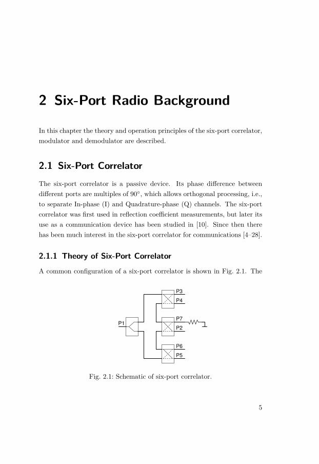
2.1 Six-Port Correlator
The six-port correlator is a passive device. Its phase difference betweendifferent ports are multiples of 90◦, which allows orthogonal processing, i.e.,to separate In-phase (I) and Quadrature-phase (Q) channels. The six-portcorrelator was first used in reflection coefficient measurements, but later itsuse as a communication device has been studied in [10]. Since then therehas been much interest in the six-port correlator for communications [4–28].
2.1.1 Theory of Six-Port Correlator
A common configuration of a six-port correlator is shown in Fig. 2.1. The
P1P7
P5
P6
P3
P4
P2
Fig. 2.1: Schematic of six-port correlator.
5
Chapter 2 Six-Port Radio Background
properties of this six-port correlator can directly be derived from its buildingblocks, i.e., the Wilkinson power divider and the three 90◦ hybrid couplers.Owing to the properties of the building blocks, an integer multiple of phasedifferences of 90◦ is presented between its ports. The same six-port cor-relator allows separation of I and Q channels in a six-port demodulator(receiver) and generation of a modulated radio frequency (RF) containing Iand Q data in a six-port modulator (transmitter). In both the demodulatorand modulator, only a single local oscillator (LO) source is required. Thecomplete S-parameter matrix for the six-port correlator can be found byinspection of Fig. 2.1:
with the relation between the incident waves a and reflected waves b (wherea and b are vectors) with respect to the six-port correlator, as follows:
b = Sa (2.2)
The ideal six-port correlator behavior was modeled by (2.1) and (2.2), andwill be used to derive and analyze the functionality of both the six-portmodulator and six-port demodulator.
2.2 Six-Port Modulator
For modulation, the six-port correlator can be used together with variableimpedance loads to generate the modulated RF signal [5, 16, 17, 29], seeFig. 2.2. The variable impedance loads are controlled by a baseband signaland are used to generate different reflection coefficients on the respective
6
2.2 Six-Port Modulator
Six-port correlator
P1P2
P3
P6
P7RF
LO
Z6
Z5Γ5
Z4Γ4
Z3
Γ6
Γ3
P5
P4
Fig. 2.2: Schematic of six-port modulator/transmitter.
ports on the six-port correlator. The variable reflection coefficients mod-ulate an applied carrier signal. The variable impedance loads are usuallyimplemented either by using switches [5, 17], transistors [15, 23, 29, 30] ordiodes [20,27].Carrier leakage is a problem that is likely present when using variable
impedance loads together with a six-port correlator for modulation [16,23],and leakage degrades the performance of the transmitter-receiver chain [16,31, 32]. To limit the effect of carrier leakage, balanced modulators can beused [29,30,33].
2.2.1 Building Blocks of Six-Port Modulator
The six-port modulator can be divided into two independent building blocks:the six-port correlator and the reflection coefficient generator. Combiningthese two blocks, the theory of the six-port modulator can be explained.
2.2.1.1 Six-Port Correlator
In a six-port modulator, as shown in Fig. 2.2, an LO source is connected toport P2 and generates an incident wave (a2), this wave experiences differentphase shifts and attenuations when it passes the six-port correlator to each
7
Chapter 2 Six-Port Radio Background
of the four output ports (P3 - P6). The transmitted or outgoing wavesbx on ports (P3 - P6) travel towards the impedance load Zx where it getsreflected. The reflected waves are now at the input on ports (P3 - P6) and apart of it is transferred to the output port P1. Owing to the phase relationsin the six-port correlator, and depending on how the impedance loads areselected, a modulated signal including both I and Q data can be generated.In an ideal six-port correlator, it is shown in Section 2.2.2 that the (complex)modulated output wave b1 at port P1 is
b1 = −a2
4 [(Γ3 + Γ4) + j (Γ5 + Γ6)] (2.3)
where a2 is the forward wave at port P2. Γ3, Γ4, Γ5 and Γ6 are the reflectioncoefficients at ports P3, P4, P5 and P6, as shown in Fig. 2.2. For modulationto occur, the value on Γ3 - Γ6 must change as a function of time.
2.2.1.2 Reflection Coefficient Generator
For generation of different reflection coefficients Γx, where x ∈ {3, 4, 5, 6} isthe port number, it is required to change the load impedance Zx at ports(P3 - P6) as a function of a control voltage or baseband signal Vx. Thereflection coefficient Γx is given by (2.4)
Γx (Vx) = Zx (Vx)− Z0,x
Zx (Vx) + Z0,x(2.4)
where Z0,x is the characteristic impedance on the transmission line (TL)connecting impedance load Zx to port Px on the six-port correlator. Observethat (2.4) is a nonlinear function of the impedance load.
2.2.2 Theory of Six-Port Modulator
To model the relation between the ports of the six-port correlator, S-parametersare used. The port numbers are defined as shown in Fig. 2.2. The outputport for the modulated signal is defined to be P1, whereas P2 is defined
8
2.2 Six-Port Modulator
to be the input port for the carrier (LO). Ports P3 and P4 constitute oneoutput port pair (P3, P4) and ports P5 and P6 the second output port pair(P5, P6). Define a reflection coefficient (Γ), incoming (a) and transmittedwave (b) on each of the ports P3, P4, P5 and P6
bx = Sx2a2 (2.5)
ax = Γxbx (2.6)
b1 = S1xax (2.7)
The three main steps to get a modulated output signal are: a) the incom-ing wave is transferred from the input port (P2) to all the other ports inthe six-port correlator resulting in the terms bx = Sx2a2, b) the transmittedwave bx is reflected on the load impedance Zx and gives an input wave atport Px, ax = Γxbx, and c) the input wave is transferred to the output port(P1), i.e., b1 = S1xax = S1xΓxSx2a2. The total output wave is the sum ofthe reflections from each of the loads at port P3 - P6:
Using the ideal S-parameters as given in (2.1), it results in
b1 = −a2
4 [(Γ3 + Γ4) + j (Γ5 + Γ6)] (2.9)
the value on the reflection coefficient Γx is in general complex. For mod-ulation to occur, the value on Γx must change as a function of time. It iscommon that Γ3 = Γ4 and Γ5 = Γ6. If the reflection coefficient is approxi-mated as a linear function of the applied baseband voltage V = VCM + ∆v
where ΓCM = Γ (VCM ) is generated by the constant common mode voltageVCM , and δ is the first derivative of Γ at VCM , i.e.,
δ = dΓdV|∆v=0 (2.11)
and ∆v the voltage deviation in the baseband signal that changes with time.Commonly the same type of impedance load is implemented on port pairs(P3, P4) and (P5, P6). If Γ3 = Γ4 = ΓI and Γ5 = Γ6 = ΓQ is used togetherwith (2.9) and (2.10) then
b1 = −a2
2 (ΓI + jΓQ) = −a2
2
ΓCM (1 + j)︸ ︷︷ ︸Carrier leakage
+ δ (∆vI + j∆vQ)︸ ︷︷ ︸RF Modulated
(2.12)
it is evident from (2.12) that only a part of the carrier signal a2 is modulatedto give the RF signal, whereas the other part gives an unwanted carrierleakage [20]. To avoid this leakage ΓCM = 0 is required.
2.2.3 Six-Port Modulator Architectures
Two different configurations exist for the implementation of the six-portcorrelator for use in six-port modulators: a series or a parallel configu-ration [16]. The parallel configuration generally gives better modulationperformance and hence most of the reported six-port modulators are basedon the parallel configuration [5, 16, 17, 29]. The main difference between re-ported modulators is therefore found in terms of how the impedance loadsare implemented and the modulation order they support. The three maintypes of impedance loads are:
• Switch matrices - vary the impedance in discrete steps.
• Transistors - vary the impedance in a continuous way by an analogcontrol signal.
• Diodes - vary the impedance in a continuous way by an analog controlsignal.
10
2.3 Six-Port Demodulator
Impedance loads implemented with switches posses a good linearity but,due to their limited speed, they are limited to low or moderate data rateapplications [5,17]. Impedance loads implemented with transistors or diodes[15,23,27,29,30] allow high speed operation, but may have limited linearity.
A common problem with six-port based modulators is carrier leakage. Thecarrier leakage gives rise to, for example, unwanted in-band emission of theLO and degrades the performance in the receiver that in turn may decreasethe channel capacity [34–36]. To decrease the impact of any present carrierleakage and to improve the modulation performance, balanced vector mod-ulators have been proposed [29,30,33]. Unfortunately, their implementationrequires several couplers and impedance loads, which results in increasedsystem complexity.
2.3 Six-Port Demodulator
For demodulation, the six-port correlator can be used together with powerdetection, i.e., utilizing second-order nonlinearity, to recover the basebandsignal [10,12,19,21,24], see Fig. 2.3. Schottky diodes are commonly used forpower detection and allow high date rate due to their high-speed property.To recover the baseband signal the modulated RF and a coherent LO areapplied to the six-port correlator. In other words, we are using the six-port demodulator in a direct conversion receiver. The phase relations in thesix-port correlator together with the nonlinear processing allow to separatethe I and Q baseband channels. The separated I and Q channels will, dueto the nonlinear processing, not only contain the wanted baseband I andQ signals, but also a dc offset. It is well known that dc offset is a seriousproblem in a direct conversion receiver because the dc offset overlaps thewanted baseband signal [31,34]. However, by taking the difference betweenport pairs (P3, P4) and (P5, P6) the dc offset can be effectively suppressedin the detected baseband I and Q channels.
11
Chapter 2 Six-Port Radio Background
Six-port correlator
−
+
−
+
P1P7
P5
P6
P3
P4
P2
I
Q
RF
LO
Power detectorBaseband recovery
Baseband recoveryPower detector
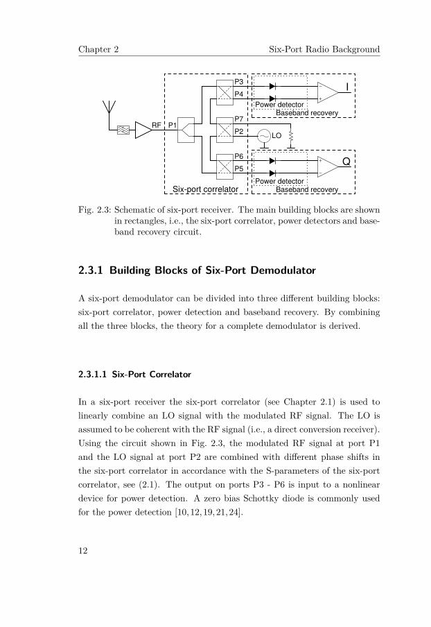
Fig. 2.3: Schematic of six-port receiver. The main building blocks are shownin rectangles, i.e., the six-port correlator, power detectors and base-band recovery circuit.
2.3.1 Building Blocks of Six-Port Demodulator
A six-port demodulator can be divided into three different building blocks:six-port correlator, power detection and baseband recovery. By combiningall the three blocks, the theory for a complete demodulator is derived.
2.3.1.1 Six-Port Correlator
In a six-port receiver the six-port correlator (see Chapter 2.1) is used tolinearly combine an LO signal with the modulated RF signal. The LO isassumed to be coherent with the RF signal (i.e., a direct conversion receiver).Using the circuit shown in Fig. 2.3, the modulated RF signal at port P1and the LO signal at port P2 are combined with different phase shifts inthe six-port correlator in accordance with the S-parameters of the six-portcorrelator, see (2.1). The output on ports P3 - P6 is input to a nonlineardevice for power detection. A zero bias Schottky diode is commonly usedfor the power detection [10,12,19,21,24].
12
2.3 Six-Port Demodulator
2.3.1.2 Power Detection
As previously mentioned a Schottky diode is usually used for the power de-tection, but any device with a (even-order) nonlinear characteristic can beused. The nonlinear transfer function of the diode will, among other fre-quencies, generate the demodulated baseband signal. A square law transferfunction is used to model the current IPD in an ideal power detector (PD)as a function of the applied voltage v.
IPD (v) = kv2 (2.13)
where k is a constant.
2.3.1.3 Baseband Recovery
The outputs from the diode pairs at port (P3, P4) and port (P5, P6) arethen fed to a differential baseband amplifier, as shown in Fig. 2.3. Takingthe difference between the diode output current on specified ports results inI and Q data in two different paths, without any dc offset in the ideal case.
2.3.2 Theory of Six-Port Demodulator
The complete demodulation process with a six-port correlator is now derived[21,37]. The modulated RF (z) and the LO (g) signals are described in thecomplex domain as follows:
z = ARF (XI + jXQ) ejωt (2.14)
g = ALOejφejωt (2.15)
where ω is the angular frequency, φ is the relative phase between RF andLO, ALO and ARF are the LO and RF amplitudes, respectively. XI and XQ
are the transmitted baseband I and Q data. The combined complex outputon port Px on the six-port correlator due to the RF input on port P1 and
13
Chapter 2 Six-Port Radio Background
the LO input at port P2 is
yx = Sx2g + Sx1z (2.16)
where x corresponds to one of the four output ports P3 - P6, i.e., x ∈{3, 4, 5, 6}, and Snm is the S-parameter forward transmission from port mto port n of the six-port correlator. The incident wave on port P1 is thereforea1 = z and on port P2 it is a2 = g. For modeling, an ideal power detectorwith a square law transfer function according to (2.13) is assumed. The realpart of yx:
Yx = <{yx} = yx + yx2 (2.17)
is used to calculate the time-domain signal. After power detection (squaring)and low-pass filtering (LPF) of the signal in (2.17), the time-domain outputvoltage Vx is given by:
Vx = LPF{kY 2
x
}= k
yxyx2 = k
|yx|2
2 (2.18)
Using (2.14) - (2.18) together with Euler’s formula and setting k = 1 forsimplicity results in, after some simplification, the following useful expres-sion:
Vx = |Sx2|2A2LO/2 + |Sx1|2A2
RF
(X2I +X2
Q
)/2 + (2.19)
ALOARF |Sx|XI cos (φ+ ∠Si) +
ALOARF |Sx|XQ sin (φ+ ∠Si)
where|Sx| = |Sx1||Sx2| (2.20)
∠Sx = ∠Sx2 − ∠Sx1 (2.21)
From (2.19) it is clear that the relative phase φ between the RF and LOsignals as well as the phase and gain relations in the six-port correlator affecthow much of XI and XQ that is present in the output signal Vx. Introducing
14
2.3 Six-Port Demodulator
Mx, Lx, Nx and R to keep the notations shorter:
Mx = |Sx2|2A2LO/2 (2.22)
Lx = |Sx1|2A2RF /2 (2.23)
Nx = ALOARF |Sx| (2.24)
R = X2I +X2
Q (2.25)
then (2.19) may be expressed in matrix formM3 L3 N3 cos∠S3 N3 sin∠S3
M4 L4 N4 cos∠S4 N4 sin∠S4
M5 L5 N5 cos∠S5 N5 sin∠S5
M6 L6 N6 cos∠S6 N6 sin∠S6
︸ ︷︷ ︸
D
1R
XI
XQ
=
V3
V4
V5
V6
(2.26)
This matrix model is used to describe the six-port demodulator. The matrixD is dependent on the actual implementation of the six-port correlator anddirectly related to the S-parameters of the six-port correlator. The LO poweris assumed to be known in the demodulator and therefore only XI , XQ andR are unknown. The S-parameters for the ideal six-port correlator are givenby:
from which the D matrix can be derived from (2.22) - (2.26)
D = 18
A2LO A2
RF −2ALOARF 0A2LO A2
RF 2ALOARF 0A2LO A2
RF 0 −2ALOARFA2LO A2
RF 0 2ALOARF
(2.28)
There are only three unknown variables in this linear model: XI , XQ andR, but four equations are available, therefore one of the equations is linearlydependent on the others and D is singular. By inspection of (2.28) togetherwith (2.26), it is seen that the detected I signal Id (I channel) can be recov-ered by taking the difference of V4 − V3, and the detected Q signal Qd (Qchannel) by taking the difference of V6 − V5:
Id = 2ALOARF
(V4 − V3) (2.29)
Qd = 2ALOARF
(V6 − V5) (2.30)
Both the dc offset from LO (Mx) and the nonlinear distortion (R) are can-celed on the I and Q channel outputs in this case. In an ideal system thedetected I-Q symbols should be an exact scaled copy of the transmittedsymbols, i.e., Id = kXI and Qd = kXQ where k is a scaling factor. Ina realistic system there may be phase and/or amplitude imbalances in thesix-port correlator and, therefore, crosstalk between I and Q channels.
2.3.3 Six-Port Demodulator Architectures
According to the derived theory of the six-port demodulator, to recover thebaseband I and Q channels with dc offset suppression, equation (2.29) -(2.30) must be implemented.
16
2.4 Six-Port Radio vs Conventional Radio
2.3.3.1 Direct Sampling of the Power Detector Output
One approach is to first amplify and low-pass filter each of the four outputsfrom the power detectors [4, 14, 26] and then sample the output with ananalog to digital converter (ADC) and implement (2.29) - (2.30) in thedigital domain. In this configuration four baseband amplifiers, four filtersand four ADCs are used. A challenge, if a ADC is used, to directly sampleeach of the four outputs of the power detectors is that they need to operate athigh-speed to support high symbol rates. The high-speed operation requiredfor the four ADCs increases the system cost and power consumption.
2.3.3.2 Using Differential Amplifier
Another approach is to use differential amplifiers [11,21,24,38] that are usedto implement (2.29) - (2.30), i.e., to take the difference between port pairsto recover the baseband I and Q channels. In this case, the number of ADCscan be reduced from four to two. An analog decision circuit may also beimplemented to directly demodulate the data without using any ADC ordigital signal processing [15,24,39]. Depending on the modulation used, ananalog decision circuit may be a good choice for high date rate applications.
2.4 Six-Port Radio vs Conventional Radio
In general, two main radio architectures exist, the heterodyne architectureand the direct conversion, or homodyne, architecture [31, 40]. Both havetheir respective pros and cons. The direct conversion architecture has gainedincreasing interest due to its simpler architecture. The six-port radio utilizesa direct conversion architecture. The equivalence between a conventionaldirect conversion radio using mixers and the six-port technique is clear fromthe previous theoretical discussion on six-port modulator and demodulatorand has been proved in [18]. The key differences between six-port radio andconventional radio based on mixers are therefore presented in the context ofa direct conversion architecture.
17
Chapter 2 Six-Port Radio Background
2.4.1 Reflection Based vs Mixer Based Modulator
As explained in Chapter 2.2, a six-port modulator generates the modulatedRF signal directly from an LO source (carrier) in terms of the reflection coef-ficients at specific ports. The reflection coefficients are generated from vari-able impedance loads. Hence, if the impedance is controlled by a basebandsignal, modulation is possible. This reflection based technique to generatea modulated signal is well known [30,33,41–43].In a reflection based modulator (six-port), the baseband I and Q data
control the reflection coefficient present at specific ports and the carrierwave is multiplied with these reflection coefficients to generate a modulatedRF signal. In a mixer based modulator, the baseband I and Q channels aremultiplied with the carrier by means of a mixer.Because the six-port is a passive and linear device, the output power
can be increased by increasing the LO power and the use of a PA can tosome extent be avoided. A typical mixer, based on diodes or transistors, iscertainly nonlinear and has therefore limited power handling capability. Thereflection based modulation technique, that is used in a six-port modulator,can be used with spectral shaping, linearization and digital predistortiontechniques. A modulated output signal with good properties in time andfrequency domain can thus be generated [42].
2.4.2 Power Detection Based vs Mixer Based Demodulator
In a six-port demodulator recovery of I and Q baseband signals are done byusing power detection at the four outputs of the six-port correlator. Owingto the relative phase differences between the four output ports, the twoinput waves, i.e., the RF and LO signals add constructively or destructivelyand this is detected by the power detector, commonly implemented witha Schottky diode [14, 18]. In a conventional mixer based direct conversiondemodulator, two mixer cores, one for I channel and one for Q channel, areused. The mixers commonly operate in switching mode, so its conductancechanges from a high to low state and thereby allows frequency conversion,
18
2.5 Challenges Associated with Six-Port Radio
i.e., demodulation. In general switching mode mixers require more LO powerthan power detection.
2.4.3 Pros and Cons of the Six-Port Radio
The previous section has discussed key differences between six-port mod-ulator/demodulator compared to a traditional direct conversion modula-tor/demodulator based on mixers. Performance evaluation on six-port ra-dio as well as comparative studies between six-port radio and conventionalmixer based radio can be found in the literatures [9,11,12,24,28,44]. Basedon these results, pros and cons of the six-port radio technique in comparisonwith a traditional direct conversion radio can be listed.
Pros:
• High bandwidth –> high data rate
• Passive circuit –> high linearity and low loss
• Power detection –> low power
• Six-port correlator is a distributed circuit –> scalable with frequency
Cons:
• Diode detectors –> low sensitivity
• Diode detectors –> limited dynamic range
• Six-port correlator is a distributed circuit –> large size at low fre-quency
2.5 Challenges Associated with Six-Port Radio
A six-port based modulator and demodulator, i.e., a six-port radio, sharemuch of the properties and challenges that are known from direct conversion
19
Chapter 2 Six-Port Radio Background
modulators and demodulators. Hence, much of the challenges associatedwith six-port radio is similar to the challenges for direct conversion radios[34,45,46].
2.5.1 Dc Offset
The dc offset is a serious problem in a direct conversion receiver (DCR) andhence in the six-port demodulator. Because the wanted baseband signalas well as the unwanted dc offset both are centered at dc, they can not beseparated by filtering. If the dc offset is severe, it may saturate the followingbaseband amplifiers.The dc offset can be divided into two types: a) a static dc offset, and b)
a dynamic dc offset. The static dc offset is assumed to be constant, or tochange slowly and can relatively easily be compensated for. The dynamic dcoffset is more problematic as it changes with time. Both types of dc offsetwill interfere with the baseband signal and degrade the receiver performanceor, if the dc offset is severe, even saturate stages in the receiver chain. Thereare several mechanisms that can generate dc offset, such as LO leakage andLO self-mixing [34,45,46].
2.5.2 LO Leakage
Due to finite isolation from LO to RF port, a part of the LO signal reachesthe RF port. This signal, i.e., the LO leakage or carrier leakage, gives riseto a number of problems:
• In a receiver, the LO leakage passes through the front end filter andamplifiers and reaches the antenna, where it is radiated. The radiatedLO leakage may be reflected in the environment and received by theantenna and upon mixing with the LO, contributing to the LO self-mixing.
• In a receiver (demodulator), the LO leakage reaches the RF input ofthe LNA and if the signal level is too high, it saturates the LNA and/or
20
2.5 Challenges Associated with Six-Port Radio
other blocks in the RF chain.
• In a modulator (transmitter) the LO leakage results in in-band LOradiation and decreased SNR.
These effects are clearly unwanted as it, among other things, contaminatesthe RF spectrum and degrades the performance of the receiver.
2.5.3 LO Self-Mixing
LO self-mixing is the case when a part of the LO signal reaches the RFinput port and mixes with itself. Several paths exist, due to finite isolationbetween the RF and LO ports. A part of the LO reaches the RF portand upon reaching the band-pass filter (BPF), LNA and antenna a part ofthe LO leakage is reflected back towards the RF input port of the six-portdemodulator and generates and unwanted dc signal at the output of thepower detectors that may interfere with the baseband data.
21
3 Six-Port Modulators in ThisStudy
For modulation, the six-port correlator can be used together with variableimpedance loads (see Fig. 3.1) to generate the modulated RF signal, asdiscussed in Chapter 2.2. The use of variable impedance loads is known tocreate problem with carrier leakage [16, 23]. A new approach to suppressthe carrier leakage is therefore presented and discussed in this study. Theproposed solution to suppress the carrier leakage is further investigated interms of its performance vs frequency and how it affects the modulationperformance, in terms of the error vector magnitude (EVM). As the finalstep a Schottky diode as a high-speed variable impedance load is proposedand analyzed. The Schottky diode based impedance load, together with thecarrier leakage suppression technique, allows for data rates above 1 Gbit/swith good modulation performance and suppressed carrier leakage.
3.1 Carrier Leakage Suppression
Carrier leakage is a problem that may be present when using variable loadstogether with a six-port correlator for modulation [16,23]. The carrier leak-age degrades the performance of the transmitter-receiver chain [16, 31, 32].One approach to limit the effect of carrier leakage is to use balanced mod-ulators [29,30,33]. However, balanced modulators require a complex circuitimplementation. Here a simple yet efficient method to suppress the carrierleakage is presented.
23
Chapter 3 Six-Port Modulators in This Study
Six-port correlator
P1P2
P3
P6
P7RF
LO
Z6
Z5Γ5
Z4Γ4
Z3
Γ6
Γ3
P5
P4
Fig. 3.1: Schematic of six-port modulator/transmitter.
3.1.1 Theory
It was shown in (2.12) in Section 2.2.2 that the presence of a static compo-nent of Γ, i.e., ΓCM 6= 0 generates an unwanted carrier signal at the outputport P1 of the six-port modulator. In general the following holds
b1 = −a2
4 [(Γ3 + Γ4) + j (Γ5 + Γ6)] (3.1)
where Γx is the reflection coefficient looking out at port Px of the six-portcorrelator. The value of Γx is dependent on three parameters: a) the loadinput impedance Zload,x (Vx), b) the characteristic impedance Z0,x of thetransmission line (TL) and c) the length lx of the TL connecting the outputat port Px to the load.
Γload,x (Vx) = Zload,x (Vx)− Z0,x
Zload,x (Vx) + Z0,x(3.2)
Γx = Γload,xe−j2βlx = Γload,xe−jθx (3.3)
where θx = 2βlx, β = 2π/λ, λ = vp/f and vp the phase velocity. Vx is acontrol voltage or baseband signal to change the impedance Zload,x to allowmodulation. The same impedance load device (such as a diode or transistor)
24
3.1 Carrier Leakage Suppression
is assumed to be used at ports P3 - P6 and, therefore, Γload,x = Γ whereΓ is the reflection coefficient at the load to TL interface and modeled by(2.10). Hence,
(3.4)where ∆Γx = δ∆vx as previously discussed in Section 2.2.2.
3.1.1.1 Carrier Leakage Suppression Without Modulation
When there is no modulation, i.e., ∆vx = 0 and ∆Γx = 0, the requirementon the output signal to have no carrier leakage is that b1 = 0. Using ∆Γx =0, (3.1) and (3.4) result in
b1 = −a2
4 |ΓCM |ej∠ΓCM
[(e−jθ3 + e−jθ4
)+ j
(e−jθ5 + e−jθ6
)](3.5)
It is possible to select the values of θx in (3.5) to force both the real andimaginary parts to zero, and therefore fulfill b1 = 0. The following twoconditions must then be fulfilled:
e−jθ3 = −e−jθ4 = e±jπe−jθ4 (3.6)
e−jθ5 = −e−jθ6 = e±jπe−jθ6 (3.7)
henceθm = θn ± π (3.8)
lm = ln ±λ
4 (3.9)
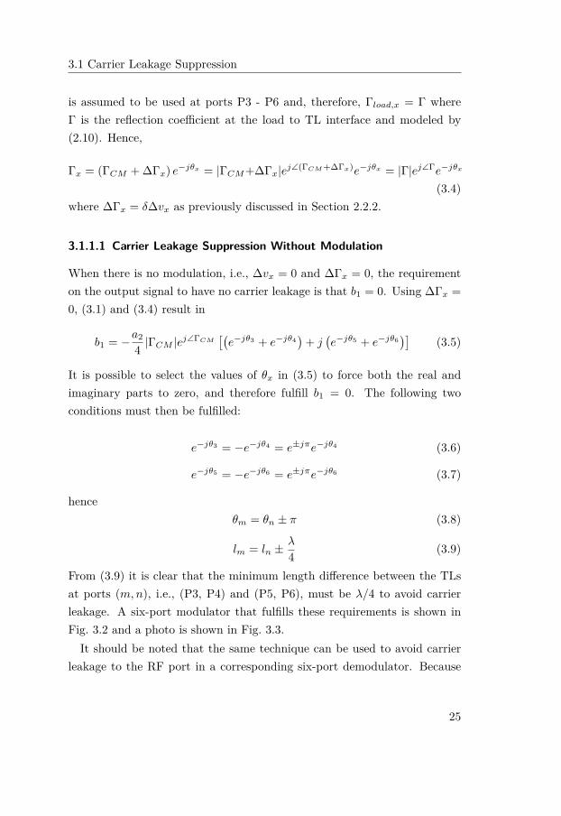
From (3.9) it is clear that the minimum length difference between the TLsat ports (m,n), i.e., (P3, P4) and (P5, P6), must be λ/4 to avoid carrierleakage. A six-port modulator that fulfills these requirements is shown inFig. 3.2 and a photo is shown in Fig. 3.3.It should be noted that the same technique can be used to avoid carrier
leakage to the RF port in a corresponding six-port demodulator. Because
25
Chapter 3 Six-Port Modulators in This Study
Six-port correlator
P1P2
P3
P6
P7RF
LO
Z6
Z5Γ5
Z4Γ4
′Γ4
Z3
Γ3
′
Γ6
Γ3
Γ6
′
Γ5
′
P5
P4
λ/4
λ/4
Fig. 3.2: Schematic of six-port transmitter with a carrier leakage suppressiontechnique [20].
any mismatch at the detector diodes in a six-port demodulator will gener-ate a static ΓCM 6= 0 and thus exactly the same analysis and solution, asdiscussed here holds for demodulators. Carrier leakage in six-port demodu-lators is further discussed in Section 4.4.
3.1.1.2 Carrier Leakage Suppression for Modulation
If the requirement for no carrier leakage is satisfied as derived in Sec-tion 3.1.1.1, for example by selecting θ3 = θ5 = 0 and θ4 = θ6 = π, itfollows from (3.4)
Γ3 = (ΓCM + ∆Γ3) (3.10)
Γ4 = − (ΓCM + ∆Γ4) (3.11)
ΓI = Γ3 + Γ4 = ∆Γ3 −∆Γ4 = δ (∆v3 −∆v4) (3.12)
The common and unwanted part ΓCM cancels out and only the modulatingpart ∆Γx remains. The same principle holds for the Q channel, i.e., ΓQ. Toavoid offsetting the IQ constellation, and also to avoid a carrier leakage, the
26
3.1 Carrier Leakage Suppression
Fig. 3.3: Photo of implemented six-port modulator with a technique for car-rier leakage suppression [20].
expected (mean) value of I and Q channel must be zero, i.e.,
E {ΓI} = E {ΓQ} = 0 (3.13)
If the voltages on the I-channel are selected according to
∆v3 = kXI (3.14)
∆v4 = −kXI = −∆v3 (3.15)
where XI is the modulating symbol for I-channel and k a scaling factor.
27
Chapter 3 Six-Port Modulators in This Study
Using (3.14) - (3.15) in (3.12)
ΓI = 2δkXI (3.16)
a similar result holds for the Q-channel
ΓQ = 2δkXQ (3.17)
and it is assumed that E {XI} = E {XQ} = 0 so there is no carrier leakage.If there is a gain difference ε and an offset voffset on ∆v4 compared to
∆v3, i.e.,∆v4 = −kXI (1 + ε) + voffset (3.18)
it follows from (3.12) that
ΓI = δkXI (1 + 1 + ε)︸ ︷︷ ︸E{·}=0
+ δvoffset︸ ︷︷ ︸E{·}6=0
(3.19)
which shows that a gain difference will not generate any carrier leakage. Onthe other hand, any offset voffset 6= 0 will then contribute to the carrierleakage. Another observation is that if ε = −1 the value of ∆v4 = 0, sothere is no need to modulate the load connected at port P4, i.e., a singleended baseband control signal can be used. A single ended baseband controlsignal may simplify the circuit, but will also lower the output power by 6dB compared to the case when a differential baseband control signal is used(for ε = 0). In both cases the common mode voltage VCM (that generatesΓCM ) must be the same to suppress the carrier leakage.
3.1.2 Results
A six-port modulator was implemented to verify the carrier leakage sup-pression technique proposed in this study. The six-port modulator uses anadditional λ/4 transmission line at port P4 and P6 as shown in Fig. 3.2 andFig. 3.3. The output power spectrum was measured for a QPSK signal at 100
28
3.1 Carrier Leakage Suppression
Msymbol/s. As seen in Fig. 3.4 the carrier leakage is efficiently suppressed.Another benefit with the proposed carrier leakage suppression technique,when used with differential baseband control signals, is that it improves thelinearity. This is illustrated in Fig. 3.5 for a 16-QAM modulated signal.
7.1 7.2 7.3 7.4 7.5 7.6 7.7 7.8 7.9−80
−70
−60
−50
−40
−30
Frequency (GHz)
Sp
ectr
um
(d
Bm
/MH
z)
Fig. 3.4: Measured spectrum for a QPSK signal at 100 Msymbol/s. Owing tothe use of λ/4 TL at specific ports the carrier leakage is suppressed[20].
29
Chapter 3 Six-Port Modulators in This Study
−3 −1 1 3
−3
−1
1
3
(a) Differential control signal.−3 −1 1 3
−3
−1
1
3
(b) Non-differential control signal.
Fig. 3.5: Measured constellations for 16-QAM @ 100 Msymbol/s. Whendifferential and non-differential control voltages are used [20].
30
3.2 Impact of Phase Shifting Network on Carrier Leakage Suppression andEVM
3.2 Impact of Phase Shifting Network on CarrierLeakage Suppression and EVM
As shown in Section 3.1.1.1, one way to ensure low carrier leakage is to havea 90◦ phase shift between ports in each port pair (P3, P4) and (P5, P6),respectively. In general the phase shift and amplitude scaling between theports in a port pair will deviate from their ideal values when the actualfrequency deviates from the center (designed) frequency f0. Operating at afrequency where the amplitude and/or phase shift is not ideal will degradethe carrier leakage suppression and EVM performance. Hence a model topredict the performance as a function of the S-parameters of the phaseshifting network is derived. Using the derived model, a wideband phaseshifting network is proposed and optimized. A six-port modulator using thewideband phase shifting network is shown in Fig. 3.6.
3.2.1 Theory
The reflection coefficient Γx looking out of port Px of the six-port andtowards the phase shifting network (the two port network) is given by
Γx = S11 + S12S21ΓL,x1− S22ΓL,x
(3.20)
where ΓL,x is the reflection coefficient looking into the impedance load Zxand modeled according to (2.10), i.e.,
ΓL,x = ΓCM + ∆Γx (3.21)
The S-parameters for the phase shifting network are assumed to be givenby
S =[
0 Ae−jφ
Ae−jφ 0
](3.22)
31
Chapter 3 Six-Port Modulators in This Study
Six-port correlator
P1P2
P3
P6
P7RF
LO
Z6
Z5Γ5
Γ4
Γ6
Γ3
P5
P4
ΓL,6
ΓL,5
Z4
Z3
ΓL,4
ΓL,3
Fig. 3.6: Schematic of the six-port modulator using a broadband phase shift-ing network to suppress carrier leakage [47].
where S12 = S21 = Ae−jφ and A the amplitude scale factor and φ the phaseshift. Calculating for I-channel ΓI = Γ3 + Γ4 and by using ∆Γ3 = −∆Γ4 =∆Γ it follows from (3.20) - (3.22)
ΓI = Γ3 + Γ4 = ΓL,3 +A2e−j2φΓL,4= ΓCM
(1 +A2e−j2φ
)︸ ︷︷ ︸Carrier leakage
+ ∆Γ(1−A2e−j2φ
)︸ ︷︷ ︸Modulated RF
(3.23)
where φ = 0 and A = 1 were used for the phase shifting network responsiblefor Γ3. As expected from previous analysis, when A = 1 and φ = 90◦ thereis no carrier leakage and ΓI = 2∆Γ. If A 6= 1 and/or φ 6= 90◦ the ΓI vectoris distorted resulting in both carrier leakage and EVM degradation. Owingto circuit symmetry the same analysis holds for the Q-channel as well.
3.2.1.1 Carrier Leakage Dependence on Amplitude and PhaseMismatch
To find the carrier leakage (3.23) is used with ∆Γ = 0. For matched ports,the transmitted output power PTX = |b1|2/2 is related to the LO power
32
3.2 Impact of Phase Shifting Network on Carrier Leakage Suppression andEVM
PLO = |a2|2/2 by (3.1)
PTX = PLO16
(|ΓI |2 + |ΓQ|2
)(3.24)
The same impedance loads Zx are assumed to be used on ports P3 - P6,therefore ΓQ = ΓI . Using (3.23) in (3.24) it follows that the leakage powerratio Rleakage is
Rleakage = PTXPLO
|∆Γ=0 = |ΓCM |2
8 Ef (3.25)
whereEf = 1 +A4 + 2A2 cos (2φ) (3.26)
is the error function and is dependent on the actual amplitude A and phase φof the phase shifting network. In the ideal case A = 1, φ = 90◦ and Ef = 0,so there is no carrier leakage according to (3.25). Hence by knowing howA and φ vary with frequency, i.e., if the S-parameters of the phase shiftingnetwork are known, the carrier leakage suppression can be predicted.
3.2.1.2 EVM Dependence on Amplitude and Phase Mismatch
The EVM is given by [48]
EVM =
√1N
∑(|ΓI − ΓI,ref |2 + |ΓQ − ΓQ,ref |2)1N
∑(|ΓI,ref |2 + |ΓQ,ref |2)
(3.27)
Owing to symmetry both the I and Q channels will be affected in the sameway so only the I channel is calculated. The reference (ideal) ΓI,ref magni-tude square is found by using A = 1 and φ = 90◦ in (3.23)
using (3.28) and (3.29) in (3.27) the EVM is then found to be
EVM =√Ef
√∑(|ΓCM −∆ΓI |2 + |ΓCM −∆ΓQ|2)∑
(4|∆ΓI |2 + 4|∆ΓQ|2) (3.30)
The EVM is therefore proportional to the square root of the error functionEf . For the special case ΓCM = 0 there is no carrier leakage according to(3.25) and the EVM is only dependent on Ef as EVM|ΓCM =0 =
√Ef/2.
The link between EVM and Ef and therefore to the S-parameters of thephase shifting network can be utilized to design a phase shifting networkwith good performance.
3.2.2 Broadband Phase Shifting Network Using LoadedTransmission Lines
A phase shifting network based on adding a TL of length λ/4 at specificports, e.g., at port P4 and P6 as shown in Fig. 3.2, works well for narrow-band applications. However, for more wideband applications, a broadbandphase shifting network should be used. Between many possible solutions ourapproach is based on a loaded transmission line [49]. A six-port modulatorusing a phase shifting network based on the loaded transmission line isshown in Fig. 3.6. Referring to Fig. 3.7, the references branch is a TLwith an electrical length φr = 270◦. In the other branch a TL of electricallength 2φm = 180◦ is loaded with an open circuit (O.C) stub at the centerwith length φs = 180◦. All electrical lengths are defined at the centerfrequency f0. Compared to a single TL, the loaded TL helps to keep thephase difference close to 90◦ over a wider bandwidth. Amplitude and phasevariations over frequency depend on the impedances Zm and Zs. Hence thephase shifting network can be optimized for carrier leakage suppression and
34
3.2 Impact of Phase Shifting Network on Carrier Leakage Suppression andEVM
Zm, φm Zm, φm
Zr, φr
Zs, φs
O.C
Port P1 Port P2
Port P4Port P3
Fig. 3.7: Broadband phase shifter using a loaded transmission line [47].
the minimum EVM degradation, if the optimization goal is to minimize Efover the frequency range of interest.
3.2.3 Results
Since the use of λ/4 TL is a narrow-band phase shifting network, the per-formance will degrade outside of the center frequency. The simulated per-formance of Ef , and therefore the carrier leakage suppression according to(3.25), for a phase shifting network based on a TL and for the broadbandphase shifting network is compared in Fig. 3.8. In the simulation an ideal six-port correlator is used. Hence by implementing the broadband phase shiftingnetwork instead of the λ/4 TL the carrier leakage can be suppressed over amuch wider bandwidth. For an EVM of less than 10% requires Ef ≤ −14dB. An EVM of less than 10% is achived with the broadband phase shift-ing network over a relative bandwidth of about 60%, to compare with therelative bandwidth of about 12% for the λ/4 TL phase shifting network.
35
Chapter 3 Six-Port Modulators in This Study
0.6 0.7 0.8 0.9 1 1.1 1.2 1.3 1.4
−40
−35
−30
−25
−20
−15
−10
−5
0
Normalized frequency (f / f0)
Ef (
dB
)
OC
SC
TL
Fig. 3.8: Simulated Ef for a transmission line phase shifting network (TL)and for the optimized broadband phase shifting network terminatedwith an open circuit (OC) and short circuit (CS) [47].
36
3.3 Schottky Diode as High-Speed Variable Impedance Load
3.3 Schottky Diode as High-Speed VariableImpedance Load
The technique for carrier leakage suppression can be used with an arbitrarytype of impedance load. The optimal type of impedance load to use in aparticular situation depends on the actual requirements. Due to its fastspeed but low complexity, a Schottky diode is proposed to be used as thevariable impedance load instead of a switch or a transistor.
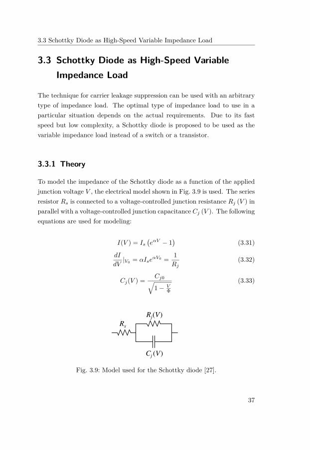
3.3.1 Theory
To model the impedance of the Schottky diode as a function of the appliedjunction voltage V , the electrical model shown in Fig. 3.9 is used. The seriesresistor Rs is connected to a voltage-controlled junction resistance Rj (V ) inparallel with a voltage-controlled junction capacitance Cj (V ). The followingequations are used for modeling:
I(V ) = Is(eαV − 1
)(3.31)
dI
dV|V0 = αIse
αV0 = 1Rj
(3.32)
Cj(V ) = Cj0√1− V
Φ
(3.33)
Cj (V)
Rj(V)
Rs
Fig. 3.9: Model used for the Schottky diode [27].
37
Chapter 3 Six-Port Modulators in This Study
where Is is the saturation current, α = n qkT , q is the electron charge, k
Boltzmann’s constant, T the temperature in Kelvin, Φ is the junction po-tential, and n the ideality factor. Combining (3.31) and (3.32) to expressRj as a function of the current I and Is:
Rj (V ) = 1α (I (V ) + Is)
(3.34)
The junction impedance Zj , i.e., the parallel combination of Rj and Cj canbe expressed as:
Zj = Req − jXeq (3.35)
where
Req = Rj1 + ω2R2
jC2j
(3.36)
Xeq =ωR2
jCj
1 + ω2R2jC
2j
(3.37)
The parasitic inductance from the package may be absorbed into Xeq, andthe series resistor Rs in the diode absorbed in Req.
The junction capacitance Cj (V ) and junction resistance Rj (V ) are biasdependent according to (3.33) and (3.34). Therefore, the junction impedanceZj can be controlled by changing the applied voltage V to the diode.
The reflection coefficient Γ, looking into the load from a TL of charac-teristic impedance Z0, is given by (3.38). When the diode parameters, LOpower and the bias voltage V are known, Γ can be calculated.
Γ = Zj − Z0
Zj + Z0=
R2eq +X2
eq − Z20
(Req + Z0)2 +X2eq
− j 2XeqZ0
(Req + Z0)2 +X2eq
(3.38)
38
3.3 Schottky Diode as High-Speed Variable Impedance Load
3.3.2 Results
Simulated and measured performance of the Schottky diode based impedanceload is presented in the following two sections.
3.3.2.1 Impact of LO Power on Reflection Coefficient
The impedance of the Schottky diode is dependent on the dc current presentin the diode, according to (3.31) - (3.37). The dc current is not only de-pendent on the applied bias voltage, but also on the applied LO power. Apart of the applied LO signal is rectified to a dc current and, therefore, con-tribute to the total dc bias current [50]. To observe the effect of LO powerof the reflection coefficient Γ, harmonic balance simulation in Advanced De-sign System (ADS) from Agilent Technologies Inc. is used. In Fig. 3.10 thereflection coefficient for LO power of -10, -5, 0 and 5 dBm are shown. Forlow LO power levels, the reflection coefficient is mainly controlled by theapplied dc voltage. For high LO power levels, the reflection coefficient Γis dependent on both the dc bias and the LO power used. The simulationverified the predicted dependence on LO power.
3.3.2.2 Measured Constellations
To verify that the Schottky diode is a suitable solution for high-speed ap-plications, measurements on the prototype modulator have been conducted.In the measurements a 16-QAM modulated signal at 100 and 300 Msym-bol/s was used. The corresponding data rates are thus 400 Mbit/s and 1.2Gbit/s, respectively. The results shown in Fig. 3.11 prove that Schottkydiodes can be used to implement variable impedance loads that supportsboth high order modulation and data rates above 1 Gbit/s in a six-portmodulator. Higher symbol rates than 300 Msymbols/s could not be verifieddue to limitations in the baseband generator that was used.
39
Chapter 3 Six-Port Modulators in This Study
0.2
0.5
1.0
2.0
5.0
+j0.2
−j0.2
+j0.5
−j0.5
+j1.0
−j1.0
+j2.0
−j2.0
+j5.0
−j5.0
0.0 ∞
PLO
= −10 dBm
PLO
= −5 dBm
PLO
= 0 dBm
PLO
= 5 dBm
Fig. 3.10: Simulated Γ vs applied voltage and for different values of PLO [27].
−3 −1 1 3
−3
−1
1
3
(a) 100 Msymbol/s = 400 Mbit/s.−3 −1 1 3
−3
−1
1
3
(b) 300 Msymbol/s = 1.2 Gbit/s.
Fig. 3.11: Measured constellations for 16-QAM signal [27].
40
3.4 Summary
3.4 SummaryThe problem with carrier leakage in a six-port modulator was investigatedand a solution presented. Our solution, based on a phase shifting networkdelivering a 90◦ phase difference between specific ports, is easy to implement.In its most simple form, a λ/4 TL may be used.The performance of the carrier leakage suppression and the modulation
performance in terms of EVM were further investigated as a function ofthe phase shifting network. Both carrier leakage suppression and the EVMperformance can be described by the same error function. The error functionis directly related to the amplitude and phase behavior of the phase shiftingnetwork, i.e., it is related to the S-parameters of the phase shifting network.For wideband performance, a loaded TL was proposed as one possible
solution to implement the phase shifting network. It was designed andoptimized with help of the derived error function.The use of Schottky diodes as high-speed variable impedance loads was
proposed and investigated. A six-port modulator using Schottky diodes asvariable impedance loads, including the carrier leakage suppression tech-nique was implemented. Measurements verified the carrier leakage suppres-sion technique and showed good modulation performance for a 16-QAMmodulated signal with a data rate of 1.2 Gbit/s. The data rate was limitedby the available measurement equipment.
41
4 Six-Port Demodulators in ThisStudy
It was shown in Chapter 2.3 how the six-port correlator can be used togetherwith power detection to recover the baseband signal. In this chapter, theperformance of a typical six-port demodulator, see Fig. 4.1, is presentedtogether with improvements of the architecture to support:
• High-speed processing
• Low power consumption
• Low circuit complexity
Six-port correlator
−
+
−
+
P1P7
P5
P6
P3
P4
P2
I
Q
RF
LO
Power detectorBaseband recovery
Baseband recoveryPower detector
Fig. 4.1: Schematic of a conventional six-port receiver.
43
Chapter 4 Six-Port Demodulators in This Study
4.1 Demodulator for High Data Rate
Six-port demodulators have previously mostly been shown with relativelylow date rates, well below 1 Gbit/s [22, 24]. To prove that the six-port isuseful for high-speed operation above 1 Gbit/s, a prototype was developed tooperate at the upper UWB frequency band with a designed center frequencyof 7.5 GHz. The performance of the prototype demodulator is characterizedin terms of BER and EVM for different data rates [21].
4.1.1 Theory
It is well known from Shannon’s theorem that the channel capacity C isrelated to the bandwidth B and SNR according to:
C = B log2
(1 + S
N
)(4.1)
The bit rate Rb is related to the symbol rate Rs and modulation order Maccording to [48]:
Rb = Rs log2M (4.2)
Using Rb = 1 Gbit/s and M = 16, i.e., 16-QAM results in Rs = 250Msymbol/s.According to Shannon’s theory and the required symbol rate Rs = 250
Msymbol/s, gigabit speed should be possible when operating in the upperUWB 6 - 8.5 GHz due to the wide bandwidth that is available. Hence,the limitations for gigabit speed are not in the six-port correlator itself.For power detection, Schottky diodes are used. Schottky diodes are fastand should not be the limiting factor for gigabit speed. The limitationsto achieve high-speed operation are therefore found in the baseband chain:baseband amplifiers and ADCs. These components have been identified asthe bottleneck in other studies as well [22,24]. To build a demodulator thatsupport high-speed, state of the art current mode high-speed operationalamplifiers were used to build the baseband amplifier to recover the I and
44
4.1 Demodulator for High Data Rate
Q baseband channels, see Fig. 4.2. The measured characteristics of theimplemented baseband amplifier, shown in Fig. 4.4, show that the requiredsymbol rate (250 Msymbol/s) to achieve at least 1 Gbit/s is supported.
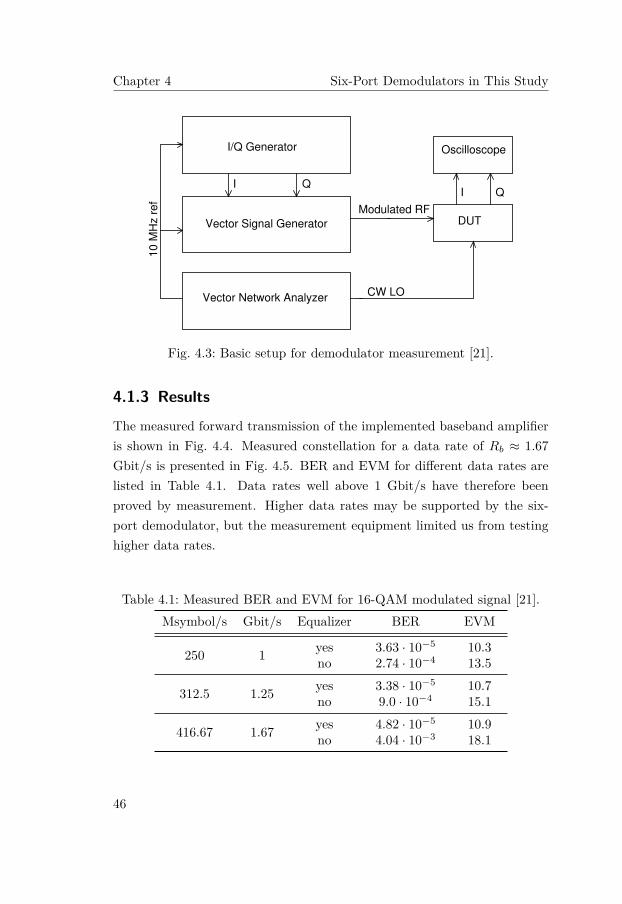
4.1.2 Measurement Setup
The measurement setup shown in Fig. 4.3 is the basic setup for all demodu-lator measurements. The I and Q data vectors are generated in a MATLABprogram, before they are transfered to the I/Q generator. The analog I andQ channels from the I/Q generator are connected to a vector signal gener-ator to modulate a carrier. The modulated output from the vector signalgenerator is then fed to the device under test (DUT), i.e., to the RF port ofthe six-port demodulator. An (ideally) coherent LO signal is connected tothe LO port of the six-port demodulator. The baseband I and Q channelsat the six-port demodulator are connected to an oscilloscope to sample thewaveform. The I and Q waveforms are sampled by a MATLAB program.The received waveform can then be processed and compared with the trans-mitted waveform to, for example, estimate the EVM and BER performance.
−
+
−
+
LMH6703
300
100
100
−
+
LMH6703
300
100
100
100
100
300
300
LMH6703
In1
In2
Out
Fig. 4.2: Differential amplifier for baseband recovery [21].
45
Chapter 4 Six-Port Demodulators in This Study
Vector Signal Generator
I/Q Generator Oscilloscope
DUT
Vector Network Analyzer
Modulated RF
CW LO
10
MH
z r
ef
I QI Q
Fig. 4.3: Basic setup for demodulator measurement [21].
4.1.3 Results
The measured forward transmission of the implemented baseband amplifieris shown in Fig. 4.4. Measured constellation for a data rate of Rb ≈ 1.67Gbit/s is presented in Fig. 4.5. BER and EVM for different data rates arelisted in Table 4.1. Data rates well above 1 Gbit/s have therefore beenproved by measurement. Higher data rates may be supported by the six-port demodulator, but the measurement equipment limited us from testinghigher data rates.
Table 4.1: Measured BER and EVM for 16-QAM modulated signal [21].Msymbol/s Gbit/s Equalizer BER EVM
250 1 yesno
3.63 · 10−5
2.74 · 10−410.313.5
312.5 1.25 yesno
3.38 · 10−5
9.0 · 10−410.715.1
416.67 1.67 yesno
4.82 · 10−5
4.04 · 10−310.918.1
46
4.1 Demodulator for High Data Rate
200 400 600 800 1000 1200 1400−10
0
10
20
30
Frequency (MHz)
Magnitude (
dB
)
Channel 1
Channel 2
Fig. 4.4: Measured forward transmission (S21) of the baseband amplifier[21].
(a) Without equalizer. (b) With equalizer.
Fig. 4.5: Measured constellation at 1.67 Gbit/s [21].
47
Chapter 4 Six-Port Demodulators in This Study
4.2 Diode Configurations in Six-PortDemodulator
It was shown in Chapter 2.3 that by taking the difference between the diodeoutput current on specific ports, the baseband I and Q channels can berecovered. For instance, to detect the I (Q) channel the difference betweenV4 (V6) and V3 (V5) must be calculated according to (2.29) - (2.30). As shownin Fig. 4.1 and Fig. 4.6a, this can be done by using a differential amplifier.However, some drawbacks and limitations can be identified compared tothat if an RF transistor is used:
• Speed limitations
• Power consumption
• Complexity and cost
The same drawbacks occur if ADCs are used to sample each of the fouroutput ports directly. Owing to these limitations and drawbacks, an alter-native way to recover the baseband I and Q channels that do not requireuse of differential amplifiers or ADCs are required to support high-speedoperation.The calculation of the difference can also be done by interchanging the
diode orientation on one of the diodes on each port pair (P3, P4) and (P5,P6), see Fig. 4.6b. In this way the baseband signal can still be recovered, butthere is no need to use a differential amplifier. Avoiding the use of two (I andQ channel) differential amplifiers simplifies the circuit and allows for higherprocessing speed. If the recovered baseband signal needs to be amplified, asingle ended amplifier can be used, such as a RF transistor for high-speedprocessing.
4.2.1 Theory
Three different approaches to calculate the difference of the signals betweenport pairs (P3, P4) and (P5, P6) are shown in Fig. 4.6. The configuration
48
4.2 Diode Configurations in Six-Port Demodulator
in Fig. 4.6a is commonly used and also useful to model the demodulator.The diode current id,x at port Px can be approximated by:
id,x (vd,x) = k1vd,x + k2v2d,x + k3v
3d,x + · · · (4.3)
where vd,x is the applied voltage over the diode junction connected to portPx on the six-port correlator. This voltage is a linear combination of theRF and LO signals applied to the six-port correlator. By using the results
−
+vx
vy
ix
iy
iout
(a)
ix
iy
vx
vy
iout
(b)
-180
-180
vx
vy
ia
ib
ic
id
ioy
iox
iout
(c)
Fig. 4.6: Diode configurations in six-port demodulator [19].
49
Chapter 4 Six-Port Demodulators in This Study
from Section 2.3.2, the voltages and currents related to I-channel is foundby using the S-parameters in (2.27) together with (2.14) - (2.17) to get vd,3and vd,4:
2vd,3 = ALO cos (ωt) +ARF [−XI cos (ωt) +XQ sin (ωt)] (4.4)
2vd,4 = −ALO sin (ωt) +ARF [−XI sin (ωt)−XQ cos (ωt)] (4.5)
where φ = 0 was assumed. The corresponding currents, assuming kn = 0for n ≥ 3, are found from (4.3) to:
id,3 (vd,3) = k1vd,3 + k2
A2LO
8 + A2RF
8(X2I +X2
Q
)︸ ︷︷ ︸
dc offset
−ALOARF4 XI
+ · · ·
(4.6)
id,4 (vd,4) = k1vd,4 + k2
A2LO
8 + A2RF
8(X2I +X2
Q
)︸ ︷︷ ︸
dc offset
+ALOARF4 XI
+ · · ·
(4.7)
the “· · · ” are terms due to second harmonic frequency components at 2f ,which are assumed to be suppressed together with the fundamental fre-quency components f by a low-pass filter. The bracket part {·} in (4.6) -(4.7) describes signals at dc, it includes the wanted baseband signal togetherwith unwanted dc offset.
4.2.2 Baseband Recovery with Differential Amplifier
If a differential amplifier, as shown in Fig. 4.6a, is used to take the difference:
iout = G (id,4 (vd,4)− id,3 (vd,3)) (4.8)
50
4.2 Diode Configurations in Six-Port Demodulator
the output signal after low-pass filtering, i.e., the baseband signal is:
iout,BB = Gk2ALOARF
2 XI (4.9)
where G is the gain of the differential amplifier. The three main reasons tocalculate the difference, found by inspecting (4.6) - (4.7), are to:
• Double the amplitude of the wanted baseband signal
• Suppress the static dc part from the LO source
• Suppress the dynamic dc offset from rectification of I and Q data
4.2.3 Baseband Recovery without Differential Amplifier
To avoid the use of a differential amplifier, the anode-cathode side of oneof the diodes (in this case the diode related to id,3) may be interchanged asshown in Fig. 4.6b and the output current is:
iout = id,4 (vd,4)− id,3 (−vd,3) (4.10)
However, k2 (vd)2 = k2 (−vd)2 so after low-pass filtering the baseband signalis:
iout,BB = k2ALOARF
2 XI (4.11)
therefore, the only difference between (4.9) and (4.11) is the gain factor G.This gain can easily be compensated for by using a single ended amplifierafter the low-pass filter, see Fig. 4.6b. To relax the requirement on thelow-pass filter, the diode configuration shown in Fig. 4.6b can be modifiedto the one shown in Fig. 4.6c. The additional benefit is that odd-orderharmonics are suppressed due to the relative phase difference of 180◦ at thefundamental frequency between the two parallel diode pairs.
51
Chapter 4 Six-Port Demodulators in This Study
4.2.4 Results
The demodulation performance was measured for a 16-QAM signal at 100Msymbol/s, i.e., a data rate of 400 Mbit/s. The RF and LO inputs are di-rectly applied to the six-port correlator and the recovered I and Q basebandsignals are measured and compared with the transmitted I and Q signals forEVM calculation. No impedance matching was used for the diodes. Hence,performance may likely be improved by using impedance matching at thecost of a more complex circuit.
4.2.4.1 Constellation
The measured constellations at the sensitivity limit, i.e., for a BER ≤ 10−3
is shown in Fig. 4.7 where the diode configuration shown in Fig. 4.6b andFig. 4.6c is used. Good performance and high-speed operation are thereforepossible without the use of differential amplifiers. The measured sensitivitylevels are -33 and -44 dBm at a LO power of 6 dBm for the diode configura-
−3 −1 1 3
−3
−1
1
3
(a) Diode configuration without har-monic suppression.
−3 −1 1 3
−3
−1
1
3
(b) Diode configuration with harmonicsuppression.
Fig. 4.7: Measured constellations for 16-QAMmodulation at 100 Msymbol/s[28].
52
4.2 Diode Configurations in Six-Port Demodulator
tion without (see Fig. 4.6b) and with (see Fig. 4.6c) harmonic suppression,respectively.
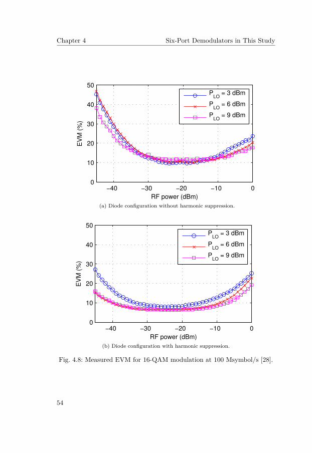
4.2.4.2 EVM
The EVM for different LO power levels PLO ∈ {3, 6, 9} dBm, and whenthe RF power is sweped from PRF = −45 dBm to PRF = 0 dBm is shownin Fig. 4.8. The EVM in Fig. 4.8b shows a more flat and lower EVM vsRF power compared to the EVM in Fig. 4.8a. In this case, better EVMperformance over a larger RF power range can be achieved when the diodeconfiguration with odd-order harmonic suppression is used.
53
Chapter 4 Six-Port Demodulators in This Study
−40 −30 −20 −10 00
10
20
30
40
50
RF power (dBm)
EV
M (
%)
P
LO = 3 dBm
PLO
= 6 dBm
PLO
= 9 dBm
(a) Diode configuration without harmonic suppression.
−40 −30 −20 −10 00
10
20
30
40
50
RF power (dBm)
EV
M (
%)
P
LO = 3 dBm
PLO
= 6 dBm
PLO
= 9 dBm
(b) Diode configuration with harmonic suppression.
Fig. 4.8: Measured EVM for 16-QAM modulation at 100 Msymbol/s [28].
54
4.3 Baseband Complexity Comparison of Six-, Five-, and Four-PortDemodulators
4.3 Baseband Complexity Comparison of Six-,Five-, and Four-Port Demodulators
With the new diode configurations that allows high-speed processing, thecircuit complexity was reduced which also implies that the power consump-tion can be decreased. Other multi-port structures, like the five-port andfour-port, have also been proposed to simplify the complexity in recoveringthe baseband signal. In a five-port receiver only three ports are used forbaseband recovery and in a four-port receiver two ports are used to recoverthe baseband data. It can be shown mathematically that three output portsare required to demodulate, i.e., to recover the baseband data. Hence, a six-port has one “extra” port that is not strictly required, but simplifies thebaseband receovery circuit. The four-port receiver only works with someadditional constraints on the RF and LO signals.
4.3.1 Analysis of Baseband Complexity
In a six-port receiver shown in Fig. 4.1 there are four outputs (P3 - P6)and hence four equations are available. There is one more equation thanunknown variables. Therefore, one equation can be removed, i.e., one of theoutput port can be removed. This results in a five-port [37, 51, 52]. Thethree remaining outputs allow to calculate XI , XQ and R = X2
I +X2Q. One
possible configuration of a five-port receiver is shown in Fig. 4.9 [51]. Usingthe same approach as in Section 2.3.2, the corresponding equation in matrixform is then
L3 N3 cos∠S3 N3 sin∠S3
L4 N4 cos∠S4 N4 sin∠S4
L5 N5 cos∠S5 N5 sin∠S5
R
XI
XQ
=
V ′3
V ′4
V ′5
(4.12)
where V ′x = Vx − Mx. The D matrix is found by inspection of the S-parameters for the five-port configuration shown in Fig. 4.9:
55
Chapter 4 Six-Port Demodulators in This Study
Five-port correlator
−
+
P1
P5
P3
P4
P2
Q
RF
LO
−
+
Σ
I
Fig. 4.9: Schematic of five-port receiver [53].
D5 = 18
A2RF 2ALOARF 0
A2RF 0 −2ALOARF
A2RF 0 2ALOARF
(4.13)
from which the I and Q channels for D5 are calculated to be
I = 2ALOARF
(2V3 − V5 − V4) (4.14)
Q = 2ALOARF
(V5 − V4) (4.15)
This shows that it is possible to derive the Q channel with the differencebetween two outputs, but the I channel must be calculated by consideringthree outputs, as shown in (4.14). Because of this, at least one differentialamplifier is required on each of the I and Q channels to recover I and Qdata. It is not possible to simply change the direction on specific diodesto avoid the use of differential amplifiers, as in the case for the six-portreceiver. The five-port can therefore not utilize the same advantage of thediode configurations and hence the six-port allows for a simpler basebandrecovery circuit.
56
4.3 Baseband Complexity Comparison of Six-, Five-, and Four-PortDemodulators
4.3.2 Performance Comparison
The implementation complexity to implement the six-, five-, and four-portdemodulators is listed in Table 4.2. For performance comparison, the EVMfor six-, five-, and four-port demodulators is compared versus frequency, seeFig. 4.10. This shows that the six-port demodulator, in contrast to the five-and four-port demodulators, has a) the best performance and b) the lowestcomplexity when used together with the new diode configurations. The five-port cannot take advantage of the diode configurations to avoid differentialamplifiers and hence its speed may be limited.
Table 4.2: Implementation complexity of six-, five- and four-port demodu-lators.
Six-Port Five-Port Four-PortPower detectors 4 3 2
ADCs, if no analog processing 4 3 2ADCs, after analog processing 2 2 2
Support simplified diode configurations yes no N/A
57
Chapter 4 Six-Port Demodulators in This Study
0.7 0.8 0.9 1 1.1 1.2 1.30
0.1
0.2
0.3
0.4
0.5
0.6
0.7
0.8
0.9
1
Frequency ( f / f0 )
EV
M
Four−Port
Five−Port
Six−Port
Fig. 4.10: EVM comparison for six-, five-, and four-port demodulator [53].
58
4.4 Carrier Leakage Suppression
4.4 Carrier Leakage Suppression
The carrier leakage, or LO leakage, problem in a modulator was discussedin Section 3.1. Carrier leakage in a six-port demodulator is also a problem.It is well-known that in direct conversion receivers (like a six-port demod-
ulator), the LO leakage to the RF port may results in dc offset, noise andsecond-order distortion that may result in decreased receiver sensitivity andreduced dynamic range [34–36]. A part of the LO signal that leaks to theRF input port may also reach the antenna, resulting in unwanted in-bandemission of the LO signal that may disturb other receivers [34]. The in-band emission may also be reflected in the environment and received by thesix-port demodulator itself. The presence of carrier leakage in a six-portdemodulator therefore severely degrades the system performance.
4.4.1 Theory
With respect to the different reflection coefficients present on specific port ofthe six-port correlator, the theory derived in Section 3.1 for carrier leakagesuppression in a six-port modulator then holds for a six-port demodulator aswell. The main difference is that in a modulator, the reflection coefficientschange with time to allow for modulation, hence ∆Γx 6= 0 in a modulator. Ina six-port demodulator, the reflections coefficients are static, hence ∆Γx = 0in a demodulator. In both cases the static, or common mode, reflectioncoefficient ΓCM may be non-zero, resulting in carrier leakage. The totalreflection coefficient at port Px is given by:
Γx = ΓCM + ∆Γx (4.16)
Two different approaches to avoid LO leakage to the RF port in a six-port demodulator can thus be identified. The first method is to use thecarrier leakage suppression technique, i.e., to implement a phase shiftingnetwork to have a phase difference of 90◦ between specific ports in the six-port correlator.
59
Chapter 4 Six-Port Demodulators in This Study
The other method is to use impedance matching of the diodes so ΓCM = 0can be achieved. The power delivered to the load (diode) at port Px is
Pload,x = |bx|2(1− |Γx|2
)(4.17)
To increase the power delivered to the load, Γx = ΓCM (∆Γx = 0 in ademodulator) must be minimized.By using impedance matching of the diodes, the power delivered to the
detector diodes is increased and at the same time the carrier leakage is sup-pressed. The impedance of a diode is dependent on both frequency andpower, therefore good matching is only possible at a limited power andlimited frequency range. In contrast to using diode matching, the carrierleakage suppression technique is only frequency dependent. For best perfor-mance both techniques can be used together.
4.4.2 Results
The measured transmission from LO to RF port (S12) in a demodulator isshown in Fig. 4.11 for different LO power levels and both with and withoutthe carrier leakage suppression technique. The carrier leakage suppressionwas implemented by using λ/4 transmission lines and is therefore a narrow-band solution. Low LO leakage to the RF port is observed close to thedesign frequency.
60
4.4 Carrier Leakage Suppression
0.85 0.9 0.95 1 1.05 1.1 1.15
−50
−40
−30
−20
−10
0
Normalized frequency (f / f0)
Tra
nsm
issio
n S
12 (
dB
)
−5 dBm
0 dBm
5 dBm
10 dBm
(a) Measured transmission without carrier leakage suppression technique.
0.85 0.9 0.95 1 1.05 1.1 1.15
−50
−40
−30
−20
−10
0
Normalized frequency (f / f0)
Tra
nsm
issio
n S
12 (
dB
)
−5 dBm
0 dBm
5 dBm
10 dBm
(b) Measured transmission with carrier leakage suppression technique.
Fig. 4.11: Measured transmission (S12) with and without the carrier leakagesuppression technique implemented with λ/4 transmission lines[54].
61
Chapter 4 Six-Port Demodulators in This Study
4.5 SummaryBoth the performance and implementation complexity of a six-port demod-ulator have been investigated. To verify that high data rates above 1 Gbit/sis possible, a six-port demodulator was designed to operate at a center fre-quency of 7.5 GHz. Measurements on a 16-QAM modulated signal haveverified that a data rate of 1.67 Gbit/s was possible with an acceptableBER/EVM performance, see Table 4.1. Higher data rates could not betested due to limitations in the available measurement equipment.Differential amplifiers are commonly used in six-port demodulators to
recover the baseband I and Q signals. However, for high data rate applica-tions, the differential amplifiers need to operate at high-speed. High-speeddifferential amplifiers may be both difficult to implement and also, due tohigh-speed operation, the amplifiers tend to consume much power. To avoidthese drawbacks, new diode configurations were proposed. The new diodeconfigurations allow to recover the baseband I and Q data, without the useof differential amplifiers. The new diode configurations allow high data ratesbut still a low power consumption is maintained.Other multiport structures, like the five-port and four-port, can also be
used for demodulation. The performance and complexity of a six-port, five-port and four-port were compared. The six-port, together with the proposeddiode configurations, allows for lower baseband complexity and better EVMvs frequency performance in comparison with the five-port and four-portreceivers.Carrier leakage in a six-port demodulator degrades the receiver perfor-
mance and two approaches, that can be used independently or together, tosuppress the carrier leakage were discussed: diode matching and the use ofa phase shifting network. Diode matching is both frequency and power de-pendent, but allows to increase the power delivered to the diodes. The useof a phase shifting network is on the other hand only frequency dependent.
62
5 Contributions and Future Work
This part includes the author’s main contributions and ideas for future workrelated to the six-port radio technique.
5.1 Contributions
The author’s main contributions and achievements with respect to the six-port modulator and demodulator can be found in the following papers:
Paper 1: Direct Carrier Six-Port Modulator Using a Technique to Sup-press Carrier LeakageAuthors: J. Östh, Owais, M. Karlsson, A. Serban, S. Gong, and P. Karls-
sonPublished in IEEE Transactions on Microwave Theory and Techniques,
vol. 59, no. 3, pp. 741–747, 2011.Abstract: This paper presents a direct carrier six-port modulator. To al-
low arbitrary load impedances to be used and for suppression of carrier leak-age, a new circuit architecture with a technique to suppress carrier leakage isproposed and implemented. A theoretical model of the proposed modulatoris derived. A prototype modulator utilizing diodes for impedance generationis designed and fabricated for a center frequency of 7.5 GHz for verificationof the proposed technique. Measurements show good modulation propertieswhen a 16 quadrature amplitude modulation signal at 100 Msymbol/s isgenerated, as well as good carrier leakage suppression.Author’s contribution: The author proposed the concept, performed anal-
ysis, simulations, measurements and wrote the article.
63
Chapter 5 Contributions and Future Work
Paper 2: Carrier Leakage Suppression and EVM Dependence on PhaseShifting Network in Six-Port ModulatorAuthors: J. Östh, M. Karlsson, A. Serban, and S. GongAccepted for presentation at Proc. Int. Conf. Microwave and Millimeter
Wave Technology ICMMT 2012.Abstract: In six-port modulators a phase shifting network on specific ports
can be used to suppress the carrier leakage that may be present if thisnetwork is not present. A model is derived to predict the carrier leakagesuppression and error vector magnitude (EVM) as a function of the phaseshifting network S-parameters. Both carrier leakage suppression and EVMcan be expressed by the same error function. The error function can beused to find the allowed amplitude and phase mismatch in the phase shiftingnetwork, or to optimize the performance of a phase shifting network overa given frequency range. A broadband phase shifting network, based on aloaded transmission line, is designed and optimized to operate at a relativebandwidth of 60% for an EVM < 10%. This should be compared to a phaseshifting network based on a single transmission line with a correspondingbandwidth of only 12%. The broadband phase shifting network is usefulfor six-port modulators with carrier leakage suppression, targeting UWBapplications.Author’s contribution: The author proposed the concept, performed anal-
ysis, simulations and wrote the article.
Paper 3: Schottky Diode as High-Speed Variable Impedance Load inSix-Port ModulatorsAuthors: J. Östh, Owais, M. Karlsson, A. Serban, and S. GongPublished in Proc. IEEE Int Ultra-Wideband (ICUWB) Conf, 2011, pp.
68–71.Abstract: The use of Schottky diodes as high-speed variable impedance
loads in six-port modulators are proposed and analyzed in this paper. Theimpedance dependency of diode parameters and local oscillator power areinvestigated by theoretical analysis and simulations. A prototype for a direct
64
5.1 Contributions
carrier six-port modulator using Schottky diodes for impedance generationis designed and fabricated for a center frequency of 7.5 GHz. Measurementsshow good modulation properties when a 16 quadrature amplitude modula-tion signal at 300 Msymbol/s is generated, i.e., at a data rate of 1.2 Gbit/s,validating the use of Schottky diodes as high-speed variable impedance loadsin six-port modulators.Author’s contribution: The author proposed the concept, performed anal-
ysis, simulations, measurements and wrote the article.
Paper 4: Six-Port Gigabit DemodulatorAuthors: J. Östh, A. Serban, Owais, M. Karlsson, S. Gong, J. Haartsen,
and P. KarlssonPublished in IEEE Transactions on Microwave Theory and Techniques,
vol. 59, no. 1, pp. 125–131, 2011.Abstract: This paper presents measurement results for a six-port-based
demodulator designed for a center frequency of 7.5 GHz and with a band-width of 1 GHz for operation in the ultra-wideband band. The demodulatorincludes the six-port correlator, diodes, and amplifiers needed to recover thebaseband data. Measurement results show that the prototype supports datarates at 1.7 Gbit/s with bit-error rate 5 · 10−5 if a two-tap linear equalizeris used and bit-error rate 4 · 10−3 if only threshold detection is used. Themeasured performance of the used six-port correlator including the ampli-fiers is presented and their influence on the overall system performance isdiscussed. Limitations in the present system and possible improvements arealso considered.Author’s contribution: The author proposed the concept, performed anal-
ysis, simulations, measurements and wrote the article.
Paper 5: Diode Configurations in Six-Sort receivers with Simplified In-terface to Amplifier and FilterAuthors: J. Östh, A. Serban, Owais , M. Karlsson, S. Gong, J. Haartsen,
and P. Karlsson
65
Chapter 5 Contributions and Future Work
Published in Proc. IEEE Int Ultra-Wideband (ICUWB) Conf, vol. 1,2010, pp. 1–4.Abstract: This paper presents two new diode configurations for use with
six-port based demodulators. The first proposed diode configuration allowsa simplified diode to filter/amplifier interface. The second configuration al-lows for full-wave rectification and suppression of odd-order harmonics. Ademodulator prototype utilizing the new diode concept is designed for a cen-ter frequency of 7.5 GHz and with a bandwidth of 1 GHz for verification. Thedemodulator includes the six-port correlator, diodes and amplifiers neededto recover the baseband data.Author’s contribution: The author proposed the concept, performed anal-
ysis, simulations, measurements and wrote the article.
Paper 6: Performance Evaluation of Six-Port Receivers with SimplifiedInterface to Amplifier and FilterAuthors: J. Östh, Owais, M. Karlsson, A. Serban, and S. GongPublished in Proc. IEEE Int Ultra-Wideband (ICUWB) Conf, 2011, pp.
190–194.Abstract: The performance of two different six-port demodulator proto-
types for the UWB band 6 to 8.5 GHz are presented. Both configurationsallow for a simplified interface to amplifier and filter. In addition, one ofthe configurations also have odd-order harmonic suppression. Measurementsshow good modulation properties when a 16 quadrature amplitude modu-lation signal at 100 Msymbols/s is demodulated for both prototypes. Theperformance of the two prototypes are compared in terms of error vectormagnitude, bit error rate, sensitivity and dynamic range.Author’s contribution: The author proposed the concept, performed anal-
ysis, simulations, measurements and wrote the article.
Paper 7: Data and Carrier Interleaving in Six-Port Receivers for IncreasedData RateAuthors: J. Östh, Owais, M. Karlsson, A. Serban, and S. Gong
66
5.1 Contributions
Published in Proc. IEEE Int Ultra-Wideband (ICUWB) Conf, vol. 1,2010, pp. 1–4.
Abstract: This paper proposes how antenna polarization can be utilizedto increase the maximum data rate in a multiple six-port receiver system.By utilizing data and carrier interleaving, the total information bandwidthincreases and therefore the maximum data rate. Prototype antennas weremanufactured and the measured results were later used in a simulation modelwith three channels for verification of the concept.
Author’s contribution: The author proposed the concept, performed anal-ysis, simulations, measurements and wrote the article.
Paper 8: Baseband Complexity Comparison of Six-, Five- and Four-PortReceiversAuthors: J. Östh, M. Karlsson, Owais, A. Serban, and S. Gong
Published in Microwave and Optical Technology Letters, vol. 54, no. 6,pp. 1502–1506, 2012.
Abstract: The use of six-port correlators to implement six-port receivershave been intensively studied. The six-port receiver can also be modified to afive-port or a four-port receiver. However, the six-port, five-port or four-portreceiver solution requires different baseband processing to recover the base-band In-phase (I) and Quadrature-phase (Q) data. A unified mathematicalmodel for the six-, five- and four-port receivers is presented in this paper.Possible solutions to recover the baseband data are discussed and compared.The investigation shows that the six-port receiver has advantages over thefive- and four-port receivers in term of complexity when analog basebandprocessing is used. Simulations are conducted to verify the model and toestimate the error vector magnitude versus frequency, the simulation alsoshows that the six-port receiver operates over a wider bandwidth than thefive- or four-port receiver.
Author’s contribution: The author proposed the concept, performed anal-ysis, simulations and wrote the article.
67
Chapter 5 Contributions and Future Work
Paper 9: LO Leakage in Six-Port Modulators and Demodulators and itsSuppression TechniquesAuthors: J. Östh, A. Serban, M. Karlsson, and S. GongAccepted for presentation at Proc. IEEE MTT-S Int. Microwave Symp.
(IMS 2012).Abstract: In a six-port demodulator utilizing diodes for power detection,
impedance mismatch at the interface between the six-port correlator anddiodes generates unwanted local oscillator (LO) leakage to the radio fre-quency (RF) port. A six-port modulator that uses variable reflection coef-ficients at specific ports to generate a modulated RF may also suffer fromLO leakage if there is a static part in the reflection coefficient. It is knownthat LO leakage to the RF port not only generates unwanted emission ofthe LO signal, but also degrades the receiver system performance due to adynamic dc offset and second-order non-linearity at the detected basebandsignal. How this LO leakage appears to the RF port in six-port demodu-lators and modulators are analyzed. Two different approaches to suppressthe LO leakage is then discussed: a) diode impedance matching and b) in-troduction of a λ/4 line on specific ports. The performance when λ/4 linesare used on specific ports is verified by measurement for both a demodula-tor and a modulator. The measurement shows high suppression of the LOleakage.Author’s contribution: The author proposed the concept, performed anal-
ysis, simulations, measurements and wrote the article.
5.2 Future WorkIt is the author’s opinion that the six-port radio technique for high-speeddata communications is very interesting and hence, there are many possi-bilities for further work. For example:
• To improve performance of the six-port modulator, it may be interest-ing to investigate the possibility to design a passive network that cando pulse shaping, such as Root-raised-cosine filtering.
68
5.2 Future Work
• Techniques for carrier recovery suitable for use with six-port radio.
• Design and implement an analog decoder circuit for 16-QAM or higherorder demodulation, including crosstalk compensation.
69
Bibliography
[1] S. B. Cohn and N. P. Weinhouse, “An automatic microwave phasemeasurement system,” Microwave J., vol. 7, pp. 49–56, 1964.
[2] G. F. Engen and C. A. Hoer, “Application of an arbitrary 6-port junc-tion to power-measurement problems,” IEEE Transactions on Instru-mentation and Measurement, vol. 21, no. 4, pp. 470–474, 1972.
[3] G. F. Engen, “The six-port reflectometer: An alternative networkanalyzer,” IEEE Transactions on Microwave Theory and Techniques,vol. 25, no. 12, pp. 1075–1080, 1977.
[4] J. Li, R. G. Bosisio, and K. Wu, “A six-port direct digital millimeterwave receiver,” in Proc. IEEE MTT-S Int. Microwave Symp. Digest,1994, pp. 1659–1662.
[5] Y. Zhao, C. Viereck, J. F. Frigon, R. G. Bosisio, and K. Wu, “Directquadrature phase shift keying modulator using six-port technology,”Electronics Letters, vol. 41, no. 21, pp. 1180–1181, 2005.
[6] V. Bilik, V. Raffaj, and J. Bezek, “A new extremely wideband lumpedsix-port reflectometer,” in Proc. 20th European Microwave Conf, vol. 2,1990, pp. 1473–1478.
[7] T. Eireiner, T. Schnurr, and T. Muller, “Integration of a six-port re-ceiver for mm-wave communication,” in Proc. IEEE MediterraneanElectrotechnical Conf. MELECON 2006, 2006, pp. 371–376.
71
Bibliography
[8] P. Hakansson and S. Gong, “Ultra-wideband six-port transmitter andreceiver pair 3.1–4.8 ghz,” in Proc. Asia-Pacific Microwave Conf.APMC 2008, vol. 2, no. 1, 2008, pp. 1–4.
[9] D. Hammou, N. Khaddaj Mallat, E. Moldovan, S. Affes, K. Wu, andS. O. Tatu, “V-band six-port down-conversion techniques,” in Proc. Int.Symp. Signals, Systems and Electronics ISSSE ’07, 2007, pp. 379–382.
[10] T. Hentschel, “The six-port as a communications receiver,” IEEETransactions on Microwave Theory and Techniques, vol. 53, no. 3, pp.1039–1047, 2005.
[11] J. Hyyrylainen, L. Bogod, S. Kangasmaa, H.-O. Scheck, and T. Yla-murto, “Six-port direct conversion receiver,” in Proc. 27th EuropeanMicrowave Conf, vol. 1, 1997, pp. 341–346.
[12] A. Koelpin, G. Vinci, B. Laemmle, D. Kissinger, and R. Weigel, “Thesix-port in modern society,” IEEE Microwave Magazine, vol. 11, no. 7,pp. 35–43, 2010.
[13] Z. Lan and W. Bing, “Study on six-port demodulator with anti-paralleldiode pair detection,” in Proc. Int. Forum Information Technology andApplications IFITA ’09, vol. 2, 2009, pp. 294–298.
[14] J. Li, R. G. Bosisio, and K. Wu, “A six-port direct digital millimeterwave receiver,” in Proc. IEEE National Telesystems Conf., 1994, pp.79–82.
[15] H.-S. Lim, W.-K. Kim, J.-W. Yu, H.-C. Park, W.-J. Byun, and M.-S.song, “Compact six-port transceiver for time-division duplex systems,”IEEE Microwave and Wireless Components Letters, vol. 17, no. 5, pp.394–396, 2007.
[16] B. Luo and M. Y.-W. Chia, “Performance analysis of serial and parallelsix-port modulators,” IEEE Transactions on Microwave Theory andTechniques, vol. 56, no. 9, pp. 2062–2068, 2008.
72
Bibliography
[17] B. Luo and M. Y. W. Chia, “Direct 16 qam six-port modulator,” Elec-tronics Letters, vol. 44, no. 15, pp. 910–911, 2008.
[18] N. K. Mallat and S. O. Tatu, “Six-port receiver in millimeter-wavesystems,” in Proc. ISIC Systems, Man and Cybernetics IEEE Int. Conf,2007, pp. 2693–2697.
[19] J. Osth, A. Serban, O. , M. Karlsson, S. Gong, J. Haartsen, andP. Karlsson, “Diode configurations in six-port receivers with simplifiedinterface to amplifier and filter,” in Proc. IEEE Int Ultra-Wideband(ICUWB) Conf, vol. 1, 2010, pp. 1–4.
[20] J. Osth, Owais, M. Karlsson, A. Serban, S. Gong, and P. Karlsson,“Direct carrier six-port modulator using a technique to suppress carrierleakage,” IEEE Transactions on Microwave Theory and Techniques,vol. 59, no. 3, pp. 741–747, 2011.
[21] J. Osth, A. Serban, O. Owais, M. Karlsson, S. Gong, J. Haartsen, andP. Karlsson, “Six-port gigabit demodulator,” IEEE Transactions onMicrowave Theory and Techniques, vol. 59, no. 1, pp. 125–131, 2011.
[22] J.-C. Schiel, S. O. Tatu, K. Wu, and G. Bosisio, “Six-port direct digitalreceiver (spdr) and standard direct receiver (sdr) results for qpsk mod-ulation at high speeds,” in Proc. IEEE MTT-S Int. Microwave Symp.Digest, vol. 2, 2002, pp. 931–934.
[23] A. Serban, J. Osth, Owais, M. Karlsson, S. Gong, J. Haartsen, andP. Karlsson, “Six-port transceiver for 6-9 ghz ultrawideband systems,”Microwave and Optical Technology Letters, vol. 52, no. 3, pp. 740–746,2010. [Online]. Available: http://dx.doi.org/10.1002/mop.25021
[24] S. O. Tatu, E. Moldovan, K. Wu, and R. G. Bosisio, “A new directmillimeter-wave six-port receiver,” IEEE Transactions on MicrowaveTheory and Techniques, vol. 49, no. 12, pp. 2517–2522, 2001.
73
Bibliography
[25] X. Z. Xiong and V. F. Fusco, “Wideband 0.9 ghz to 5 ghz six-portand its application as digital modulation receiver,” IEE Proceedings -Microwaves, Antennas and Propagation, vol. 150, no. 4, pp. 301–307,2003.
[26] X. Xu, R. G. Bosisio, and K. Wu, “Analysis and implementation ofsix-port software-defined radio receiver platform,” IEEE Transactionson Microwave Theory and Techniques, vol. 54, no. 7, pp. 2937–2943,2006.
[27] J. Osth, O. Owais, M. Karlsson, A. Serban, and S. Gong, “Schottkydiode as high-speed variable impedance load in six-port modulators,”in Proc. IEEE Int Ultra-Wideband (ICUWB) Conf, 2011, pp. 68–71.
[28] ——, “Performance evaluation of six-port receivers with simplified in-terface to amplifier and filter,” in Proc. IEEE Int Ultra-Wideband(ICUWB) Conf, 2011, pp. 190–194.
[29] W. Ciccognani, M. Ferrari, F. Giannini, and E. Limiti, “A novelbroadband mmic vector modulator for v-band applications,” Int. J.RF Microw. Comput.-Aided Eng., vol. 20, pp. 103–113, January 2010.[Online]. Available: http://portal.acm.org/citation.cfm?id=1687193.1687201
[30] D. S. McPherson and S. Lucyszyn, “Vector modulator for w-band soft-ware radar techniques,” IEEE Transactions on Microwave Theory andTechniques, vol. 49, no. 8, pp. 1451–1461, 2001.
[31] A. Loke and F. Ali, “Direct conversion radio for digital mobile phones-design issues, status, and trends,” IEEE Transactions on MicrowaveTheory and Techniques, vol. 50, no. 11, pp. 2422–2435, 2002.
[32] G. Brenna, D. Tschopp, J. Rogin, I. Kouchev, and Q. Huang, “A 2-ghz carrier leakage calibrated direct-conversion wcdma transmitter in0.13-um cmos,” IEEE Journal of Solid-State Circuits, vol. 39, no. 8,pp. 1253–1262, 2004.
74
Bibliography
[33] A. E. Ashtiani, S.-I. Nam, A. d’Espona, S. Lucyszyn, and I. D. Robert-son, “Direct multilevel carrier modulation using millimeter-wave bal-anced vector modulators,” IEEE Transactions on Microwave Theoryand Techniques, vol. 46, no. 12, pp. 2611–2619, 1998.
[34] B. Razavi, “Design considerations for direct-conversion receivers,”IEEE Transactions on Circuits and Systems—Part II: Analog and Dig-ital Signal Processing, vol. 44, no. 6, pp. 428–435, 1997.
[35] Y. Xu and R. G. Bosisio, “Effects of local oscillator leakage indigital millimetric six-port receivers (sprs),” Microwave and OpticalTechnology Letters, vol. 19, no. 1, pp. 27–34, 1998. [Online]. Avail-able: http://dx.doi.org/10.1002/(SICI)1098-2760(199809)19:1<27::AID-MOP7>3.0.CO;2-J
[36] I. Elahi, K. Muhammad, and P. T. Balsara, “Iip2 and dc offsets in thepresence of leakage at lo frequency,” IEEE Transactions on Circuits andSystems—Part II: Express Briefs, vol. 53, no. 8, pp. 647–651, 2006.
[37] M. Mohajer, A. Mohammadi, and A. Abdipour, “Direct conversionreceivers using multiport structures for software-defined radio systems,”IET Microwaves, Antennas & Propagation, vol. 1, no. 2, pp. 363–372,2007.
[38] E. E. Djoumessi, S. O. Tatu, and K. Wu, “Frequency-agile dual-banddirect conversion receiver for cognitive radio systems,” IEEE Transac-tions on Microwave Theory and Techniques, vol. 58, no. 1, pp. 87–94,2010.
[39] S. O. Tatu, E. Moldovan, G. Brehm, K. Wu, and R. G. Bosisio, “Ka-band direct digital receiver,” IEEE Transactions on Microwave Theoryand Techniques, vol. 50, no. 11, pp. 2436–2442, 2002.
[40] B. Razavi, “Rf transmitter architectures and circuits,” in Proc. CustomIntegrated Circuits the IEEE 1999, 1999, pp. 197–204.
75
Bibliography
[41] D. S. McPherson, H.-C. Seo, Y.-L. Jing, and S. Lucyszyn, “110 ghzvector modulator for adaptive software-controlled transmitters,” IEEEMicrowave and Wireless Components Letters, vol. 11, no. 1, pp. 16–18,2001.
[42] M. Chongcheawchamnan, K. S. Ang, D. Kpogla, S. Nam, S. Lucyszyn,and L. D. Robertso, “Low-cost millimeter-wave transmitter using soft-ware radio techniques,” in Proc. Microwave Symp. Digest. 2000 IEEEMTT-S Int, vol. 3, 2000, pp. 1949–1952.
[43] S. Lucyszyn and I. D. Robertson, “Analog reflection topology buildingblocks for adaptive microwave signal processing applications,” IEEETransactions on Microwave Theory and Techniques, vol. 43, no. 3, pp.601–611, 1995.
[44] E. M. N. Khaddaj Mallat and S. O. Tatu, “Comparative demodulationresults for six-port and conventional 60ghz direct conversion receivers,”Progress In Electromagnetics Research, PIER, vol. 84, pp. 437–449,2008.
[45] S. Yamada, O. Boric-Lubecke, and V. M. Lubecke, “Cancellation tech-niques for lo leakage and dc offset in direct conversion systems,” in Proc.IEEE MTT-S Int. Microwave Symp. Digest, 2008, pp. 1191–1194.
[46] I. Elahi and K. R. Muhammad, “Asymmetric dc offsets and iip2 inthe presence of lo leakage in a wireless receiver,” in Proc. IEEE RadioFrequency Integrated Circuits (RFIC) Symp, 2007, pp. 313–316.
[47] J. Osth, A. Serban, M. Karlsson, and S. Gong, “Carrier leakage sup-pression and evm dependence on phase shifting network in six-portmodulator,” in Proc. Int. Conf. Microwave and Millimeter Wave Tech-nology, submitted for publication.
[48] Q. Gu, RF System Design of Transceivers for Wireless Communica-tions. Secaucus, NJ, USA: Springer-Verlag New York, Inc., 2006.
76
Bibliography
[49] S. Y. Zheng, W. S. Chan, and K. F. Man, “Broadband phase shifterusing loaded transmission line,” IEEE Microwave and Wireless Com-ponents Letters, vol. 20, no. 9, pp. 498–500, 2010.
[50] S. M. Winter, H. J. Ehm, A. Koelpin, and R. Weigel, “Diode powerdetector dc operating point in six-port communications receivers,” inProc. European Microwave Conf, 2007, pp. 795–798.
[51] R. Mirzavand, A. Mohammadi, and F. M. Ghannouchi, “Five-port mi-crowave receiver architectures and applications,” IEEE Communica-tions Magazine, vol. 48, no. 6, pp. 30–36, 2010.
[52] S. A. Chakra and B. Huyart, “Five-port receiver for high rates 16qammodulation in the ka-band,” in Proc. IEEE Radio and Wireless Conf,2004, pp. 119–121.
[53] J. Osth, M. Karlsson, O. Owais, A. Serban, and S. Gong, “Basebandcomplexity comparison of six-, five-, and four-port receivers,”Microwave and Optical Technology Letters, vol. 54, no. 6, pp. 1502–1506, 2012. [Online]. Available: http://dx.doi.org/10.1002/mop.26833
[54] J. Osth, A. Serban, M. Karlsson, and S. Gong, “Lo leakage in six-port modulators and demodulators and its suppression techniques,” inProc. IEEE MTT-S Int. Microwave Symp. Digest (IMS2012), to bepublished.
[55] N. K. Mallat, E. Moldovan, K. Wu, and S. O. Tatu, “Millimeter-waveultra-wideband six-port receiver using cross-polarized antennas,”EURASIP J. Wirel. Commun. Netw., vol. 2009, pp. 25:1–25:7, January2009. [Online]. Available: http://dx.doi.org/10.1155/2009/508678
[56] S. Gong, M. Karlsson, A. Serban, J. Osth, Owais, J. Haartsen, andP. Karlsson, “Radio architecture for parallel processing of extremelyhigh speed data,” in Proc. IEEE Int. Conf. Ultra-Wideband ICUWB2009, 2009, pp. 433–437.
77
Bibliography
[57] J. Osth, O. , M. Karlsson, A. Serban, and S. Gong, “Data and carrierinterleaving in six-port receivers for increased data rate,” in Proc. IEEEInt Ultra-Wideband (ICUWB) Conf, vol. 1, 2010, pp. 1–4.
[58] Revision of Part 15 of the Commissions Rules Regarding Ultra-Wideband Transmission Systems, First Report and Order, FederalCommunication Commission (FCC) ET Docket 98-153, Feb. 2002.
[59] G. F. Engen, “A (historical) review of the six-port measurement tech-nique,” IEEE Transactions on Microwave Theory and Techniques,vol. 45, no. 12, pp. 2414–2417, 1997.
[60] J. Li, R. G. Bosisio, and K. Wu, “Computer and measurement sim-ulation of a new digital receiver operating directly at millimeter-wavefrequencies,” IEEE Transactions on Microwave Theory and Techniques,vol. 43, no. 12, pp. 2766–2772, 1995.
[61] S. O. Tatu, E. Moldovan, K. Wu, R. G. Bosisio, and T. A. Denidni, “Ka-band analog front-end for software-defined direct conversion receiver,”IEEE Transactions on Microwave Theory and Techniques, vol. 53, no. 9,pp. 2768–2776, 2005.
[62] P. Hakansson, D. Wang, and S. Gong., “An ultra wide-band I/Q demod-ulator covering from 3.1 to 4.8 GHz,” in Transactions on Electronicsand Signal Processing (ISAST), 2008, pp. 111 – 116.
[63] N. Seman, M. E. Bialkowski, S. Z. Ibrahim, and A. A. Bakar, “Designof an integrated correlator for application in ultra wideband six-porttransceivers,” in Proc. IEEE Antennas and Propagation Society Int.Symp. APSURSI ’09, 2009, pp. 1–4.
[64] E. Djoumessi and K. Wu, “Tunable multi-band direct conversion re-ceiver for cognitive radio systems,” IEEE MTT-S Int. Microw. Symp.Dig., pp. 217–220, Jun. 2009.
[65] J. N. Downing, Fiber Optic Communications. Cengage Learning, 2005.
78
Bibliography
[66] S. M. Winter, H. J. Ehm, A. Koelpin, and R. Weigel, “Six-port receiverlocal oscillator power selection for maximum output snr,” in Proc. IEEERadio and Wireless Symp, 2008, pp. 151–154.
[67] D. M. Pozar, Microwave Engineering. John Wiley & Sons, Inc, 2004.
[68] S. A. Maas, Microwave Mixers. Norwood, MA: Artech House, 1993.
[69] M. Karlsson, P. Hakansson, and S. Gong, “A frequency triplexer forultra-wideband systems utilizing combined broadside- and edge-coupledfilters,” IEEE Transactions on Advanced Packaging, vol. 31, no. 4, pp.794–801, 2008.
[70] C. E. Shannon, “Communication in the presence of noise,” Proceedingsof the IEEE, vol. 86, no. 2, pp. 447–457, 1998.
[71] Z. Zhou, S. Yang, and Z. Nie, “A novel broadband printed dipole an-tenna with low cross-polarization,” IEEE Transactions on Antennasand Propagation, vol. 55, no. 11, pp. 3091–3093, 2007.
[72] J. J. A. Lempianen, J. K. Laiho-Steffens, and A. F. Wacker, “Exper-imental results of cross polarization discrimination and signal correla-tion values for a polarization diversity scheme,” in Proc. IEEE 47thVehicular Technology Conf., vol. 3, 1997, pp. 1498–1502.
[73] K. Haddadi, H. El Aabbaoui, C. Loyez, D. Glay, N. Rolland, andT. Lasri, “Wide-band 0.9 ghz to 4 ghz four-port receiver,” in Proc.13th IEEE Int. Conf. Electronics, Circuits and Systems ICECS ’06,2006, pp. 1316–1319.
[74] K. Haddadi, M. M. Wang, C. Loyez, D. Glay, and T. Lasri, “Four-portcommunication receiver with digital iq-regeneration,” IEEE Microwaveand Wireless Components Letters, vol. 20, no. 1, pp. 58–60, 2010.