Sub-5 nm Patterning and Applications by Nanoimprint Lithography and Helium Ion Beam Lithography Yuanrui Li 1 , Ahmed Abbas 1 , Yuhan Yao 1 , Yifei Wang 1 , Wen-Di Li 2 , Chongwu Zhou 1 and Wei Wu 1* 1 Department of Electrical Engineering, University of Southern California 2 Department of Mechanical Engineering, University Of Hong Kong *[email protected]
Transcript
Sub-5 nm Patterning and Applications by Nanoimprint
Lithography and Helium Ion Beam Lithography
Yuanrui Li1, Ahmed Abbas1, Yuhan Yao1, Yifei Wang1, Wen-Di Li2, Chongwu Zhou1 and Wei Wu1*
1Department of Electrical Engineering, University of Southern California2Department of Mechanical Engineering, University Of Hong Kong
K. S. Novoselov, A. K. Geim, S. V. Morozov, D. Jiang, Y. Zhang, S. V. Dubonos, I. V. Grigorieva and A. A. Firsov, Science 306 (5696), 666-669 (2004).
• ∆� ≈�
�
• � ≈0.2~0.8 eV*nm
M. Y. Han, B. Özyilmaz, Y. Zhang and P. Kim, Physical Review Letters 98 (20), 206805 (2007).X. Li, X. Wang, L. Zhang, S. Lee and H. Dai, Science 319 (5867), 1229-1232 (2008).
Patterning of Graphene Nanoribbons using He Ion Beam
5 nm half-pitch
• Single layer of Graphene on 50 nm SiO2/Si
• 30 KV• 5µm aperture• 0.7 pA beam current• Dose: 5 nC/cm• HIM images• 5 nm half-pitch!
5 nm half pitch
Ahmad N. Abbas, He Liu, Yuhan Yao, Gang Liu, Chongwu Zhou, Douglas A. A. Ohlberg, R. Stanley Williams and Wei Wu, EIPBN 2013A. N. Abbas, G. Liu, B. Liu, L. Zhang, H. Liu, D. Ohlberg, W. Wu and C. Zhou, Acs Nano 8 (2), 1538-1546 (2014).
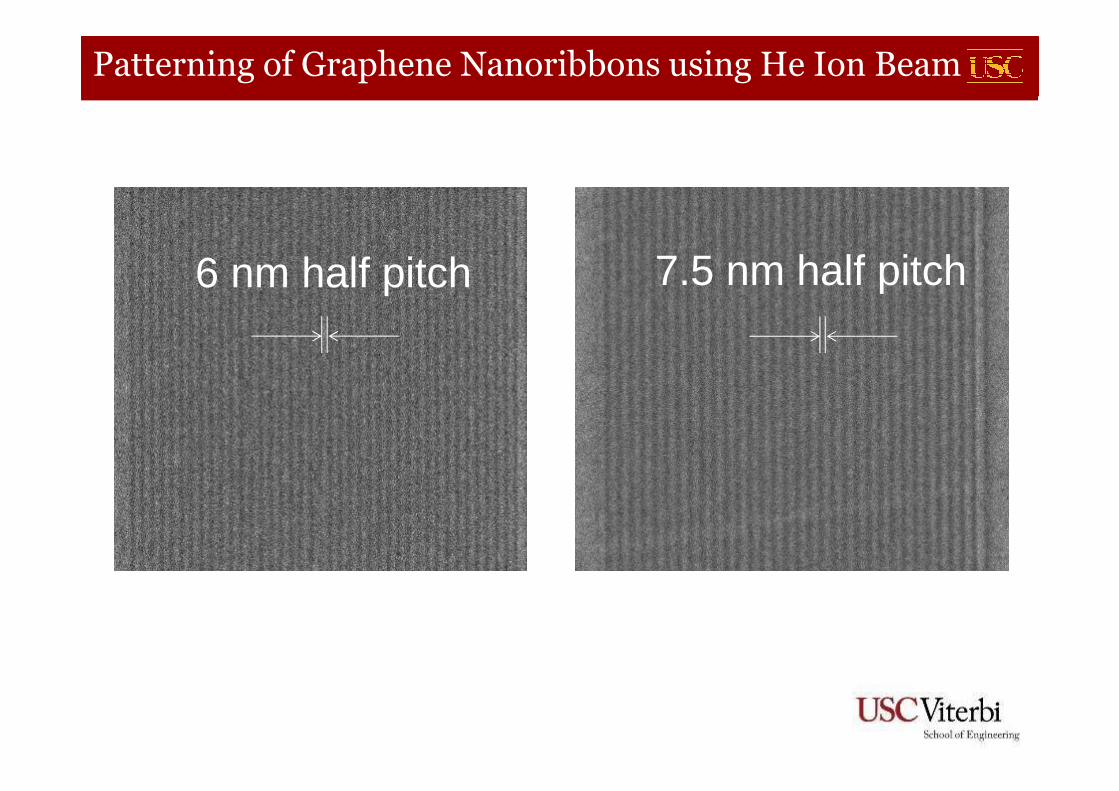
7.5 nm half pitch6 nm half pitch
Patterning of Graphene Nanoribbons using He Ion Beam
Benchmark Graphene Line-edge roughness with Raman Spectroscopy
How smooth are those line edges?• Beyond the resolution of SEM, HIM…• TEM? Maybe…• How about Raman spectroscopy?
A. C. Ferrari, J. C. Meyer, V. Scardaci, C. Casiraghi, M. Lazzeri, F. Mauri, S. Piscanec, D. Jiang, K. S. Novoselov, S. Roth and A. K. Geim, Phys. Rev. Lett. 97 (18), 187401 (2006).
10 nm half-pitch GNRs by He ion beam milling
• G: breathing mode• D: defect mode, mainly from edges• Rougher edges, more atoms on the edges, so higher D peak• Using IG/ID as benchmark of the smoothness of edges
15 nm half-pitch GNRs by He ion beam milling
Comparison: GNRs patterned by EBL
S. Ryu, J. Maultzsch, M. Y. Han, P. Kim and L. E. Brus, Acs Nano 5 (5), 4123-4130 (2011).
D
G
Higher IG/ID means smoother edges.
Benchmark Graphene Line-edge roughness with Raman Spectroscopy
Comparison with Reported Raman Spectra Shows Smoother Line Edges
EBL+O2 RIE
S. Ryu, J. Maultzsch, M. Y. Han, P. Kim and L. E. Brus, Acs Nano 5 (5), 4123-4130 (2011).
Unzipped SWCNT
X. Wang, Y. Ouyang, X. Li, H. Wang, J. Guo and H. Dai, Physical Review Letters 100(20), 206803 (2008).D. Wei, L. Xie, K. K. Lee, Z. Hu, S. Tan, W. Chen, C. H. Sow, K. Chen, Y. Liu and A. T. S. Wee, Nat Commun4, 1374 (2013).
Z. Pan, N. Liu, L. Fu and Z. Liu, Journal of the American Chemical Society 133(44), 17578-17581 (2011).
Wrinkle engineering
GNR MOSFET
GNRs
G
S D
Electrode
Electrode
Graphene
Vd = 0.1 V
The gate dielectric got damaged by He+ ion.
5 nm GNR Has a Bandgap of 88 meV
Vg = 0 V
diffe
rent
ial c
ondu
cta
nce
Vg = 0 V
EA = 44 meV
EG ≥ 2 EA = 88 meV
Gmin= G1e
−EA
KB
T
A. N. Abbas, G. Liu, B. Liu, L. Zhang, H. Liu, D. Ohlberg, W. Wu and C. Zhou, Acs Nano 8 (2), 1538-1546 (2014).
GNR FET as Gas Sensor
• NO2 acts as an electron attractor • bandgap opening provides higher
sensitivity• Edge states are more active site to
bond with NO2
• Safe level of NO2 is 0.2 ppm• Detection of 20 ppb NO2 has been
demonstrated
G
S D
Summary
• Sub-5 nm patterning using
• HIBL and
• NIL
• Direct He ion milling
• Patterning of GNRs
• Better line-edge roughness than reported results with Raman data.