A national laboratory of the U.S. Department of Energy Office of Energy Efficiency & Renewable Energy National Renewable Energy Laboratory Innovation for Our Energy Future Subcontract Report NREL/SR-520-40191 Large-Scale PV Module Manufacturing Using Ultra-Thin July 2006 Polycrystalline Silicon Solar Cells Final Subcontract Report 1 April 2002 — 28 February 2006 J. Wohlgemuth and M. Narayanan BP Solar Frederick, Maryland NREL is operated by Midwest Research Institute ● Battelle Contract No. DE-AC36-99-GO10337
Transcript
A national laboratory of the U.S. Department of Energy Office of Energy Efficiency & Renewable Energy
National Renewable Energy Laboratory Innovation for Our Energy Future
Final Subcontract Report 1 April 2002 — 28 February 2006
J. Wohlgemuth and M. Narayanan BP Solar Frederick, Maryland
NREL is operated by Midwest Research Institute Battelle Contract No. DE-AC36-99-GO10337
Large-Scale PV Module Manufacturing Using Ultra-Thin Polycrystalline Silicon Solar Cells
Final Subcontract Report 1 April 2002 — 28 February 2006 J. Wohlgemuth and M. Narayanan BP Solar Frederick, Maryland
NREL Technical Monitor: R.L. Mitchell Prepared under Subcontract No. ZDO-2-30628-03
Subcontract Report NREL/SR-520-40191 July 2006
National Renewable Energy Laboratory1617 Cole Boulevard, Golden, Colorado 80401-3393 303-275-3000 • www.nrel.gov
Operated for the U.S. Department of Energy Office of Energy Efficiency and Renewable Energy by Midwest Research Institute • Battelle
Contract No. DE-AC36-99-GO10337
This publication was reproduced from the best available copy submitted by the subcontractor and received no editorial review at NREL.
NOTICE
This report was prepared as an account of work sponsored by an agency of the United States government. Neither the United States government nor any agency thereof, nor any of their employees, makes any warranty, express or implied, or assumes any legal liability or responsibility for the accuracy, completeness, or usefulness of any information, apparatus, product, or process disclosed, or represents that its use would not infringe privately owned rights. Reference herein to any specific commercial product, process, or service by trade name, trademark, manufacturer, or otherwise does not necessarily constitute or imply its endorsement, recommendation, or favoring by the United States government or any agency thereof. The views and opinions of authors expressed herein do not necessarily state or reflect those of the United States government or any agency thereof.
Available electronically at http://www.osti.gov/bridge
Available for a processing fee to U.S. Department of Energy and its contractors, in paper, from:
U.S. Department of Energy Office of Scientific and Technical Information P.O. Box 62 Oak Ridge, TN 37831-0062 phone: 865.576.8401 fax: 865.576.5728 email: mailto:[email protected]
Available for sale to the public, in paper, from: U.S. Department of Commerce National Technical Information Service 5285 Port Royal Road Springfield, VA 22161 phone: 800.553.6847 fax: 703.605.6900 email: [email protected] online ordering: http://www.ntis.gov/ordering.htm
Printed on paper containing at least 50% wastepaper, including 20% postconsumer waste
PREFACE This Final Technical Progress Report covers the work performed by BP Solar International Inc. for the entire contract period April 1, 2002 to February 28, 2006 under DOE/NREL Subcontract # ZDO-2-30628-03 entitled "Large-Scale PV Module Manufacturing Using Ultra-thin Silicon Solar Cells". This is the Final Technical Report for this subcontract so it will cover all of the work over the subcontract period, but with special emphasis on the third phase from October 1, 2004 to February 28, 2006. The following personnel at BP Solar have contributed to the technical efforts covered in this report. Dinesh Amin Neil Placer Roger Clark Joseph Creager Danny Cunningham George Kelly Bonnie Kinsey Timothy Koval Mohan Narayanan Andy Nguyen Jean Posbic Bei Wu Jay Shaner Nathan Stoddard John Wohlgemuth Murray Bennett Jay Miller Steve Roncin BP Solar has been supported by subcontracts at the Automation and Robotics Research Institute at the University of Texas at Arlington (ARRI), at North Carolina State University (NCSU), the University Center of Excellence for Photovoltaic Research and Education at Georgia Institute of Technology and the Nanomaterials and Nanomanufacturing Research Center at the University of South Florida (USF). ARRI staff that worked on the subcontract included Heather Beardsley, Raul Fernandez and Brian Huff. Georgia Institute of Technology staff that work on the subcontract included Ajeet Rohatgi, Manav Sheoran and Ajay Upadhyaya. USF work on the subcontract was performed under the direction of Dr. Sergei Ostapenko. NCSU work during the first two Phases was performed under the direction of Professor Gerald Lucovsky. NCSU work during the last Phase was performed under the direction of Dr. George Rozgonyi.
iv
EXECUTIVE SUMMARY The major objectives of this program were to continue the advancement of BP Solar polycrystalline silicon manufacturing technology. The Program included work in the following areas.
• Efforts in the casting area to increase ingot size, improve ingot material quality, and improve handling of silicon feedstock as it is loaded into the casting stations.
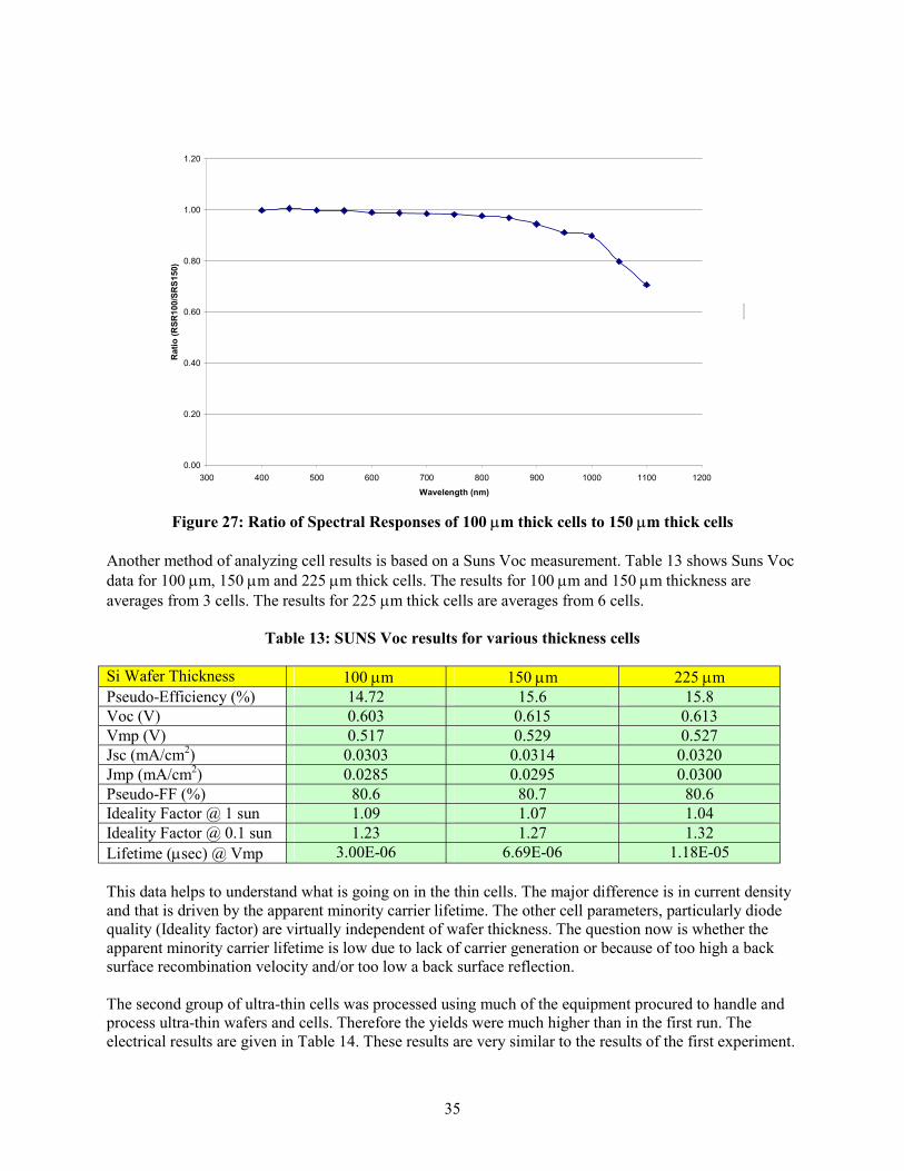
• Developing wire saws to slice 100 µm thick silicon wafers on 290 µm centers. • Developing equipment for demounting and subsequent handling of very thin silicon
wafers. • Developing cell processes using 100 µm thick silicon wafers that produce encapsulated
cells with efficiencies of at least 15.4% at an overall yield exceeding 95%. • Expanding existing in-line manufacturing data reporting systems to provide active
process control. • Establishing a 50 MW (annual nominal capacity) green-field Mega-plant factory model
template based on this new thin polycrystalline silicon technology. • Facilitating an increase in the silicon feedstock industry’s production capacity for lower-
cost solar grade silicon feedstock.
ACCOMPLISHMENTS There have been significant accomplishments during the course of the program including a number of developments that have been implemented in BP Solar production. Silicon feedstock BP Solar formed a strategic partnership and demonstrated good yields and cell efficiencies using cast solar grade silicon feedstock. The partner is now building a solar grade silicon pilot plant. Casting BP Solar demonstrated the casting of ingots > 300 kg, but due to production equipment limitations only increased the production ingot size from 240 kg to 265 kg; developed a method to reduce the amount of carbon in the cast silicon and have begun implementation; and expanded production capacity by adding the latest commercially available directional solidification equipment. Wafering BP Solar demonstrated the slicing of 125 µm thick silicon wafers; demonstrated the use of thinner wire (140 µm versus 160 µm); switched production from 250 µm thick wafers to 225 µm thick wafers; and demonstrated the ability to process 200 µm thick wafers in the production line. Wafer Demounting BP Solar identified a vendor of commercial wafer demounting equipment, procured the equipment and tested one unit. Wafer Handling ARRI built and BP Solar demonstrated belt to belt transfer of standard thickness and 100 µm thick cells.
v
Cell Process BP Solar identified and procured equipment to do in-line chemical etching; identified the process and procured the equipment for iso-chemical texturing; optimized the SiN process introduced during the first year of the program; evaluated and qualified hot melt front paste as an alternative for standard screen print paste and began implementation in production; and successfully processed 100 µm thick cells. Module Assembly BP Solar has eliminated lead from interconnect ribbons on all commercial multicrystalline products; implemented laminated-in protective bypass diodes in a number of commercial products; demonstrated a 2.4% increase in STC output power using AR coated glass, qualified the glass through environmental testing and implemented it on some product lines; developed, qualified and commercialized a new back sheet for most product lines; developed, qualified and implemented new junction boxes for all products; and demonstrated an IR process for tabbing, and stringing of ultra-thin solar cells; and built modules using 100 µm thick cells. Measurement and Control BP Solar improved the in-line measurement systems for physical measurements of bricks, monitoring of the diffusion process and testing the integrity of all by-pass diodes. USF utilized the resonance Ultrasonic Vibration method to detect cracks in wafers and cells in less than 10 seconds. Factory of the Future BP Solar identified all of the process and handling equipment for the next generation factory; purchased and evaluated the performance of all but one of the identified pieces. ARRI built a factor simulation model to assist BP Solar in designing future factories.
vi
TABLE OF CONTENTS
Section Page 1.0 Introduction...........................................................................................................1 2.0 Baseline Process....................................................................................................3 3.0 Program Efforts.....................................................................................................5 3.1 Silicon Feedstock Development ..................................................................5
3.2.2 C and O Content...............................................................................7 3.2.3 Process Control ................................................................................7 3.3 Thin Slicing of Silicon Wafers ....................................................................8 3.4 Wafer Demounting and Handling................................................................9
3.4.1 Wafer Demounting ..........................................................................9 3.4.2 Handling of Ultra-Thin Wafers......................................................13
3.4.3 Processing Bricks to Reduce the Subsequent Breakage ................21 3.5 Cell Process Development .........................................................................23
3.5.1 Modeling and Analysis of Ultra-thin Cells....................................23 3.5.2 Cell Process Development .............................................................28 3.5.3 Results of Ultra-thin Cell Processing.............................................33 3.6 Module Assembly ......................................................................................36 3.6.1 AR Coated Glass............................................................................36
3.6.2 Building Modules with Ultra-Thin Solar Cells..............................39 3.7 In-Line Process Control .............................................................................45 3.7.1 In-Line Measurements ...................................................................45 3.7.2 Crack Detection .............................................................................46
Figure Page 1. Lot Average Cell Efficiency for Standard and Test Silicon........................................ 5 2. Standard Ingot and Larger 320 kg Ingot...................................................................... 6 3. Melt Energy History.................................................................................................... 7 4. Thin Wafer Comb as it came off of the Wire Saw ...................................................... 9 5.a ARRI Wet Wafer Demounting Prototype .................................................................. 11 5.b ARRI Wet Wafer Demounting Prototype .................................................................. 11 6.a ATI Wet Wafer Cassetting Machine ......................................................................... 12 6.b Details of Wet Wafer Cassetting Machine ................................................................. 13 7. Different Thickness Wafers under Stress ................................................................... 14 8. Laval Nozzle Comparison .......................................................................................... 15 9. Comparison of Analytical Approximations for Air Levitation .................................. 16 10. Numerical Modeling of Velocity Streamlines............................................................ 17 11. Stationary Supersonic Structures in Air Levitation.................................................... 17 12. Modeled Relative Pressure Distribution in Air Levitation......................................... 18 13. Pressure Profile for Data Set 12—1.5mm Gap, 300 kPa Line Pressure..................... 18 14. Integrated Net Lifting Force as a Function of Radius Sorted by Gap Width ............. 19 15. Bi-Directional Motion with no Moving Parts ............................................................ 20 16. VC-BALT Prototype .................................................................................................. 20 17.a Impact of Changing Thickness on Voc for Different BSRV’s
for bulk lifetime 25 µS ............................................................................................... 25 17.b Impact of Changing Thickness on Voc for Different BSRV’s
for bulk lifetime 250 µS ............................................................................................. 25 18.a Impact of Changing Thickness on Isc for Different BSRV’s
for bulk lifetime of 25 µS........................................................................................... 26 18.b Impact of Changing Thickness on Isc for Different BSRV’s
for bulk lifetime of 250 µS......................................................................................... 26 19.a Impact of Changing Thickness on Efficiency for Different BSRV’s
for bulk lifetime of 25 µS........................................................................................... 26 19.b Impact of Changing Thickness on Efficiency for Different BSRV’s
for bulk lifetime of 250 µS......................................................................................... 27 20. Efficiency Dependence on Thickness for Varying Lifetime, BSRV and BSR .......... 28 21. NaOH versus Iso-Chemical Texture on Multicrystalline Silicon............................... 29 22 Pictures of Wafer Edges ............................................................................................. 30 23. Thin Cell Bowing with Al Paste Back ....................................................................... 30 24. Results of PC-1D Modeling of 100 Ohm/square Selective Emitter ........................... 32 25. Hot Melt (left) and Screen Print (right) Metallization................................................ 33 26. Relative Spectral Response of 100 µm and 150 µm Thick Cells ............................... 34 27. Ratio of Spectral Responses of 100 µm thick cells to 150 µm Thick Cells ............... 35 28. Distribution of Module Power from AR Glass Pilot Run. ......................................... 37 29. Insolation YR, AC Yield and Performance Ratio for Each String of the Array ........ 38 30. Matrix of 100 µm Thick Cells before Lamination ..................................................... 39 31. Matrix of 150 µm Thick Cells before Lamination ..................................................... 40 32. IR Scan of Module made with 100 µm cells .............................................................. 41 33. IR Scan of Module made with 150 µm cells .............................................................. 42 34. IR Scan of Second Module made with 100 µm Cells ............................................... 44 35. Brick Measurement System........................................................................................ 45
viii
36 Experimental Set-up for Resonance Ultrasonic Vibrations Measurements. .............. 47 37. Full Range Frequency Spectrum on Uncracked Multicrystalline Si Wafer ............... 48 38. RUV Results for a set of 18 Good Wafers and one Cracked Wafer........................... 49 39. Section of the Discrete-event Simulation Model Depicting Charge Preparation ....... 52 40. Section of the Discrete-event Simulation Model Depicting Casting.......................... 53 41. Section of the Discrete-event Simulation Model Depicting Mount Ingot Sizing....... 53 42. Section of the Discrete-event Simulation Model Depicting Mount Set Logic........... 54 43. Section of the Discrete-event Simulation Model Depicting Wire Sawing................. 55 44. Section of the Discrete-event Simulation Model Depicting Cell Production 1.......... 56 45. Section of the Discrete-event Simulation Model Depicting Cell Production 2.......... 56 46. Section of the Discrete-event Simulation Model Depicting Order Entry logic.......... 57 47. Section of the Discrete-event Simulation Model Depicting Module Assembly......... 58 48. Machine Statistics Output .......................................................................................... 59
LIST OF TABLES
Table Page 1. Cast Polycrystalline Silicon Process Sequence ........................................................... 3 2. Cell Results for Initial Solar Grade Si Experiment .......................................................... 5 3. Coated Wafer Breakage Results................................................................................. 22 4. Coated Wafer Chipping Experiment .......................................................................... 22 5. Coated Wafer Breakage on Pre-struck Wafers........................................................... 23 6. Parameters used in Cell Modelling............................................................................. 24 7. PC-1D Simulation Results showing Loss Mechanisms ............................................. 24 8. I-V Characteristics Comparing Planar with ICT Surface Preparation........................ 28 9. I-V Characteristics of the Modules made from Planar and ICT Cells........................ 28 10. Ultra-thin Wafers Processed Using rear SiN Passivation and Ag Paste Grid ............ 31 11. Cell Results of Selective Emitter Experiment ............................................................ 32 12. Cell Performance of Ultra-thin Cells.......................................................................... 34 13. SUNS Voc Results for Various Thickness Cells........................................................ 35 14. Cell Performance of second Ultra-thin Cell Experiment............................................ 36 15. Cell results from the AR Glass Pilot Run................................................................... 37 16. Results for Modules made with Ultra-thin Cells........................................................ 40 17. Results for Second Module made with Ultra-thin Cells............................................. 43 18. Equipment for Future Factories.................................................................................. 50 19. Handling Transfers in Megaplant............................................................................... 51
1
1.0 INTRODUCTION The goal of BP Solar’s Crystalline PV Manufacturing R&D Project is to improve the Polycrystalline Silicon manufacturing facility, to reduce cost, improve efficiency and increase production capacity. Key components of the program are:
• Increasing ingot size; • Improving ingot material quality; • Improving material handling; • Developing wire saws to slice 100 µm thick silicon wafers on 290 µm centers; • Developing equipment for demounting and subsequent handling of ultra-thin silicon wafers; • Developing cell processes using 100 µm thick silicon wafers that produce encapsulated cells with
efficiencies of at least 15.4% at an overall yield exceeding 95%; • Expanding existing in-line manufacturing data reporting systems to provide active process
control; • Establishing a 50 MW (annual nominal capacity) green-field MegaPlant factory model template
based on this new thin polycrystalline silicon technology; and • Facilitating an increase in the silicon feedstock industry’s production capacity for lower-cost solar
grade silicon feedstock These goals are to be achieved while improving the already high reliability of today’s crystalline silicon modules. Three major subcontractors supported BP Solar during the Phase 3 effort:
1. Automation and Robotics Research Institute (ARRI) of the University of Texas at Arlington assisted BP Solar in developing equipment for automated handling and demounting of ultra-thin wire saw wafers and assisted in development of a model for the MegaPlant
2. Georgia Institute of Technology (GIT) supported BP Solar in thin cell device modeling, bulk lifetime measurements and cell processing on wafers of varying thicknesses.
3. The Nanomaterials and Nanomanufacturing Research Center at the University of South Florida (USF) developed a non-contact method for detecting cracks and micro-cracks in wafers, cells and partially processed cells.
The baseline for this PV Manufacturing R&D program was the polycrystalline process and production line as it existed at the conclusion of BP Solar’s previous PVMaT Contract NREL # ZAX-8-17647-05 entitled “PVMAT Improvements in the BP Solar PV Module Manufacturing Technology”.1, 2 This baseline is described in more detail in Section 2.0. The rationale behind this program was to identify specific areas in the baseline process where improvements in handling, process control or the process itself could significantly reduce cost, increase efficiency and/or improve capacity. The realization that feedstock silicon is becoming an increasing larger percentage of the overall cost lead to the incorporation of efforts to significantly reduce wafer thickness and to work with selected silicon feedstock manufacturers to secure a source of solar specific lower-cost solar-grade silicon feedstock. BP Solar has identified two external vendors, who have provided large capacity casting stations for the expansion of the BP Solar Frederick casting facility. Material quality from these stations was shown to
2
be equivalent to that made in the BP Solar baseline stations. Efforts during this program have included increasing the ingot size and improving the material quality. Developments in wire saw technology focused on reducing wafer thickness in order to reduce cost and increase the number of wafers/cm of brick that can be cut, thereby reducing the amount of silicon necessary per watt of modules produced. Work on cell processing was designed to increase the average cell efficiency to 15.4% (at Standard Test Conditions) for ultra-thin wafers while improving process control and reducing the overall module manufacturing cost. Areas of investigation include passivated AR coating, edge isolation, surface texturing, and selective emitter diffusion. In addition, those processes that are not compatible with processing of ultra-thin cells have been identified and modified. Wafer and cell handling will become more critical as the thickness decreasing. ARRI has assisted BP Solar in identifying approaches to handling of ultra-thin wafers throughout the production line. Improved measurement and control during processing should lead to improved yields and higher average cell efficiency. Three specific areas in the plant have been identified, where additional inline measurements have been implemented in an effort to significantly improve control of the process. This is the final report of the contract. Progress during the first two phases of the contract were reported in two annual reports, “Large-Scale PV Module Manufacturing Using Ultra-thin Polycrystalline Silicon Solar Cells” First Annual Subcontract Report, December, 20033 and “Large-Scale PV Module Manufacturing Using Ultra-thin Polycrystalline Silicon Solar Cells” Second Annual Subcontract Report, January, 20054. A summary article on the progress through January, 2005 was published in the Proceedings of the 31st IEEE Photovoltaic Specialists Conference.5 Technical efforts will be discussed in detail in Section 3.0. This section will provide a summary of the activities during the first two phases of the program with emphasize on the results of the third phase.
3
2.0 BASELINE PROCESS BP Solar’s Crystalline Silicon Technology is based on use of cast polycrystalline silicon wafers. The process flow at the end of NREL Contract # ZAX-8-17647-05 is shown in Table 1.
Table 1 Cast Polycrystalline Silicon Process Sequence
Casting Of
240 Kg Brick Ingots
Wire Saw Wafering 270 µm thickness
Cell Process
All Print with Aluminum Back Surface Field (BSF) &
Plasma Enhanced Chemical Vapor Deposition (PECVD) Silicon Nitride (SiN) AR
Module Assembly Hot Bar Soldering for Tabbing and Stringing
Lamination
Fast Cure Ethylene Vinyl Acetate (EVA)
Finishing
The various segments of BP Solar’s module manufacturing process as practiced at the beginning of this PV Manufacturing R&D program are described below. Casting BP Solar has purchased directional solidification equipment specifically designed for photovoltaics. In this process, silicon feedstock is melted in a ceramic crucible and solidified into a large grained semi-crystalline silicon ingot. The size of the cast ingot yields 25 – 12.5 cm by 12.5 cm bricks. Wafering During the previous PVMaT Programs BP Solar developed wire saw technology for cutting large area polycrystalline wafers and improved the performance by reducing the wire saw pitch to 450 microns with no loss in downstream yield, by separating and recycling the components of the wire saw cutting slurry, and by re-tooling older saws to increase their capacity by 40%. Cell Process The cell process sequence is based on the use of Thick Film Paste (TFP) metallization, where a commercially available screen-printed silver paste is applied as the current carrying grid on the front of the solar cell. This process has been designed to be as cost effective as possible. The high temperature process steps include: diffusion, firing of the front and back print pastes and PECVD deposition of a SiN antireflective (AR) coating.
4
During the previous PVMaT Program, BP Solar developed the cost effective PECVD SiN process. This process has now been implemented on all BP Solar screen print production lines. Module Assembly The first part of the module assembly sequence is to solder two solder plated copper tabs onto the front of the solar cells. BP Solar uses automated hot bar soldering machines to perform the tabbing operation. Tabbed cells are then soldered into strings using hot bar soldering equipment developed in the previous PVMaT program. Module Lamination The module construction consists of a low iron, tempered glass superstrate, EVA encapsulant and a Tedlar back sheet. The lamination process, including the cure, is performed in a vacuum lamination system. Then the modules are trimmed and the leads are attached. Finally, every module is flash tested to determine its STC power output.
5
3.0 PROGRAM EFFORTS The following sections detail the progress made in each task during the program with particular emphasis on the last phase.
3.1 Silicon Feedstock Development In this task, BP Solar has worked with a strategic partner to develop a solar-specific lower-cost solar-grade silicon feedstock. Initial small scale experiments indicated that the solar grade silicon being developed by our partner could be mixed at a proportion of 25% without negatively impacting the resultant cell performance. Table 2 shows results from the initial set of laboratory experiments.
Table 2 Cell results for initial Solar Grade Si Experiment
Silicon Average Cell Efficiency
(%) Intrinsic 14.94 25% SoG 14.94
Based on these results, a larger trial was conducted using a 25% mix of solar grade silicon in standard production ingots. Figure 1 shows the results of two lots with 25% SoG Si plotted along with the standard production runs in the same time period. There was no statistical difference in yield or efficiency between the standard material and the samples with 25% SoG Si.
Figure 1: Lot Average Cell Efficiency for Standard and Test Silicon
Based in the encouraging results at 25% mix, our strategic partner continued work on improving the quality of the solar grade silicon material. During the course of Phase 3 of the program, the material quality continued to improve. In a progression of experiments the fraction of solar grade silicon was increased from 25% to 50%, from 50% to 75% and finally from 75% to 100%. In each case the material incorporating SoG Si was able to match the standard material in yield and cell efficiency.
6
Over 50,000 cells have been fabricated using solar grade feedstock at varying percentages in the ingots. The next step in the development is demonstration of a pilot facility for production of solar grade silicon. 3.2 Casting Development In this task, BP Solar investigated improvements in the casting process in order to increase ingot size, improve material quality and improve process control. Each will be discussed in the subsections below. 3.2.1 Ingot Size Increase BP Solar has designed and demonstrated a prototype casting station that can increase the cast ingot weight from the standard 240 kg to over 300 kg. The first extra large ingot was cast using 320 kg of Si feedstock. It resulted in an ingot with an average height of 28.8 cm as compared to the standard height of 21.9 cm. Figure 3 is a picture of a standard ingot and this taller ingot. Material from this ingot was utilized to produce solar cells with equivalent cell efficiencies to the standard size ingots.
Figure 2: Standard Ingot and Larger 320 kg Ingot
There are several factors that limit complete production conversion to larger ingot size. Portions of the current tool set used to size the ingots into bricks has a cut depth limitation, making complete conversion to larger ingot weights impossible without stranding capital assets The manufacturer of many of our casting stations has also recommended a “do not exceed” weight of 280 kg, due to current mechanical design constraints on the internal and external drive components. Finally the present mix of silicon feedstock that is available does not allow for packing of such large volumes of Si (> 300 kg) into the crucibles.
7
Therefore the larger >300 kg ingots could not be implemented in production. Instead the size was increased from 240 kg to 265 kg in all casting stations. Productivity efforts shifted from larger size to reduced cycle times.
3.2.2 Oxygen and Carbon Content The concentration of oxygen and carbon within the grown ingots has been measured using FTIR. In a typical ingot the carbon saturates (at 6-8ppma) at about half height. However the oxygen decreases with a maximum near the bottom < 10ppma dropping to ~ 1.5ppma at the top. Measurements on ingots cast with solar grade silicon indicate no change in the carbon or oxygen content. A new insulation package was designed in an effort to reduce the production of free carbon in the atmosphere by reducing dusting of carbon components within the furnace. This was accomplished through reduction of the number of pieces in the assembly, reduced exposure of carbon felt to the furnace, and over-coating of insulation components with graphite foil sheet. These changes consistently produced ingots with carbon content of ~ 1ppma throughout the entire ingot. Unfortunately there was no improvement in cell efficiency from the reduced carbon level. However, reduction in carbon does lead to a reduction in the number of and size of SiC inclusions in the ingot. Therefore the carbon reduction process is being implemented in order to increase wafering yield.
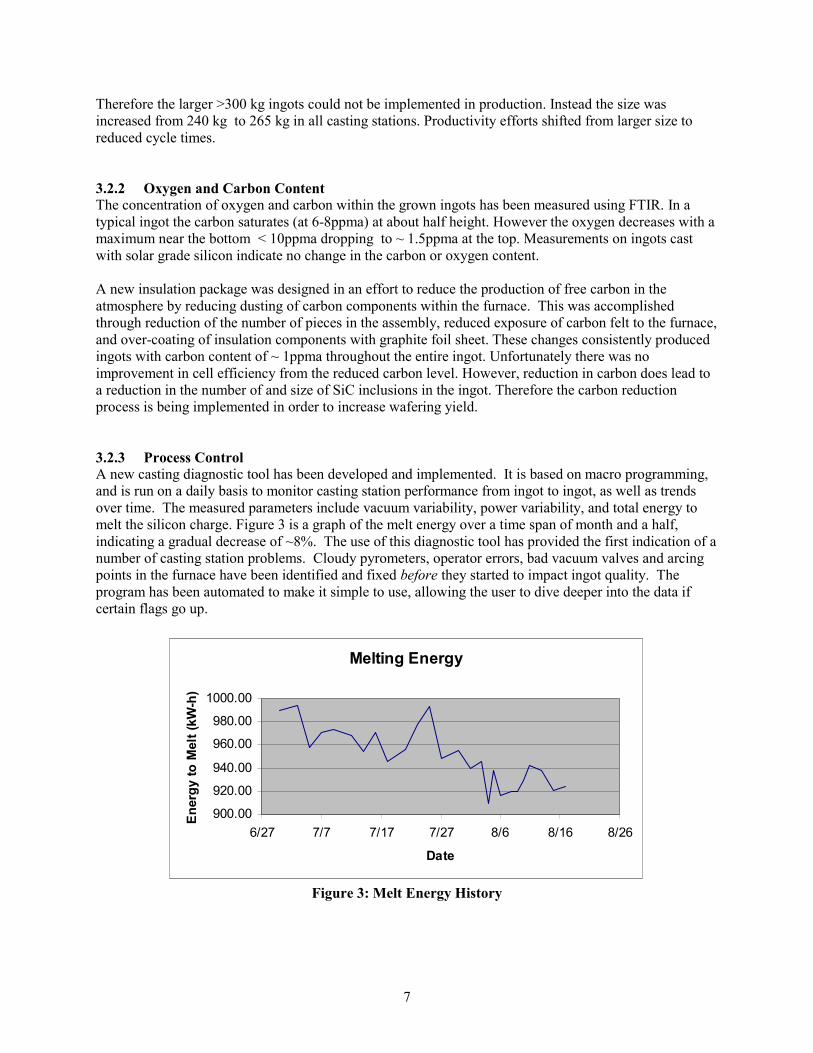
3.2.3 Process Control A new casting diagnostic tool has been developed and implemented. It is based on macro programming, and is run on a daily basis to monitor casting station performance from ingot to ingot, as well as trends over time. The measured parameters include vacuum variability, power variability, and total energy to melt the silicon charge. Figure 3 is a graph of the melt energy over a time span of month and a half, indicating a gradual decrease of ~8%. The use of this diagnostic tool has provided the first indication of a number of casting station problems. Cloudy pyrometers, operator errors, bad vacuum valves and arcing points in the furnace have been identified and fixed before they started to impact ingot quality. The program has been automated to make it simple to use, allowing the user to dive deeper into the data if certain flags go up.
Melting Energy
900.00
920.00
940.00
960.00
980.00
1000.00
6/27 7/7 7/17 7/27 8/6 8/16 8/26
Date
Ener
gy to
Mel
t (kW
-h)
Figure 3: Melt Energy History
8
3.3 Thin Slicing of Silicon Wafers In this task, BP Solar developed a process to slice silicon wafers of 100 µm thickness on 290 µm centers. A dual approach to sawing thinner wafers was utilized. One approach was to cut wafers that are somewhat thinner than the standard, which was 250 µm at the beginning of the period. The second approach was to leap frog to cutting 100 µm thick wafers. The first approach allowed for short term gains as well as providing valuable data on cutting and handling of marginally thinner wafers. The second approach would verify the potential to cut ultra-thin wafers as well as serving to identify those processes and handling steps that are not compatible with such ultra-thin wafers. Initially the first approach involved cutting 225 µm thick wafers rather than the standard 250 µm thick wafers. Many such runs were conducted with yields (all the way through to the module) and cell efficiencies similar to and ultimately equal to the yields achieved with the standard thickness wafers. This approach was so successful that BP Solar switched standard production to 225 µm during this period. Once the production line was stabilized on 225 µm wafers, experiments were conducted to evaluate going even thinner. A number of runs were conducted with 200 µm thick wafers as well as a few runs at 175 µm and 150 µm thickness. Over 6,000 200 µm thick runs were processed completely through the production line. The overall mechanical yield was reduced by approximately 5% while the average cell efficiency was unchanged. The added yield loss was about equally distributed over four process steps – diffusion, diffusion oxide removal, SiN deposition and metallization print/fire. Each of these areas was then evaluated to determine the specific mechanisms that were causing the additional breakage. The initial runs to cut 110 µm thick wafers were reasonably successful although a number of problems were identified. These included:
• Removal of the web from the brick required that the web be cut off and pulled out prior to wafer extraction.
• The glue edge has insufficient strength at 110 micron width to securely hold the wafers and overcome the friction drag of web extraction.
• Additional heat build-up because many more wafers are being cut at one time. • Need for increased drive power to cut the additional silicon. • Need for additional cooling and slurry heat removal
The first two issues were solved via engineering efforts at BP Solar. The last three issues must be addressed by improvements in the saws. As part of the program we worked with two wire saw manufacturers to address these issues via evaluating new equipment designed specifically to address these issues identified in the cutting of thinner wafers. Figure 4 is a picture of one brick wafered at 110 microns with a centimeter ruler adjacent. Only near the beam are all wafers able to be seen, as the surface tension of the cleaning agents causes them to stick together. Once out of the saw, the mounts required some special attention to handling. Initially breakage rates were high in demounting and cassetting if standard handling techniques and equipment were used. The efforts in the Wafer Demounting and Handling Task were extremely successful in identifying equipment and processes to allow the ultra-thin wafers to be demounted, cleaned and handled off to the cell process with high yields. These wafers have now being utilized for experiments in handling, as well as for developing of a cell process for ultra-thin wafers.
9
Figure 4: Thin Wafer Comb as it came off of the Wire Saw
The amount of silicon used per wafer and therefore per kilowatt of PV produced can be reduced by using thinner wafers and by cutting with thinner wire. Thinner wire (140 µm wire instead of the standard 160 µm) has been utilized to cut wafers on 290 µm centers, resulting in wafers that are approximately 125 µm in thickness. After subsequent processing these are reduced to 100 to 105 µm in thickness These run were performed using standard production conditions except for reduced loading. The wire cut very well with no apparent problems related to wire thickness. Through these tests and discussions with wire saw vendors, the realization was reached that a combination of large cutting volumes, thin wire, thin wafers, high yields, and low cycle times begins to follow the law of diminishing returns. One can select to optimize any three of the five, but no more. In the next five years, the wire saw process will reach the limits of its capability to deliver reduced incremental wafer costs due the physical dynamics and demand of materials. A clear path to break this limit is not evident through what is known of slicing processes today. 3.4 Wafer Demounting and Handling In this task, BP Solar developed processes and equipment for demounting and subsequent handling of very thin silicon wafers. 3.4.1 Wafer Demounting BP Solar has taken a two pronged approach to wafer demounting. One approach involved a subcontract effort at ARRI, where they have built a wet wafer demounting prototype. Most of this work was reported on in the Second Annual Report4. This work will be summarized in the section 3.4.1.1 below. The second approach involved work with vendors of automated equipment. This effort lead to the purchase of wafer demounting equipment for standard thickness wafers, that has been demonstrated to work with ultra-thin wafers. This effort will be discussed in section 3.4.1.2 below.
10
3.4.1.1 ARRI Wet Wafer Demounting Prototype The ARRI work on wet wafer demounting was described in detail in the second Annual Report of this contract4. ARRI investigated multiple methods for automated wet wafer demounting. The combination of vacuum / shearing has been consistently identified as the most promising for this particular scenario. ARRI built five generations of prototypes to achieve wet wafer coin stack demounting. The following items have been identified as most relevant to the success of the process:
• A special vacuum pump design is necessary to cope with minor fluid ingestion. Certain makes of pumps can be easily modified for operation in this environment by removal of a cleaning filter.
• The vacuum cup material found to be optimal in terms of friction (soft silicone) is also compromised by presence of solvent; contact with a solvent must be avoided or minimized by thorough rinsing with water to prevent warping and loss of sealing. However, contact with the wire saw slurry has no deleterious effect on this vacuum cup material.
• The maximum shearing speed between wafers is limited by the high interfacial traction forces present, to a point where a single manipulator will not be able to perform both the singulation and cassette placement functions fast enough. However, with a “hand-over” operation after peeling the wafer from the stack, it is possible to achieve cycle times comparable to human handling (between 2 and 3 seconds per wafer).
• It has been found necessary to have a counter-rotating brush for most effective separation of the wafers.
The Phase 1 prototype was successfully demonstrated with wafers that had been individually flushed with water and thus were free of solvent (vacuum held with no problems). Additional testing was performed with wafers soaked in slurry exactly as they come out of the wire saw machine (carefully demounted by hand). The intent was to see if the machine could singulate wafers that had not been exposed to solvent and that were heavily drenched in slurry. The prototype was successful in demounting under these conditions. Virtually no slurry ingestion into the vacuum system was observed, presumably due to the heavy viscosity of the fluid. Performance of the vacuum cups in peeling wafers from the stack was satisfactory; although the slurry might have lowered the traction from the vacuum cups, it also works to diminish interfacial frictional forces. ARRI identified and successfully completed upgrades to the wet wafer demount prototype developed during Phase I of this program. The modified prototype was designed to be used for testing with ultra-thin 12.5 mm wafers. The prototype is shown in Figures 5a and 5b. The concept of the device involves using actuator controlled vacuum cups to engage the top wafer of the stack. After the cups have adhered to the top wafer, they are actuated forward to a position clear of the stack. During this process there is a bond between the wafers due to the presence of the viscous slurry. This causes multiple wafers to cling together and move forward as one unit. To prevent this, a rotating brush is placed such that the underside of the singulated wafers contact the brush. The friction between the brush and the wafers forces all the wafers back onto the stack except for the top wafer which has been engaged by the vacuum cups. At this point the wafer is released and the vacuum cups are actuated back to the starting point. The wafer stack is indexed upward and the process is repeated. The singulator was evaluated versus its ability to operate under two conditions: the first involving slurry-coated wafers, and the second involving wafers that have undergone a solvent rinse. The first test using slurry-coated wafers did not perform as expected. The rotating brush could not provide enough counterforce to overcome the slurry-induced bond between the wafers. The downward displacement of the vacuum cups were increased and the wafers were more firmly pressed against the brush. This resulted in increased friction between the wafer and the brush, but wafers began to consistently fracture. The yield of intact wafers was very low.
11
The second test showed substantial improvement and promise. Due to the solvent rinse, the wafers did not adhere to each other as aggressively and could be separated by the wafer singulator. After adjusting the downward displacement of the vacuum cups, and reducing the vacuum pressure, the yield of intact wafers increased dramatically. Three runs were completed using this configuration. The only area of difficulty involved the upward indexing of the wafer stack. It did not properly compensate for the thickness of the thinner (175 µm) wafers and needed repeated adjustments. After proper tuning it is expected that this could be remedied.
Figure 5a: ARRI Wet Wafer Demounting Prototype
Figure 5b: ARRI Wet Wafer Demounting Prototype
While the ARRI prototype worked quite well the attempts to identify and qualify commercial equipment was successful (as described in section 3.4.1.2) so the ARRI approach was not commercialized.
12
3.4.1.2 Commercial Wafer Demounting Equipment BP Solar identified a commercial supplier of equipment designed to singulate and cassette or stack wafers after wire sawing. Automation Technology Inc. makes a wet wafer singulation (WWS) machine designed to de-stack and cassette wet silicon wafers. The operator removes wafers from a wire saw beam and loads a stack of wafers two (2) inches high into a magazine. The full magazine is then loaded into the coin-stack elevator. An empty cassette is then loaded into the cassette elevator. ATI’s specially designed end effector removes one wafer at a time from the coin-stack of wet wafers and transfers the wafer into the waiting cassette. Cassettes are indexed down until full. The initial trials were conducted at the vendor’s site. Wafers soaked in the standard cleaning solvent were fed into the ATI machine in stacks of about 100. The machine de-stacked and cassetted standard thickness wafers at a rate of 1 wafer every 2 seconds with a yield in excess of 99%. Wafers 175 µm thick were then fed into the machine. Once again these were de-stacked and cassetted at the same rate with virtually no breakage. Finally 125 µm thick wafers were de-stacked and cassetted. The ultra-thin wafers required mechanical adjustment before it would work correctly. Even then there was some breakage associated with handling the ultra-thin wafers. BP Solar purchased one of these machines from ATI. The machine is shown in Figure 6a and 6b.
Figure 6a. ATI Wet Wafer Cassetting Machine
13
Figure 6b: Details of Wet Wafer Cassetting Machine
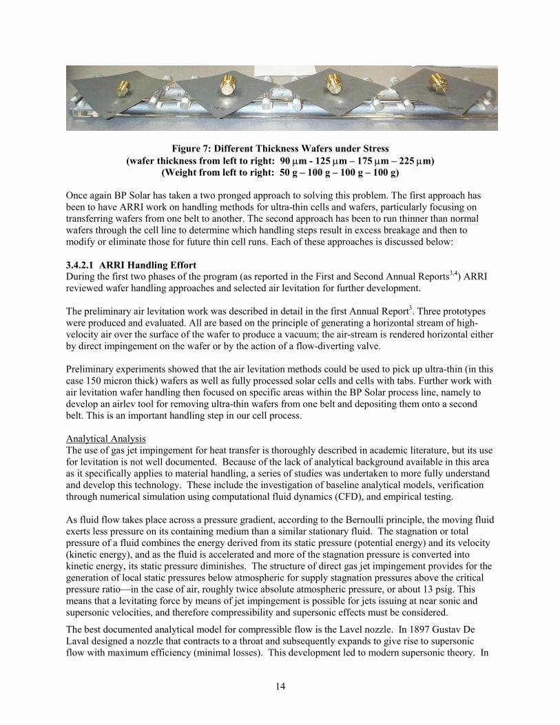
The wet wafer cassetting machine was installed in BP Solar facilities. A site acceptance test was then conducted to evaluate its performance. During the acceptance test, the machine ran at a throughput rate of 840 wafers/hour for 8 hours. There was almost no recordable breakage during the entire 8 hour acceptance test. There were several instances where multiple wafers were placed into the same cassette slot. Programming changes should eliminate the majority of these multiple feeds. Broken wafers in the input stack did not cause any problems for the machine. Subsequent small scale trials with thinner (175 µm) and ultra-thin (125 µm) wafers have been successfully run through the machine without significant yield loss. 3.4.2 Handling of Ultra-thin wafers Once ultra-thin wafers are demounted from the wire saw comb, they must be handled through the production line and ultimately incorporated into PV modules. Figure 7 shows how the flexibility of the silicon wafers varies as a function of thickness. Going from left to right in the figure, the wafers are 90 µm, 125 µm, 175 µm and 225 µm. The 90 µm wafer has a 50 gram weight on it. The other 3 wafers are loaded with a 100 gram weight.
14
Figure 7: Different Thickness Wafers under Stress (wafer thickness from left to right: 90 µm - 125 µm – 175 µm – 225 µm)
(Weight from left to right: 50 g – 100 g – 100 g – 100 g)
Once again BP Solar has taken a two pronged approach to solving this problem. The first approach has been to have ARRI work on handling methods for ultra-thin cells and wafers, particularly focusing on transferring wafers from one belt to another. The second approach has been to run thinner than normal wafers through the cell line to determine which handling steps result in excess breakage and then to modify or eliminate those for future thin cell runs. Each of these approaches is discussed below: 3.4.2.1 ARRI Handling Effort During the first two phases of the program (as reported in the First and Second Annual Reports3,4) ARRI reviewed wafer handling approaches and selected air levitation for further development. The preliminary air levitation work was described in detail in the first Annual Report3. Three prototypes were produced and evaluated. All are based on the principle of generating a horizontal stream of high-velocity air over the surface of the wafer to produce a vacuum; the air-stream is rendered horizontal either by direct impingement on the wafer or by the action of a flow-diverting valve. Preliminary experiments showed that the air levitation methods could be used to pick up ultra-thin (in this case 150 micron thick) wafers as well as fully processed solar cells and cells with tabs. Further work with air levitation wafer handling then focused on specific areas within the BP Solar process line, namely to develop an airlev tool for removing ultra-thin wafers from one belt and depositing them onto a second belt. This is an important handling step in our cell process. Analytical Analysis The use of gas jet impingement for heat transfer is thoroughly described in academic literature, but its use for levitation is not well documented. Because of the lack of analytical background available in this area as it specifically applies to material handling, a series of studies was undertaken to more fully understand and develop this technology. These include the investigation of baseline analytical models, verification through numerical simulation using computational fluid dynamics (CFD), and empirical testing. As fluid flow takes place across a pressure gradient, according to the Bernoulli principle, the moving fluid exerts less pressure on its containing medium than a similar stationary fluid. The stagnation or total pressure of a fluid combines the energy derived from its static pressure (potential energy) and its velocity (kinetic energy), and as the fluid is accelerated and more of the stagnation pressure is converted into kinetic energy, its static pressure diminishes. The structure of direct gas jet impingement provides for the generation of local static pressures below atmospheric for supply stagnation pressures above the critical pressure ratio—in the case of air, roughly twice absolute atmospheric pressure, or about 13 psig. This means that a levitating force by means of jet impingement is possible for jets issuing at near sonic and supersonic velocities, and therefore compressibility and supersonic effects must be considered.
The best documented analytical model for compressible flow is the Lavel nozzle. In 1897 Gustav De Laval designed a nozzle that contracts to a throat and subsequently expands to give rise to supersonic flow with maximum efficiency (minimal losses). This development led to modern supersonic theory. In
15
the conventional subsonic flow regime (converging nozzle), the fluid speeds up as it approaches the critical area (throat), reaching a maximum velocity of the speed of sound (Mach 1.0), whereupon it can progress to a supersonic regime during expansion (diverging nozzle) under prescribed downstream pressure conditions. The jet impingement device created in this project can be very roughly approximated by a double-throat Laval nozzle, where the impingement region performs the function of a secondary throat and also redirects the fluid to a horizontal direction. (See Figure 8)
Unfortunately, the actual flow patterns resulting from jet impingement upon a surface are complicated to the point where a detailed analytical model would be elusive and have limited predictive capability, as it would have to consider the effects of subsonic and supersonic flow regions, flow separation, wall jet shear layers, and interaction of normal and oblique shockwaves. For the practical development of impingement levitation devices, a complete understanding of these effects would be far beyond what is of interest for design purposes. However, while one must ultimately resort to numerical simulation or prototyping for detailed design and development, two highly simplified analytical models have been proposed.
Figure 8: Laval Nozzle Comaprison
The first model implements isentropic compression at the converging nozzle exactly as described in Laval nozzle theory. Assuming sonic conditions (choking at the throat), a coefficient of discharge is applied at the nozzle orifice as a ready means to reflect the observed reduction in stagnation pressure (it is duly noted that, in reality, such reduction in stagnation pressure in underexpanded (supersonic) jets is in fact due to the formation of a shockwave). This particular model applies all of the energy loss at the throat, and has a pressure discontinuity between the impingement region and the vacuum region. It is effective in estimating the peak vacuum and the impingement force, but does not fully explain the transition between impingement and diffuser regions. The second model also employs Laval nozzle theory of isentropic compression in the nozzle, but no discharge coefficient or other stagnation pressure loss is applied in this regime. Instead, loss of stagnation pressure is attributed to the disk diffuser region, and energy losses ahead of impingement are not considered in this flow regime (again, knowing that a significant stagnation loss does occur at high jet strengths). In a Laval nozzle there will be supersonic flow in the region of expanding area if the ratio of inlet and outlet pressure is sufficiently high. The fluid will continue to accelerate with expanding area until it begins to “back up” on itself. By attributing the energy loss to the supersonic diffuser, the second model better predicts the transition from impingement to vacuum, but overestimates the maximum vacuum achieved and the impingement force on the wafer.
16
The pressure profiles of the two models are shown in Figure 9.
Model 1
Energy loss at jet impingement Model 2
Energy loss in supersonic diffuser z Better at estimating peak vacuum z Better at estimating impingement force z Poor at predicting transition between
impingement and vacuum
z Overestimates maximum vacuum achieved z Overestimates impingement force z Better at predicting transition from
impingement to vacuum
Model 1 pressure distribution Model 2 pressure distribution
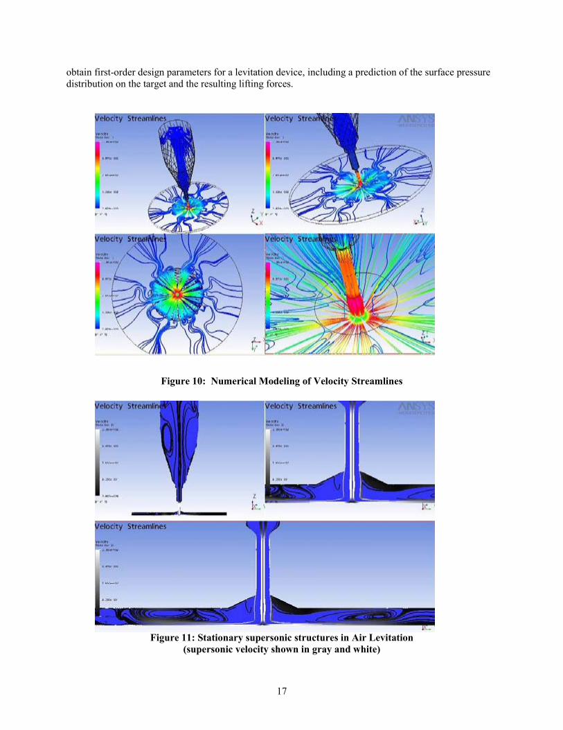
Figure 9: Comparison of Analytical Approximations for Air Levitation A more accurate analytical model would consider shockwave effects both ahead of impingement and at the flow redirection region, but the complexity intrinsic to the flow field makes the use of experimentally-correlated pressure loss factors inevitable. Ultimately practical considerations have a designer lean on numerical modeling rather than approximate analytical models to pursue the development of a specific levitation device. Computational Fluid Dynamic Analysis To further examine the impingement effects a numerical simulation was carried out using ANSYS CFX, a computational fluid dynamics (CFD) software package. This program allows the geometry to be created in a three-dimensional workspace to reflect the actual features of the problem, without simplification. The boundary conditions are specified (inlet and exit pressures, walls, symmetry, etc) and a finite element method is implemented to solve for the flow field variables. The CFX analysis was created using the geometry from the direct gas jet impingement end effector prototype of previous experiments. The CFX results are verified by the empirical testing of the actual prototype. The velocity streamlines are shown in Figure 10. The region of interest is the impingement region at the throat of the nozzle. The results of the simulation confirmed the presence of stationary supersonic structures, including a stationary shockwave and a large stationary eddy (see Figure 11). The CFX simulation confirmed that the most significant portion of vacuum happens within the jet impingement region, within a diameter of about one centimeter. This supports some aspects of the analytical approximation described in the previous section. In the pressure distribution shown in Figure 12, the area of high pressure in the center of the impingement area is shown in red, and the dark blue surrounding it reflects the vacuum region. In general, CFX simulation proves accurate and useful to
Po = 400 kPa abs Shockwave entered at Mach 3.3
Po = 400 kPa abs Cd = 0.4
17
obtain first-order design parameters for a levitation device, including a prediction of the surface pressure distribution on the target and the resulting lifting forces.
Figure 10: Numerical Modeling of Velocity Streamlines
Figure 11: Stationary supersonic structures in Air Levitation (supersonic velocity shown in gray and white)
18
Figure 12: Modeled Relative pressure distribution in Air Levitation
Empirical Testing In order to verify the CFX simulation and the analytical approximations, an experiment was setup for the direct gas jet impingement end effector to record the radial pressure distribution. An array of input pressures and gap distances were tested. The end effector was attached to the end of a robotic arm and the robot was programmed to slowly pass over a test plate with a small hole used as a pressure port. The end effector position was recorded by a displacement laser, and the pressure at the port was recorded through several electronic pressure sensors to provide the necessary range of pressure and vacuum. The test revealed the pressure profiles shown in Figure 13 for one particular gap and input pressure.
Figure 13: Pressure profile for data set 12—1.5mm gap, 300kPa line pressure
In the pressure profiles there is a region in the center of the impingement area of high pressure surrounded by a region of low pressure. The high pressure is an effect of the high velocity low pressure air impinging on the surface and recompressing. The low pressure area is the result of the recompressed air rushing outwards toward the outlet at high velocity. The high pressure present at the point of impingement (center of graph) is about six times the low pressure of the annular vacuum region, but the area with vacuum is much larger due to the radial configuration of the disk. To better visualize the effect, the pressure is integrated over the disk and the net force is calculated as shown below in Figures 14. The net force is positive (downward) close to the center but quickly drops to a negative (lifting) value at a radius of 5-7mm. The integration shows that the net force continues to increase beyond 10 mm but this is due to noise in the sensors and the exponentially increasing cylindrical area used in the integration of the force; in practice, lifting forces are minimal in near-sonic regimes.
19
Figure 14: Integrated net lifting force as a function of radius sorted by gap width
Directional Levitation Prototypes The original Directional Air Levitation Track (DALT) prototype delivered in Phase II introduced the concept of horizontal transfer levitation, and concentrated on proving the idea with a preliminary prototype. However, it had not completely addressed some of the important operational implementation issues; for example, it caused the wafers to travel with velocity too great for safe handling, and wafers would occasionally jam at the entrance of the track due to rotational misalignment upon wafer capture. During the third year of this research, a series of prototype developments was undertaken to refine the initial DALT design. The Velocity Profiled Directional Air Levitation Track (VP-DALT) was designed to remedy some of the known problems. This track shared the purpose and simplicity of the DALT, but attempted to reduce the speed at which wafers are discharged from the track while minimizing wafer misfeeds. After completing computational fluid dynamic analysis of the typical flow field in air jet impingement, it was discovered that the VP-DALT track face could be reduced, greatly simplifying its manufacture through the use of readily available aluminum extrusion sections. The narrow Velocity Profiled DALT (nVP-DALT) prototype was constructed based on this theory, and was ultimately delivered to BP Solar, complete with sensors and valve control for automatic operation. The DALT and the VP-DALT are both designed as one-way devices. It seemed useful to create a multidirectional device to give more freedom in wafer handling, as well as to investigate the potential for arbitrary position control of the target along the track. To this effect, additional design and prototyping effort was committed, and the first prototype to offer bidirectional motion became known as the Mechanically Driven Bidirectional Air Levitation Track (MD-BALT). This device uses an array of mechanically rotated air jets to accelerate and decelerate wafers along a linear axis of motion as desired. The MD-BALT was followed by the Valve Controlled Bidirectional Air Levitation Track (VC-BALT), which offers similar functionality with no moving parts (except the two valves). The VC-BALT
20
proportionally pressurizes two plenums of oppositely oriented jets to affect the desired horizontal component of motion. The VC-BALT relies on two side-by-side, individually-controlled plenums connected to stationary jets aligned in opposite directions, such that the horizontal acceleration imparted on the wafer is proportional to the net horizontal sum of the two jets. (See Figure 15.) Two high-flow servo valves throttling the air flow into the plenums are controlled by computer, which allows for variable motion control and programming. Test programs were developed to allow for continuous “panning” of the wafer from side to side, both at fast and slow speeds, as well as to arrest wafer motion at arbitrary positions along the track. Although the ability to stop the wafer arbitrarily along the track is still dependent upon the spacing of the jets, the fact that they are angled helps to mitigate lift loss when the jet impinges on the edge of the target.
Figure 16 shows a picture of the VC-BALT prototype. This unit was delivered to BP Solar where its operation has been demonstrated. Because of the low stress imparted by the air jets, the prototype works with both standard thickness wafers and cells as well as 100 µm ultra-thin wafers and cells with minimal breakage.
Figure 16: VC-BALT Prototype
Figure 15: Bi-Directional motion with no moving parts.
21
3.4.2.2 In House Handling Efforts During the first two years of the program a number of thinner than normal wafers were run though the cell line in order to identify possible problems. Some of the problems identified are:
• When placed in cassettes for cleaning and etching, thinner wafers tend to stick together after the wet processing. Because they are stuck together, the wafers do not rinse or dry correctly.
• Thinner wafers (175 and 200 µm), although weaker, are more flexible than 250 µm thick wafers. Some of the breakage appears to be more dependent on impact than on flexure.
• Some of the increased breakage of thin cells can be attributed to loaders and unloaders, which, though designed to be low impact, are in many cases slightly out of alignment.
• Carriers and cassettes are often slightly warped or distorted, resulting in wafer impact in situations where it should not occur.
• Conventional vacuum chuck depressions allowing manual (thumb and finger) pick-up have demonstrated wafer breakage with thin wafers.
After correcting a number of these issues, two pilot runs, each with about six thousand 225 µm thick wafers, were processed through the cell and assembly lines. The mechanical yields in both cases were comparable to standard mechanical yields in both cell and assembly lines. There was no significant difference in efficiencies.
Based on these results a larger trial of 225 µm wafers was conducted. Over 54,000 wafers ~ 225µm thick wafers were processed into cells and then into modules. Optimizing the line for the thinner wafers resulted in a 1.7% relative gain in average efficiency, but with a 0.5% increase in the number of electrical rejects due to increased shunts, probably caused by micro-cracks. Based on these results we slowly transitioned the entire production to 225 µm wafers. After running for several months the mechanical yield in sawing and wafer cleaning was 1.5% lower than for the 250 µm thick wafers. This means we cut and delivered about 4.5% more good thinner wafers to the cell line. In the cell and module areas the decrease in yield was between 0 and 0.5%. Overall use of the thinner cells increased our Watt/kg of silicon by about 4%. Once the production was stabilized on 225 µm thick wafers, experiments began with 200 µm thick wafers. In the initial run 15,000 wafers were produced, but with a 10% lower yield than for the 225 µm thick wafers. Lower mechanical yields occurred in the three main areas:
1. Demounting since this was done by hand at the time. Now that the ATI machine is in house this component should be reduced dramatically.
2. Stacking and unstacking of wafers. This practice will eventually be eliminated from the process sequence.
3. Cassettes in wet processing. A short term fix has been the redesign of the cassettes, but the long term solution is transitioning to in-line wet process steps.
3.4.3 Processing Bricks to Reduce the Subsequent Breakage One possible way to reduce wafer/cell breakage is to coat the silicon bricks prior to wafer sawing. This thin coatings could be effective for:
1) Sealing in existing damage (micro-cracks) 2) Preventing crack propagation 3) Preventing further edge damage during wafer handling steps 4) Improving wire saw yield
22
To test the extent of wafer strengthening, several tests were carried out. Care was taken to ensure that wafers sampled came from the same material. In general, a group of consecutive wafers was taken and sorted into two groups, one for coating and one uncoated for control. First, a set of wafers was edge-coated and their breakage forces were compared with a sister set from the same brick. The results are shown in Table 3. The average force to break a coated wafer was 20% higher than that required to break a standard non-coated wafer.
The second test involved striking the edge of a wafer in a controlled way to determine the force necessary to cause a chip in the edge of the wafer. The force is proportional to the height of the drop. The striking object was a metal edged ruler and the height is in increments of ½ inch. The results are given in Table 4.
Table 4: Coated Wafer Chipping Experiment Sample Coated Control Number Height to cause chip Height to cause chip
The third test involved first striking a wafer edge with a 1.5” ruler drop and then testing the bending force necessary to break the wafer. The results are shown in Table 5. The wafers coated on an edge prior to being struck had a higher average break force than even the control wafers from the first test (see Table 3) and about equivalent to the completely coated wafers in the first experiment.
23
Table 5: Coated Wafer Breakage on Pre-struck Wafers Sample Coated Control Number Break Force
These preliminary tests are very interesting as they have shown that wafers with edge coating:
1) Had 20% greater strength than uncoated control wafers 2) Had 50% better resistance to chipping 3) Were twice as strong as uncoated wafers after being struck with similar edge impacts.
3.5 Cell Process Development In this task, BP Solar worked on developing high efficiency cell processes for ultra-thin silicon wafers. The first part of this effort involved analysis and modeling to determine specific requirements imposed by the ultra-thin wafers. This will be discussed in section 3.5.1. Section 3.5.2 will present the efforts undertaken in process development to improve ultra-thin cell efficiencies. Finally the result of processing ultra-thin cells will be given in section 3.5.3 3.5.1 Modeling and Analysis of Ultra-thin Cells PC1D modeling6 of our present solar cells was undertaken in order to 1) better understand the limitations on our cells, 2) predict performance when using thinner wafers and 3) provide guidance for further efficiency enhancements. Real, measured or derived parameters were used wherever possible. In cases where no real data was available, approximations were made in order to yield the measured performance. Major parameters used in the model are:
• Cast multicrystalline silicon wafers • 225 µm thickness • 125 mm square cells (Area = 156.25 cm2) • Bulk Silicon Resistivity = 1 Ω-cm • Measured Nominal Cell Efficiency = 15.4% at STC (1000 Wm-2, 25 °C, AM1.5 spectrum) • Current Density = 33.0 mA/cm2 at STC • Open Circuit Voltage = 615.5 mV at STC
With the AM1.5 solar spectrum there are 3 fundamental loss mechanisms: 1. Long wavelength light that is not absorbed = 27.8% 2. High energy photons that produce hot carriers = 25.2% 3. Radiative and Auger losses = 17.2%
The result of these intrinsic losses is a fundamental limit efficiency of 29.8% for a crystalline silicon cell as shown in the “Ideal” column in Table 6. To evaluate the remainder of the loss mechanisms the parameters given in the “real” column of Table 6 have been utilized.
24
Table 6: Parameters used in Cell Modeling Item Ideal Real
Area (cm2) 156.25 143.25 Front Texture 3µm 1µm Back texture Planar textured
Front reflection 0 7.5% Front Internal Reflection 99/99 specular 75/92 diffuse Back Internal Reflection 99/99 specular 70/70 specular
The results of the step by step modeling are shown in Table 7. This table shows each of mechanisms that lead to a loss in cell efficiency. So the loss mechanisms that contribute the most to loss of cell efficiency are shadowing, front surface reflection, bulk lifetime, front surface recombination velocity and series resistance.
Table 7: PC-1D Simulation results showing Loss Mechanisms Losses Characteristic Isc Pmax Voc Eff Loss
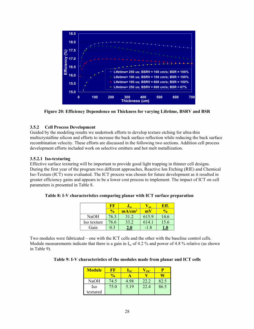
When we applied the model to different cell thicknesses, it gave virtually the same results regardless of wafer thickness from 300 µm down to 100 µm. This did not seem reasonable. BP Solar subcontracted Georgia Institute of Technology (GIT) to help us understand the behavior of ultra-thin multicrystalline solar cells through modeling and experimental device processing. GIT also used PC-1D to model cell performance. GIT provided sets of curves for two different bulk lifetimes (25 µS and 250 µS) that should span the range over which multicrystalline silicon will likely fall. For each of these lifetimes they provided plots of Voc versus cell thickness (Figure 17a and 17b), Jsc versus thickness (Figure 18a and 18b) and Cell Efficiency versus thickness (Figure 19a and 19b) for a range of back surface recombination velocities (BSRV). All of the curves are for a front surface recombination velocity (FSRV) of 45000cm/s and a back surface reflectance of 67%.
Figure 17a: Impact of Changing Thickness on Voc for Different BSRV’s for bulk lifetime of 25 µS
Figure 17b: Impact of Changing Thickness on Voc for Different BSRV’s for bulk lifetime of 250 µS
Figure 19b: Impact of Changing Thickness on Efficiency for Different BSRV’s for bulk lifetime of 250 µS
First looking at the curves for Voc we see that for low lifetime material 25 µS (where collection from deep in the bulk is not good) the voltage increases as the thickness decreases for all BSRV calculated. However, for the better lifetime material the voltage decreases with decreasing thickness for high BSRV, but increases with decreasing thickness for low BSRV (≤ 100 cm/s). For Jsc the story is similar. For low lifetime material (25 µS) the current collection is fairly insensitive to thickness for high BSRV (1000 cm/s), but increases with decreasing thickness down to about 100 µm thickness for lower BSRV. For high lifetime material (250 µS) the current collection decreases as the thickness decreases for all values of BSRV. For both cases below 100 µm in thickness the current density decreases dramatically as the incident sunlight is not absorbed in the Si. The efficiency curve for low lifetime material (25 µS) looks very similar to the curve for current collection. That is for low lifetime material the cell efficiency is higher at 100 µm thickness than for standard thickness (250 µm) for all BSRVs ≤ 1000 cm/s. On the other hand, for high lifetime material (250 µS) the efficiency is lower at 100 µm thickness than for standard thickness (250 µm) for all BSRVs, although the decrease is minimized for the lowest values of BSRV. So are we limited to always having lower cell efficiency at 100 µm thickness than at 250 µm when using high lifetime silicon? The answer is” no”, because we can improve the light absorption by improving the surface texture and increasing the back surface reflection (BSR), remembering that all of the above curves were calculated for a BSR of 67%. Figure 20 shows the efficiency versus thickness curve for 2 different combinations of BSR, BSRV and lifetime. The lowest curve represents what is most likely the present situation where thinner cells are less efficient. The good news from Figure 20 is that by using less than ideal material (lifetime of 100 µS) with improved BSRV (100 cm/s) and a BSR of 100%, a 100 µm thick cell can have an efficiency greater than 17.5%, significantly higher than the 16.5% achieved using the best material (lifetime of 250 µS) with today’s BSRV (600 cm/s) and today’s BSR of 67%.
Figure 20: Efficiency Dependence on Thickness for varying Lifetime, BSRV and BSR 3.5.2 Cell Process Development Guided by the modeling results we undertook efforts to develop texture etching for ultra-thin multicrystalline silicon and efforts to increase the back surface reflection while reducing the back surface recombination velocity. These efforts are discussed in the following two sections. Addition cell process development efforts included work on selective emitters and hot melt metallization. 3.5.2.1 Iso-texturing Effective surface texturing will be important to provide good light trapping in thinner cell designs. During the first year of the program two different approaches, Reactive Ion Etching (RIE) and Chemical Iso-Texture (ICT) were evaluated. The ICT process was chosen for future development as it resulted in greater efficiency gains and appears to be a lower cost process to implement. The impact of ICT on cell parameters is presented in Table 8.
Table 8: I-V characteristics comparing planar with ICT surface preparation
Gain 0.3 2.0 -1.8 1.0 Two modules were fabricated – one with the ICT cells and the other with the baseline control cells. Module measurements indicate that there is a gain in Isc of 4.2 % and power of 4.8 % relative (as shown in Table 9).
Table 9: I-V characteristics of the modules made from planar and ICT cells
During the second year of the program the development efforts included verification of the ICT process on larger groups of wafers and definition of the process specifications for implementation in manufacturing. Figure 21 shows the comparison of a NaOH etched multicrystalline wafer versus an iso-chemical textured wafer. These trials indicated that the ICT process interacted with a number of other processes in the fabrication sequence particularly the method used to clean the wafers after wire sawing and removal of the glue used to mount the brick during wire sawing. During the second year of the program these issues were addressed.
Figure 21: NaOH versus Iso-Chemical Texture on Multicrystalline Silicon
With the new cleaning procedures a number of additional ICT trials were completed. ICT continued to demonstrate a 250 mA short circuit current gain on 12.5 cm by 12.5 cm cells or approximately 5%. However, in many of the experiments there has been a loss in fill factor (~ 1.5 %) and a lower open circuit voltage (~ 3 mV). In addition to lower fill factor and voltage, there is a higher percentage of shunted cells, which we believe is due to problems in edge isolation. Loss in FF is mostly driven by lower shunt resistance possibly due to micro-cracks or junction etching during plasma junction isolation. Finally yields have been much lower with ICT processed cells because of high breakage rates. The saw damage on the wafer edge reacts with ICT, so pits are formed there as well as shown in Figure 22. These pits appear to be a source of micro-cracks that ultimately result in excess wafer breakage. While excess breakage continued to be a problem with ICT we were able to process several groups of cells that demonstrated the ability of the ICT to maintain current collection for ultra-thin cells. Use of ICT on 100 µm thick cells resulted in a 1.5% increase in short circuit current over the control, NaOh etched 250 µm thick cells.
30
Satisfactory implementation of ICT for ultra-thin cells requires:
• Improved treatment of brick edges before wire sawing. • Use of an in-line etch system for ICT processing. • Replacement of plasma etch as the junction isolation process.
Figure 22: Pictures of Wafer Edges
3.5.2.2 Back Surface Recombination Velocity BP Solar uses an aluminum paste back surface field (BSF) on it multicrystalline solar cells. There are two problems with use of Al paste on ultra-thin silicon solar cells.
1. Full back coverage of Al paste causes the cells to bow as shown in Figure 23. 2. The BSRV for Al paste BSF cells is typically in the range of 400 to 600 cm/s and the BSR is
typically around 75%7. The modeling indicates that these values will result in some efficiency loss with 100 µm thick cells. Figure 20 indicates that the Al paste BSF 100 µm cells should be about 1.7% absolute less (16% versus 17.7%) than a good back surface passivated cell.
Figure 23: Thin Cell Bowing with Al Paste Back
Standard Clean ICT Etch
31
Therefore an effort to develop passivated back contacts was initiated. Back Surface Passivation If most of the area of the back surface can be well passivated, high cell efficiency is possible. Since we already use PECVD SiN to passivate the front surface, it seemed logical to try using it to passivate the back with SiN and a fire through Ag paste grid (just like on the front). The passivated back was first evaluated using 115 µm thick wafers with both SiN and a screen printed silver grid on the back. No wafers were broken and there was no significant bow in the finished solar cells. The electrical results are shown in Table 10. None of these cells were particularly good. In all cases the fill factor was very low, the series resistance very high and the shunt resistance was low. As has been reported in the literature, while the charge on the SiN is the correct sign to assist on the front, this built in charge can result in parasitic shunting when utilized for surface passivation on the rear8.
Table 10: Ultra-thin Wafers Processed Using rear SiN Passivation and Ag Paste Grid
The other logical choice for back surface passivation is to grow a silicon oxide. However, our laboratory is presently not equipped to grow clean, undoped oxides so this was not an option for us. Low Bow Aluminum Paste So although modeling and preliminary experimental results suggest that an Al paste BSF is not the optimum back for ultra-thin cells, we had no other choice but to utilize this technology to fabricate ultra-thin cells during this program. Several paste vendors realized that bowing was a problem with their standard products and have developed aluminum pastes that are specifically formulated to reduce wafer bow after firing. These pastes were initially evaluated on standard thickness cells where they duplicated the performance of our standard aluminum pastes in terms of efficiency and yield. Modules made with these cells were then subjected to our internal qualification tests including 500 thermal cycles and 1250 hours of damp heat. The new low bow Al pastes passed all of the tests with minimal power loss. The low bow pastes were then evaluated using ultra-thin wafers. Breakage was not a problem during screen printing or firing, but a significant number of wafers suffered edge chips in the screen printing process. This necessitated a change in printer nest and handling procedure. The low bow pastes resulted in a 3 to 4 mm bow in the wafers about half of that observed with standard Al paste. All of the ultra-thin cell processing results presented in Section 3.5.3 were obtained using low bow Al pastes. 3.5.2.3 Selective Emitter A selective emitter refers to a process where a deeper diffusion is formed under the metallization to reduce series resistance and a shallower diffusion is formed in the collecting field to improve current collection. By decoupling the metallization diffusion from the field diffusion, higher cell efficiencies are expected. In the process under development at BP Solar, a dopant grid is printed with slightly wider screen openings than the front metallization pattern. This allowed for the front paste to be printed within
32
this lower sheet resistance selective emitter. The field emitter is then diffused with a much lower sheet resistance so the metal must stay within the deeper emitter to avoid shorting the junction. The results from one of the trials are given in Table 11. The selective emitter process resulted in an efficiency gain of 2.5%.
Table 11: Cell Results of Selective Emitter Experiment
Group Efficiency (%)
Isc (A)
Voc (mV)
FF (%)
Baseline 15.83 5.072 614.8 75.4 Selective Emitter 55 Ohm/sq field
16.21 5.019 621.4 77.3
Selective Emitter 65 Ohm/sq field
16.01 5.03 616.9 76.7
When implementing a selective emitter there is a desire to use a much lighter diffusion than has been successfully demonstrated. In our case use of emitters with sheet resistances above 65 Ohm/square have resulted in lower rather than higher cell efficiencies. Once again PC-1D modeling has been utilized to evaluate the performance of selective emitters. The modeling was carried out for a 100 Ohm/square selective emitter. Cell efficiencies were calculated for both multicrystalline and monocrystalline silicon over a range of front surface recombination velocities. The results are shown in Figure 24. The model clearly shows how important the front surface recombination velocity is for obtaining high efficiency when using a selective emitter with a high sheet resistance. Our standard 50 Ohm/square emitter yields an efficiency of approximately 15.5% for multi and 16.5% for mono, indicating an effective front surface recombination velocity of approximately 100,000 cm/sec. This is likely why we have been unsuccessful at increasing the efficiency using a higher sheet resistance selective emitter. Therefore our selective emitter efforts are now focusing on reducing the front surface recombination velocity in order to increase cell efficiencies.
Figure 24: Results of PC-1D Modeling of 100 Ohm/square Selective Emitter
3.5.2.4 Hot Melt Front Paste As part of this program we optimized, qualified and implemented hot melt front metallization to replace screen print. Hot melt has several advantages over screen print:
• Hot melt ink has the capability of printing taller and finer lines than screen printing. Figure 25 shows a comparison of screen print versus hot melt lines after firing.
• Hot melt ink solidifies immediately after the print, so can be processed and handled without the need to dry it in a furnace first as is required when using conventional wet inks.
Figure 25: Hot Melt (left) and Screen Print (right) Metallization
Initial work with the hot melt ink involved developing printing parameters and refining ink formulations, using the same firing conditions as used for the standard screen printed paste. The results indicate that this hot melt material performed very well at our standard production firing condition, easily besting the standard production material by between 1 and 2% in overall cell efficiency. This was based on improved FF and a higher Isc value. The Isc gain is driven by lower shadowing due to thinner grid lines. The FF improvement is driven by a combination of larger cross-sectional area in both the grid lines and bus bars, with the possible addition of a reduction in contact resistance between the fired ink and the emitter layer.
The next step was to optimize the firing using the hot melt paste. The best results for small lots were nearly 4% increase in efficiency above the screen print controls. However, as the process has now been transferred to the production line, the observed efficiency gain is 1.5 to 2%. BP Solar’s plan is to transition all production lines to hot melt paste during 2006. 3.5.3 Results of Ultra-thin Cell Processing Two major groups of ultra-thin cells have been fabricated during the third year of the program. In each case we co-processed 125 µm thick wafers and 175 µm thick wafers that became nominal 100 µm and 150 µm thick solar cells. Because of the problems with ICT resulting in low yields, the groups were processed with planar surfaces. All of these cells were processed using low bow Al paste BSF. In the first experiment the mechanical yield for the 100 µm thick cells was 82% and the electrical yield was 78% with most of the rejects being shunted cells. For the 150 µm thick cells the mechanical yield
34
was 92% and the electrical yield was 93% with only a few of the rejects being shunted cells. The electrical performance of the two groups is summarized in Table 12. The thinner cells clearly have lower efficiency than the thicker ones. All of the major cell parameters are lower for the thinner cells. The short circuit current of the thinner cells is 3% lower than the short circuit current of the 150 µm cells.
Table 12: Cell Performance of Ultra-thin Cells Wafer
Thickness Efficiency
(%) Isc (A)
Voc (mV)
150 µm 13.35 4.870 597.8 100 µm 12.20 4.724 587.9
To help understand if this difference is due to having less silicon to absorb the light, relative spectral response measurements were taken on 3 cells of each thickness. The results are shown in Figure 26. While the data does show clearly that the current collection loss is occurring at longer wavelengths, it is not obvious from this figure that absorption of light is the sole cause of lower current. To see this better, in Figure 27 we have plotted the ratio of the average relative spectral response for the three 100 µm thick cells divided by the average relative spectral response for the three 150 µm thick cells. This clearly shows that the reduction in spectral response for the ultra-thin cells is purely a function of wavelength. Use of surface texturing and improved back surface reflection are the best hopes for improving the collection of long wavelength light.
100u 337 w/ Light100u 408 w Light100u 409 w Light150u 105 w Light150u 121 w Light150u 221 w Light
Figure 26: Relative Spectral Response of 100 µm and 150 µm thick cells
35
0.00
0.20
0.40
0.60
0.80
1.00
1.20
300 400 500 600 700 800 900 1000 1100 1200
Wavelength (nm)
Rat
io (R
SR10
0/SR
S150
)
Figure 27: Ratio of Spectral Responses of 100 µm thick cells to 150 µm thick cells
Another method of analyzing cell results is based on a Suns Voc measurement. Table 13 shows Suns Voc data for 100 µm, 150 µm and 225 µm thick cells. The results for 100 µm and 150 µm thickness are averages from 3 cells. The results for 225 µm thick cells are averages from 6 cells.
Table 13: SUNS Voc results for various thickness cells
This data helps to understand what is going on in the thin cells. The major difference is in current density and that is driven by the apparent minority carrier lifetime. The other cell parameters, particularly diode quality (Ideality factor) are virtually independent of wafer thickness. The question now is whether the apparent minority carrier lifetime is low due to lack of carrier generation or because of too high a back surface recombination velocity and/or too low a back surface reflection. The second group of ultra-thin cells was processed using much of the equipment procured to handle and process ultra-thin wafers and cells. Therefore the yields were much higher than in the first run. The electrical results are given in Table 14. These results are very similar to the results of the first experiment.
36
Table 14: Cell Performance of second Ultra-thin Cell Experiment Wafer
These cell results support the modeling work that indicates the need for texture etching and probably the use of a different back surface passivation to achieve equivalent cell efficiencies with ultra-thin cells. 3.6 Module Assembly During this program a number of improvements have already been transferred to commercial production including:
1. AR coated glass has been implemented on one product line resulting in a 2.4% increase in average output power.9 Section 3.6.1 will discuss the AR coated glass effort in more detail.
2. A new back sheet with increased mechanical and dielectric strength is being incorporated into all BP Solar modules
3. Laminated by-pass diodes have been incorporated into a number of commercial modules. 4. New junction boxes have been developed for all module types. 5. All interconnect ribbons for screen print technology now use lead free solder.
The remainder of effort in this task was the development of and demonstration of module assembly processes and equipment suitable for use with ultra-thin solar cells. This effort is discussed in section 3.6.2. 3.6.1 AR Coated Glass The use of an anti-reflective coating on the outer glass surface can increase the coupling of light into a photovoltaic (PV) module and therefore increase its conversion efficiency. While AR coated glass has been available for years, in the past these coatings were unable to survive long term exposure outdoors. Recent advances in glass coating technology have improved the ability of the coatings to survive the outdoor environment. Previous work demonstrated module efficiency gains under standard test conditions (1000 W/m2 at normal incidence, AM1.5G spectrum, 25° C) of 2.4 to 3% when utilizing dip coated AR glass10. Sample modules were then deployed outdoors in Germany and Australia as part of BP Solar’s continuing outdoor test program11. The measured increase in energy was typically 4 to 6% (depending upon the time frame and location) versus the measured STC power gain of 2.5 to 3.0%. Modules made using the dip coated AR glass have been subjected to BP Solar’s extended version of the IEC 6121512 test sequence. The test sequence included exposure to 500 thermal cycles from -40 °C to +85 °C, 1250 hours of damp heat at 85 °C at 85% relative humidity and a combined leg of UV/50 thermal cycles and 10 humidity freeze cycles. The modules made with the AR coated glass successfully passed the qualification tests without any visual evidence of degradation of the coatings or power loss from the modules. In order to further evaluate the performance of AR coated glass a larger size pilot run was conducted. The AR and control modules built in the pilot run have been installed in two otherwise identical 41.5 kW
37
systems in Germany. The performance of the two systems has been monitored since April 1, 2005 to determine the energy production of each over an extended period of time. The pilot run included 231 AR coated glass modules and 231 control modules made with standard low iron glass. The modules were processed alternately (one AR and then one standard) in order to eliminate variability in the results. The results of the pilot run are given in Table 15. In this case the power improvement for the AR coated glass was 2.4% dominated by increased short circuit current as would be expected for AR coated glass. Figure 28 shows the distribution of module powers obtained during the pilot run. There is little overlap between the two distributions with the AR coating shifting all modules to higher power by approximately the same amount.
Table 15: Cell results from the AR glass pilot run
Glass Voc (V)
Isc (A)
Pmax (W)
Standard 44.1 5.42 179.5 AR 44.2 5.54 183.8 ∆ 0.2% 2.2% 2.4%
Figure 28: Distribution of module power from AR Glass pilot run
The pilot run modules have been installed on the roof of a building in Germany. The two arrays are tilted at 20°, oriented almost due south and suffer no shading. . Each array has 7 inverters with 3 by 11 modules feeding each inverter. The system controller takes measurements very 5 minutes of the following variables:
1. Date and time 2. Tilted Plane Irradiance from reference cell 3. Ambient Temperature 4. Module Temperature (one)
38
5. Wind Speed from anemometer 6. DC string voltage (42 substrings) 7. DC Power (42 substrings) 8. AC Power (14 strings)
From the data set we calculate Vdm (=Vdc/Vmax.stc), PF (DC Performance Factor), PR (AC Performance Ratio), YA (dc yield), and YF (ac yield) as functions of date/time, irradiance and temperature. By comparing the output of each of the strings over time we can determine how much additional energy the AR coated strings produce. Figure 29 shows the AC yield and performance ratio for each of the 14 inverters (each with 3 strings). Clearly the inverters with AR coated modules produced more energy during this time period. Summing the results for the whole time period, the array with AR coated modules produced 4.2% more energy than the array with the standard glass modules. This 4.2% gain should be compared to the 2.4% power increase measured at STC on the simulator. So the AR coating is more effective at reducing the amount of reflected light under conditions other than those used for the STC tests.
Figure 29: Insolation YR, AC Yield and Performance Ratio for each string of the Array
39
3.6.2 Building Modules with Ultra-thin Solar Cells The procedures for module assembly of nominal 100 µm thick solar cells were developed during the first two phases of the contract. The processing is described in the following sections. Tabbing and stringing- Front and back interconnect ribbons with lead free solder coating were soldered to the ultra thin cells using IR equipment. The standard liquid flux used in production was utilized. Strings were formed by attachment to successive cells. Layup - Conventional BP385 module components were used for the construction of the module. Glass and EVA were prepared and the individual strings of ultra thin cells were placed on the module layup Preassembled module bus bar sets from production were soldered in place into the end cells of the matrix using Teflon release paper to avoid damage to EVA. Conventional back EVA and backsheet were laid up on the assembled matrix without special precautions. Lamination - Lamination was carried out in a standard production laminator. The normal temperature for 36 cell modules with conventional cell thickness was used. A conventional lamination cycle of time and pressure was used. Termination – The laminate was trimmed with a hot knife and electrical termination was performed using the conventional burn through technique. Two 12 gauge Multicontact cables were soldered to the bus bars to terminate the module. Framing – The module was framed in the normal manner using hot melt butyl and the standard cross section Al frame. Modules from first batch of ultra-thin cells Cells from the first batch of experimental ultra-thin cells described in section 3.5.3 (See Table 12) were processed into two 36 cell modules, one using 100 µm thick cells and the other using 150 µm thick cells. Figure 30 shows the 100 µm cell matrix before lamination. Figure 31 shows the 150 µm cell matrix before lamination. Clearly there is a major difference in the degree of cell bowing.
Figure 30: Matrix of 100 µm thick cells before lamination
40
Figure 31: Matrix of 150 µm thick cells before lamination
The electrical performance of these two modules is presented in Table 16 along with the specification for this type of module based on standard thickness cells (225 µm). The module with 150 µm cells came close to matching the standard. Its parameters were consistent with the measurements on the cells that were used to make it. The module made with 100 µm cells had considerably lower performance with all parameters somewhat lower than typical standard modules. The current and voltage results are consistent with the measurements and analysis made on the 100 µm thick cells used to make it. However, the fill factor was lower by at least 2%.
Table 16: Results for Modules made with ultra-thin cells Parameter Specification for
BP380 Module with 150 µm cells
Module with 100 µm cells
Pmax (W) 80 76.3 67.8 Isc (A) 4.8 4.9 4.77
Voc (V) 22.1 21.8 21.5 FF(%) 75% 71.4% 66.3%
IR scans were performed to help determine why the fill factors were so low. The results for the module with 100 µm cells are shown in Figure 32. The dark patches in the picture are probably areas of cell that have been removed from the active circuit because of a crack in the silicon. The large number of hot spots in Figure 31 (especially those not associated with a solder bond) are likely due to cracks in the cells that result in shunts. Since low shunt cells and obviously cracked cells were excluded from use in module building, these are probably cells that were cracked during the tabbing/stringing operation. The results for the module with 150 µm cells are shown in Figure 33. There is much less structure in this picture, indicating fewer problems or cracks with the 150 µm cells. Based on the results for this module, a number improvements were developed for handling and processing the 100 µm thick cells through tabbing/stringing and matrix lay-up. These were implemented for fabrication of the module reported on in the next section.
41
Figure 32: IR scan of module made with 100 µm cells
42
Figure 33: IR scan of module made with 150 µm cells
43
Module from second batch of ultra-thin cells The 100 µm thick cells from the second batch of experimental ultra-thin cells described in section 3.5.3 (See Table 14) were processed into a 36 cell module. The revised procedures developed in response to the problems encountered with the first ultra-thin cell module were used in the fabrication of this module. The electrical performance of the modules are presented in Table 17 along with the specification for this type of module based on standard thickness cells (225 µm). This second module made with 100 µm cells still had considerably lower performance with all parameters somewhat lower than typical standard modules. However, now all of the parameters (current, voltage and fill factor) are consistent with the measurements and analysis made on the 100 µm thick cells used to make it. Figure 34 is an IR scan of this module. There is no indication of any cracked or shunted cells. So the process and handling changes implemented in tabbing/string and matrix assembly appear to have eliminated most of the cell damage previously observed in these steps.
Table 17: Results for Second Module made with ultra-thin cells Parameter Specification for
Figure 34: IR Scan of Second Module made with 100 µm Cells
45
3.7 In-Line Process Control In this task, BP Solar incorporated active feedback from manufacturing processes into the in-line measurement system at three specific places in the production line. These efforts are described in Section 3.7.1. BP Solar subcontracted with the University of South Florida (USF) to develop a crack detection system for multicrystalline silicon wafers and cells. The USF efforts are presented in Section 3.7.2 3.7.1 In-Line Measurements Three specific areas have been selected for implementation of active feedback into the production line. The three areas will be discussed below. Brick Measurements As part of QA procedures to maintain overall dimensional control for our multicrystalline wafer product, prior to wafering, the bricks of silicon are measured for both lateral size and orthogonal skew. This procedure has been done manually in the past requiring substantial handling and movement of bricks to complete the series of measurements with digital calipers and squareness tool with a dial indicator. In an attempt to reduce handling to facilitate increased production volume and increased brick size (weight), an inline, single-station measurement tool was designed, constructed, and implemented in production. The station utilizes five non-contact laser measurement heads, four long-range heads for dimensional check with a resolution of 10µm and a fifth for the orthogonal check with a resolution of 1µm. The heads are placed such that each measurement is opposed to a defining bearing surface that sets the zero surface. All five measurements are taken simultaneously and displayed at the proper precision to the operator on a readout panel. The display color has been set to display red for out of spec condition, yellow for marginal, and green for a pass condition. The displays are also capable of digital data output to allow for automatic data collection into our quality system. The system is shown in Figure 35.
Figure 35: Brick Measurement System
46
Monitoring of the Diffusion Process The second process selected for measurement and control improvements was diffusion. The control parameter for diffusion is the resultant sheet resistance of the diffused wafer’s surface. The sheet resistance is measured via a process called V/I measurement because that is actually what is measured before a sheet resistance is calculated. The V/I measurements have been taken for years. The improvement implemented under this program is to computerize the data. This was selected over automating the equipment because of the cost and complexity required for full automation. Having the data recorded by the computer minimizes operator error and operator problems where they just write down the same numbers every time. The new system requires the operator to select cells every hour from each of the diffusion furnaces. The operator places each of the cells under the 4 point probe at 9 selected locations. The computer saves the data and specifies whether each wafer is within specification or not. If not the operator and/or supervisor must take remedial action and remeasure 3 more cells. This helps to minimizes production of lower efficiency cells. Diode Integrity The standard flash test I-V curve will identify a shorted bypass diode. However, it will not tell whether the diode is operational nor whether it is actually electrically connected into the circuit. If the diodes are not installed or operating correctly any reverse current will have to flow through the cells. If this situation occurs in a high voltage system, a large voltage can be generated across a shadowed or damaged cell. These voltages are high enough to damage the cells and even to melt silicon, possibly causing a fire and ruining the module. To determine if the diode is installed and working properly, BP Solar has implemented a dark reverse current measurement of every module type manufactured with a bypass diode. If the diodes are installed and operating correctly the reverse current will flow through the diode when a small voltage is applied. If the diode is not operational or connected in the circuit, the reverse current must flow through the solar cells. Since solar cells have a high resistance in the reverse direction it will take a large implied voltage to get current flow. So the test procedure applies a small voltage in the reverse direction. If measurable current flows, the diode is operational and correctly installed. If the diode is not operational or connected correctly minimal current will flow and the tester will indicate a failure. This test procedure is now applied to all BP Solar modules manufactured with diodes. The test is performed before junction boxes and frames are attached. Therefore, if the module fails the test, the diode can be replaced and the module salvaged. 3.7.2 Crack Detection Wafer breakage during processing is a very high cost issue. This is particularly true when wafers fail during one of the print steps, generally resulting in several minutes of downtime while the operator cleans up the scattered parts and the wet paste. This is also a source of potential contamination. It is believed that wafers frequently fail at the print steps because they come into the process already cracked and the crack then fails when it is stressed during the process step. Wafer cracks can also cause electrical failure at cell or module test. University of South Florida has been subcontracted to help in developing a system for crack detection. In Phase 2 of the contract USF used a HS1000 HiSPEED™ Scanning Acoustic Microscope (SAM) by Sonix Inc. for surface morphology and structural (bulk) integrity evaluation. In SAM, a focused acoustic beam is scanned over the front and back surfaces of the wafer. The sound pulses are transmitted through the wafer and the reflection from the wafer interfaces is monitored. The ultrasonic pulses are generated by a high-frequency piezoelectric transducer. Electrical pulse from high voltage transmitter is converted to
47
mechanical energy. This activation causes the transducer to vibrate at a specific frequency causing ultrasonic pulses to be transmitted from the transducer. These pulses travel through the material at the material’s velocity and are reflected at the interfaces of the material it strikes. The ultrasonic energy does not travel well through air, so the wafers have to be placed in a coupling medium (deionized water bath). The system uses the pulse echo technique. The voltage data is then sent to the receiver and is amplified and digitized (providing peak amplitude and phase). SAM proved to be an accurate method for identifying cracks and micro-cracks in wafers and partially processed solar cells. In this case it provided BP Solar with information about where cracks and micro-cracks were first occurring and therefore has provide valuable information to assist in reducing breakage and increasing yield. However, each SAM wafer measurement took 20 minutes for sample set-up and data collection. This is clearly not an inline production process. The data from this effort was very useful as the sample set evaluated by SAM can now be used to calibrate and verify the accuracy of any new methods developed for crack detection. During the third phase of the program USF has been developing an Resonance Ultrasonic Vibrations (RUV) method as a rapid procedure to diagnose the mechanical quality of full-size Si wafers and solar cells. In the resonant ultrasonic method, ultrasonic vibrations of a tunable frequency and adjustable amplitude are applied to the entire silicon wafer as shown in Figure 36. The ultrasonic vibrations are generated in the wafer using a resonating piezoelectric transducer. The transducer contains a central hole which provides a reliable vacuum coupling between the wafer and transducer by applying a small (~ 50 kPa) negative pressure to the backside of the wafer. Ultrasonic vibrations are propagated into the wafer from the transducer and form standing acoustic waves at specific resonance frequencies. This vacuum method to couple the wafer and transducer allows fast wafer exchange and provides simple wafer alignment within 100 micron accuracy. The amplitude and spatial distribution of the standing waves are measured using a broad-band ultrasonic probe. In the present design, the ultrasonic probe measures the longitudinal vibration mode characteristics by contacting the edge of the wafer with controlled force. The resonance vibration system is computer controlled to achieve fast data acquisition and analyses. In this part of the project an elastic spring and a pressure sensor were added to the design in order to control the force on the probe-to-wafer contact with high accuracy.
Figure 36: Experimental set-up for resonance ultrasonic vibrations measurements.
48
In operation, the RUV system is utilized to make a full range frequency scan of the wafer. Figure 37 shows the full spectrum of the RUV scan made on one BP Solar 12.5 cm by 12.5 cm cast multicrystalline wafer. The insert shows the comparison with a single crystal silicon wafer of the same dimensions.
30000 40000 50000 60000 70000 80000 90000
0
5
10
15
20
25
55000 56000 57000 58000
0
1
2
3
~57KHzAco
ustic
am
plitu
de [m
V]
Frequency [Hz]
[mV]
frequency [Hz]
cast1 (BP) cz26a (Shell)
Figure 37: Full range frequency spectrum on uncracked multicrystalline Si wafer.
(The insert shows the 57 KHz peak compared to a similar Cz-Si wafer.)
USF has concentrated on using the resonance mode at about 57 KHz, which shows a reasonably narrow bandwidth of ~ 200Hz (Figure 37, insert). In a similar size Cz-Si wafer this peak is slightly shifted downwards and much narrower (~130Hz) as shown in the insert in Figure 37. Both effects can be attributed to higher internal stress in cast versus Cz material. One very important question was how uniform is the RUV signal obtained from multicrystalline silicon wafers. Figure 38 shows that the amplitude, frequency and bandwidth, all measured on a set of 18 cast wafers. Using multiple measurements the accuracy of peak position has been determined as +/- 10Hz, of BW as +/- 2 Hz, and amplitude as 10%. Wafer #11 has a 10 mm long crack introduced into it. As can be seen in Figure 38 the crack shifted the peak to lower frequency by 350 Hz, increased the peak bandwidth by 170 Hz and reduced the peak amplitude by 2.5 times. All three parameters are assessed within a single f-scan and can be used for fast identification of wafers with cracks. USF demonstrated the ability of the RUV system to determine whether a wafer had a crack or not in a 5 to 10 second test time.
49
Figure 38: RUV Results for a set of 18 Good Wafers and one Cracked Wafer 3.8 Megaplant Design In this task BP Solar was to develop a 50 MW (annual nominal capacity) green-field MegaPlant factory model template based on a new thin polycrystalline silicon product line. This template was to include the fully integrated, very thin wafer, high efficiency processes developed in the other tasks of this program, and was to be used for evaluating equipment and labor requirements as well as manufacturing costs. Since the concept of the 50 MW Megaplant was originally conceived as the final contract task, the commercial PV business has expanded dramatically. A 50 MW plant is no longer a Megaplant. Indeed the present factory in Frederick, Maryland has equivalent or larger production capacities for each of the 4 areas (casting, wafering, cell production, module assembly). So we already have a larger factory than was envisioned for the Megaplant. On the other hand, while a significant amount of work has been done on very thin or ultra-thin wafers and the standard thickness used in production has been reduced to 225 µm, BP Solar is not ready to implement ultra-thin wafers into manufacturing. Therefore, to make this task a meaningful exercise we have performed the following two efforts:
50
1. Specified all of the major pieces of equipment and the handling between those pieces of equipment for the processes developed in the other tasks. These efforts will be described in Section 3.8.1.
2. Subcontracted ARRI to develop a model of a large factory that could be used to design and model the performance of future factories. This effort will be described in Section 3.8.1.
3.8.1 Equipment Identification Once the processes had been selected for the various steps we began a search for equipment that was capable of performing the required procedures. Table 18 gives a list of each process and the type of equipment proposed for BP Solar future factories.
Table 18: Equipment for Future Factories
Process Type of Equipment Ingot Casting Directional Solidification
Sizing Band Saw Wafering Wire Saws
Wafer Removal from Saw Comb Hot water soak Singulation Wet wafer destacker
Front Metal Print Rotary Printer Back Metal Print Rotary Printer Metallization Fire IR Belt
Cell Test Xenon Lamp Tabbing/Stringing IR matrixing
Lamination Auto Laminators Final Test Single Pulse Xenon Simulators
BP Solar has purchased or built at least one of each type of equipment on the list except the in-line wafer cleaning. Such units have only recently become commercially available. Most of the units are already being used in production. The exceptions are the Singulation equipment (the wet wafer destacker) and the in line wet etch iso-chemical texturing unit. Both of these are still going through start-up validation in the technology area. By operating the specific pieces of equipment for each process step we are able to collect valuable date on process variability, yields, maintenance requirements, up-time and cost of ownership. This information has been extremely important for designing for future expansions. In addition to the equipment itself, we have also developed a long term plan for how to handle ultra-thin wafers and cells through the proposed factory. Table 19 provides a summary of how the ultra-thin wafers and cells would be transported through the production line.
51
Table 19: Handling Transfers in Megaplant
From Process Handling To Process Wire Saw → in combs → Comb Cleaning Glue softening → Special equip → Singulation Singulation → belt to belt → Wafer Cleaning Wafer cleaning → belt to belt → Inspection Inspection → belt to belt → Wet Etch 1 Wet Etch 1 → belt to belt → Diffusion Diffusion → belt to belt → Wet Etch 2 Wet Etch 2 → belt to platen → Si N Deposition SiN Deposition → platen to stack → Print Print → part of printer → Fire Fire → belt to belt → Cell Test Cell Test → load / pack → Tabbing/stringing or ship
3.8.2 Factory Model ARRI supported BP Solar in this activity by building the model. 3.8.2.1 ARRI Model Building The objective of this effort was to develop a decision support tool that aids the economic justification of ultra-thin photovoltaic (PV) cell production and other capital investments. This decision support tool consists of a discrete-event simulation model and supporting data entry forms that feed information to the model. This dynamic model of a PV module production facility encompasses the entire span of casting operations, wafer cutting, cell production, and module assembly. This tool can be used to model the impact on production of adding additional resources to the system or of creating a whole new production line (say for operation with ultra-thin cells). The model can be used to predict production rates, work in process levels, and delays in the completion of orders. Sensitivity models can also be constructed for the impact of cell breakage rates on product production. The simulation model was constructed within the Witness® discrete-event simulation package. An AutoCad® DXF file depicting the layout of the BP Solar Frederick facility was used as a backdrop for the Witness® simulation elements. The model can be logically decomposed into eight subsystems each representing a logical or physical component of the Frederick production operations:
• Silicon Charge Preparation Area • Casting Area • Ingot Sizing
52
• Mount Set Logic • Wire Saw Area • Cell Production • Order Entry Logic • Module Assembly
A brief description of functionality contained in each of these subsystems is provided below along with a figure depicting that area within the model. Charge Preparation Area - This component of the model depicts two sets of activities that contribute to the production of charges ready for processing in the casting area (figure 39). The first set of activities are associated with the preparation of the crucibles. The second component contained within this area depicts the cleaning of the silicon feedstock. These two components are integrated in the charge assembly area. We make the assumption in the model that the crucibles and silicon are always available.
Figure 39: Section of the Discrete-event Simulation Model Depicting Charge Preparation Casting Area – This area contains the casting stations used to form the ingots. The casting stations pull charges from a buffer conveyor. (See figure 40). Once the casting stations complete their cycle, the newly formed ingots are placed in a high temperature cooling rack (represented by a time buffer). After an initial cooling period the ingots are placed in a low-temperature cooling buffer where they wait until needed in the sizing saw area. Ingot Sizing – Once the ingots have been formed, they must be cut into bricks that correspond to the desired wafer size. The size of bricks to be cut is determined as a function of the mix of cell sizes requested by the user in the data entry spreadsheets. A random probability function is used to determine the size of the bricks to be cut from a specific ingot. After completing the simulated sizing saw processing time the saw element generates either 16 or 25 bricks of a specific size. These bricks are then passed to an inspection simulation element where they are assigned a “useful length” value. See Figure 41.
53
Figure 40: Section of the Discrete-event Simulation Model Depicting Casting
Figure 41: Section of the Discrete-event Simulation Model Depicting Ingot Sizing
54
Mount Set Logic – This model subsystem is designed to model the logic and tasks required to: a) Determine the type of mount sets that should be assembled next to balance wafer production in
accordance to the wafer type ratios assigned within the input spreadsheets. b) Search through the blocks of a given size to determine if a mount set of sufficient quality can be
assembled. c) Based on the number of bricks used to create the mount set, calculate the trim saw time required
to make the mount set. d) Delay the mount set entity for the time required to cut and mount the bricks onto the mount sub-
straights. e) Place the assembled mount set into one of four buffers designed to hold mount sets to be
processed by a specific class of wire saw. This area of the model attempts to model decisions made by human operators. The allocation of bricks to mount sets is based on the yield of the usable mount length. The mount set is assembled by pulling bricks out of a buffer containing bricks of a specific size. Bricks are taken from the front of the buffer until the selected brick exceeds the allowable mount length sum. At this point, the algorithm will search the queue looking for a brick that would fit within the remaining space in that mount set. This process is continued until all of the bricks in the queue have been evaluated. The quality of the mount set is then assessed. A ratio of the actual usable mount length over the theoretical maximum mount length is calculated. This value is compared to a minimum acceptable yield value. If the minimum yield requirement has been met, the block simulation elements are assembled into a single mount set entity that carries attributes that indicate brick type, theoretical mount length, and actual mount length. If the minimum acceptable yield value target is not reached, all of the bricks in the mount set are placed at the end of the brick queues. See Figure 42.
Figure 42: Section of the Discrete-event Simulation Model Depicting Mount Set Logic
Wire Saw Area – Four different sets of wire saws were modeled each with a different number of mounts and maximum length of usable material per mount set. Each saw pushes the completed mount sets into a
55
dedicated soak tank machine. A “tank token” entity is created for the mount set. This token is sent to a timed buffer where the token is forced to wait an adequate time before being made available for wafer singulation. A random function was used to determine if the mount set will be sent to in-house wafer singulation or will be assigned to the export singulation area. All exported wafers pass through a cleaning process and are then packaged for transport. The remainder of the mount sets are sent to “in-house” wafer singulation. See Figure 43.
Figure 43: Section of the Discrete-event Simulation Model Depicting Wire Sawing
Cell Production – The cell production area consists of all the processes required to convert a wafer into a solar cell. Within the simulation model this series of activities starts with “in-house” wafer singulation and ends with a cell grading process where the completed cells are classified by their efficiency ratings (See Figure 44 and 45). The model will collect and release batches of 1200 cells at a time through the cell production area. Throughout the cell production area the batch is broken up into smaller processing quantities like cassettes, coin stacks and individual wafers to meet the specific requirements of the processing equipment. The last process in the cell production is a cell grading process. Historical cell allocation ratios for each bin type were obtained from BP Solar. These ratios, indicating the relative frequency that each grade of cell is produced, are used to probabilistically assign each completed cell to a cell grade bin. A buffer element has been created for each bin. These cell bin buffers hold the cells that are “on-hand” to support Module Assembly.
56
Figure 44: Section of the Discrete-event Simulation Model Depicting Cell Production 1.
Figure 45: Section of the Discrete-event Simulation Model Depicting Cell Production 2
Order Entry Logic – The function of this component is to allow different module order schedules to be submitted to the model. These production orders are encoded within an external text file. The order entry
57
logic reads each production order from the text file at a predetermined time within the simulation run. The current production order data set is based on one year of production orders submitted to the module assembly lines between January 2005 to December 2005. The order entry logic is designed to support first-in, first-out logic so that larger orders are not superseded by smaller orders submitted later in the simulation run. The simulation contains separate buffers for orders requiring different bin classes. For each cell / bin combination a variable has been defined that determines if the orders will use “Startup Cells” or will require that the model produce simulated cells to fulfill the needs of the complete order. Without this mechanism, orders would have to wait until the model produced all the cells of a specific cell size and bin type for each order. Because of the stochastic nature of the cell production process and the fact that the model starts empty, there could be an extended period of time required to build the inventories for a specific cell size / bin combination at the beginning of the simulation. The order production schedule assumes that the orders are being released to a continuously operating facility. Without these special startup conditions, orders would simply queue until the cells were available in the completed cell bins. Once this back-log of orders is created, it would persist through the simulation run. Within the model, orders are released once a week. This is accomplished by assigning an arrival time for each production order element in the external order data file. Once a week in simulation time, any orders scheduled for release would be pushed into the model. These orders are sorted by cell type and bin into first-in, first-out buffers for that specific cell type / bin. The order release mechanism checks each of these order buffers in a round-robin fashion to ensure that all order types are given equal evaluation. The order release mechanism will take the first order out of each buffer. The order release mechanism will first determine if the “on-hand inventory” buffers contain enough cells of a specific type / bin to complete the order. If not, the “startup” flag for the order buffer will be checked. If it has been cleared then the order must wait until the simulation produces sufficient cells to fill the order. Under these conditions, the production order will be returned to the front of its respective order buffer where it will be re-evaluated after all the other order buffers have been checked. All orders requiring the same cell type / bin will have to wait until this order can be completed before being evaluated for release. See Figure 46.
Figure 46: Section of the Discrete-event Simulation Model Depicting Order Entry logic
58
Module Assembly – The module assembly area represented in the model consists of two parallel assembly lines. These lines are driven by the materials that are released to them. This material release process is performed by the order entry logic described above. This subsystem has two main sets of inputs: cells and glass. The number of cells required to complete a production order is calculated by the order release module. These cells are queued up in front of the tabbing stations on each line. Once tabbed, the cells are held in a series of buffers until they are assembled into strings of cells by the stringer. The glass that is queued in front of the glass wash station determines the modules that will be produced on the line. In the model, the actual module type and cell count is determined by the attributes that are carried on each glass entity. These attributes indicate the type and quantity of cells that need to be pulled from the tabbed cell buffers and assembled into a module. See Figure 47. It is possible to write a set of attribute values to an external data file each time a module is packaged and exits the model. For each module produced we can calculate the elapsed time between when the production order entered the model and when a particular module assembled to fulfill that order was packaged for shipping. This elapsed time and the production order queuing statistics can be used to determine if the modeled facility can keep up with projected levels of demand.
Figure 47: Section of the Discrete-event Simulation Model Depicting Module Assembly
Model Data Input - A secondary objective was to develop a maintainable tool that can be used with minimal knowledge of discrete-event simulation and proprietary simulation software languages. To support this objective a set of external data input tools were developed to drive the model. Under this strategy, the internal structure of the model is specific to a given production facility but system resource levels, cycle times, and unit resource costs can be specified through a series of external tools like Excel® worksheets. Additional user defined probability distribution functions were defined within the Witness tool to accurately model the variability present in the system.
59
The major input data sets that drive the model are: • Production Ratios and Equipment Performance Excel ® worksheets • Equipment Allowance Excel ® worksheets. • A production work order data file. • Custom Distributions defined within the Witness Model.
Model Output - The standard statistical output generated at the end of each simulation run can be used to obtain a wide range of system performance characteristics. Machine utilization data is particularly useful in identifying bottleneck resources in the system (figure 48). Part statistics will indicate the number of units complete, scrapped, as well as current and average work in process levels. In addition to the standard reports generated at the completion of each run, the Witness tool supports the generation of custom reporting mechanisms. These custom reporting mechanisms are used to generate a log file indicating the amount of time required to fill each module production order. The graphical representation of the facility is also helpful to observe system dynamics. It is important to note that this is a very large model and in graphical mode, the simulation runs very slowly. Graphics can be turned off to fast-forward the model.
Figure 48: Machine Statistics Output
3.8.2.2 Use of the Model The model was constructed such that one primary input sheet can be adjusted to reflect equipment mean time before failure (MTBF), mean time to repair (MTTR), setup and changeover allowances. Another input sheet accepts finished module demand schedule, and in the case of the test simulations, actual plant demand was used as a validity check. Wafer size selection and cell efficiency distributions are deterministic, a set percentage is assigned to reflect either running averages or can be set higher or lower to mimic a specific process or demand change or upset. The model can be run effectively on most high-
60
end commercially available Windows-based computers with one year simulation times completing in about an hour. Several problems arose during model testing, the large time and number differences from product flow at the front end (tens of numbers and tens of hours cycle times) to product flow at the back end (tens of thousands of numbers and a few seconds cycle time) makes the simulation challenging. Some of the transfer logic that is actually used in manufacturing to stage and transfer batches of product were also difficult to model correctly and resulted in significant tuning and rework by ARRI staff to accurately portray. Discrete event simulation has been used within BP for process and plant capability and feasibility studies, particularly on large capital projects involving continuous flow operations of refineries and pipelines. While component level behavior is overlooked, the impact of single component failures and reliabilities (gauged by MTBF and MTTR) on the plant utilization is a feedback factor to the design of redundancy and part selection for cost-effective outcome of the capital project BP Solar has typically designed around process capability, i.e. will the equipment perform the required operation at all, and not on how often or for how long will it perform the task uninterrupted. For a reliable output of the model, a simulation is typically run for the period of one model-time year and done with one hundred repeats to gather statistical information for the system based on randomly varying component level breakdown. A very important understanding from the model is the importance of properly balancing equipment capacities, the necessity for labor cross-training and flexibility, and disciplined (size and placement) parts queuing to allow for equipment uptime fluctuations. Exact cost information was not supplied to the model as pricing is extremely volatile at the moment, but the model can accommodate very detailed part and process level cost tracking to assign activity-based costing to each part produced. While this part-level tracking is probably not needed from a realistic view, a time-based average costing from model outputs could be extremely valuable in determining proper construction of a mega-plant. Process line simulation will be a critical tool to validate process and flow deign for a low operating cost world-scale PV megaplant. The power of such a tool for evaluating true life cycle costs would be invaluable. Current plant and expansion models for BP Solar do not accurately capture the severe negative operational impacts of developing a poor process sequence or making the capital decision for a tool without considering its impact on line uptime. This should be an important learning for the solar industry as a whole, which has typically developed out an R&D or cottage-type industry where machine utilization and its impact to the bottom line were never seriously considered.
61
ACKNOWLEDGEMENTS BP Solar acknowledges the financial support of DOE/NREL for this work under the Photovoltaic Manufacturing Technology Program, Subcontract # ZDO-2-30628-03. We would also like to acknowledge the support and assistance of the NREL technical staff particularly the Technical Contract Monitor, Richard Mitchell.
62
REFERENCES 1 J. Wohlgemuth, “PVMaT Improvements in the BP Solar Module Manufacturing Technology ” Final Subcontract Report, November 2001. 2 J. H. Wohlgemuth and S. P. Shea “Improvements to Silicon Module Manufacturing technology”, Proceedings of the 29th IEEE PV Specialist Conf, May, 2002, New Orleans, LA, p. 229. 3 J. Wohlgemuth and S. Shea “Large-Scale PV Module Manufacturing Using Ultra-thin Polycrystalline Silicon Solar Cells” First Annual Subcontract Report, December, 2003. 4 J. Wohlgemuth and M. Narayanan “Large-Scale PV Module Manufacturing Using Ultra-thin Polycrystalline Silicon Solar Cells” Second Annual Subcontract Report, January, 2005. 5 J. Wohlgemuth, M. Narayanan, R. Clark, T. Koval, S. Roncin, M. Bennett, D. Cunningham, D. Amin and J. Creager, “LARGE-SCALE PV MODULE MANUFACTURING USING ULTRA-THIN POLYCRYSTALLINE SILICON SOLAR CELLS”, ”, Proceedings 31st IEEE PVSEC, Orlando, 2005, p. 1023. 6 P.A. Basore, D. A. Clugston, “PC-1D version 4 for windows: from analysis to design”, Proceedings of 25th IEEE PVSEC, 1996, p. 377. 7 A. Ristow and A. Rohatgi, “Design Rules for the reduction of the Influence of Material Quality on the Performance of Crystalline Silicon Solar Cells”, Proceedings of 29th IEEE PVSEC, 2002, p. 458. 8 S. Dauwe, L. Mittelstadt, A. Metz and R. Hetzel, “Experimental Evidence of Parasitic Shunting in Silicon Nitride Rear Surface Passivated Solar Cells”, Progress in Photovoltaics, Vol 10, 2002, p. 235. 9 J.H. Wohlgemuth, D.W. Cunningham, A.M. Nguyen, J. Shaner, S. J. Ransome, A. Artigao and J.M. Fernandez, “INCREASED ENERGY COLLECTION USING ANTI-REFLECTIVE COATED GLASS”, Proceedings of 20th European PVSEC, 2005, 5CO.2.1. 10 J. Wohlgemuth, D. Cunningham, J. Shaner, A. Nguyen, S. Ransome and A. Artigao, “Crystalline Silicon Photovoltaic Modules with Anti-Reflective Coated Glass”, Proceedings 31st IEEE PVSEC, Orlando, 2005, p. 1015. 11 S. Ransome and J. Wohlgemuth, “A Summary of 6 Years Performance Modelling from 100+ Sites Worldwide”, 31st IEEE PVSEC, Orlando 2005, p. 1611. 12 IEC 61215 “Crystalline Silicon Terrestrial Photovoltaic Modules – Design Qualification and Type Approval”
F1146-E(05/2004)
REPORT DOCUMENTATION PAGE Form Approved OMB No. 0704-0188
The public reporting burden for this collection of information is estimated to average 1 hour per response, including the time for reviewing instructions, searching existing data sources, gathering and maintaining the data needed, and completing and reviewing the collection of information. Send comments regarding this burden estimate or any other aspect of this collection of information, including suggestions for reducing the burden, to Department of Defense, Executive Services and Communications Directorate (0704-0188). Respondents should be aware that notwithstanding any other provision of law, no person shall be subject to any penalty for failing to comply with a collection of information if it does not display a currently valid OMB control number. PLEASE DO NOT RETURN YOUR FORM TO THE ABOVE ORGANIZATION. 1. REPORT DATE (DD-MM-YYYY)
July 2006 2. REPORT TYPE
Subcontract Report 3. DATES COVERED (From - To) 1 April 2002 – 28 February 2006
4. TITLE AND SUBTITLE Large-Scale PV Module Manufacturing Using Ultra-Thin Polycrystalline Silicon Solar Cells: Final Subcontract Report, 1 April 2002 — 28 February 2006
5a. CONTRACT NUMBER DE-AC36-99-GO10337
5b. GRANT NUMBER
5c. PROGRAM ELEMENT NUMBER
6. AUTHOR(S) J. Wohlgemuth and M. Narayanan
5d. PROJECT NUMBER NREL/SR-520-40191
5e. TASK NUMBER PVB61101
5f. WORK UNIT NUMBER
7. PERFORMING ORGANIZATION NAME(S) AND ADDRESS(ES) BP Solar 630 Solarex Court Frederick, MD 21703
8. PERFORMING ORGANIZATION REPORT NUMBER ZDO-2-30628-03
9. SPONSORING/MONITORING AGENCY NAME(S) AND ADDRESS(ES) National Renewable Energy Laboratory 1617 Cole Blvd. Golden, CO 80401-3393
10. SPONSOR/MONITOR'S ACRONYM(S) NREL
11. SPONSORING/MONITORING AGENCY REPORT NUMBER NREL/SR-520-40191
12. DISTRIBUTION AVAILABILITY STATEMENT National Technical Information Service U.S. Department of Commerce 5285 Port Royal Road Springfield, VA 22161
13. SUPPLEMENTARY NOTES NREL Technical Monitor: Richard L. Mitchell
14. ABSTRACT (Maximum 200 Words) The major objectives of this program were to continue advances of BP Solar polycrystalline silicon manufacturing technology. The Program included work in the following areas. (1.) Efforts in the casting area to increase ingot size, improve ingot material quality, and improve handling of silicon feedstock as it is loaded into the casting stations. (2.) Developing wire saws to slice 100-µm-thick silicon wafers on 290-µm-centers. (3.) Developing equipment for demounting and subsequent handling of very thin silicon wafers. (4.) Developing cell processes using 100-µm-thick silicon wafers that produce encapsulated cells with efficiencies of at least 15.4% at an overall yield exceeding 95%. (5.) Expanding existing in-line manufacturing data reporting systems to provide active process control. (6.) Establishing a 50- MW (annual nominal capacity) green-field Mega-plant factory model template based on this new thin polycrystalline silicon technology. (7.) Facilitating an increase in the silicon feedstock industry’s production capacity for lower-cost solar-grade silicon feedstock. 15. SUBJECT TERMS