Summary of Graphene (and Related Compounds) Chemical and Physical Properties P Davies 1 , A Tzalenchuk 2 , P Wiper 3 and S Walton 1 1 NSG Environmental Ltd. 2 NPL 3 University of Manchester Direct Research Portfolio Purchase Order: NDA015384 Date: November 2016 Contractor Ref: NS4145-500-001 Issue: 1
Transcript
Summary of Graphene (and Related Compounds) Chemical and Physical Properties P Davies1, A Tzalenchuk2, P Wiper3 and S Walton1 1 NSG Environmental Ltd.
2 NPL
3 University of Manchester
Direct Research Portfolio Purchase Order: NDA015384
Contents 1 Introduction ....................................................................................................................... 1 2 What is Graphene? ........................................................................................................... 2
2.1 What does the Term “Graphene” Refer to? .............................................................. 2 3 The Properties of Graphene .............................................................................................. 5
3.1 Overview of Key Properties of Graphene and Related Materials .............................. 6 4 Manufacturing Routes and Commercialisation .................................................................. 8 5 Graphene Metrology ....................................................................................................... 13 6 Potential Applications ...................................................................................................... 14
6.1 Potential Applications within the Nuclear Decommissioning Industry ..................... 16 Hydrogen Sieving............................................................................................................ 16 Radionuclide Removal .................................................................................................... 17 Ionising Radiation Detection ........................................................................................... 17
7 Conclusion ...................................................................................................................... 18 8 Further Information ......................................................................................................... 18 9 References ..................................................................................................................... 20
Page 1
1 Introduction Research and development (R&D) is fundamental to ensuring the cost-effective delivery of the Nuclear Decommissioning Authority (NDA) mission. Together with innovation and the sharing of national and international good practice, the intelligent application of R&D can reduce decommissioning costs and timescales, reduce environmental impact and improve safety. Through the Direct Research Portfolio (DRP), the NDA supports early technical innovation to address identified needs, risks or opportunities across the NDA estate [1]. These multi-site needs, risks and opportunities are identified through engagement between the NDA and the nuclear estate, analysis of Site Licence Companies Technical Baseline and underpinning R&D (TBuRD) submissions, leading to a concerted research plan. The NDA has recently identified graphene technology as a potentially promising area that could offer some benefits to the NDA mission. The NDA is aware of some of the novel properties of graphene and its compounds that could enable the use of these new materials in a wide range of applications. There is a broad range of research being undertaken by several research groups in the UK, e.g. University of Manchester (UoM), the National Physical Laboratory (NPL) and the University of Cambridge, as well as abroad which is developing a deeper understanding of the chemical and physical properties of graphene and its compounds, potential applications and manufacturing technologies. There are also some significant collaborative research programmes e.g. the EU funded Graphene Flagship which aims to take graphene from research laboratories into society by 2023. The EU Graphene Flagship has a budget of €1 billion and represents a joint, coordinated research approach on an unprecedented scale, forming Europe's biggest ever research initiative. The Graphene Flagship is tasked with bringing together academic and industrial researchers, to take graphene from the realm of academic laboratories into European society. The growing consortium now consists of over 150 academic and industrial research groups in 23 countries, with NPL and the UoM’s National Graphene Institute participating and playing prominent roles in the project from its inception. Furthermore, the Flagship now includes associate-member institutions from outside Europe. The Clarivate Analytics’ Web of Science database [2] currently lists 90,414 research articles on various topics related to graphene. The extent of interest and research in this material has meant that keeping abreast of developments in this area and potential applications has been challenging, such that the knowledge of graphene technology and relevant applications is not very well known across the NDA estate. Therefore the NDA would like to raise awareness across its estate about the properties and potential opportunities for the use of graphene and its compounds in nuclear decommissioning. This will enable organisations engaged in decommissioning to better assess potential applications and allow better communication with the research community. This in turn could facilitate the identification and funding of further specific research and development in key areas. This document is intended to provide an overview of the chemical and physical properties of graphene (and related compounds). It is intended to be used as a
Page 2
reference point for the NDA and the estate for graphene related information. This document includes key topics such as:
What is graphene? The properties of graphene; Manufacturing routes and commercialisation; Metrology and quality control; Potential applications.
2 What is Graphene? Graphite is an allotrope of carbon, composed of hexagonally arranged carbon atoms in a layered structure. A single layer of carbon atoms isolated from the bulk graphite structure is referred to as “graphene”. The carbon atoms in a graphene layer form three strong in-plane bonds per atom, which in turn leads to the formation of a hexagonal planar layer with a honeycomb-like atomic arrangement. The term ‘’graphene’’ was not actually coined until 1962 by Hanns-Peter Boehm [3]. Prior to this date the theory of graphite layers were studied, with the theory of graphite layers being explored by Wallace in 1947 as a starting point for understanding the electronic properties of three dimensional graphite [4]. Over the coming decades, the quest was on to either isolate or grow graphene and several publications followed.
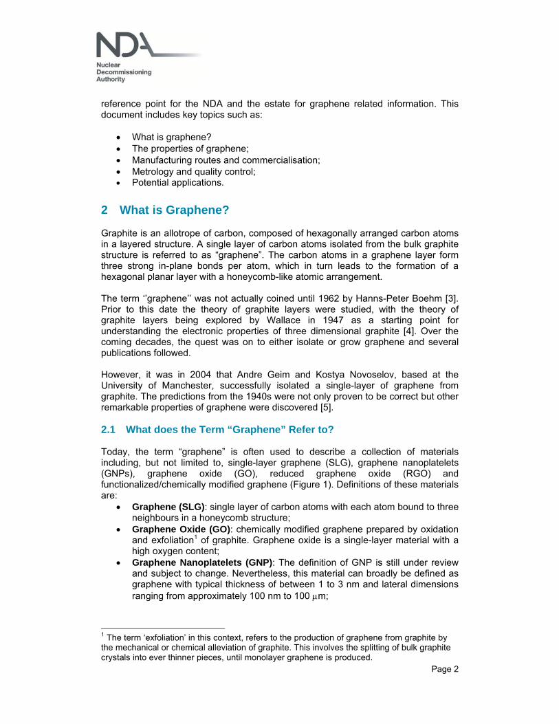
However, it was in 2004 that Andre Geim and Kostya Novoselov, based at the University of Manchester, successfully isolated a single-layer of graphene from graphite. The predictions from the 1940s were not only proven to be correct but other remarkable properties of graphene were discovered [5]. 2.1 What does the Term “Graphene” Refer to? Today, the term “graphene” is often used to describe a collection of materials including, but not limited to, single-layer graphene (SLG), graphene nanoplatelets (GNPs), graphene oxide (GO), reduced graphene oxide (RGO) and functionalized/chemically modified graphene (Figure 1). Definitions of these materials are:
Graphene (SLG): single layer of carbon atoms with each atom bound to three neighbours in a honeycomb structure;
Graphene Oxide (GO): chemically modified graphene prepared by oxidation and exfoliation1 of graphite. Graphene oxide is a single-layer material with a high oxygen content;
Graphene Nanoplatelets (GNP): The definition of GNP is still under review and subject to change. Nevertheless, this material can broadly be defined as graphene with typical thickness of between 1 to 3 nm and lateral dimensions ranging from approximately 100 nm to 100 m;
1 The term ‘exfoliation’ in this context, refers to the production of graphene from graphite by the mechanical or chemical alleviation of graphite. This involves the splitting of bulk graphite crystals into ever thinner pieces, until monolayer graphene is produced.
Page 3
Reduced Graphene Oxide (RGO): A material (often of monolayer form) obtained by the chemical or thermal reduction of GO.
Figure 1: Common Types of Graphene Materials
All of the above can be viewed as different types of two-dimensional crystals. The electronic structure and properties of graphene rapidly evolve with the number of layers, approaching the 3D limit of graphite, at approximately 10 layers. As previously described, graphene can be present in many forms. In the most pristine form graphene is, at least for the most part, isolated, not having any mechanical support from other compounds or structures. This isolated graphene is realised in suspended membranes or beams often measuring tens of microns laterally, yet only one or a few atoms thick.
Page 4
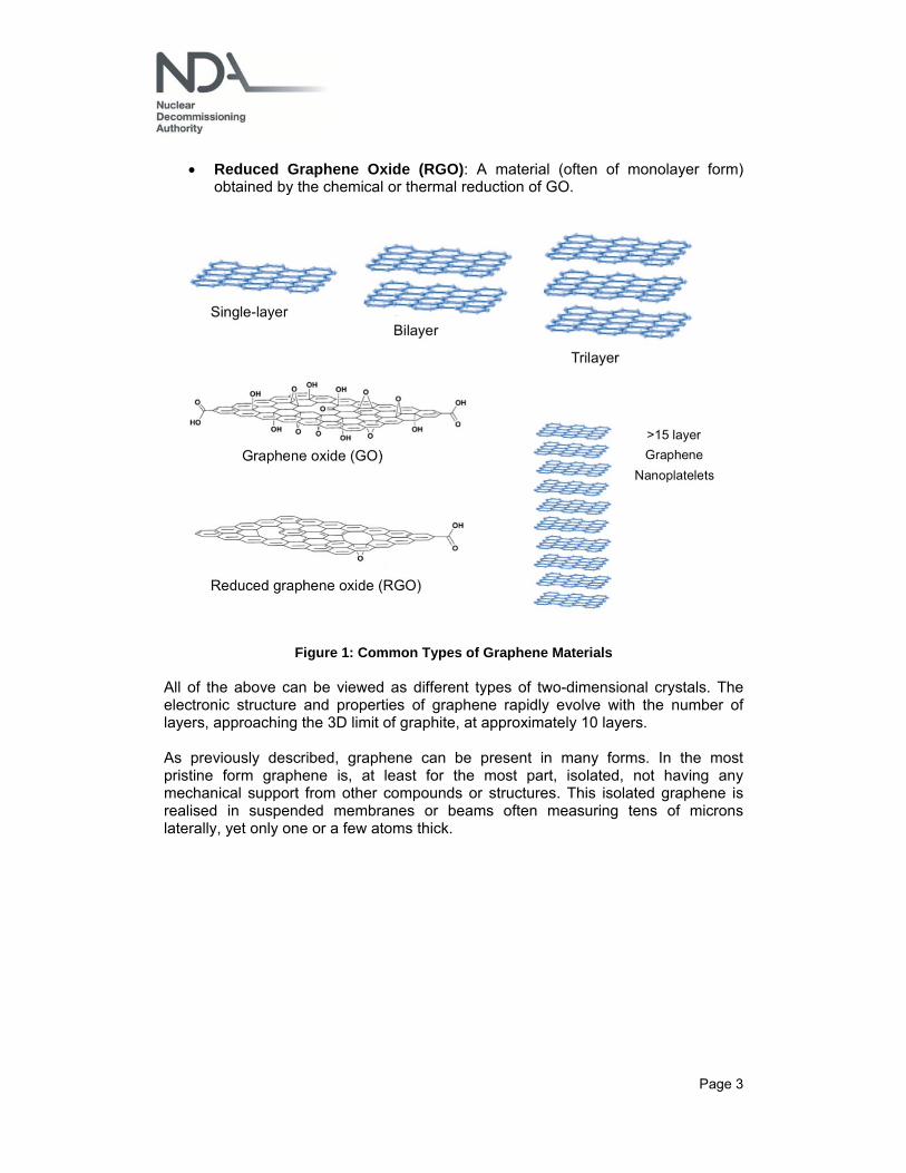
Most frequently, however graphene is directly fabricated or transferred onto a substrate to form macroscopic materials, such as that shown in Figure 2, which shows a microscopy image of graphene transferred onto a grid. The direct fabrication of graphene onto substrates is described further in Section 4. The interaction between the graphene and the substrate can result in the modification of the intrinsic properties of the material. The most graphene-friendly substrate known today is boron-nitride (BN). Once transferred onto BN graphene retains most of its intrinsic properties. Furthermore, BN is also a good encapsulation material, isolating graphene from the unwanted effects of environment.
Figure 2: Scanning Electron Microscopy Image of a Graphene Membrane Transferred
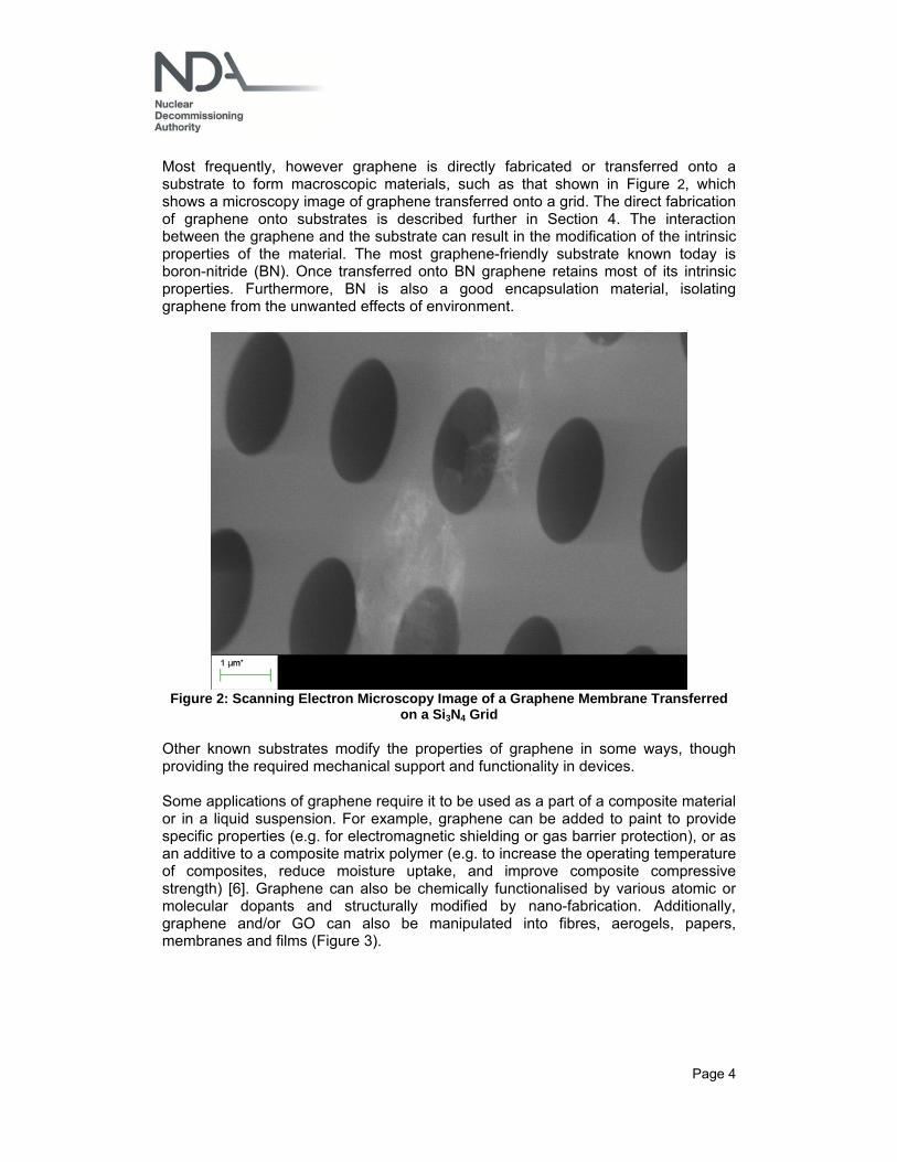
on a Si3N4 Grid Other known substrates modify the properties of graphene in some ways, though providing the required mechanical support and functionality in devices. Some applications of graphene require it to be used as a part of a composite material or in a liquid suspension. For example, graphene can be added to paint to provide specific properties (e.g. for electromagnetic shielding or gas barrier protection), or as an additive to a composite matrix polymer (e.g. to increase the operating temperature of composites, reduce moisture uptake, and improve composite compressive strength) [6]. Graphene can also be chemically functionalised by various atomic or molecular dopants and structurally modified by nano-fabrication. Additionally, graphene and/or GO can also be manipulated into fibres, aerogels, papers, membranes and films (Figure 3).
Page 5
Figure 3: Graphene and its Derived Forms
3 The Properties of Graphene The unique properties of graphene and its derivatives are the major areas of interest, each of which seems to be superior to rival materials. This material boasts a plethora of unique properties that include:
The world’s strongest material: the specific strength of graphene is 48 000 kN m kg−1, which is over 300 times higher than the specific strength of steel (steel specific strength = 154 kN m kg−1), yet being extremely lightweight;
High thermal conductivity: the conductivity of graphene is approximately 3000 W mK-1, compared to ~400 W mK-1 for copper;
High electrical conductivity: the ability to sustain extremely high densities of electric current (a million times higher than copper);
Very elastic; Readily chemically functionalised: making the material very versatile and
allowing graphene to be incorporated into a range of devices and materials to suit the intended application;
Impermeable: to any atomic or molecular species, with the exception of hydrogen ions which will be discussed further in Section 6.1.
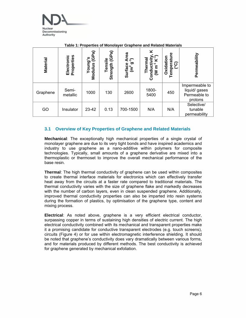
Some physical properties of graphene and GO are summarised in Table 1 [7, 8, 9], while further details relating to graphene related materials are provided below.
Page 6
Table 1: Properties of Monolayer Graphene and Related Materials M
ater
ial
Ele
ctro
nic
P
rop
erti
es
Yo
un
g’s
M
od
ulu
s (G
Pa)
Ten
sile
S
tren
gth
(G
Pa)
Su
rfac
e A
rea
(m2 g
-1)
Th
erm
al
Co
nd
uct
ivit
y, K
(W
m-1
K-1
)
Oxi
dat
ion
T
emp
erat
ure
(°
C)
Per
mea
bili
ty
Graphene Semi-
metallic 1000 130 2600
1800-5400
450
Impermeable to liquid/ gases Permeable to
protons
GO Insulator 23-42 0.13 700-1500 N/A N/A Selective/ tunable
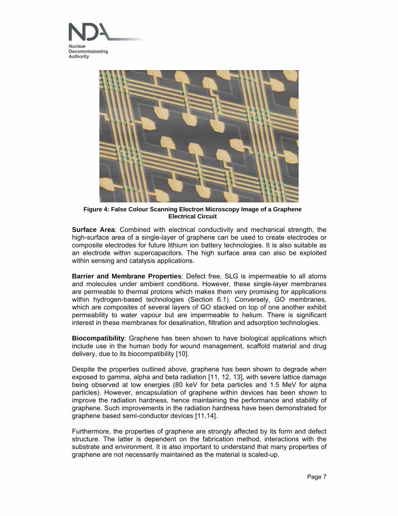
permeability 3.1 Overview of Key Properties of Graphene and Related Materials Mechanical: The exceptionally high mechanical properties of a single crystal of monolayer graphene are due to its very tight bonds and have inspired academics and industry to use graphene as a nano-additive within polymers for composite technologies. Typically, small amounts of a graphene derivative are mixed into a thermoplastic or thermoset to improve the overall mechanical performance of the base resin. Thermal: The high thermal conductivity of graphene can be used within composites to create thermal interface materials for electronics which can effectively transfer heat away from the circuits at a faster rate compared to traditional materials. The thermal conductivity varies with the size of graphene flake and markedly decreases with the number of carbon layers, even in clean suspended graphene. Additionally, improved thermal conductivity properties can also be imparted into resin systems during the formation of plastics, by optimisation of the graphene type, content and mixing process. Electrical: As noted above, graphene is a very efficient electrical conductor, surpassing copper in terms of sustaining high densities of electric current. The high electrical conductivity combined with its mechanical and transparent properties make it a promising candidate for conductive transparent electrodes (e.g. touch screens), circuits (Figure 4) or for use within electromagnetic interference shielding. It should be noted that graphene’s conductivity does vary dramatically between various forms, and for materials produced by different methods. The best conductivity is achieved for graphene generated by mechanical exfoliation.
Page 7
Surface Area: Combined with electrical conductivity and mechanical strength, the high-surface area of a single-layer of graphene can be used to create electrodes or composite electrodes for future lithium ion battery technologies. It is also suitable as an electrode within supercapacitors. The high surface area can also be exploited within sensing and catalysis applications. Barrier and Membrane Properties: Defect free, SLG is impermeable to all atoms and molecules under ambient conditions. However, these single-layer membranes are permeable to thermal protons which makes them very promising for applications within hydrogen-based technologies (Section 6.1). Conversely, GO membranes, which are composites of several layers of GO stacked on top of one another exhibit permeability to water vapour but are impermeable to helium. There is significant interest in these membranes for desalination, filtration and adsorption technologies. Biocompatibility: Graphene has been shown to have biological applications which include use in the human body for wound management, scaffold material and drug delivery, due to its biocompatibility [10]. Despite the properties outlined above, graphene has been shown to degrade when exposed to gamma, alpha and beta radiation [11, 12, 13], with severe lattice damage being observed at low energies (80 keV for beta particles and 1.5 MeV for alpha particles). However, encapsulation of graphene within devices has been shown to improve the radiation hardness, hence maintaining the performance and stability of graphene. Such improvements in the radiation hardness have been demonstrated for graphene based semi-conductor devices [11,14]. Furthermore, the properties of graphene are strongly affected by its form and defect structure. The latter is dependent on the fabrication method, interactions with the substrate and environment. It is also important to understand that many properties of graphene are not necessarily maintained as the material is scaled-up.
Figure 4: False Colour Scanning Electron Microscopy Image of a Graphene Electrical Circuit
Page 8
4 Manufacturing Routes and Commercialisation In 2004 A. Geim, K. Novoselov and colleagues at the University of Manchester demonstrated an ingenious way to isolate and detect graphene and the graphene story began. Graphene was obtained by micro-mechanical alleviation (“exfoliation”) of graphite. Researchers used adhesive tape to exfoliate, or alleviate graphite layers from the bulk material and repeatedly split graphite crystals into increasingly thinner pieces. Relatively large crystals (first, only a few micrometres in size but, eventually, larger than 1 mm and visible by the naked eye) were obtained by the technique, which is often referred to as the “scotch tape method”. The method is still used to produce highest quality graphene samples for research purposes. Needless to say that graphene production by the scotch-tape method is not scalable and as a result multiple methods for graphene manufacture have since been devised. More advanced methods to manufacture graphene can be broadly split into two groups – ‘top down’ and ‘bottom up’ methods. The top down approach includes the exfoliation method described previously and essentially involves starting with bulk material, such as graphite, and repeatedly removing graphite layers to create ever thinner layers. The bottom up approach involves depositing carbon onto a mechanical support or substrate to create graphene layers. Typically, single or bilayer graphene is obtained from the micromechanical exfoliation method (top down) or from Chemical Vapour Deposition (CVD) techniques (bottom up). GNPs, GO and RGO are usually produced from Liquid Phase Exfoliation (LPE) methods, which is a top down approach, and come in the form of either dispersions or dry powders. A description of the common manufacturing routes, including the advantages, disadvantages and applications are presented in Table 2. Other methods of graphene production, such as molecular-beam epitaxy and laser ablation have been developed [6, 15]. Molecular-beam epitaxy involves depositing gaseous graphite onto a support/ substrate under high vacuum, while laser ablation utilises a pulsed laser beam to generate graphene structures from bulk graphite. These methods are intended for certain niche applications so have not been included in this report.
Page 9
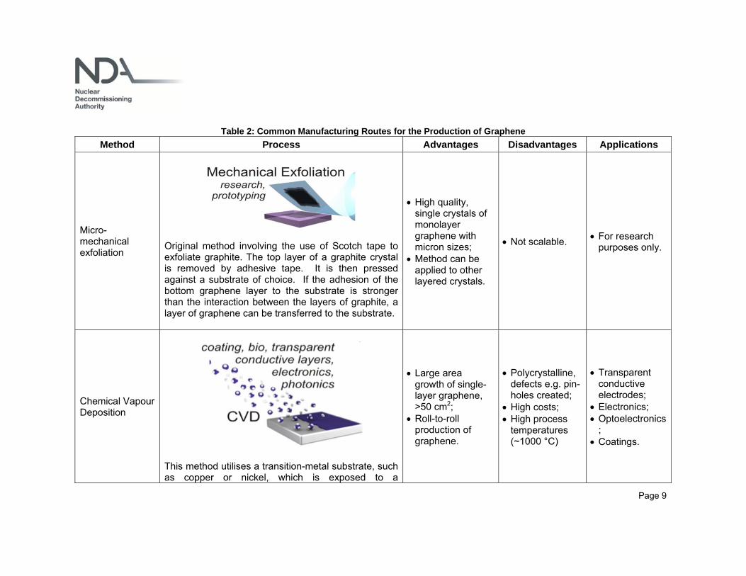
Table 2: Common Manufacturing Routes for the Production of Graphene
Method Process Advantages Disadvantages Applications
Micro-mechanical exfoliation
Original method involving the use of Scotch tape to exfoliate graphite. The top layer of a graphite crystal is removed by adhesive tape. It is then pressed against a substrate of choice. If the adhesion of the bottom graphene layer to the substrate is stronger than the interaction between the layers of graphite, a layer of graphene can be transferred to the substrate.
High quality, single crystals of monolayer graphene with micron sizes;
Method can be applied to other layered crystals.
Not scalable. For research
purposes only.
Chemical Vapour Deposition
This method utilises a transition-metal substrate, such as copper or nickel, which is exposed to a
Large area growth of single-layer graphene, >50 cm2;
Roll-to-roll production of graphene.
Polycrystalline, defects e.g. pin-holes created;
High costs; High process
temperatures (~1000 °C)
Transparent conductive electrodes;
Electronics; Optoelectronics
; Coatings.
Page 10
Method Process Advantages Disadvantages Applications
hydrocarbon gas (often methane) at high temperature. Graphene growth proceeds on the substrate surface via thermal decomposition of hydrocarbons on the surface, or by surface segregation of carbon upon cooling from a metastable carbon-metal solid solution. Graphene growth can be self-terminated after a single layer by very low gas pressure, and in particular, on a copper substrate. However, bi-layer and multi-layer graphene can also be obtained on different metals and using heavier hydrocarbons.
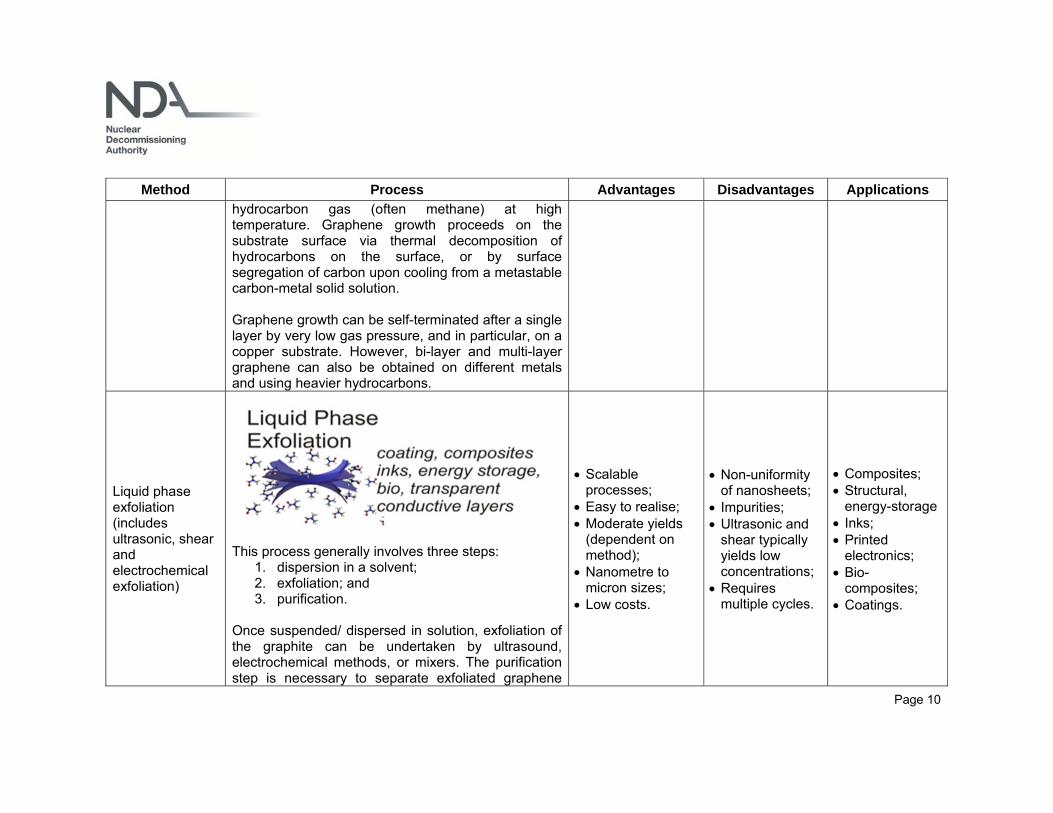
Liquid phase exfoliation (includes ultrasonic, shear and electrochemical exfoliation)
This process generally involves three steps:
1. dispersion in a solvent; 2. exfoliation; and 3. purification.
Once suspended/ dispersed in solution, exfoliation of the graphite can be undertaken by ultrasound, electrochemical methods, or mixers. The purification step is necessary to separate exfoliated graphene
Scalable processes;
Easy to realise; Moderate yields
(dependent on method);
Nanometre to micron sizes;
Low costs.
Non-uniformity of nanosheets;
Impurities; Ultrasonic and
shear typically yields low concentrations;
Requires multiple cycles.
Composites; Structural,
energy-storage Inks; Printed
electronics; Bio-
composites; Coatings.
Page 11
Method Process Advantages Disadvantages Applications
from un-exfoliated flakes, and usually requires ultracentrifugation.
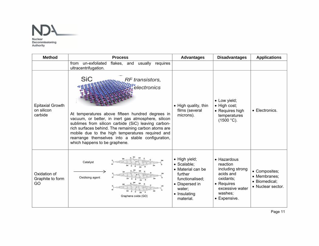
Epitaxial Growth on silicon carbide
At temperatures above fifteen hundred degrees in vacuum, or better, in inert gas atmosphere, silicon sublimes from silicon carbide (SiC) leaving carbon-rich surfaces behind. The remaining carbon atoms are mobile due to the high temperatures required and rearrange themselves into a stable configuration, which happens to be graphene.
High quality, thin films (several microns).
Low yield; High cost; Requires high
temperatures (1500 °C).
Electronics.
Oxidation of Graphite to form GO
High yield; Scalable; Material can be
further functionalised;
Dispersed in water;
Insulating material.
Hazardous reaction including strong acids and oxidants;
Method Process Advantages Disadvantages Applications
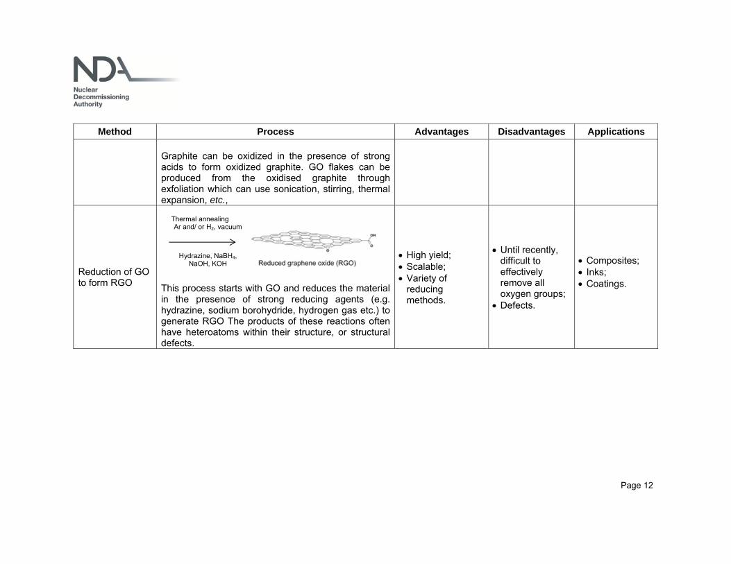
Graphite can be oxidized in the presence of strong acids to form oxidized graphite. GO flakes can be produced from the oxidised graphite through exfoliation which can use sonication, stirring, thermal expansion, etc.,
Reduction of GO to form RGO
This process starts with GO and reduces the material in the presence of strong reducing agents (e.g. hydrazine, sodium borohydride, hydrogen gas etc.) to generate RGO The products of these reactions often have heteroatoms within their structure, or structural defects.
High yield; Scalable; Variety of
reducing methods.
Until recently, difficult to effectively remove all oxygen groups;
Defects.
Composites; Inks; Coatings.
Thermal annealing Ar and/ or H2, vacuum
Hydrazine, NaBH4, NaOH, KOH
Page 13
5 Graphene Metrology The upscaling of graphene (and related materials) production is steadily progressing, but challenges remain when it comes to maintaining the quality, properties and performance in mass production. The desirable properties of graphene itself cannot be given in absolute terms, as it depends on the applications. For example, the desirable properties of graphene needed for high performance electronics include being defect free and flat, which is the opposite of that required for batteries or supercapacitors, where the material functions better with materials having defects, voids and cavities. Therefore, the development of reliable methods for graphene metrology, quality control and standardisation is extremely important. Due to graphene being only one atom thick, its detection and identification initially appeared to be seemingly complicated and potentially not possible. However, upon research into graphene metrology methods, it was found that despite the unusual properties displayed by the material, graphene metrology was straightforward and readily implemented. Although atomically thin, graphene absorbs a measurable fraction of white light. When graphene is stretched across a slit the absorption can be accurately measured and the number of layers in a particular sample can be counted. A much more practical method of graphene identification makes use of the optical interference present in the thermally oxidised surface of silicon – a common substrate for exfoliated graphene. Graphene monolayers and multilayers give different contrast under illumination allowing for the straightforward determination of the number of graphene layers. This method however does not work for all graphene related materials, particularly graphene on SiC. However, Low Energy Electron Microscopy and Low Energy Electron Diffraction and scattering (LEEM and LEED), can be used for this form of graphene, which are similar variants of ‘normal’ electron microscopy and diffraction techniques. Another technique that has proved to be very helpful in graphene studies is Raman spectroscopy and allows evaluation of structural disorder, doping etc. Raman spectroscopy can be performed on a local level allowing distribution of the physical parameters to be measured. Other techniques employed include:
High Resolution Transmission Electron Microscopy (HRTEM); Photoemission methods, such as Angular Resolved Photoemission
Spectroscopy (ARPES); Scanning probe microscopy, such as the Scanning Kelvin Probe Microscopy,
(SKPM). In recent years the emphasis has shifted to the development of rapid, non-invasive methods of graphene quality control, which could be used on graphene production lines. In particular, optical, microwave and terahertz methods and instrumentation have been developed to measure the defect, void and cavity properties of graphene in a controlled environment.
Page 14
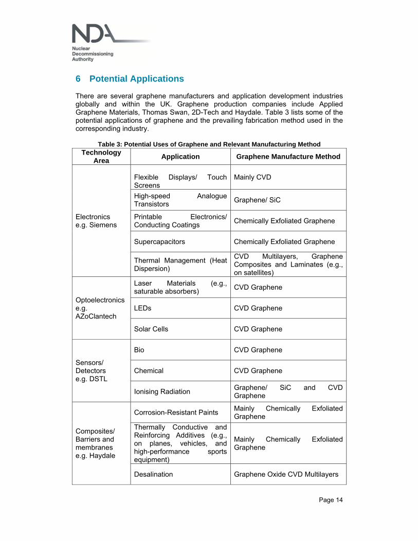
6 Potential Applications There are several graphene manufacturers and application development industries globally and within the UK. Graphene production companies include Applied Graphene Materials, Thomas Swan, 2D-Tech and Haydale. Table 3 lists some of the potential applications of graphene and the prevailing fabrication method used in the corresponding industry.
Table 3: Potential Uses of Graphene and Relevant Manufacturing Method Technology
Area Application Graphene Manufacture Method
Electronics e.g. Siemens
Flexible Displays/ Touch Screens
Mainly CVD
High-speed Analogue Transistors
Graphene/ SiC
Printable Electronics/ Conducting Coatings
Chemically Exfoliated Graphene
Supercapacitors Chemically Exfoliated Graphene
Thermal Management (Heat Dispersion)
CVD Multilayers, Graphene Composites and Laminates (e.g., on satellites)
Thermally Conductive and Reinforcing Additives (e.g., on planes, vehicles, and high-performance sports equipment)
Mainly Chemically Exfoliated Graphene
Desalination Graphene Oxide CVD Multilayers
Page 15
Technology Area
Application Graphene Manufacture Method
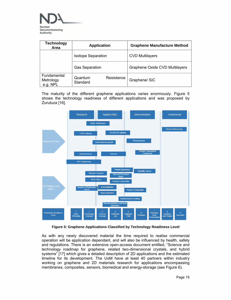
Isotope Separation CVD Multilayers
Gas Separation Graphene Oxide CVD Multilayers
Fundamental Metrology e.g. NPL
Quantum Resistance Standard
Graphene/ SiC
The maturity of the different graphene applications varies enormously. Figure 5 shows the technology readiness of different applications and was proposed by Zurutuza [16].
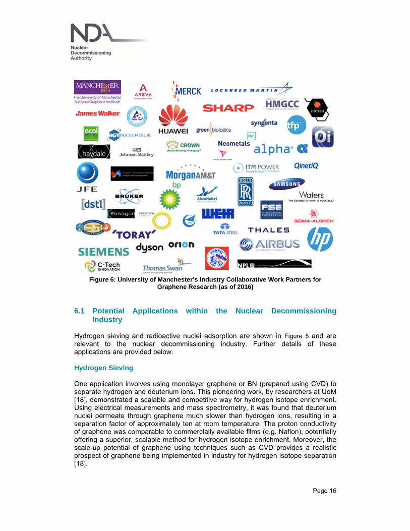
Figure 5: Graphene Applications Classified by Technology Readiness Level As with any newly discovered material the time required to realise commercial operation will be application dependant, and will also be influenced by health, safety and regulations. There is an extensive open-access document entitled, “Science and technology roadmap for graphene, related two-dimensional crystals, and hybrid systems” [17] which gives a detailed description of 2D applications and the estimated timeline for its development. The UoM have at least 40 partners within industry working on graphene and 2D materials research for applications encompassing membranes, composites, sensors, biomedical and energy-storage (see Figure 6).
Page 16
Figure 6: University of Manchester’s Industry Collaborative Work Partners for
Graphene Research (as of 2016) 6.1 Potential Applications within the Nuclear Decommissioning
Industry Hydrogen sieving and radioactive nuclei adsorption are shown in Figure 5 and are relevant to the nuclear decommissioning industry. Further details of these applications are provided below. Hydrogen Sieving One application involves using monolayer graphene or BN (prepared using CVD) to separate hydrogen and deuterium ions. This pioneering work, by researchers at UoM [18], demonstrated a scalable and competitive way for hydrogen isotope enrichment. Using electrical measurements and mass spectrometry, it was found that deuterium nuclei permeate through graphene much slower than hydrogen ions, resulting in a separation factor of approximately ten at room temperature. The proton conductivity of graphene was comparable to commercially available films (e.g. Nafion), potentially offering a superior, scalable method for hydrogen isotope enrichment. Moreover, the scale-up potential of graphene using techniques such as CVD provides a realistic prospect of graphene being implemented in industry for hydrogen isotope separation [18].
Page 17
The ability of graphene to act as a hydrogen sieve could potentially enable it to function in the remediation of radioactive hydrogen species such as deuterium and tritium, from non-radioactive hydrogen. Radionuclide Removal The use of GO has been demonstrated for the rapid removal of some of the most toxic and radioactive long-lived human-made radionuclides from contaminated water, even present in acidic solutions. Although detection of radionuclide contamination is relatively simple, their removal from contaminated aqueous media is still a challenging and costly procedure. The key issue is a lack of specific and low-cost sorbent material for radionuclide removal. Although there are several sorbents effective under laboratory conditions, their effectiveness quickly diminishes in natural waters, where natural ions sorption competes with radionuclides. A study investigated the interaction of GO with actinides including Am(III), Th(IV), Pu(IV), Np(V), U(VI) and typical fission products Sr(II), Eu(III) and Tc(VII), along with their sorption kinetics [19]. GO demonstrated high sorption affinity towards the most toxic radionuclides from various solutions. The removal of radionuclides from solutions was tested using a simulated liquid waste that contained uranium, plutonium, sodium and calcium ions in addition to common complexing agents, such as carbonate, sulfate, acetate and citrate. GO demonstrated very high sorption ability towards the actinide ions (80% sorption for plutonium) when compared to bentonite and activated carbon, despite the fact that actinides form strong complexes with citrate and acetate. Coagulation of the GO occurred upon sorption of radionuclides, forming nanoparticle aggregates of GO sheets. Therefore, GO-containing radionuclide could also be easily coagulated, precipitated and hence removed. These advantages combined with the potential of industrial scale-up for GO, makes it a promising new material for radionuclide containment and removal [19]. In addition to the sorption properties of GO, the efficacy of graphene enhanced composite materials has also been demonstrated for the removal of uranium from aqueous solutions. One such example utilised GO/amidoxime hydrogel (AGH) [20] for the removal of uranium species from various solutions, including seawater. Even in the presence of high concentrations of competing ions (e.g. Mg2+, Ca2+, Ba2+ and Sr2+), AGH displayed an enhanced selectivity for uranium. Ionising Radiation Detection A number of groups, including Canberra Industries, Purdue University (IN, USA) and Penn State University (PA, USA) have demonstrated graphene based Field Effect Transistors (FETs) for detection of X-rays, gamma-rays, neutrons and alpha particles [21, 22]. Graphene-based detectors represent attractive technologies that could meet the need for inexpensive, low-power, size-scalable detection architectures, which are sensitive to X-rays, gamma-rays, and neutrons. These devices work on the principle that ionising radiation interacts with graphene, depositing energy and changing the materials electric field. This radiation induced event is then measured (e.g. through changes in the resistance, or current of graphene).
Page 18
7 Conclusion Graphene is a novel material, being the first one atom thick, 2D material that has been isolated. Its honeycomb-like, planar hexagonal carbon atom arrangement and 2D nature, gives graphene and its related compounds, some novel properties. These properties include: high mechanical strength (whilst being lightweight), high thermal and electrical conductivity, extremely large surface area and barrier/ membrane properties. These properties have made graphene an exciting proposition in the research world. Since first being isolated from graphite, in 2004, utilising a micro-mechanical alleviation (“exfoliation”) or the “scotch-tape method”, many other methods have been developed to manufacture graphite including, micro-mechanical exfoliation, CVD and LPE. The majority of these developed methods are scalable, allowing for mass manufacture of graphene for use in practical applications. It has however been identified that the ‘quality’ of graphene (subjective term, dependant on the graphene application) produced and therefore the properties and performance of the graphene, does vary depending on the method of manufacture. This has hence led to the development of reliable methods for graphene metrology, quality control and standardisation. The intrinsic properties of graphene has resulted in graphene having many potential practical applications in the areas of, electronics, optoelectronics, sensors/ detectors, composites/ barriers and fundamental metrology. Each of these applications is at varying stages of technology readiness. In relation to the nuclear decommissioning industry, potential applications have already been identified, utilising graphene’s membrane like quality to function as a hydrogen isotope ‘sieve’, the affinity of GO for metallic ions and the use of graphene in ionising radiation detectors. Due to the variety of intrinsic properties of graphene, it is hypothesised that graphene could have other future applications within the nuclear decommissioning industry. A report documenting the identified synergies between the NDA estate decommissioning R&D needs and graphene research will be produced upon the conclusion of this project. The report will also identify potential current research gaps that could be investigated to further increase the opportunity for the use of graphene in the nuclear decommissioning industry.
8 Further Information For further information regarding graphene, its properties and current research areas please see Table 4.
Page 19
Table 4: Sources for Further Graphene-Related Information Research Groups/
Organisations Journals Conferences
Graphene Special Interest Group (SIG);
National Graphene Institute (NGI), University of Manchester;
National Graphene Metrology Centre (NGMC), National Physical Laboratory;
Cambridge Graphene Centre (CGC), Cambridge University;
Innovate UK, UK Innovation Agency sponsored by the Department for Business, Energy and Industrial Strategy;
GrapheneTechnology - The Official Journal of The Graphene Council, ISSN: 2365-631X (electronic version);
FlatChem, Chemistry of Flat Materials, ISSN Online: 2452-2627;
Graphene and 2D Materials, Emerging Science, ISSN Online: 2299-3134
2016 Graphene & 2-D Materials Conference: From Research to Applications - 16-17th November 2016, London, UK
48th Annual Meeting on Nuclear Technology (AMNT 2017) - 16-17th May 2017, Berlin, Germany;
Graphene Week 2017 - 25-29th September 2017, Athens, Greece.
Page 20
9 References 1 NDA, Research and Development – 5 Year Research and Development Plan,
Issue 1, December 2013
2 Clarivate Analytics, Web of Science™ – The world’s most trusted citation index covering the leading scholarly literature
3 Graphene Think Piece, Knowledge Transfer Network: Chemistry Innovation, October 2013
4 P R Wallace, The Band Theory of Graphite, Phys. Rev. 71, 622, 1947
5 D R Dreyer, R S Ruoff and C W Bielawski, From Conception to Realisation: an Historical Account of Graphene and some Perspectives for its Future, Angew. Chem. Int. Ed., 49, 9336-9344, 2010 [OPEN ACCESS]
6 K S Novoselov, V I Fal’ko and L Colombo, A Roadmap for Graphene, Nature, 490, 192-200, 2012
7 S Chuah and Z Pan et. al., Nano Reinforced Cement and Concrete Composites and New Perspective from Graphene Oxide, Construction and Building Materials, 73, 113–124, 2014 [OPEN ACCESS]
8 S Bertolazzi, J Brivio and A Kis, Stretching and Breaking of Ultrathin MoS2, ACS Nano, 5, 12, 9703-9709, (2011)
9 R Yan and J R Simpson et. al., Thermal Conductivity of Monolayer Molybdenum Disulfide Obtained from Temperature-Dependent Raman Spectroscopy, ACS Nano, 8, 1, 986-993, (2014)
10 A M Pinto et. al., Graphene-Based Materials Biocompatibility: A Review, Colloids and Surfaces B: Biointerfaces, 111, 188-202, 2013
11 K Alexandrou, A Masurkar and H Edress et. al., Improving the Radiation Hardness of Graphene Field Effect Transistors, Appl. Physics Letters, 109, 2016 [OPEN ACCESS]
12 A Ansón-Casaos, J A Puértolas, F J Pascual et. al., The Effect of Gamma-Irradiation on Few-Layered Graphene Materials, Appl. Surface Sci., 301, 264-272, 2014 [OPEN ACCESS]
13 Y Wang, Y Feng, F Mo et. al., Influence of irradiation upon few-layered graphene using electron-beams and gamma-rays, Appl. Physics Letters, 102, 2014
14 K Alexandrou, Ionizing Radiation Effects on Graphene Based Field Effects Transistors, Doctor of Philosophy Thesis, Columbia University, 2016 [OPEN ACCESS]
Page 21
15 S Dhar, A Roy Barman and G X Ni et al., A New Route to Graphene Layers
16 W Ren and H-M Cheng, The Global Growth of Graphene, Nature Nanotechnology 9, 730–734, 2014 [OPEN ACCESS]
17 Science and technology roadmap for graphene, related two-dimensional crystals, and hybrid systems, Nanoscale, 7, 4598 (2015) [OPEN ACCESS]
18 M Lozada-Hidalgo and S. Hu et. al., Sieving Hydrogen Isotopes Through two Dimensional Crystals, Science, 351, 68-70, 2016
19 A Y Romanchuk et. al, Graphene Oxide for Effective Radionuclide Removal, Phys. Chem. Chem. Phys., 15, 2321-2327, (2013)
20 F Wang, H Li and Q Liu, et.al., A Graphene Oxide/Amidoxime Hydrogel for Enhanced Uranium Capture, Scientific Reports (DOI: 10.1038/srep19367), 2016 [OPEN ACCESS]
21 A Patil et. al, Graphene Field Effect Transistors for Detection of Ionizing Radiation, IEEE Nuclear Science Symposium Conference Record (NSS/MIC), 2010 [OPEN ACCESS]
22 O Koybasi, E Cazalas, I Childres et. al., Detection of light, X-rays, and gamma rays using graphene field effect transistors fabricated on SiC, CdTe, and AlGaAs/GaAs substrates, 2013 IEEE Nuclear Science Symposium and Medical Imaging