MAHARASHTRASTATE BOARD OF TECHNICAL EDUCATION (Autonomous)
(ISO/IEC - 27001 - 2005 Certified)
Page1
MODEL ANSWER SUMMER– 17 EXAMINATION
Subject Title: Elements of Electronics Subject Code: Important Instructions to examiners:
1) The answers should be examined by key words and not as word-to-word as given in the model answer scheme.
2) The model answer and the answer written by candidate may vary but the examiner may try to assess the understanding level of the candidate.
3) The language errors such as grammatical, spelling errors should not be given more Importance (Not applicable for subject English and Communication Skills.
4) While assessing figures, examiner may give credit for principal components indicated in the figure. The figures drawn by candidate and model answer may vary. The examiner may give credit for anyequivalent figure drawn.
5) Credits may be given step wise for numerical problems. In some cases, the assumed constant values may vary and there may be some difference in the candidate’s answers and model answer.
6) In case of some questions credit may be given by judgement on part of examiner of relevant answer based on candidate’s understanding.
7) For programming language papers, credit may be given to any other program based on equivalent concept.
Q.
No.
Sub
Q.N.
Answer Marking
Scheme
Q.1 Attempt any TEN: 20-Total
Marks
(a) What is magnetic material ? State it’s two applications. 2M
Ans: Magnetic materials are those materials that can be either attracted or repelled when
placed in an external magnetic field and can be magnetized themselves.
OR
The materials which provide path to the magnetic flux and can be magnetized are called
magnetic materials.
Applications: 1.Floppy disc ,hard disc
2.Motors and generators
3.Biomedical equipment
1M
1M
(b) Define Inductor. Draw its symbol. 2M
Ans: An inductor is a passive electronic component that stores energy in the form of a
magnetic field
1M
1M
17215XXXXX
MAHARASHTRASTATE BOARD OF TECHNICAL EDUCATION (Autonomous)
(ISO/IEC - 27001 - 2005 Certified)
Page2
(c) What is dielectric material? Enlist dielectric material used in capacitor. 2M
Ans: A dielectric material is an electrical insulator that can be polarized by an applied electric
field.
Dielectric materials used in capacitor: porcelain (ceramic), mica, glass, plastics, and
the oxides of various metals
1M
1M
(d) State any Four applications of PN junction diode. 2M
Ans: 1. Rectifiers in power supplies,
2. Detectors in RF,
3 .Clippers,
4. In clamping networks used as DC Restorers,
5. As switches in digital logic circuits.
(½ M for
each point)
(e) Draw symbol of (i) Tunnel diode (ii) LED 2M
Ans:
(i) Tunnel diode:
(ii) LED:
1M
1M
(f) Calculate equivalent resistance IFRI and R2 resistors are conncted in parallel R1 =
10 Ω, R2 = 5 Ω
2M
Ans:
1M for
Formula
1M for
Answer
(g) Define (i) Open circuit (ii) Short circuit. 2M
Ans: Open circuit : An electrical circuit is said to be open,when any part of conducting path is
open or broken and there is no continuity in the conducting path of an electrical circuit.
1M
MAHARASHTRASTATE BOARD OF TECHNICAL EDUCATION (Autonomous)
(ISO/IEC - 27001 - 2005 Certified)
Page3
Short circuit : An electrical circuit is said to be short,when voltage source has closed
path across its terminal.( or any relevent definition) 1M
(h) State Kirchhoff’s voltage law. 2M
Ans: The algebraic sum of all the emf’s in a loop is equal to zero. 2M
Correct
Statement
(i) State the need of Rectifier circuits. 2M
Ans: The DC power supply is essential for operation of many electronic devices and
circuits.This DC voltage is obtained from AC source.Rectifier circuit is important circuit
for this conversion.
2M
Correct
Statement
(j) State types of filters. 2M
Ans: 1. Shunt capacitor filter
2. Series inductor filter (Choke filter)
3. Choke input filter ( LC or L type filter )
4. Capacitor input filter ( CLC or )
½ M
for each
point
(k) What is need of wave shaping circuit ? 2M
Ans: In electronics application, it is often needed to alter the shape of wveform like cutting off
positive or negative portion of wave,generation of one wave from other,holding wave at
some dc level etc.To do this waveshaping circuits are needed.
Correct
statement
2M
(l) Draw RC differentiator circuit. 2M
Ans:
2M
Q 2 Attempt any FOUR : 16M
(a) Write down the colour code for following resistor :
(i) 150 Ω ± 5% (ii) 4’6kΩ ±20%
4M
Ans: (i) Brown, Green, Brown, Gold
(ii) Yellow,blue,red,no colour
2M
2M
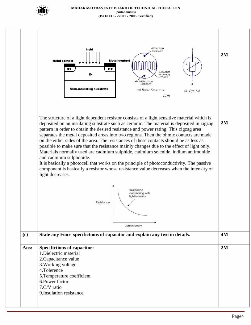
(b) With help of constructional diagram, explain working of LDR. 4M
Ans:
MAHARASHTRASTATE BOARD OF TECHNICAL EDUCATION (Autonomous)
(ISO/IEC - 27001 - 2005 Certified)
Page4
The structure of a light dependent resistor consists of a light sensitive material which is
deposited on an insulating substrate such as ceramic. The material is deposited in zigzag
pattern in order to obtain the desired resistance and power rating. This zigzag area
separates the metal deposited areas into two regions. Then the ohmic contacts are made
on the either sides of the area. The resistances of these contacts should be as less as
possible to make sure that the resistance mainly changes due to the effect of light only.
Materials normally used are cadmium sulphide, cadmium selenide, indium antimonide
and cadmium sulphonide.
It is basically a photocell that works on the principle of photoconductivity. The passive
component is basically a resistor whose resistance value decreases when the intensity of
light decreases.
2M
2M
(c) State any Four specifictions of capacitor and explain any two in details. 4M
Ans: Specifictions of capacitor: 1.Dielectric material
2.Capacitance value
3.Working voltage
4.Tolerence
5.Temperature coefficient
6.Power factor
7.C/V ratio
9.Insulation resistance
2M
MAHARASHTRASTATE BOARD OF TECHNICAL EDUCATION (Autonomous)
(ISO/IEC - 27001 - 2005 Certified)
Page5
Explanation:
1.Working voltage : It is the maximum voltage at which capacitor can operate without
failure
2.Power factor : It is the ratio of resistance to reactance at the operating frequency.
3 Tolerance: It is the maximum possible deviation on either side from actual value.
4.C/V ratio: It is the ratio of capacitance to volume.
Note:-(Students can explain other specification)
2M
(d) With help of constructiobal diagram, explain working of slug tunned inductor. 4M
Ans:
The variable inductor having an adjustable ferrite core is known as slug tuned inductor.
The value of inductance increases or decreases respectively, due to the movement of a
ferrite core into or out of the coil winding. The basic construction of a slug tuned
inductor is shown in fig.This construction is similar to the fixed ferrite core inductor but
the core is adjustable.The value of inductance increases, when the slug is moved into the
coil windingand decreases the resonant frequency of the tuned circuit. When the slug is
moved out of the coil winding, the inductance decrease and the resonant frequency of the
tuned circuit increases.The value of inductance can be varied by using movable core
which can be moved up or down by using screw driver.
2M
2M
(e) Draw and explain V-I characteristics of a P-N junction diode. 4M
Ans:
2M
MAHARASHTRASTATE BOARD OF TECHNICAL EDUCATION (Autonomous)
(ISO/IEC - 27001 - 2005 Certified)
Page6
Forward V-I characteristics of p-n junction diode
If the positive terminal of the battery is connected to the p type semiconductor and the
negative terminal of the battery is connected to the n-type semiconductor, the diode is
said to be in forward bias. In forward biased p-n junction diode, VF represents the
forward voltage whereas IF represents the forward current.
Forward V-I characteristics :
If the external voltage applied on the silicon diode is less than 0.7 volts, the silicon diode
allows only a small electric current. However, this small electric current is considered as
negligible. When the external voltage applied on the silicon diode reaches 0.7 volts, the
p-n junction diode starts allowing large electric current through it. At this point, a small
increase in voltage increases the electric current rapidly. The forward voltage at which
the silicon diode starts allowing large electric current is called cut-in voltage. The cut-in
voltage for silicon diode is approximately 0.7 volts.
Reverse V-I characteristics :
If the negative terminal of the battery is connected to the p-type semiconductor and the
positive terminal of the battery is connected to the n-type semiconductor, the diode is
said to be in reverse bias. In reverse biased p-n junction diode, VR represents the reverse
voltage whereas IR represents the reverse current. The wide depletion region of reverse
biased p-n junction diode completely blocks the majority charge carrier current.
2M
(f) Calculate the value of capacitor with the help of colour code.
(i) Orange, Orange, Blue
(ii) Yellow, Violet, Yellow
4M
Ans:
(i) 33µF
(ii) 0.47 µF
2M
2M
Q. 3 Attempt any FOUR : 16M
(a) Define static and dynamic resistance of diode. 4M
Ans: Static resistance (Rf) : Static Resistance of a P-N junction diode is the ratio of forward voltage
to forward current.
Dynamic Resistance (rf): Dynamic Resistance of a P-N junction diode is the small change in
forward voltage to small change in forward current at a particular operating point.
1M
1M
1M
1M
MAHARASHTRASTATE BOARD OF TECHNICAL EDUCATION (Autonomous)
(ISO/IEC - 27001 - 2005 Certified)
Page7
(b) Compare avalanche and zener breakdown. 4M
Ans:
Avalanche breakdown Zener breakdown
1 PN junction are lightly doped in
avalanche breakdown 1 PN junction are heavily doped in
zener breakdown
2 The avalanche breakdown occurs
when carriers in the transition region
are accelerated by the electric field to
energies sufficient to create mobile or
free electron-hole pairs via collisions
with bound electrons
2 In the Zener effect or Zener
breakdown , the electric field enables
tunneling of electrons from the
valence to the conduction band of a
semiconductor in a reverse biased p-n
diode
3 Charge carriers acquire energy from
the applied potential 3 Zener current is independent of
applied voltage
4 Electron hole pairs are generated 4 Large number of holes and electrons
are produced
(1M each)
(c) Draw construction of Schottky diode and state it’s four applications. 4M
Ans:
OR
Applications :-
1. RF mixer and detector diode:
2. Power rectifier
3. Voltage clamping
4. Stand alone photovoltaic systems in order to prevent batteries from discharging
purpose for the solar panels at night
5. Rectifiers in power supplies.
2M
(Any four
½ M each)
d) Which material is used for manufacturing of following LED ?
(i) Infrared LED (ii) Red or Green LED
(ii) Red or Yellow LED (iv) Blue LED
4M
MAHARASHTRASTATE BOARD OF TECHNICAL EDUCATION (Autonomous)
(ISO/IEC - 27001 - 2005 Certified)
Page8
Ans: Infrared LED : Aluminum gallium arsenide (AlGaAs)
Red or Green LED: Indium gallium nitride (InGaN), Aluminum gallium arsenide
(AlGaAs)
Red or Yellow LED : Aluminum gallium indium phosphide (AlGaInP), Aluminum
gallium arsenide (AlGaAs)
Blue LED : Indium gallium nitride (InGaN)
(1M each)
(e) Draw circuit diagram and waveforms for centre-tap full wave rectifier. 4M
Ans: Circuit Diagram:
Waveforms :
2M
2M
(f) With help fo circuit diagram and waveform, explain shunt capacitor filter. 4M
Ans: Circuit diagram and Waveform: 1M each
230 V, 50 Hz
AC supply
AC input
Output
across D1
Output
across D2
Output
across RL
MAHARASHTRASTATE BOARD OF TECHNICAL EDUCATION (Autonomous)
(ISO/IEC - 27001 - 2005 Certified)
Page9
OR
Explanation:
A filter circuit is one which removes the ac component present in the rectified output
and allows the dc component to reach the load.
As a capacitor allows ac through it and blocks dc, a filter called Shunt Capacitor
Filter can be constructed using a capacitor, connected in shunt, as shown in the above
figure.
The rectified output when passed through this filter, the ac components present in the
signal are grounded through the capacitor which allows ac components. The
remaining dc components present in the signal are collected at the output.
Q. 4 A) Attempt any FOUR : 16M
(a) Define : (i) Efficiency (ii) TUF of Rectifier 4M
Ans:
Rectifier efficiency (ɳ) : it is defined as the ratio of DC power to the applied input AC
power.
Transformer utilization factor: It is defined as the ratio of the DC power available at
the load resistor and the AC rating of the secondary coil of a transformer.
1M
1M
1M
1M
MAHARASHTRASTATE BOARD OF TECHNICAL EDUCATION (Autonomous)
(ISO/IEC - 27001 - 2005 Certified)
Page10
(b) With help of constructional diagram, explain working of air-gang capacitor. 4M
Ans: Construction of air-gang capacitor : Air gang capacitors are capacitors which use air as their dielectric. The simplest air
capacitors are made of two conductive plates separated by an air gap.
Working :
Variable capacitors are made by placing two sets of metal plates parallel to each other
(Fig. A) separated by a dielectric of air, mica, ceramic, or a vacuum. The difference
between variable and fixed capacitors is that, in variable capacitors, the plates are
constructed in such a way that the capacitance can be changed. There are two principal
ways to vary the capacitance: either the spacing between the plates is varied or the cross-
sectional area of the plates that face each other is varied.
Figure B shows the construction of a typical variable capacitor used for the main tuning
control in radio receivers. The capacitor consists of two sets of parallel plates. The stator
plates are fixed in their position and are attached to the frame of the capacitor. The rotor
plates are attached to the shaft that is used to adjust the capacitance.
2M
2M
(c) Compare half wave rectifier and full wave rectifier. 4M
Ans:
(Any four
points 1M
each)
MAHARASHTRASTATE BOARD OF TECHNICAL EDUCATION (Autonomous)
(ISO/IEC - 27001 - 2005 Certified)
Page11
MAHARASHTRASTATE BOARD OF TECHNICAL EDUCATION (Autonomous)
(ISO/IEC - 27001 - 2005 Certified)
Page12
(d) With help of circuit diagram and waveform, explain working of CLC or π- filter. 4M
Ans: Circuit diagram CLC or Π filter:
Working :
It consist of a filter capacitor C1 connected across the rectifier o/p , a choke L is series
and another filter capacitor C2 connected across the load. The pulsating o/p from the
rectifier is applied across the i/p terminals 1 & 2 of the filter. The filtering action of the
three components C1 C2 and L is described below:
The filter capacitor C1 offers low reactance to a.c component of rectifier output
while it offers infinite reactance to the d.c. component. Therefore, capacitor C1
bypasses an appreciable amount of a.c component while the d.c component
continues its journey to the choke L.
The choke L offers high reactance to the a.c component but it offers almost zero
reactance to the d.c component. Therefore, it allows the d.c component to flow
through it, while the unbypassed a.c component is blocked.
The filter capacitor C2 bypasses the a.c component which the choke has failed to
block. Therefore, only d.c component appears across the load and that is what we
desire.
2M
2M
(e) Write working principle of photodiode and state its two applications. 4M
Ans: Working principle of photodiode:
1M
OR
MAHARASHTRASTATE BOARD OF TECHNICAL EDUCATION (Autonomous)
(ISO/IEC - 27001 - 2005 Certified)
Page13
Working principle:
A photodiode is a PN- junction diode that consumes light energy to produce electric
current. Sometimes it is also called as photo-detector, a light detector, and photo-
sensor.
Photodiodes are work in reverse bias condition, it means that the P-side of the
photodiode is connected to the negative terminal of the battery and n-side is
connected to the positive terminal of the battery.
When a photon of ample energy strikes the diode, it makes a couple of an electron-
hole. This mechanism is also called as the inner photoelectric effect. If the absorption
arises in the depletion region junction, then the carriers are removed from the
junction by the inbuilt electric field of the depletion region. Therefore, holes in the
region move toward the anode, and electrons move toward the cathode, and a
photocurrent will be generated.
Applications :
Fibre optic links
Optical communication
Optical remote control
Smoke detectors
Flame detectors
Intruder alert security system
2M
(Any two
½ M each)
f) Give four applications of LASER diode. 4M
Ans: Applications of LASER diode:
Fiber optics communication.
Barcode readers.
CD players, CD-ROMs and DVD
Image scanning
Optical data recording,
Laser surgery
(Any four
1M each)
Q.5 Attempt any FOUR 16M
a) Compare linear and nonlinear wave shaping circuits. 4M
Ans:
Sr.
No.
Linear Wave shaping Circuit Non Linear Wave shaping Circuits
1 The circuit which makes use of only
linear circuit elements is known as
linear wave shaping circuits.
The circuit which makes use of
nonlinear circuit elements is known
as nonlinear wave shaping circuits.
2 Linear circuit is an electric circuit in
which circuit parameters
(Resistance, inductance,
capacitance, waveform, frequency
etc) are constant. In other words, a
circuit whose parameters are not
A nonlinear circuit is an electric
circuit whose parameters are varied
with respect to Current and Voltage.
In other words, an electric circuit in
which circuit parameters
(Resistance, inductance, capacitance,
MAHARASHTRASTATE BOARD OF TECHNICAL EDUCATION (Autonomous)
(ISO/IEC - 27001 - 2005 Certified)
Page14
changed with respect to Current and
Voltage is called Linear Circuit.
waveform, frequency etc) is not
constant, is called Non Linear
Circuit.
3 Resistor, capacitor, inductor are
used for the circuits.
Diode, transistor, resistors and
capacitors etc. are used for the
circuits
4 E.g. Integrator, Differentiator E.g. Clipper, Clamper
b) Draw circuit diagram of RC Integrator and explain its working. 4M
Ans: The circuit of integrator is as below-
Mathematical Analysis:-
Vi : ac input voltage.
i : Resulting alternating current.
q : Charge on the capacitor at any instant.
Since R is very large as compared to XC , therefore voltage across R i.e.VR is equal to the
input voltage
i.e. Vi = VR
i = R
V
R
ViR
The charge q on the capacitor at any instant.
q = i.dt
output voltage VO = c
q
= c
dti .
= c
dtR
Vi
.
= dtVRC
i
1
VO dtVi.
Hence, output voltage directly proportional to integration of input voltage.
1M
3M
c) Compare ; i) Active n/w and passive n/w
ii) Bilateral n/w and unilateral n/w
4M
Ans: i) Active n/w and passive n/w
Sr. Active n/w Passive n/w
2M
R
Output Input C
MAHARASHTRASTATE BOARD OF TECHNICAL EDUCATION (Autonomous)
(ISO/IEC - 27001 - 2005 Certified)
Page15
No.
1 It is a network which contains
active elements.
It is a network which does not
contains active elements or any
sources of emf in it.
2 Active elements such as battery,
transistor, vaccum tube etc
Passive elements such as Resistor,
capacitor, inductor
ii) Bilateral n/w and unilateral n/w
Sr.
No.
Bilateral n/w Unilateral n/w
1 In bilateral circuits, the property of
circuit does not change with the
change of direction of supply
voltage or current. In other words,
bilateral circuit allows the current
to flow in both directions.
In unilateral n/w, the property of
circuit changes with the change of
direction of supply voltage or current.
In other words, unilateral circuit
allows the current to flow only in one
direction.
2 Eg: transmission line Eg: Diode rectifier
2M
(d) Define ; i) Clipper
ii) Clamper
4M
Ans: Clipper: The circuit with which the waveform is shaped by removing (or clipping) a
portion of the applied wave is known as a clipper.
Clamper: A circuit that shifts either positive or negative peak of the signal at a desired
dc level is known as a clamping circuits or clamper. These circuits are also called D.C.
restorer or D.C. inserter
(2M Each
For suitable
definition)
(e) State and explain Thevenin’s theorem 4M
Ans: Thevenin’s Theorem states that “Any linear circuit containing several voltages and
resistances can be replaced by just one single voltage in series with a single resistance
connected across the load“.
As far as the load resistor RL is concerned, any complex “one-port” network consisting
of multiple resistive circuit elements and energy sources can be replaced by one single
equivalent resistance Rth and one single equivalent voltage Vth. Rth is the source
resistance value looking back into the circuit and Vth is the open circuit voltage at the
terminals.
Thevenin’s equivalent circuit:
A series combination of Thevenin’s equivalent voltage source Vth and Thevenin’s
equivalent resistance Rth forms Thevenin’s equivalent circuit as shown below.
(2M
Statement)
(2M
Explanatio
n)
MAHARASHTRASTATE BOARD OF TECHNICAL EDUCATION (Autonomous)
(ISO/IEC - 27001 - 2005 Certified)
Page16
(f) Using Morton’s theorem find Morton’s equivalent circuits of following:
4M
Ans:
MAHARASHTRASTATE BOARD OF TECHNICAL EDUCATION (Autonomous)
(ISO/IEC - 27001 - 2005 Certified)
Page17
Q.6 Attempt any of FOUR: 16M
a) With help of circuit diagram and waveform, explain working of positive series
clipper.
4M
Ans: Series Clipper (Positive):-
1M
(Biased
positive
series
clipper also
can be
consider)
Output Input R
MAHARASHTRASTATE BOARD OF TECHNICAL EDUCATION (Autonomous)
(ISO/IEC - 27001 - 2005 Certified)
Page18
Working:
For positive cycle the diode D is reverse biased. Hence there is no voltage across the load
RL
While for negative half wave, the diode D is forward biased. Hence the voltage across
the RL is negative half cycle of the input. Hence the positive cycle of the input voltage
gets clipped off.
Input & o/p wave form:-
2M
1M
b) Compare Integrator and differentiator. 4M
Ans: Sr.
No.
Integrator Differentiator
1 A circuit that gives an output voltage
directly proportional to the integral
of its input is known as an
integrating circuit.
A circuit that gives an output voltage
directly proportional to the derivative of
its input is known as a differentiating
circuit.
2 The values of R & C are selected in
such a way that the time constant
(RC) of the circuit should be very
large than the time period of the
input wave. (i.e. τ >> T)
The value of R & C are selected in such
a way that the time constant (RC) of the
circuit should be very small than the
time period of the input.(i.e. τ << T)
3 The value of R should be 10 times or
more than 10 times than XC. (i.e. R
>> 10 XC ) at operating frequency.
The value of XC [1/(2ЛFC)] should be
10 or more than 10 times larger than R
(i.e XC 10 R) at the operating freq.
4 It is a low pass filter. It is a high pass filter.
(1M Any
four points)
t
t
Vin
Vout
MAHARASHTRASTATE BOARD OF TECHNICAL EDUCATION (Autonomous)
(ISO/IEC - 27001 - 2005 Certified)
Page19
5
c) State and explain superposition theorem. 4M
Ans: Superposition theorem states that:
In a linear circuit with several sources the voltage and current responses in any branch is
the algebraic sum of the voltage and current responses due to each source acting
independently with all other sources replaced by their internal impedance.
Steps to solve a circuit with the help of Superposition theorem:
1. First of all make sure the circuit is a linear circuit; or a circuit where Ohm’s
law implies, because Superposition theorem is applicable only to linear circuits and
responses.
2. Replacing a Voltage source or Current Source replace with their internal resistance or
impedance. If the Source is an Ideal source or internal impedance is not given then
replace a Voltage source with a short; And replace a Current source with an Open.
3. Determine the branch responses or voltage drop and current on every branches
simply by using KCL , KVL or Ohm’s Law.
Repeat step 2 and 3 for every source the circuit has.
Now algebraically add the responses due to each source on a branch to find the response
on the branch due to the combined effect of all the sources.
(2M
Statement)
2M
d) Three resistances of 8Ω each are connected in delta.Find equivalent star connected
network.
4M
Ans:
MAHARASHTRASTATE BOARD OF TECHNICAL EDUCATION (Autonomous)
(ISO/IEC - 27001 - 2005 Certified)
Page20
e) Calculate the value of resistance R in the branch AB so that maximum power is
transferred to the load of the following circuit:
4M
Ans:
MAHARASHTRASTATE BOARD OF TECHNICAL EDUCATION (Autonomous)
(ISO/IEC - 27001 - 2005 Certified)
Page21
MAHARASHTRASTATE BOARD OF TECHNICAL EDUCATION (Autonomous)
(ISO/IEC - 27001 - 2005 Certified)
Page22
(f) Using thevenin’s theorem find load current IL.
4M
Ans:
MAHARASHTRASTATE BOARD OF TECHNICAL EDUCATION (Autonomous)
(ISO/IEC - 27001 - 2005 Certified)
Page23