Super-ALTRO Demonstrator Test Results. M. De G aspari. 22 nd November 2011. 27 th March 2012. LC Power Distribution & Pulsing Workshop, May 2011. Introduction. First test results already presented in October 2011, see: - PowerPoint PPT Presentation
LC Power Distribution & Pulsing Workshop, May 2011 Super-ALTRO Demonstrator Test Results LC Power Distribution & Pulsing Workshop, May 2011 22 nd November 2011 M. De Gaspari 27 th March 2012
Transcript
LC Power Distribution & Pulsing Workshop, May 2011
Super-ALTRO Demonstrator Test Results
LC Power Distribution & Pulsing Workshop, May 201122nd November 2011M. De Gaspari 27th March 2012
IntroductionFirst test results already presented in October 2011, see:http://ilcagenda.linearcollider.org/materialDisplay.py?contribId=3&materialId=slides&confId=5365
Or see:http://indico.cern.ch/conferenceDisplay.py?confId=155595
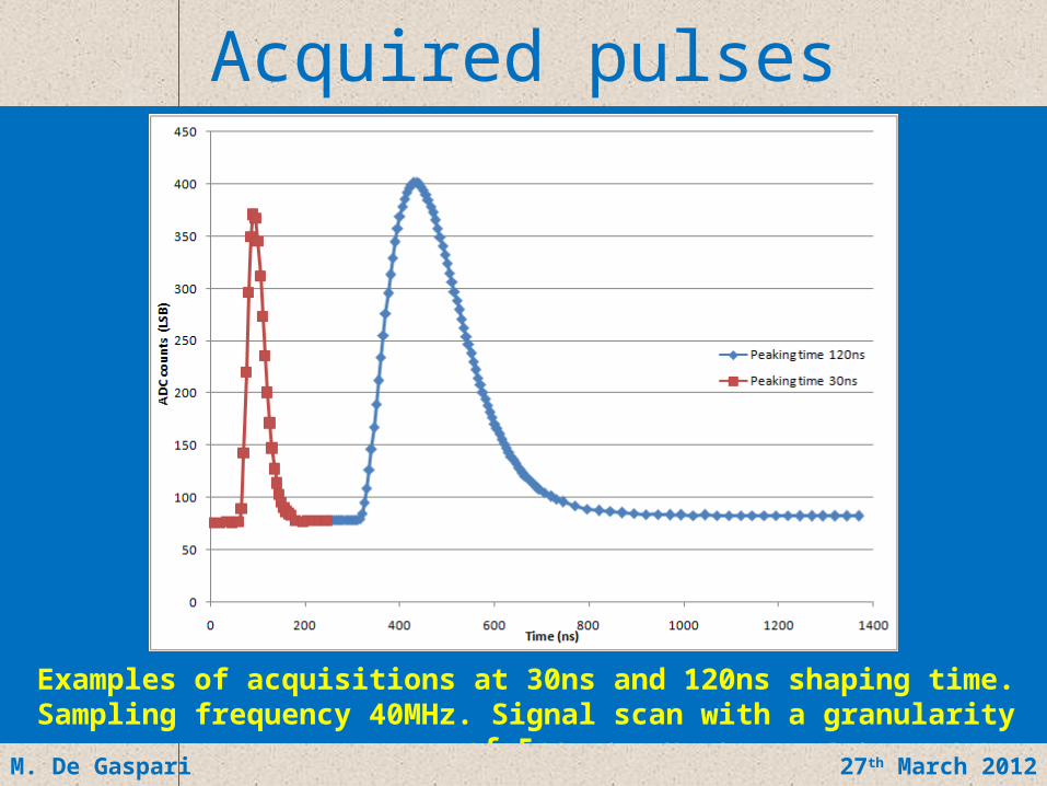
New test conditions: Sampling clock frequency increased to 40MHz (design target), readout
clock 40MHz. Chip PGA3: the inputs of the PASA are not bonded. This avoids noise
injection from the ground plane of the test board. Chip PGA4: all inputs bonded.
Measurements presented today: Analog noise Digital power consumption Chip power consumption and power pulsing measurements
LC Power Distribution & Pulsing Workshop, May 201122nd November 2011M. De Gaspari 27th March 2012
Config 120ns L 12 120ns L 27 30ns L 12 30ns L 27 120ns H 12 30ns H 12
PGA3
Noise LSB 0.480 0.655 0.526 0.683 0.498 0.504
Noise fC 0.088 0.051 0.103 0.059 0.092 0.100
Noise e- 547 316 641 370 574 625
PGA4
Noise LSB 0.709 1.346 1.475 3.263 0.668 1.279
Noise fC 0.129 0.104 0.287 0.283 0.123 0.254
Noise e- 809 649 1796 1768 770 1587
LC Power Distribution & Pulsing Workshop, May 201122nd November 2011M. De Gaspari 27th March 2012
Baseline noise: PGA4
Measured baseline noise for different input capacitances.
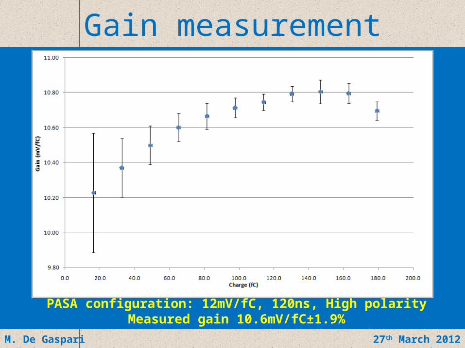
PGA4, Channel 0, 120ns, 12mV/fC
LC Power Distribution & Pulsing Workshop, May 201122nd November 2011M. De Gaspari 27th March 2012
Baseline noise: DSP influence
Negligible influence of the amount of switching logic on the noise: basic data acquisition and data acquisition with BC1 memory (Look-Up Table) switching.
LC Power Distribution & Pulsing Workshop, May 201122nd November 2011M. De Gaspari 27th March 2012
(PGA4)
DSP tests 1
Emulates the pattern produced by a real detector
Known pattern written in the Pedestal Memory (Baseline Correction 1) and used as test input
Undershoots
Drift of the baseline
LC Power Distribution & Pulsing Workshop, May 201122nd November 2011M. De Gaspari 27th March 2012
DSP tests 2
The DSP removes offsets, undershoots, baseline drifts
LC Power Distribution & Pulsing Workshop, May 201122nd November 2011M. De Gaspari 27th March 2012
Power consumption: DSP
Power consumption of the DSP when acquiring at 40MHz sampling frequency. Different DSP functionalities included.
LC Power Distribution & Pulsing Workshop, May 201122nd November 2011M. De Gaspari 27th March 2012
Power consumption: DSP
Power consumption of the DSP for different sampling clock frequencies.DSP configuration: (Data In) – (Look-Up Table).
LC Power Distribution & Pulsing Workshop, May 201122nd November 2011M. De Gaspari 27th March 2012
Power consumption: DSP
Power consumption of the DSP at different supply voltages.Efficient operation down to 1V supply.
LC Power Distribution & Pulsing Workshop, May 201122nd November 2011M. De Gaspari 27th March 2012
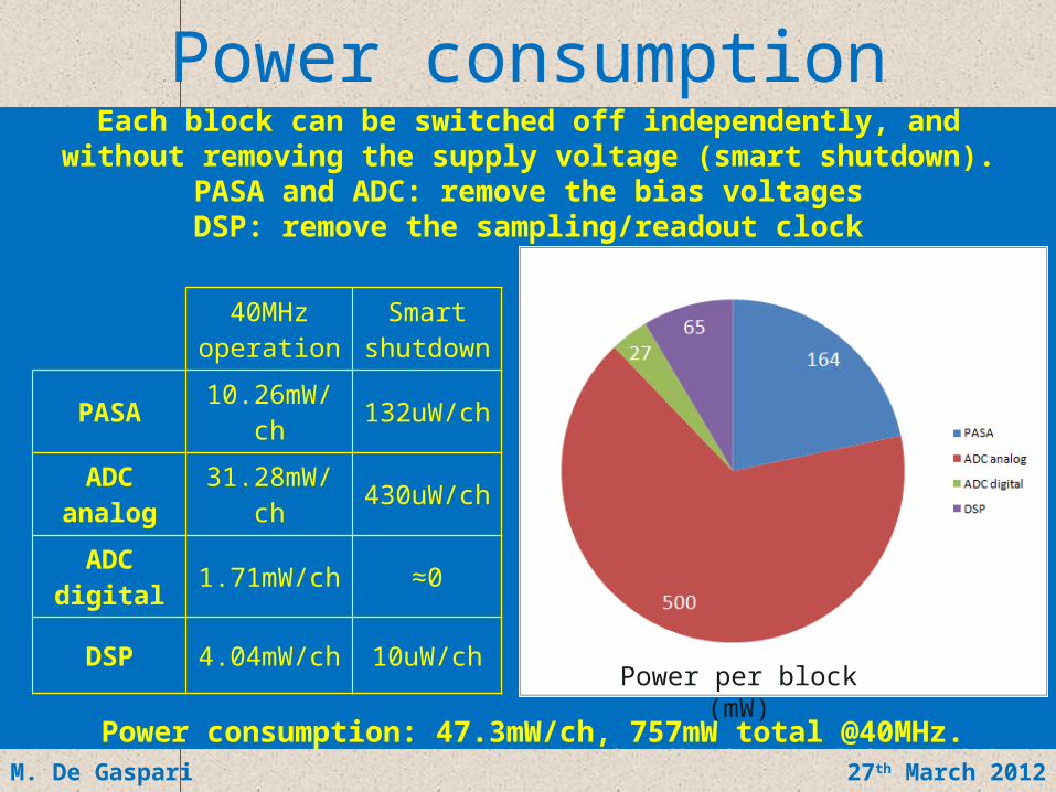
Power consumption
40MHzoperation
Smartshutdown
PASA 10.26mW/ch 132uW/ch
ADC analog 31.28mW/ch 430uW/ch
ADC digital 1.71mW/ch ≈0
DSP 4.04mW/ch 10uW/ch
Power per block (mW)
Power consumption: 47.3mW/ch, 757mW total @40MHz.LC Power Distribution & Pulsing Workshop, May 201122nd November 2011M. De Gaspari 27th March 2012
Each block can be switched off independently, and without removing the supply voltage (smart shutdown).
PASA and ADC: remove the bias voltagesDSP: remove the sampling/readout clock
Power pulsing cycleAcquisition Readout
Power up L1 Trigger
Power consumption of the DSP during a power pulsing cycle.
Minimum delay between power up and L1 trigger has to be measured.Readout time is determined by the test setup (RCU) minimum PP cycle ≈1ms.
LC Power Distribution & Pulsing Workshop, May 201122nd November 2011M. De Gaspari 27th March 2012
Power pulsing cycle
A test pulse is injected after power up; the amplitude of the pulse is monitored with different delays between power up and L1.
100usec delay gives good results: difference with continuous mode <1LSB
Good region Continuous mode
LC Power Distribution & Pulsing Workshop, May 201122nd November 2011M. De Gaspari 27th March 2012
Power pulsing: results
Power pulsing cycles are repeated at a frequency of 50Hz (Duty≈1/20).Chip total power=9.2mW+50Hz*654.3uJ=41.9mW
Power reduction by a factor 18.1!(continuous mode: 757mW)
Shutdown (mW) Power pulsing cycle (uJ)
PASA 2.12 145.2
ADC analog 6.88 421.1
ADC digital 0.01 22.9
DSP 0.16 58.3
Pads ≈0 6.9
Total 9.2 654.3
LC Power Distribution & Pulsing Workshop, May 201122nd November 2011M. De Gaspari 27th March 2012
Conclusions
LC Power Distribution & Pulsing Workshop, May 201122nd November 2011
• The 16 channel Super-ALTRO Demonstrator has been designed, prototyped and tested successfully!!
• The chip is already usable for the Linear Collider TPC prototype.The area is 3.07mm2/channel (LCTCP requirement: <4mm2)
• Using appropriate design techniques, integration of low-noise analog components and digital functions is possible with little effect on noise performance.
• Power pulsing approach has been demonstrated effective in reducing the power consumption, while preserving the performance.