Page 1
mSATA SJ2 Datasheet
Rev 1.0 Nov 2014 Page 1
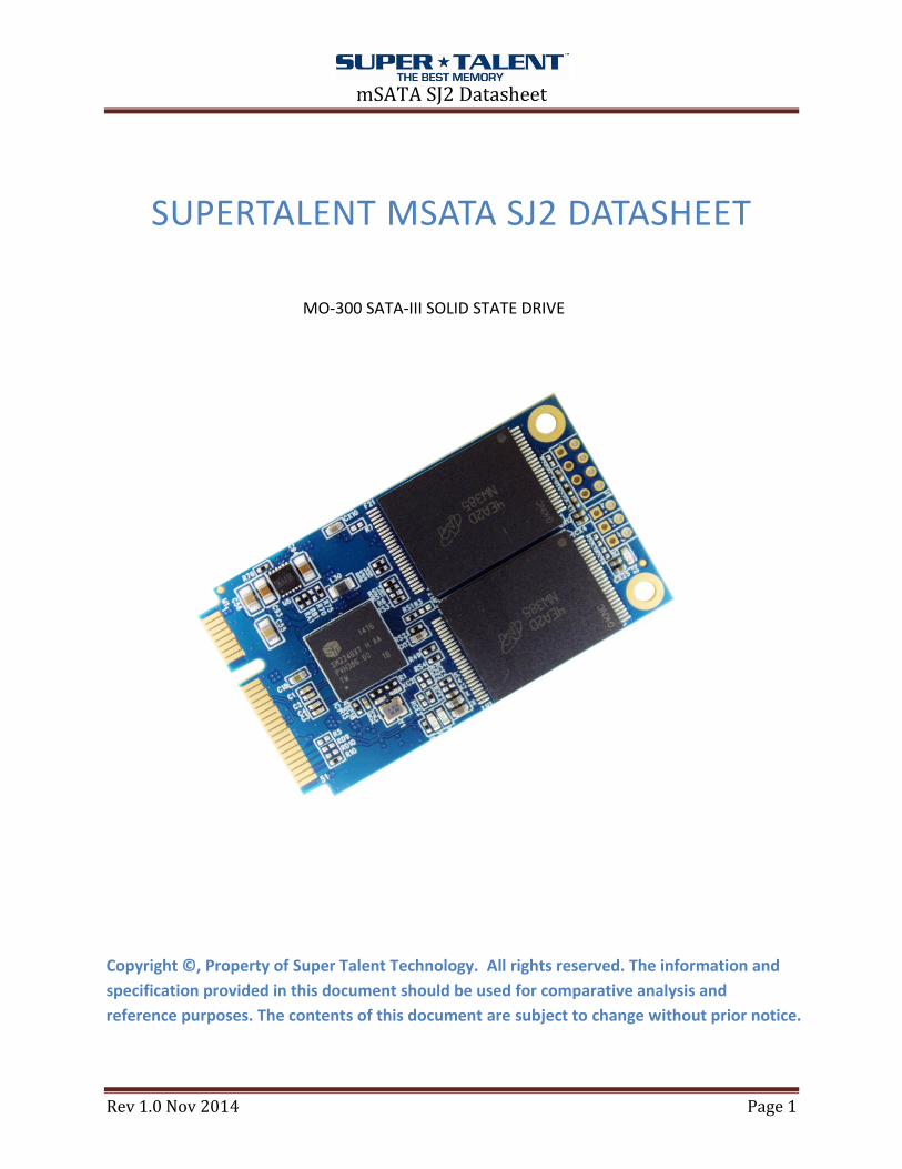
SUPERTALENT MSATA SJ2 DATASHEET
MO-300 SATA-III SOLID STATE DRIVE
Copyright © , Property of Super Talent Technology. All rights reserved. The information and
specification provided in this document should be used for comparative analysis and
reference purposes. The contents of this document are subject to change without prior notice.
Page 2
mSATA SJ2 Datasheet
Rev 1.0 Nov 2014 Page 2
TABLE OF CONTENTS
Table of Figures ............................................................................................................................... 3
Table of Tables ................................................................................................................................ 3
1.0 Product Description .................................................................................................................. 5
1.1 Product Overview ................................................................................................................. 5
1.2 Target Applications ............................................................................................................... 5
1.3 Product Features ................................................................................................................... 5
1.4 System Requirements ........................................................................................................... 6
2.0 Product Ordering Part Numbers ............................................................................................... 6
2.1 Ordering Part Structure ........................................................................................................ 6
2.2 Valid Ordering Part Numbers ................................................................................................ 7
3.0 Physical Specifications .............................................................................................................. 7
3.1 Mechanical Specifications (PCBA) ......................................................................................... 7
4.0 Electrical Specifications ............................................................................................................. 8
4.1 Performance Specifications .................................................................................................. 8
4.2 Power And Temperature Conditions .................................................................................... 8
4.3 Power Consumption Test For Result .................................................................................... 9
5.0 Environmental Specifications ................................................................................................... 9
6.0 Quality And Reliability Specifications ....................................................................................... 9
7.0 Compliance Specifications ...................................................................................................... 10
8.0 Pin Descriptions ...................................................................................................................... 10
8.1 Mini SATA Interface Drawing .............................................................................................. 10
8.2 Pin Signals Assignments ...................................................................................................... 11
Page 3
mSATA SJ2 Datasheet
Rev 1.0 Nov 2014 Page 3
9.0 Supported ATA Command Set ................................................................................................ 11
9.1 ATA Command Register ...................................................................................................... 11
9.2 Identify Device Command Information .............................................................................. 13
9.3 Supported Identify Device command Information Definitions .......................................... 16
10 Installation............................................................................................................................... 17
10.1 Before Getting Started ...................................................................................................... 17
10.2 Installation ........................................................................................................................ 17
10.3 Using The SSD.................................................................................................................... 17
For More Information ................................................................................................................... 18
Change Record .............................................................................................................................. 18
TABLE OF FIGURES
Figure 1: Outline Drawing ............................................................................................................... 7
Figure 2: Interface Description ..................................................................................................... 10
TABLE OF TABLES
Table 1: Ordering Part Structure ..................................................................................................... 6
Table 2: Valid Ordering Part Numbers ............................................................................................ 7
Table 3: Data Transfer Time Specifications .................................................................................... 8
Table 4: Absolute Maximum Ratings .............................................................................................. 8
Table 5: Power Consumption Test For Result ................................................................................. 9
Table 6: Compatibility Test Config ................................................................................................ 10
Table 7: Pin Assignment ................................................................................................................ 11
Table 8: Command Set .................................................................................................................. 11
Table 9: Set Features Register Values ........................................................................................... 13
Page 4
mSATA SJ2 Datasheet
Rev 1.0 Nov 2014 Page 4
Table 10: Identify Device Command Definition Abbreviation Decoder ....................................... 13
Table 11: Identify Device Table Information ................................................................................ 14
Table 12: SMART Data Vendor-specific Attributes ....................................................................... 16
Table 13: Change Record .............................................................................................................. 18
Page 5
mSATA SJ2 Datasheet
Rev 1.0 Nov 2014 Page 5
1.0 PRODUCT DESCRIPTION
1.1 PRODUCT OVERVIEW
The introduction of the mSATA SJ2 is full consists of semiconductor devices using NAND flash
memory which provide high reliability and high performance for a storage media. And opens up
some very exciting possibilities for the Industrial and Commercial storage market. The mSATA
SJ2 are substantially smaller, lighter weight and consume less power compared to hard drives,
yet have sufficient storage space to load an O/S and serve as a bootable drive for embedded
applications. Moreover, these devices have excellent resistance to shock, vibration, dust,
temperature extremes and other environmental hazards.
mSATA SJ2 which features outstanding performance. Available in 16GB to 256GB capacities,
this drives electrically complied with the SATA-II/SATA-III standards and is electrically
compatible with a serial ATA disk drive. The transmission speed of up to 480MB/s.
Measuring 50.80mm x 29 .85mm x 3.50mm, the mSATA SJ2 is very small in volume and Super
Speed, it can match and satisfy different customer‘s demand. It can easily mount on notebook
without any cable, and provides fast read and writes speed, high reliability it an ideal storage
solution for the server and mobile environment.
1.2 TARGET APPLICATIONS
Military and Aerospace
Embedded / Industrial Systems
Medical Industry
Notebook
Casino Gaming
1.3 PRODUCT FEATURES
Capacity: 16GB ,32GB, 64GB, 128GB ,256GB
Form Factor: mini PCIe (50.80mm x 29 .85mm x 3.50mm)
Reliable MLC or SLC NAND type flash
Electrically fully complied with the SATA-II/SATA-III standards
Data retention: JESD47 compliant
S.M.A.R.T. command transport (SCT) technology
Enhanced endurance by dynamic/static wear-leveling.
Hardware BCH ECC 66bits in 1,024 bytes.
Data integrity under power-cycling.
Page 6
mSATA SJ2 Datasheet
Rev 1.0 Nov 2014 Page 6
Spec meet JEDEC MO-300.
100% tested HW and SW.
1.4 SYSTEM REQUIREMENTS
Operating Voltage Requirement: Vcc = 3.3V +/-5%
Operating System: Supported by all operating systems
Interface: SATA 3.0Gbps (SATA‐II), SATA 6.0Gbps (SATA‐III)
Installation Requirements:
System Hardware which supports SATA-II/SATA-III standards
System Hardware includes mSATA socket or transfer board
2.0 PRODUCT ORDERING PART NUMBERS
2.1 ORDERING PART STRUCTURE
Table 1: Ordering Part Structure
Product Type X
Density XXX
Technology XX
Form & Case Factor XX
F – Channel MD – mSATA SLC Full Size 30x50 016 – 16GB MT – SM2246XT SATA
3.0 (no DRAM) 4CH RM – Board Only
M5 – mSATA MLC Full Size 30x50 032 – 32GB
064 – 64GB
128 – 128GB
256 – 256GB
Page 7
mSATA SJ2 Datasheet
Rev 1.0 Nov 2014 Page 7
2.2 VALID ORDERING PART NUMBERS
Table 2: Valid Ordering Part Numbers
Product Family Capacity Flash Mode Encryption Channel/Retail Part
Number
mSATA SJ2
16GB SLC Commercial FMD016MTRM
MLC Commercial FM5016MTRM
32GB SLC Commercial FMD032MTRM
MLC Commercial FM5032MTRM
64GB SLC Commercial FMD064MTRM
MLC Commercial FM5064MTRM
128GB MLC Commercial FM5128MTRM
256GB MLC Commercial FM5256MTRM
3.0 PHYSICAL SPECIFICATIONS
3.1 MECHANICAL SPECIFICATIONS (PCBA)
Length: 50.80 ± 0.25 mm
Width: 29.85± 0.25 mm
Thickness: 3.50 ± 0.25 mm
Figure 1: Outline Drawing
Page 8
mSATA SJ2 Datasheet
Rev 1.0 Nov 2014 Page 8
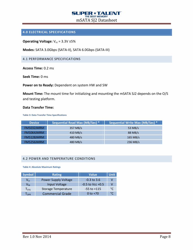
4.0 ELECTRICAL SPECIFICATIONS
Operating Voltage: Vcc = 3.3V ±5%
Modes: SATA 3.0Gbps (SATA‐II), SATA 6.0Gbps (SATA‐III)
4.1 PERFORMANCE SPECIFICATIONS
Access Time: 0.2 ms
Seek Time: 0 ms
Power on to Ready: Dependent on system HW and SW
Mount Time: The mount time for initializing and mounting the mSATA SJ2 depends on the O/S
and testing platform.
Data Transfer Time:
Table 3: Data Transfer Time Specifications
Device Sequential Read Max (MB/Sec) * Sequential Write Max (MB/Sec) *
FM5032JMRM 357 MB/s 53 MB/s FM5064JMRM 410 MB/s 88 MB/s FM5128JMRM 480 MB/s 165 MB/s FM5256JMRM 480 MB/s 236 MB/s
4.2 POWER AND TEMPERATURE CONDITIONS
Table 4: Absolute Maximum Ratings
Symbol Rating Value Unit
Vcc Power Supply Voltage -0.3 to 3.6 V VIN Input Voltage -0.5 to Vcc +0.5 V
TSTG Storage Temperature -55 to +115 °C
TOPR Commercial Grade 0 to +70 °C
Page 9
mSATA SJ2 Datasheet
Rev 1.0 Nov 2014 Page 9
4.3 POWER CONSUMPTION TEST FOR RESULT
Table 5: Power Consumption Test For Result
Test software: Crystal Disk Mark3.0
Times 1 2 3 Power(W=U*I)
Static current(Idle mode current) 100mA 100mA 100mA 3.3V*0.100A=0.330W
Dynamic current (R/W mode
current)
Seq read 340mA 340mA 340mA 3.3V*0.340A=1.122W
Seq write 180mA 180mA 180mA 3.3V*0.180A=0.594W
512K read 280mA 280mA 280mA 3.3V*0.280A=0.924W
512K write 380mA 380mA 380mA 3.3V*0.380A=1.254W
4K read 170mA 170mA 170mA 3.3V*0.155A=0.561W
4K write 240mA 240mA 240mA 3.3V*0.247A=0.792W
4K QD32 read 170mA 170mA 170mA 3.3V*0.155A=0.561W
4K QD32 write 240mA 240mA 240mA 3.3V*0.247A=0.792W
5.0 ENVIRONMENTAL SPECIFICATIONS
Operating Temperature:
Commercial Grade: 0°C to +70°C
Humidity: 5% to ~98% RH
Operating Shock: 1500G
Operating Vibration: 16G
Operating Altitude: TBD
6.0 QUALITY AND RELIABILITY SPECIFICATIONS
Data Retention: JESD47 compliant
Wear Leveling: Dynamic and static wear-leveling
Bad Block Management: Drive will self identify bad blocks and remap physical to logical
addresses to avoid bad blocks.
Page 10
mSATA SJ2 Datasheet
Rev 1.0 Nov 2014 Page 10
ECC/EDC (Error Correction Code/Error Detection Code): Built in error detection and correction
will correct physical bit errors in NAND. Drives use BCH 66 bits ECC
MTBF: >1,000,000 hours
Power Cycle:
Table 6: Compatibility Test Config
Test Platform: Compatibility Test Config
Test Items Total Times PASS Times Fail Times Log Photo
Cycles 1000 times 1000 times 0 times
Suspend 1000 times 1000 times 0 times
7.0 COMPLIANCE SPECIFICATIONS
All mSATA SJ2 are compliant with the following standards and regulations:
RoHS
CE
FCC
8.0 PIN DESCRIPTIONS
8.1 MINI SATA INTERFACE DRAWING
Interface Description (mSATA)
Figure 2: Interface Description
Page 11
mSATA SJ2 Datasheet
Rev 1.0 Nov 2014 Page 11
8.2 PIN SIGNALS ASSIGNMENTS
Table 7: Pin Assignment
9.0 SUPPORTED ATA COMMAND SET
9.1 ATA COMMAND REGISTER
mSATA SJ2 supports the command show in the following tables.
Table 8: Command Set
Command Name Code (Hex) Protocol
General Feature Set
Execute Device Diagnostic 90h Execute device diagnostic
Pin Signal Name Description Pin Signal Name Description
1 Reserved NC 2 +3.3V 3.3V Power (Source)
3 Reserved NC 4 GND Return Current Path
5 Reserved NC 6 VCC1.5 NC
7 Reserved NC 8 Reserved NC
9 GND Return Current Path 10 Reserved NC
11 Reserved NC 12 Reserved NC
13 Reserved NC 14 Reserved NC
15 GND Return Current Path 16 Reserved NC
17 Reserved NC 18 GND Return Current Path
19 Reserved NC 20 Reserved NC
21 GND Return Current Path 22 Reserved NC
23 TX+ SATA transmitter differential pair
24 +3.3V VAUX3.3
25 TX- 26 GND Return Current Path
27 GND Return Current Path 28 VCC1.5 NC
29 GND Return Current Path 30 SMB_CLK NC
31 RX- SATA receiver differential pair
32 SMB_DATA NC
33 RX+ 34 GND Return Current Path
35 GND Return Current Path 36 USB_DN NC
37 GND Ground 1st
mate 38 USB_DP NC
39 +3.3V 3.3V Power (Source) 40 GND Return Current Path
41 +3.3V 3.3V Power (Source) 42 Reserved NC
43 Device Type Return Current Path/NC 44 Devslp Device Sleep Mode
45 Reserved FORCE-ROM(TX)/NC 46 Reserved NC
47 Reserved SATA LED (RX)/NC 48 VCC1.5 NC
49 DA/DSS Device Activity Signal 50 GND Return Current Path
51 GND Return Current Path 52 +3.3V 3.3V Power (Source)
Page 12
mSATA SJ2 Datasheet
Rev 1.0 Nov 2014 Page 12
Command Name Code (Hex) Protocol
Flush Cache E7h Non-data
Identify Device ECh PIO data-in
Initialize Drive Parameters 91h Non-data
Read DMA C8h DMA
Read Log Ext 2Fh PIO data-in
Read Multiple C4h PIO data-in
Read Sector(s) 20h PIO data-in
Read Verify Sector(s) 40h or 41h Non-data
Set Feature EFh Non-data
Set Multiple Mode C6h Non-data
Write DMA CAh DMA
Write Multiple C5h PIO data-out
Write Sector(s) 30h PIO data-out
NOP 00h Non-data
Read Buffer E4h PIO data-in
Write Buffer E8h PIO data-out
Power Management Feature Set
Check Power Mode E5h or 98h Non-data
Idle E3h or 97h Non-data
Idle Immediate E1h or 95h Non-data
Sleep E6h or 99h Non-data
Standby E2h or 96h Non-data
Standby Immediate E0h or 94h Non-data
Security Mode Feature Set
Security Set Password F1h PIO data-out
Security Unlock F2h PIO data-out
Security Erase Prepare F3h Non-data
Security Erase Unit F4h PIO data-out
Security Freeze Lock F5h Non-data
Security Disable Password F6h PIO data-out
SMART Feature Set
SMART Disable Operations B0h Non-data
SMART Enable/Disable Autosave B0h Non-data
SMART Enable Operations B0h Non-data
SMART Execute OFF-LINE Immediate B0h Non-data
SMART Read Log B0h PIO data-in
SMART Read Data B0h PIO data-in
SMART Read Threshold B0h PIO data-in
SMART Return Status B0h Non-data
SMART Save Attribute Values B0h Non-data
SMART Write Log B0h PIO data-out
Host Protected Area Feature Set
Page 13
mSATA SJ2 Datasheet
Rev 1.0 Nov 2014 Page 13
Command Name Code (Hex) Protocol
Read Native Max Address F8h Non-data
Set Max Address F9h Non-data
Set Max Set Password F9h PIO data-out
Set Max Lock F9h Non-data
Set Max Freeze Lock F9h Non-data
Set Max Unlock F9h PIO data-out
48-bit Address Feature Set
Flush Cache Ext EAh Non-data
Read Sector(s) Ext 24h PIO data-out
Read DMA Ext 25h DMA
Read Multiple Ext 29h PIO data-out
Read Native Max Address Ext 27h Non-data
Read Verify Sector(s) Ext 42h Non-data
Set Max Address Ext 37h Non-data
Write DMA Ext 35h DMA
Write Multiple Ext 39h PIO data-out
Write Sector(s) Ext 34h PIO data-out
NCQ Feature Set
Read FPDMA Queued 60h DMA Queued
Write FPDMA Queued 61h DMA Queued
Others
Data Set Management 06h DMA
Seek 70h Non-data
Table 9: Set Features Register Values
Value Command Value Command
D0h Read Data D5h Read Log
D1h Read Attribute Threshold D6h Write Log
D2h Enable/Disable Autosave D8h Enable SMART Operations
D3h Save Attribute Values D9h Disable SMART Operations
D4h Execute OFF-LINE Immediate DAh Return Status
Note: If the reserved size is below the threshold, the status can be read from the Cylinder
Register using the Return Status command (DAh).
9.2 IDENTIFY DEVICE COMMAND INFORMATION
Table 10: Identify Device Command Definition Abbreviation Decoder
Parameter Definition
F/V Fixed/Variable Content F Content (byte) is fixed and does not change.
Page 14
mSATA SJ2 Datasheet
Rev 1.0 Nov 2014 Page 14
V Content (byte) is variable and may change depending on the state of the device or the commands executed by the device.
X Content (byte) is vendor specific and may be fixed or variable.
Table 11: Identify Device Table Information
Word Value F/V Description
0 044Ah F General configuration
1 XXXXh X Default number of cylinders
2 0000h V Reserved
3 00XXh X Default number of heads
4 0000h X Obsolete
5 0240h X Obsolete
6 XXXXh F Default number of sectors per track
7-8 XXXXh V Number of sectors per card (Word 7 = MSW, Word 8 = LSW)
9 0000h X Obsolete
10-19 XXXXh F Serial number in ASCII (Right justified)
20 0002h X Obsolete
21 0002h X Obsolete
22 0000h X Obsolete
23-26 XXXXh F Firmware revision in ASCII Big Endian Byte Order in Word
27-46 XXXXh F Model number in ASCII (Left justified) Big Endian Byte Order in Word
47 8001h F Maximum number of sectors on Read/Write Multiple command
48 0000h F Reserved
49 0300h F Capabilities
50 4000h F Capabilities
51 0200h F PIO data transfer cycle timing mode
52 0000h X Obsolete
53 0007h F Field validity
54 XXXXh X Current numbers of cylinders
55 XXXXh X Current numbers of heads
56 XXXXh X Current sectors per track
57-58 XXXXh X Current capacity in sectors (LBAs) (Word 57 = LSW , Word 58 = MSW)
59 0101h F Multiple sector setting
60-61 XXXXh F Total number of user addressable logical sectors for 28-bit commands (DWord)
62 0000h X Reserved
63 0207h F Multiword DMA transfer Supports MDMA mode 0, 1 and 2
Page 15
mSATA SJ2 Datasheet
Rev 1.0 Nov 2014 Page 15
Word Value F/V Description
64 0003h F Advanced PIO modes supported
65 0078h F Minimum Multiword DMA transfer cycle time per word
66 0078h F Recommended Multiword DMA transfer cycle time
67 0078h F Minimum PIO transfer cycle time without flow control
68 0078h F Minimum PIO transfer cycle time with lORDY flow control
69 4000h F Additional supported
70-74 0000h F Reserved
75 001Fh F Queue depth
76 030Eh F
Serial ATA capabilities • Supports Serial ATA Gen3 • Supports Serial ATA Gen2 • Supports Serial ATA Gen1 • Supports Phy event counters log • Supports receipt of host initiated power management requests • Supports Native Command Queuing
77 0080h F Serial ATA additional capability • DevSleep_to_ReducedPwerState
78 0148h F
Serial ATA features supported • Supports Device Sleep • Supports • Software settings preservation • Device supports initiating power management
79 0040h V Reserved
80 03FCh F Major version number (ACS-2)
81 0000h F Minor version number
82 702Bh F Command sets supported 0
83 7500h F Command sets supported 1
84 4002h F Command sets supported 2
85-87 XXXXh V Command set/feature enabled
88 007Fh V Ultra DMA mode supported and selected
89 0003h F Time required for a Normal Erase mode Security Erase Unit command
90 0001h F Time required for an Enhanced Erase mode Security Erase Unit command
91 0000h V Current advanced power management value
92 FFFEh V Master password identifier
93-99 0000h V Reserved
100-103 XXXXh V Maximum user LBA for 48-bit address feature set
104 0000h V Reserved
105 0100h F Maximum number of 512-byte blocks per Data Set Management command
106-127 0000h V Reserved
128 0009h V Security status
129-159 XXXXh X Vendor specific
160 0000h F CFA power mode
Page 16
mSATA SJ2 Datasheet
Rev 1.0 Nov 2014 Page 16
Word Value F/V Description
161 0000h X Reserved
162 0000h F Key management schemes supported
163 0000h F CF Advanced True lDE Timing mode capability and setting
164-168 0000h V Reserved
169 0001h F Data Set Management supported
170-216 XXXXh V Reserved
217 0001h F Non-rotating media (SSD)
218-221 0000h X Reserved
222 107Fh F Transport major revision (SATA Rev 3.1)
223-254 0000h X Reserved
255 XXXXh X Integrity word
9.3 SUPPORTED IDENTIFY DEVICE COMMAND INFORMATION DEFINITIONS
Table 12: SMART Data Vendor-specific Attributes
Attribute ID(Hex)
Raw Attribute Value Attribute Name
01 MSB 00 00 00 00 00 Read error rate
05 LSB MSB 00 00 00 00 Reallocated sectors count
09 LSB MSB 00 00 Reserved
0C LSB MSB 00 00 Power cycle count
A0 LSB MSB 00 00 Uncorrectable sector count when read/write
A1 LSB MSB 00 00 00 00 Number of valid spare block
A2 LSB MSB 00 00 00 00 Number of cache data block
A3 LSB MSB 00 00 00 00 Number of initial invalid block
A4 LSB MSB 00 00 Total erase count
A5 LSB MSB 00 00 Maximum erase count
A6 LSB MSB 00 00 Minimum erase count
A7 LSB MSB 00 00 Average erase count
C0 LSB MSB 00 Power-off retract count
C2 MSB 00 00 00 00 00 Controlled temperature
C3 LSB MSB 00 00 Hardware ECC recovered
C4 LSB MSB 00 00 Reallocation event count
C7 LSB MSB 00 00 00 00 UltraDMA CRC error count
F1 LSB MSB 00 00 Total LBAs written (each write unit=32MB)
F2 LSB MSB 00 00 Total LBAs read (each read unit=32MB)
Page 17
mSATA SJ2 Datasheet
Rev 1.0 Nov 2014 Page 17
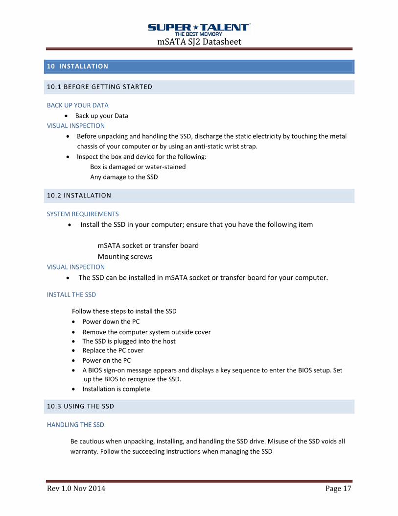
10 INSTALLATION
10.1 BEFORE GETTING STARTED
BACK UP YOUR DATA
Back up your Data
VISUAL INSPECTION
Before unpacking and handling the SSD, discharge the static electricity by touching the metal
chassis of your computer or by using an anti-static wrist strap.
Inspect the box and device for the following:
Box is damaged or water-stained
Any damage to the SSD
10.2 INSTALLATION
SYSTEM REQUIREMENTS
Install the SSD in your computer; ensure that you have the following item
mSATA socket or transfer board
Mounting screws
VISUAL INSPECTION
The SSD can be installed in mSATA socket or transfer board for your computer.
INSTALL THE SSD
Follow these steps to install the SSD
Power down the PC
Remove the computer system outside cover
The SSD is plugged into the host
Replace the PC cover
Power on the PC
A BIOS sign-on message appears and displays a key sequence to enter the BIOS setup. Set up the BIOS to recognize the SSD.
Installation is complete
10.3 USING THE SSD
HANDLING THE SSD
Be cautious when unpacking, installing, and handling the SSD drive. Misuse of the SSD voids all
warranty. Follow the succeeding instructions when managing the SSD
Page 18
mSATA SJ2 Datasheet
Rev 1.0 Nov 2014 Page 18
Follow all ESD pre-cautions always operate the SSD within environmental conditions never
switch DC power to the drive by plugging and Ensure correct interface polarity whenever
plugged into the drive
FOR MORE INFORMATION
For Technical Support:
If additional support is needed, please visit the Super Talent Web site at www.supertalent.com
for the following topics:
Warranty Services: Includes the warranty service policy and the RMA request forms.
Technical Information: Includes product data sheets and various USB whitepapers.
Tools Section: Includes frequently asked questions (FAQs).
For More Information or Further Technical Support Please Contact:
Super Talent Technology 2077 North Capitol Avenue San Jose, CA 95132 USA Tel: +1 (408) 934-2560 Support: [email protected] Sales: [email protected] OEM Sales: [email protected]
CHANGE RECORD
Table 13: Change Record
Version Release Date Changes
1.0 November 21st , 2014 Initial Release in new template