1
1
2 Supplementary Information:
3
4
5 Semi-Transparent Perovskite Films with Centimeter-Scale Superior Uniformity
6 by the Hybrid Deposition Method7
8 Luis K. Ono ᵻ, Shenghao Wang ᵻ, Yuichi Kato, Sonia R. Raga, Yabing Qi*
9 Energy Materials and Surface Sciences Unit, Okinawa Institute of Science and Technology
10 Graduate University, 1919-1 Tancha Onna-son, Okinawa 904-0495 Japan.
11 *E-mail: [email protected]
12 ᵻ Luis K. Ono and Shenghao Wang contributed equally to this work.
13
14
15 Contents:
16
17 1. Experimental section. (page 2)
18
19 2. Hybrid deposition system, side and top view descriptions. (page 7)
20
21 3. Time evolution of evaporation rates read by QCMs. (page 8)
22
23 4. Perovskite thickness determination by AFM. (page 9)
24
25 5. Optical microscope images. (page 10)
26
27 6. The complete set of J-V characteristics of ~50 nm and ~135 nm perovskite solar cells.
28 (page 11)
29
30 7. Hysteresis effects. (page 12)
31
Electronic Supplementary Material (ESI) for Energy & Environmental Science.This journal is © The Royal Society of Chemistry 2014
2
32 Experimental Section.
33
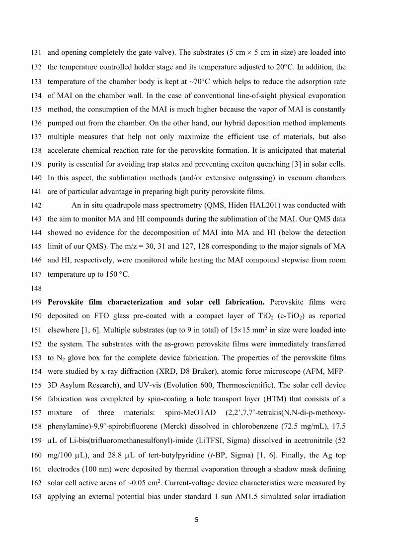
34 Instrumentation details. The overall side-view of the hybrid deposition system is displayed
35 in Fig. 1a and S1. Additional top-views at the different cross sections of the instrument are
36 displayed in Fig. S1. The main vacuum chamber (customized system, Part #1 in Fig. 1a) is
37 evacuated by a pumping system (Part #2) which consists of a turbo molecular pump
38 (HiPace300, Pfeiffer), manual gate-valve (10840-CE01, VAT). The substrate holder stage
39 (Part #3) allows stable cooling and heating in the temperature range from 190C up to
40 200C. The system can accommodate a wide range of substrate (Part #4) sizes (up to 5 cm5
41 cm). The substrate shutter (Part #5) is mounted on a push-pull linear motion device (MDC)
42 just below the substrate. The evaporation rates are monitored by two QCMs (Inficon, Parts #6
43 and #7). The first QCM (Part #6) is facing downward which monitors the PbCl2 (received
44 from Aldrich and used without further purification) evaporation rate while the second QCM
45 (Part #7) facing upward is used to monitor the MAI vapor only. Two evaporation sources are
46 needed for the perovskite film formation. Vapor of MAI is produced by a Knudsen cell (K-
47 cell, Part #8) type source (KOD-Cell, Kitano Seiki) to fill the chamber. AlN crucibles
48 containing MAI (1 cc volume) are resistively heated by applying current through a heating
49 element which surrounds the crucible. The second component, PbCl2 is resistively heated
50 from a large dish-shaped crucible (Part #9) to provide large scale uniform evaporation. The
51 heating element (Part #10) consists of a tungsten wire (=0.25 mm) wound into a spiral shape
52 and connected to commercially available power supply (30 A/36 V) through electric
53 feedthroughs (Part #11). The halide shutter (Part #12) is mounted on a linear motion device
54 enabling independent calibration of the evaporation rate of MAI. The total pressure inside the
55 chamber is monitored by a full-range (1105 ~ 1107 Pa) pressure gauge (Crystal/Cold
56 cathode gauge from R-DEC, Part #13).
57 Initially, the MAI QCM (Part#7) parameters were set to density (1.0 g/cm3) and
58 acoustic impedance (1.0) as reported previously [1, 2]. However, we were unable to calibrate
59 our quartz crystal parameters (tooling factor) by the standard ways of measuring the thickness
60 of deposited MAI film by AFM or profilometer. We have observed that MAI film growths as
61 patches (islands) instead of a uniform flat film even on a flatter surface of silicon with native
62 oxide. Thus, an alternative procedure similar to the one reported by Malinkiewicz et al. [3]
63 and Polander et al. [4] has been conducted. Note that similarly they were also unable to
64 determine the MAI thickness quantitatively in their systems. Our methodology is based on
3
65 the MAI vapor pressure inside the chamber. Because the QCM that monitors MAI faces
66 upwards (Part#7) in our system, we set the QCM parameters so the signal-to-noise ratio was
67 reasonable for monitoring the MAI during evaporation. The optimized parameters were
68 =0.2 g/cm3; Z-factor = 0.2; Tooling = 100. Thus, the MAI QCM (Part#7) in our system also
69 serves to monitor indirectly the MAI time evolution during heating and perovskite formation
70 (see Fig. S2), but cannot quantify the absolute MAI amount inside the chamber. We have
71 optimized the perovskite deposition conditions by preparing several batches of perovskite
72 films prepared with a varied MAI nominal rates to identify the evaporation conditions that
73 give strong diffraction peaks in X-ray diffraction (XRD, Fig. 2a) corresponding to the
74 perovskite structure and at the same time give the minimal diffraction peak intensities for
75 non-perovskite related phases (e.g. MAI).
76 The eventual excess of MAI on perovskites was observed to show detrimental device
77 performance. Thus, we have analyzed carefully the possible origins for generating the non-
78 stoichiometric perovskite films in our system and our methodology. The excess of MAI could
79 be monitored by XRD measurements showing the characteristic 10 and 20 diffraction peaks.
80 The following issues were detected as possible sources for generating excess of MAI in our
81 system and were circumvented: (i) during the warm up of the MAI crucible until the nominal
82 evaporation rate is attained, deposition of MAI on the substrate can occur. Although the
83 sample shutter (Figs. 1 and S1, Part#5) is kept closed at all times until the perovskite
84 deposition is started, the MAI was found to be volatile and thus, can deposit on the substrate.
85 Our system was designed to have a load-lock chamber coupled to the hybrid deposition
86 chamber and isolated by a gate-valve (10840-CE01, VAT). During warm up of the MAI and
87 PbCl2 crucibles, the sample holder carrying the large substrate (55 cm2) is stored in the load-
88 lock and avoids the MAI exposure. Only when the nominal rates are achieved, the sample
89 holder is in situ transferred from the load-lock to the evaporation chamber by a magnetic
90 transfer rod. The sample transfer operation takes less than 3 minutes; (ii) large variations of
91 MAI pressure during perovskite deposition can generate sample with excess of MAI. A
92 relatively high pressure of 0.3 Pa (~2.3 mTorr) is needed for the perovskite formation in our
93 system. This high pressure is kept constant all the time during perovskite deposition by using
94 the Knudsen-cell (Part#8, Fig. 1 and S1) that allows precise temperature control. In addition,
95 the manual gate-valve (Part#2) is set to a predetermined opening position and minimum valve
96 operation is required to keep the pressure (0.3 Pa) constant during perovskite deposition; (iii)
97 The generation of the MAI vapor is not ceased immediately when the MAI heating element is
4
98 stopped because it takes a substantial period of time for the crucible to cool down. Thus, the
99 remaining unknown concentration of MAI in the chamber generates perovskite films with
100 topmost layers with different stoichiometric compositions (MAI:PbCl2). After the completion
101 of the deposition, the sample is immediately transferred from the deposition chamber to the
102 load-lock chamber to minimize the excessive deposition of MAI on top of the perovskite
103 films.
104
105 Methylammonium iodide synthesis. MAI was synthesized according to a literature
106 procedure with slight modification [5]. Briefly, hydroiodic acid solution was gradually added
107 to methyl amine ethanol solution that was kept stirring in an ice-bath. Ethanol and water from
108 the mixed solution was evaporated using a rotary evaporator (BUCHI, Rotavapor R-3). The
109 precipitated yellow-colored crystals were dissolved in hot ethanol, and cooled in a
110 refrigerator at 5 C for recrystallization. Subsequently, the crystals were filtered and washed
111 with tetrahydrofuran resulting in white crystal powder. We dried and kept the MAI in N2
112 glove box (<0.1 ppm of O2 and H2O).
113
114 Perovskite film deposition. The growth of perovskite films in our system is based on the
115 concept of controlling the MAI vapor pressure and flow that fills the entire vacuum chamber.
116 The K-cell (Part #8) produces well controllable amounts of the MAI vapor that is further
117 controlled by the gate-valve (Part #2). A shutter in front of the K-cell is kept closed at all
118 times to avoid the high flux of MAI hitting directly the substrate area. This is critical because
119 the deposition only via MAI pressure ensures uniformity. Perovskite films are formed by a
120 chemical reaction between the PbCl2 deposited onto the substrate (that has good sticking
121 coefficient, uniformity, wettability, and nicely forms the line-of-sight molecular beam
122 according to the cosine law) and the MAI from the gas-phase (vapor). Because of the
123 directionality nature of the lead halide deposition, the use of widely-open dish-shaped
124 crucible surrounded by a spiral-shaped filament is essential for producing uniform
125 evaporation rates of the lead halide across the entire substrate surface area. The high
126 crystallinity through the entire film thickness is produced by a good control of the MAI vapor
127 pressure and a stable lead halide evaporation rate. The gate-valve allows the control of the
128 MAI vapor pressure inside the chamber (i.e., setting the gate-valve to a predetermined
129 opening position can help hold the MAI vapor in the chamber during perovskite deposition)
130 as well as to precisely stop the perovskite reaction at any time (by stopping the MAI heating
5
131 and opening completely the gate-valve). The substrates (5 cm 5 cm in size) are loaded into
132 the temperature controlled holder stage and its temperature adjusted to 20C. In addition, the
133 temperature of the chamber body is kept at ~70C which helps to reduce the adsorption rate
134 of MAI on the chamber wall. In the case of conventional line-of-sight physical evaporation
135 method, the consumption of the MAI is much higher because the vapor of MAI is constantly
136 pumped out from the chamber. On the other hand, our hybrid deposition method implements
137 multiple measures that help not only maximize the efficient use of materials, but also
138 accelerate chemical reaction rate for the perovskite formation. It is anticipated that material
139 purity is essential for avoiding trap states and preventing exciton quenching [3] in solar cells.
140 In this aspect, the sublimation methods (and/or extensive outgassing) in vacuum chambers
141 are of particular advantage in preparing high purity perovskite films.
142 An in situ quadrupole mass spectrometry (QMS, Hiden HAL201) was conducted with
143 the aim to monitor MA and HI compounds during the sublimation of the MAI. Our QMS data
144 showed no evidence for the decomposition of MAI into MA and HI (below the detection
145 limit of our QMS). The m/z = 30, 31 and 127, 128 corresponding to the major signals of MA
146 and HI, respectively, were monitored while heating the MAI compound stepwise from room
147 temperature up to 150 C.
148
149 Perovskite film characterization and solar cell fabrication. Perovskite films were
150 deposited on FTO glass pre-coated with a compact layer of TiO2 (c-TiO2) as reported
151 elsewhere [1, 6]. Multiple substrates (up to 9 in total) of 1515 mm2 in size were loaded into
152 the system. The substrates with the as-grown perovskite films were immediately transferred
153 to N2 glove box for the complete device fabrication. The properties of the perovskite films
154 were studied by x-ray diffraction (XRD, D8 Bruker), atomic force microscope (AFM, MFP-
155 3D Asylum Research), and UV-vis (Evolution 600, Thermoscientific). The solar cell device
156 fabrication was completed by spin-coating a hole transport layer (HTM) that consists of a
157 mixture of three materials: spiro-MeOTAD (2,2’,7,7’-tetrakis(N,N-di-p-methoxy-
158 phenylamine)-9,9’-spirobifluorene (Merck) dissolved in chlorobenzene (72.5 mg/mL), 17.5
159 L of Li-bis(trifluoromethanesulfonyl)-imide (LiTFSI, Sigma) dissolved in acetronitrile (52
160 mg/100 L), and 28.8 L of tert-butylpyridine (t-BP, Sigma) [1, 6]. Finally, the Ag top
161 electrodes (100 nm) were deposited by thermal evaporation through a shadow mask defining
162 solar cell active areas of ~0.05 cm2. Current-voltage device characteristics were measured by
163 applying an external potential bias under standard 1 sun AM1.5 simulated solar irradiation
6
164 (100 mW/cm2, Newport Oriel Sol1A) and measuring the photocurrent generated (Keithley
165 2420 source meter). Typical voltage scan on our devices was performed starting from +1.1 V
166 to 0.2 V (Forward). Prior to the first scan, pre-illumination under the solar simulator was
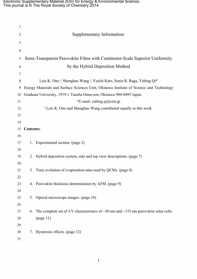
167 performed for 30 seconds. It has been observed that more stable J-V curves with less
168 hysteresis effects are obtained when the cells are illuminated prior to the J-V measurements.
169 The scan rate was fixed at 0.15 Vs1. External quantum efficiency (EQE) was recorded as a
170 function of wavelength on the complete devices (Newport Oriel IQE-200).
171
7
172
4 3 5
8
2
6
1
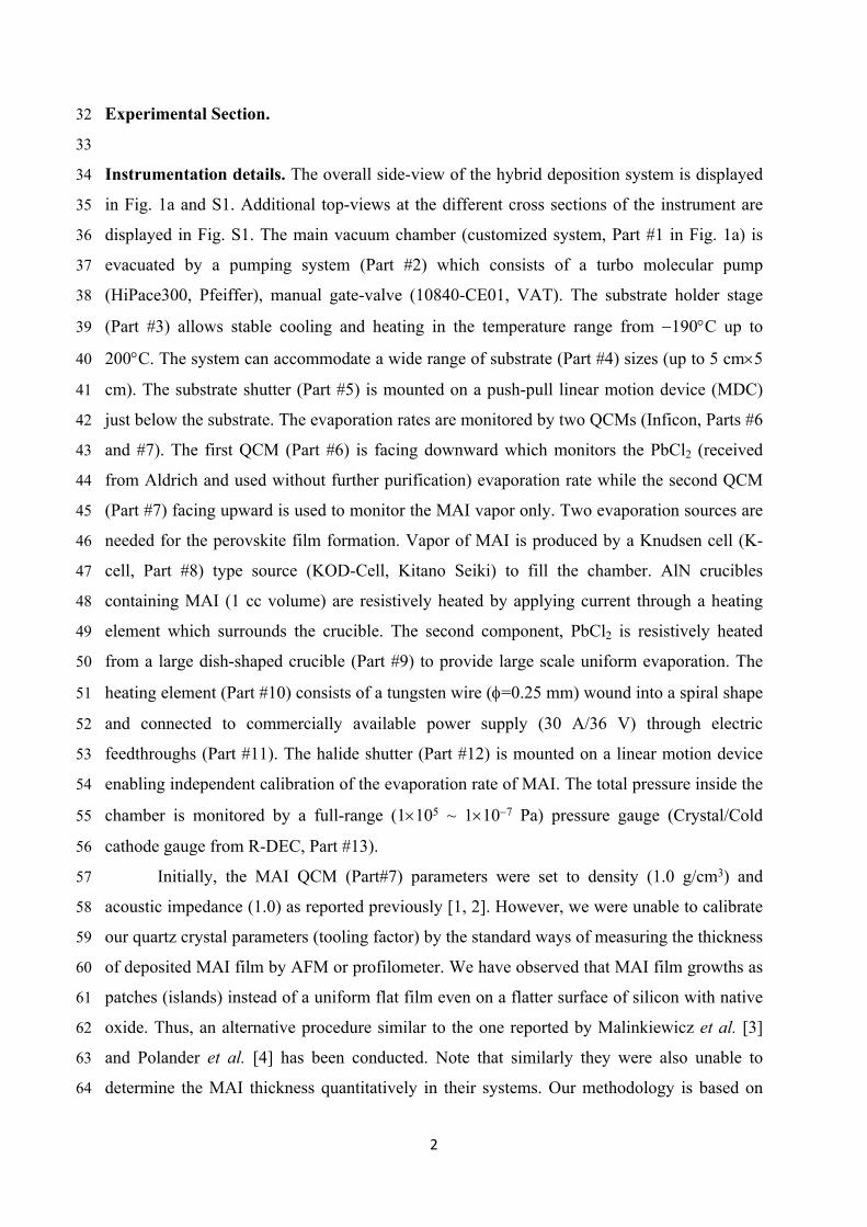
9
X X’
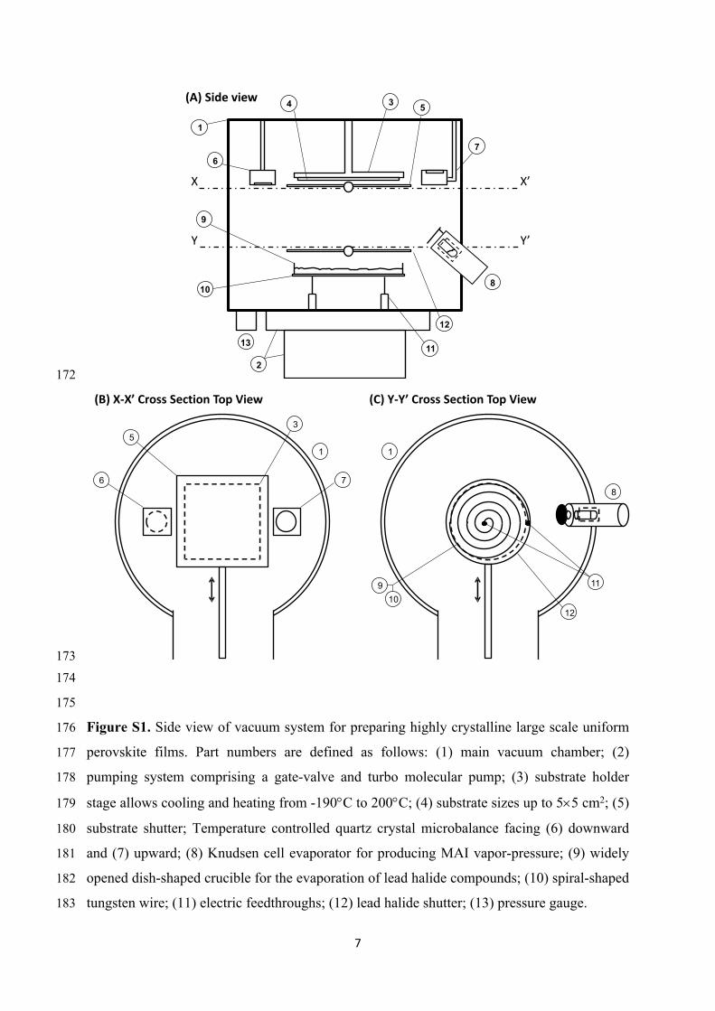
Y Y’
(A) Side view
7
10
1113
12
173
35
6 7
(B) X-X’ Cross Section Top View
12
9
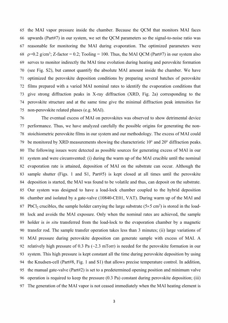
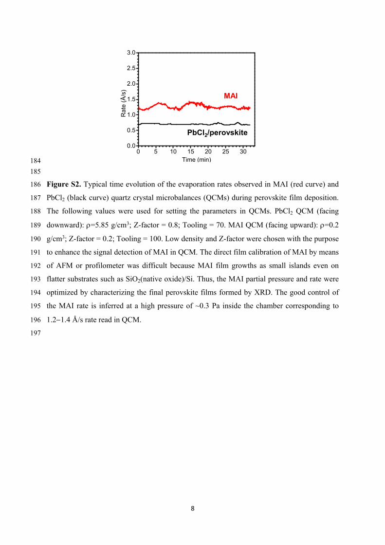
8
(C) Y-Y’ Cross Section Top View
1 1
10
11
174
175
176 Figure S1. Side view of vacuum system for preparing highly crystalline large scale uniform
177 perovskite films. Part numbers are defined as follows: (1) main vacuum chamber; (2)
178 pumping system comprising a gate-valve and turbo molecular pump; (3) substrate holder
179 stage allows cooling and heating from -190C to 200C; (4) substrate sizes up to 55 cm2; (5)
180 substrate shutter; Temperature controlled quartz crystal microbalance facing (6) downward
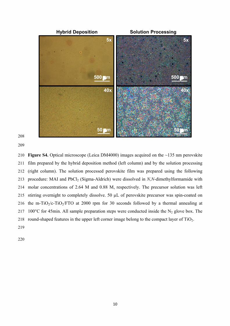
181 and (7) upward; (8) Knudsen cell evaporator for producing MAI vapor-pressure; (9) widely
182 opened dish-shaped crucible for the evaporation of lead halide compounds; (10) spiral-shaped
183 tungsten wire; (11) electric feedthroughs; (12) lead halide shutter; (13) pressure gauge.
8
1840 5 10 15 20 25 30
0.0
0.5
1.0
1.5
2.0
2.5
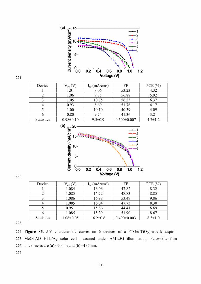
3.0
Rat
e (Å
/s)
Time (min)
PbCl2/perovskite
MAI
185
186 Figure S2. Typical time evolution of the evaporation rates observed in MAI (red curve) and
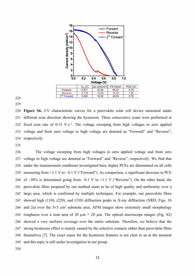
187 PbCl2 (black curve) quartz crystal microbalances (QCMs) during perovskite film deposition.
188 The following values were used for setting the parameters in QCMs. PbCl2 QCM (facing
189 downward): =5.85 g/cm3; Z-factor = 0.8; Tooling = 70. MAI QCM (facing upward): =0.2
190 g/cm3; Z-factor = 0.2; Tooling = 100. Low density and Z-factor were chosen with the purpose
191 to enhance the signal detection of MAI in QCM. The direct film calibration of MAI by means
192 of AFM or profilometer was difficult because MAI film growths as small islands even on
193 flatter substrates such as SiO2(native oxide)/Si. Thus, the MAI partial pressure and rate were
194 optimized by characterizing the final perovskite films formed by XRD. The good control of
195 the MAI rate is inferred at a high pressure of ~0.3 Pa inside the chamber corresponding to
196 1.21.4 Å/s rate read in QCM.
197
9
198
199
240 nm
8 7
56 4
23 1
9
245 nm
(a) (b) (c)Position 5 (center) Position 8 (edge)
200
201 Figure S3. Tapping mode AFM images (scan size: 90 16 m2) showing the edge between
202 perovskite film and substrate generated by covering half of the sample with a shadow mask.
203 (a) Sample positions were numbered as indicated over the 55 cm2 total area. AFM
204 measurements were conducted (b) at the center and (c) at one edge on a large-scale 55 cm2
205 area. The corresponding height-profiles (averaged across the vertical direction) are shown
206 below the images (b) and (c).
207
10
208
5x
40x
5x
40x
Hybrid Deposition Solution Processing
500 m500 m
50 m50 m
209
210 Figure S4. Optical microscope (Leica DM4000) images acquired on the ~135 nm perovskite
211 film prepared by the hybrid deposition method (left column) and by the solution processing
212 (right column). The solution processed perovskite film was prepared using the following
213 procedure: MAI and PbCl2 (Sigma-Aldrich) were dissolved in N,N-dimethylformamide with
214 molar concentrations of 2.64 M and 0.88 M, respectively. The precursor solution was left
215 stirring overnight to completely dissolve. 50 µL of perovskite precursor was spin-coated on
216 the m-TiO2/c-TiO2/FTO at 2000 rpm for 30 seconds followed by a thermal annealing at
217 100°C for 45min. All sample preparation steps were conducted inside the N2 glove box. The
218 round-shaped features in the upper left corner image belong to the compact layer of TiO2.
219
220
11
221
0.0 0.2 0.4 0.6 0.8 1.0 1.20
5
10
15
1 2 3 4 5 6
Voltage (V) C
urre
nt d
ensi
ty (m
A/cm
2 )(a)
Device Voc (V) Jsc (mA/cm2) FF PCE (%)1 1.01 8.06 53.23 4.32 2 1.06 9.85 56.88 5.92 3 1.05 10.75 56.23 6.37 4 0.93 8.69 51.76 4.17 5 1.00 10.10 40.39 4.09 6 0.80 9.74 41.36 3.21
Statistics 0.980.10 9.50.9 0.5000.007 4.71.2
222
0.0 0.2 0.4 0.6 0.8 1.0 1.20
5
10
15
20
Voltage (V)
Cur
rent
den
sity
(mA/
cm2 )
1 2 3 4 5 6
(b)
Device Voc (V) Jsc (mA/cm2) FF PCE (%)1 1.084 16.06 47.82 8.32 2 1.085 16.72 48.83 8.85 3 1.086 16.98 53.49 9.86 4 1.085 16.04 47.73 8.30 5 0.951 15.86 44.41 6.69 6 1.085 15.39 51.90 8.67
Statistics 1.060.05 16.20.6 0.4900.003 8.51.0223
224 Figure S5. J-V characteristic curves on 6 devices of a FTO/c-TiO2/perovskite/spiro-
225 MeOTAD HTL/Ag solar cell measured under AM1.5G illumination. Perovskite film
226 thicknesses are (a) ~50 nm and (b) ~135 nm.
227
12
228
0.0 0.2 0.4 0.6 0.8 1.002468
1012141618
Voltage (V)
Forward Reverse 2nd Forward
Curr
ent d
ensi
ty (m
A/cm
2 )
Voc (V) Jsc (mA/cm2) Fill Factor PCE (%)Forward 0.871 16.39 40.47 5.78 Reverse 0.718 15.55 16.29 1.82
2nd Forward 0.862 16.50 40.63 5.78
229
230 Figure S6. J-V characteristic curves for a perovskite solar cell device measured under
231 different scan direction showing the hysteresis. Three consecutive scans were performed at
232 fixed scan rate of 0.15 Vs1. The voltage sweeping from high voltages to zero applied
233 voltage and from zero voltage to high voltage are denoted as “Forward” and “Reverse”,
234 respectively.
235
236 The voltage sweeping from high voltages to zero applied voltage and from zero
237 voltage to high voltage are denoted as “Forward” and “Reverse”, respectively. We find that
238 under the measurement conditions investigated here, higher PCEs are determined on all cells
239 measuring from +1.1 V to 0.1 V (“Forward”). As comparison, a significant decrease in PCE
240 of ~30% is determined going from 0.1 V to +1.1 V (“Reverse”). On the other hand, the
241 perovskite films prepared by our method seem to be of high quality and uniformity over a
242 large area, which is confirmed by multiple techniques. For example, our perovskite films
243 showed high (110), (220), and (330) diffraction peaks in X-ray diffraction (XRD, Figs. 1b
244 and 2a) over the 55 cm2 substrate area. AFM images show extremely small morphology
245 roughness over a scan area of 20 m × 20 µm. The optical microscope images (Fig. S2)
246 showed a very uniform coverage over the entire substrate. Therefore, we believe that the
247 strong hysteresis effect is mainly caused by the selective contacts rather than perovskite films
248 themselves [7]. The exact cause for the hysteresis features is not clear to us at the moment
249 and this topic is still under investigation in our group.
250
13
251 References
252
253 [1] M.Z. Liu, M.B. Johnston, and H.J. Snaith, Efficient planar heterojunction perovskite solar cells by
254 vapour deposition. Nature 501 (2013) 395-398.
255 [2] A.S. Subbiah, A. Halder, S. Ghosh, N. Mahuli, G. Hodes, and S.K. Sarkar, Inorganic Hole
256 Conducting Layers for Perovskite-Based Solar Cells. J. Phys. Chem. Lett. 5 (2014) 1748-1753.
257 [3] O. Malinkiewicz, A. Yella, Y.H. Lee, G.M. Espallargas, M. Graetzel, M.K. Nazeeruddin, and H.J.
258 Bolink, Perovskite solar cells employing organic charge-transport layers. Nat. Photonics 8 (2014)
259 128-132.
260 [4] L.E. Polander, P. Pahner, M. Schwarze, M. Saalfrank, C. Koerner, and K. Leo, Hole-transport
261 material variation in fully vacuum deposited perovskite solar cells. APL Mater. 2 (2014) 081503.
262 [5] M.M. Lee, J. Teuscher, T. Miyasaka, T.N. Murakami, and H.J. Snaith, Efficient Hybrid Solar
263 Cells Based on Meso-Superstructured Organometal Halide Perovskites. Science 338 (2012) 643-
264 647.
265 [6] Q. Chen, H. Zhou, Z. Hong, S. Luo, H.-S. Duan, H.-H. Wang, Y. Liu, G. Li, and Y. Yang, Planar
266 heterojunction perovskite solar cells via vapor-assisted solution process. J. Am. Chem. Soc. 136
267 (2013) 622-625.
268 [7] H.J. Snaith, A. Abate, J.M. Ball, G.E. Eperon, T. Leijtens, N.K. Noel, S.D. Stranks, J.T.-W. Wang,
269 K. Wojciechowski, and W. Zhang, Anomalous Hysteresis in Perovskite Solar Cells. J. Phys.
270 Chem. Lett. 5 (2014) 1511-1515.
271


![Supporting Information · Haiyang Chemical Co. Ltd silica gel 60 (200-300mesh). The rotavapor was BUCHI’s Rotavapor R-3. General procedure for benzanilides preparation[3] A mixture](https://static.documents.pub/doc/80x56/600a6b5ddf00c36679728d31/supporting-haiyang-chemical-co-ltd-silica-gel-60-200-300mesh-the-rotavapor-was.jpg)


