Determination of the temperature-dependent cell membranepermeabilities using microfluidics with integrated flow and
temperature controlCifeng Fang,a Fujun Ji,a,b Zhiquan Shu,∗a,c and Dayong Gao∗a
a Department of Mechanical Engineering, University of Washington, Seattle, WA 98195, USA.b School of Information, Capital University of Economics and Business, Beijing 100070, China.
c School of Mechanical and Materials Engineering, Washington State University, Everett, WA 98201, USA
Supplementary Movies
Movie S1 Shows cell volume historical during media switching from 1x PBS to 3x PBS at room temperature, 30 ◦ and 37 ◦. This clipwas captured at 30 fps for 60 secs and plays at 60 fps. Scale bar: 20 µm)Movie S2 Shows cell volume historical during media switching from 1x PBS to 10% (v/v) DMSO at room temperature, 30 ◦ and 37 ◦.This clip was captured at 30 fps for 180 secs and plays at 180 fps. Scale bar: 20 µm)
MicrofabricationWe use standard multilayered soft-lithography (MSL) protocols for fabrication the microfluidic channel and the wet etching process forconductive wire micropatterning (see Result section). The mask design is also available as a separate file in ESI.
Conductive wire patterning
A glass slide (EMF, CA-134) with a 1000 Å thick gold film on a 50 Å thick chrome adhesion layer was used for conductive wirepatterning. The slide was spincoated with a positive photoresist with thickness ∼ 1.5 µm (Microchem, AZ-1512), followed by a softbaking process at 110 ◦C for 2 min. The microheater and the adjacent temperature sensor were designed by AutoCAD and printedon a transparency with 50,800 dpi resolution (Fineline Imaging, OR). The exposure process was carried out by using a mask aligner(ABM-aligner, ABM-USA Inc.) under wavelength of 365 µm for 5–6 sec. The photoresist was then developed by using 25 % v/v aqueousphotoresist solution (Microchem, AZ-340) for 1 min. The glass slide with the patterned photoresist was baked at 110 ◦C for 1 hr forbetter adhesion and curing. A wet etching process was conducted by immersing the glass slide into gold etchant (TFA gold etchant,Transene) for 30–35 sec, followed by immersing the glass slide immediately in chrome etchant (TFE chromium etchant, Transene) for2–3 sec. The glass slide was rinsed by acetone to remove residual photoresist. The etched glass slide was again rinsed with isopropanol(IPA) and water, and dried by nitrogen gas. The glass slide, together with the electric connection pads covered by Teflon tape, wascoated with 100 nm silicon dioxide to prevent any electrolysis.
Double layered microchannel fabrication
The microfluidic channel was fabricated using standard multilayer soft-lithography (MSL). Photomasks were designed using AutoCADand printed on a transparency with 50,800 dpi resolution using commercial laser photoplotting service (Fineline Imaging, OR). Themasters were fabricated by contact photolithography using a negative photoresist (SU-8 2050, Microchem). The photoresist wasspincoated onto a plasma-cleaned 100 mm silicon wafer (test grade wafer, SVM). After a soft baking process at 65 ◦C for 3 minthen at 95 ◦C for 9 min, an exposure process was carried out by using a mask aligner (ABM-USA Inc., ABM-aligner) with a 365 µmwavelength UV light for 22 sec. After post baking (2 min at 65 ◦C, 7 min at 95 ◦C), the master was then developed with a propyleneglycol monomethyl ether acetate (PGMEA) (Y020100, Microchem), followed by surface treatment with trichloro (1H, 1H, 2H, 2H-perfluorooctyl) silane (448931, Sigma-Aldrich) vapor under a vacuum condition for easy peeling of PDMS replica from the master.Two SU-8 masters of fluidic layer (70 µm deep) and control layer (70 µm deep) were fabricated. The fluid layer with a thin PDMSvalve membrane was obtained by spincoating the fluidic SU-8 master with PDMS (Sylgard 184, Dow Corning) at 15:1 ratio of thebase resin and the crosslinker. The control layer was fabricated by casting PDMS at 5:1 ratio of base resin and crosslinker onto thecorresponding SU-8 master. Both PDMS layers were partially cured by baking at 65 ◦C for 25 min. The thick PDMS replica (controllayer) was then peeled off from the master, aligned, and was hermetically sealed onto the thin PDMS layer (fluidic layer). The bondedPDMS double-layer was placed on a hot plate at 65 ◦C for 4 hr to form an integrated monolithic device.
• Make sure by microscope that the sharp face of the trans-parency should be faced to gold slide directly, exposure 5-6s.
• 4:1 ratio of water : AZ 340 for 1mins, after develop, putslides into water and rinse.
• Post bake 110 ◦C for 1 hour.
• Wet etching:
– Gold etching: 30-35s
– Chrome etching: 1-2s
– Water rinsing
• Put patterned slides into acetone for 2 hours
• Rinse slide(s) with
– IPA - Water - IPA
– Dry with N2
Deposit silicon oxide layer to slides:
• Clean patterned slide (s), rinse with
– Acetone - IPA - Water - IPA
– Dry with N2
• Cover the connection pads with Teflon types.
• Mount slides to sample holder and place to deposition cham-ber.
• Deposit silicon oxide layer.
• Peel off the Teflon tapes.
Bonding:
• Remove fluidic layer master/PDMS/Control layer PDMS slabfrom oven and let cool.
• Use scalpel to cut along the control PDMS edge to removeboth layers.
• Chop excess PDMS edges with razor blade, separate each de-vice, and hole punch inlet ports in the fluidic layer.
• Clean PDMS with tape and clean patterned slide(s) withdeionized (DI) H2O. Then rinse with IPA.
• Dry patterned slide(s) with N2 and place on metal plate sam-ple holder next to PDMS slab that sits side up
• Place into the chamber of plasma cleaner (Harrick Plasma,PDC-32G), set the RF level to MED and after reaching be-tween 500 mTorr -1Torr run for 90 s allowing a small amountof air into the chamber every 30 s.
• When time is up, remove and immediately bond to the pat-terned slide by placing one edge at desired location anddropping the slab to force air out, then put the bonded deviceon the hot plate (65 ◦C) baking for 1 hour –overnight.
3
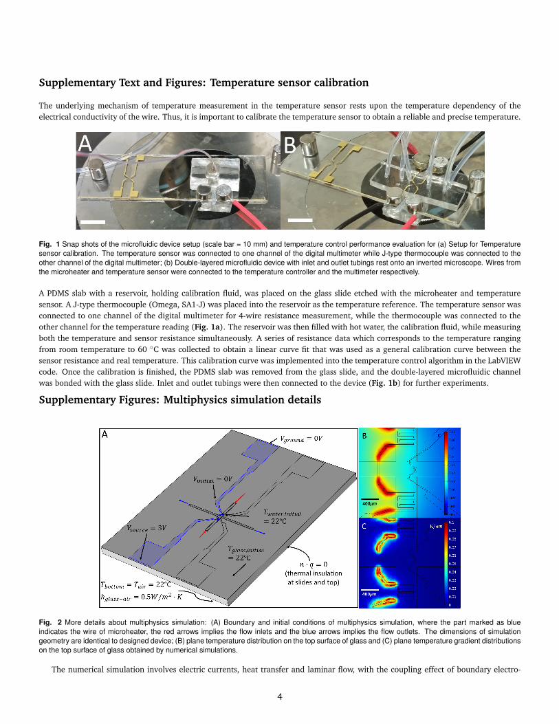
Supplementary Text and Figures: Temperature sensor calibration
The underlying mechanism of temperature measurement in the temperature sensor rests upon the temperature dependency of theelectrical conductivity of the wire. Thus, it is important to calibrate the temperature sensor to obtain a reliable and precise temperature.
Fig. 1 Snap shots of the microfluidic device setup (scale bar = 10 mm) and temperature control performance evaluation for (a) Setup for Temperaturesensor calibration. The temperature sensor was connected to one channel of the digital multimeter while J-type thermocouple was connected to theother channel of the digital multimeter; (b) Double-layered microfluidic device with inlet and outlet tubings rest onto an inverted microscope. Wires fromthe microheater and temperature sensor were connected to the temperature controller and the multimeter respectively.
A PDMS slab with a reservoir, holding calibration fluid, was placed on the glass slide etched with the microheater and temperaturesensor. A J-type thermocouple (Omega, SA1-J) was placed into the reservoir as the temperature reference. The temperature sensor wasconnected to one channel of the digital multimeter for 4-wire resistance measurement, while the thermocouple was connected to theother channel for the temperature reading (Fig. 1a). The reservoir was then filled with hot water, the calibration fluid, while measuringboth the temperature and sensor resistance simultaneously. A series of resistance data which corresponds to the temperature rangingfrom room temperature to 60 ◦C was collected to obtain a linear curve fit that was used as a general calibration curve between thesensor resistance and real temperature. This calibration curve was implemented into the temperature control algorithm in the LabVIEWcode. Once the calibration is finished, the PDMS slab was removed from the glass slide, and the double-layered microfluidic channelwas bonded with the glass slide. Inlet and outlet tubings were then connected to the device (Fig. 1b) for further experiments.
Fig. 2 More details about multiphysics simulation: (A) Boundary and initial conditions of multiphysics simulation, where the part marked as blueindicates the wire of microheater, the red arrows implies the flow inlets and the blue arrows implies the flow outlets. The dimensions of simulationgeometry are identical to designed device; (B) plane temperature distribution on the top surface of glass and (C) plane temperature gradient distributionson the top surface of glass obtained by numerical simulations.
The numerical simulation involves electric currents, heat transfer and laminar flow, with the coupling effect of boundary electro-
4
magnetic heat source and non-isothermal flow. The details about the boundary and initial conditions are showed in Fig. 2A. Fig. 2B andC demonstrate the plane temperature profile on the top surface of glass.
Supplementary Figures: Cell image analysis
Fig. 3 Cell volume excursion under 10% (v/v) DMSO perfusing at 22◦C. The result raw images before image processing and the segmented cell masksare also showed above the analysis result plotting.
Supplementary Table: The osmolalities of perfusion solutions used in experiment
Table 1 The osmolalities of perfusion solutions used in experiment
Supplementary Text and Figures: Sphericity ananlysis of processed cell images
To evaluate the how well the sphere cell shape assumption is across the cell volume changing, we involves the sphericity, which wasdefined as 2π · requ/pact . Here, requ is the equivalent cell radius calculated with the two-dimensional cell area based on spherical cellshape assumption, and pact is the perimeter of the obtained two-dimensional mask of trapped cell. As showed in Fig. 4, the cellsphericities excursion during perfusion by hypertionic solutions are generally above 0.9, at some worst cases it reaches around 0.7,which indicates that, for Jurkat cells, the spherical cell shape assumption fits the actual experiment situation fairly well.
Supplementary Text and Figures: LabVIEW program
Hardware componentsAll the hardware components were real time controlled with a custom made LabVIEW program. The hardware is not limited to specificbuild up. Components from other venders will also work after proper modification of hardware Input/Output (I/O) setup in LabVIEW.
Real time image processingThe LabVIEW built-in Vision Assistant Express module was used for image processing, involving the feature enhancement and particleanalysis. The real time image processing for cell segmentation is challenging, as the illumination condition of cell change dynamically.
5
Fig. 4 The cell sphericity excursion during perfusion by hypertonic solutions at various temperature: The left column: 1×PBS to 3×PBS at 22◦C, 30◦C,37◦C; The right column: 1×PBS to 10% (v/v) DMSO at 22◦C, 30◦C, 37◦C.
To achieve optimized results, we incorporate the following functions: threshold, thin, fill holes, removal of small objects and particleanalysis. See example image processing sequence showed in Fig. 5, from raw images to particle detection.
Fig. 5 Image processing sequence: The image was first threshold to show mainly the outline of cell; Then by several steps of morphology enhancement(thin, fill holes and remove small objects), the cell feature was segmented as cell mask, the particle analysis was conducted to result cell mask and thecentroid and area of cell can by obtained, which can be use for the cell trapping feedback control.