+ All Categories
Home > Documents > Supplementary Material (ESI) for Energy & Environmental...

Supplementary Material (ESI) for Energy & Environmental...

Date post: 29-Jun-2018
Category:
Upload: danghuong
View: 219 times
Download: 0 times
Share this document with a friend
7
M. C. Putnam, S. W. Boettcher, M. D. Kelzenberg, D. B. Turner-Evans, J. M. Spurgeon, E. L. Warren, R. M. Briggs, N. S. Lewis, and H. A. Atwater, Si Microwire-Array Solar Cells, 2010. 1 Si Microwire-Array Solar Cells -- Supporting Information Ag Back Reflector: Figure S1 provides scanning electron microscope (SEM) images that document the fabrication of a Ag back reflector. Following two 500 nm Ag evaporations Ag uniformly coated the substrate and the wire sidewalls (Fig. S1A). PDMS was then deposited and continuously coated the Ag‐coated substrate (Fig. S1A,B). (Because the SEM images shown are from the edge of a wire array, the PDMS is thinner than in the center of the wire array and there exists a small area at the immediate wafer edge where no PDMS coating exists.) A Ag etch was then used to remove any Ag that was not protected by the PDMS film at the base of the wire array (Fig. S1B). After PRS cell fabrication, the PDMS‐protected Ag back reflector was revealed by cell cross‐sectioning (Fig. S1C). Separately, the textured nature of the mounting wax, which results from the presence of the Al2O3 scattering particles, was visible above the protective PDMS layer (Fig. S1C). a-SiNx:H Layer: Figure S2 is an SEM image of a wire array after selective removal of the a‐SiNx:H layer from the wire tips. The bright tip is the c‐Si wire, while the darker base is the a‐SiNx:H‐coated c‐Si wire. The difference in the extent of the exposed tip relates to variations in the wire height and variations in the height of the mounting wax etch barrier (removed prior to imaging.) Figure S1. Tilted scanning electron microscope (SEM) images illustrating the fabrication of a Ag back reflector. A) SEM image post Ag and protective polydimethylsiloxane (PDMS) deposition. B) SEM image of the wire array from A) after a Ag‐etch. C) Cross‐ sectional SEM image of a PRS microwire solar cell. Supplementary Material (ESI) for Energy & Environmental Science. This journal is © Royal Society of Chemistry 2010
Transcript

M. C. Putnam, S. W. Boettcher, M. D. Kelzenberg, D. B. Turner-Evans, J. M. Spurgeon, E. L. Warren, R. M. Briggs, N. S. Lewis, and H. A. Atwater, Si Microwire-Array Solar Cells, 2010. 1

SiMicrowire­ArraySolarCells­­SupportingInformation

AgBackReflector:FigureS1providesscanningelectronmicroscope(SEM) images thatdocument the fabricationofaAg back reflector. Following two 500 nm Agevaporations Ag uniformly coated the substrateandthewiresidewalls(Fig.S1A).PDMSwasthendepositedandcontinuouslycoatedtheAg‐coatedsubstrate(Fig.S1A,B). (BecausetheSEMimagesshown are from the edge of a wire array, thePDMS is thinner than in the center of the wirearray and there exists a small area at theimmediate wafer edge where no PDMS coatingexists.) AAgetchwas thenused to removeanyAgthatwasnotprotectedbythePDMSfilmatthebaseof thewire array (Fig. S1B). AfterPRS cellfabrication,thePDMS‐protectedAgbackreflectorwasrevealedbycellcross‐sectioning(Fig.S1C).Separately, the textured nature of themountingwax,whichresultsfromthepresenceoftheAl2O3scattering particles, was visible above theprotectivePDMSlayer(Fig.S1C). a­SiNx:HLayer:Figure S2 is an SEM image of awire array afterselective removal of thea‐SiNx:H layer from thewiretips.Thebrighttipisthec‐Siwire,whilethedarkerbaseisthea‐SiNx:H‐coatedc‐Siwire.Thedifferenceintheextentoftheexposedtiprelatestovariations inthewireheightandvariations inthe height of the mounting wax etch barrier(removedpriortoimaging.)

FigureS1. Tilted scanningelectronmicroscope (SEM)images illustrating the fabrication of a Ag backreflector. A) SEM image post Ag and protectivepolydimethylsiloxane(PDMS)deposition.B)SEMimageof the wire array from A) after a Ag‐etch. C) Cross‐sectionalSEMimageofaPRSmicrowiresolarcell.

Supplementary Material (ESI) for Energy & Environmental Science.

This journal is © Royal Society of Chemistry 2010

M. C. Putnam, S. W. Boettcher, M. D. Kelzenberg, D. B. Turner-Evans, J. M. Spurgeon, E. L. Warren, R. M. Briggs, N. S. Lewis, and H. A. Atwater, Si Microwire-Array Solar Cells, 2010. 2

Figure S2. SEM image of awire array after selectiveremovalofa‐SiNx:Hfromthewiretips.Themountingwax, which was used as an etch barrier, has beenremovedfromthewirearrayforclarity. Cell Area: Scanning photocurrent microscopy (SPCM)images(90µmx90µm)(Fig.S3A)wereoverlaidto produce a photocurrent map of the cellperimeter(Fig.S3B),whichwasthenanalyzedtocalculatethecellarea(Fig.S3C).Area analysis was performed using the‘thresholding’ feature in Image J. Thresholdingwas done in such a way that all of the wireswithin the cell perimeter (defined by thephotoactivewires)wereselected. The indentonthe left side of the cell resulted from contactshadowing and an appropriate correction to thecellareawasmade. Asmallphotocurrentsignalwas present outside of the cell perimeter (Fig.S3A)andispresumedtoarisefromlightthatwasscattered/reflected into the active area. Thoughthisadditionalcollectionareawasaccountedforduring the thresholding process, no correctionshould have been necessary given that anequivalentamountof lightwouldhavealsobeenscattered/reflectedoutofthecell.As discussed in the text the dark spots (Fig.S3A,B) indicate wires that are not electricallycontacted by the indium tin oxide (ITO).Comparing Fig. S3Bwith Fig. 4C, the fraction ofelectricallyinactivewireswashighernearthecellperimeter (2‐20%), which is not unexpectedgiven the decreased ITO thickness at the deviceedge.

FigureS3.MeasuringPRSC4R5’sactivearea.A) 90 µm x 90 µm scanning photocurrentmicroscopy (SPCM) image along the cellperimeter. B)Twenty‐sixSPCMimagesover‐laidtomapoutthecellperimeter.C)ImageofB)afterthresholding.Thebluelineisthecellperimeter from which the cell area wascalculated.

Supplementary Material (ESI) for Energy & Environmental Science.

This journal is © Royal Society of Chemistry 2010

M. C. Putnam, S. W. Boettcher, M. D. Kelzenberg, D. B. Turner-Evans, J. M. Spurgeon, E. L. Warren, R. M. Briggs, N. S. Lewis, and H. A. Atwater, Si Microwire-Array Solar Cells, 2010. 3

TableS1.VocandFF(AllDevices)

As-Grown: Voc (mV) FF (%)

C4R2 401 59.3 C4R3 209 44.9 C4R4 452 61.4 C4R5 257 42.2 C4R6 478 59.1 C3R2 419 43 C3R3 339 52 C3R4 474 66.2 C3R5 453 65.8 C3R6 485 68.4 C2R3 482 69.4 C2R4 492 70.1 C2R5 484 71.6 C2R6 429 59.1

C1R6 463 54.4

VocandFF:As seen in Table S1 above, the Voc and FF wereremarkablyconsistentforthePRSsolarcells.TheVoc andFFwere also consistentbetween thebestScattererandAs‐Grownsolarcells,howeversomecellswithlowerVocandFFwereobserved.FortheAs‐Grown solar cells, obvious fabrication defects(cracking of the mounting wax prior to ITOdeposition) may have resulted in the largervariation incellperformance. Betweencellswithsimilar performance (within each respective celltype),weattributemuchof thevariation inFF tothe observed variations in the probe tip to ITOcontactresistance.

Scatterer: Voc (mV) FF (%)

C1R1 477 61.7 C2R1 429 54.8 C3R1 387 53.5 C4R1 475 61.4 C1R2 498 67.5 C2R2 503 68.6 C3R2 481 54.3 C4R2 475 65.1 C1R3 497 64.9 C2R3 486 60.4 C3R3 505 68.8 C2R4 499 68

PRS: Voc (mV) FF (%)

C2R1 491 59.3 C3R1 487 61.2 C4R1 488 59.7 C5R1 485 61.9 C2R2 497 61 C3R2 493 60.8 C4R2 495 61.1 C5R2 489 60 C2R3 499 63.3 C3R3 497 63 C4R3 495 62.9 C5R3 493 61.5 C2R4 504 62.6 C3R4 494 64.5 C4R4 502 62.5 C5R4 501 61.5 C2R5 503 66.1 C3R5 500 67.2 C4R5 498 65.4 C5R5 497 62.6 C2R6 502 63.4 C3R6 499 63.3 C4R6 489 61 C5R6 485 64.3

Supplementary Material (ESI) for Energy & Environmental Science.

This journal is © Royal Society of Chemistry 2010

M. C. Putnam, S. W. Boettcher, M. D. Kelzenberg, D. B. Turner-Evans, J. M. Spurgeon, E. L. Warren, R. M. Briggs, N. S. Lewis, and H. A. Atwater, Si Microwire-Array Solar Cells, 2010. 4

IndiumTinOxide:

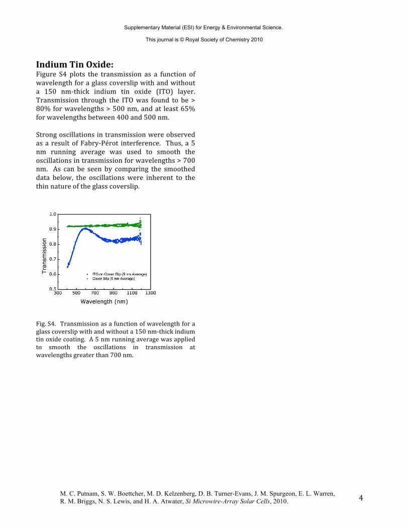
Figure S4 plots the transmission as a function ofwavelengthforaglasscoverslipwithandwithouta 150 nm‐thick indium tin oxide (ITO) layer.Transmission through the ITOwas found to be >80%forwavelengths>500nm,andat least65%forwavelengthsbetween400and500nm.Strongoscillationsintransmissionwereobservedasa resultofFabry‐Pérot interference. Thus,a5nm running average was used to smooth theoscillationsintransmissionforwavelengths>700nm. As can be seen by comparing the smootheddata below, the oscillations were inherent to thethinnatureoftheglasscoverslip.

Fig.S4. Transmissionasafunctionofwavelengthforaglasscoverslipwithandwithouta150nm‐thickindiumtinoxidecoating.A5nmrunningaveragewasappliedto smooth the oscillations in transmission atwavelengthsgreaterthan700nm.

Supplementary Material (ESI) for Energy & Environmental Science.

This journal is © Royal Society of Chemistry 2010

M. C. Putnam, S. W. Boettcher, M. D. Kelzenberg, D. B. Turner-Evans, J. M. Spurgeon, E. L. Warren, R. M. Briggs, N. S. Lewis, and H. A. Atwater, Si Microwire-Array Solar Cells, 2010. 5

Experimental:Wire Array Growth. Si microwire arrays were grown as described previously.5 The

growth substrates were boron‐doped p++‐Si (111) wafers, having a resistivity, ρ < 0.001

Ω·cm,thatwerecoatedwith450nmofthermaloxide(SiliconQuestInternational).Arrays

of4‐μm‐diametercircularholes,onasquarelatticewitha7μmpitch,weredefinedinthe

oxide by photolithographic exposure anddevelopment of a photoresist layer (Microchem

S1813), followed by a buffered HF(aq) (BHF) etch (Transene Inc.) The holes were then

filled with 600 nm of Cu (ESPI metals, 6N) via thermal evaporation onto the patterned

photoresist, followed by liftoff. Patterned substrates approximately 1.5 cm × 1.5 cm in

dimensionwerethenannealedinatubefurnacefor20minat1000°CunderH2flowingata

rate of 500 sccm. Wire growth was performed by the introduction of SiCl4 (Strem,

99.9999+%),BCl3(Matheson,0.25%inH2),andH2(Matheson,researchgrade)atflowrates

of10,1.0,and500sccm,respectively,for30min. Followinggrowth,thetubewaspurged

withN2at200sccmandwasallowedcoolto~650°Coverthecourseof~30min.

p­n JunctionFabrication. Followinggrowth theCucatalystwas removed fromthewire

arraysbyetchingin5%HF(aq)for30s,6:1:1byvolumeH2O:H2O2(30%inH2O):conc.HCl

(aq.) at 75°C for 15min, and 20wt % KOH (aq.) at 20°C for 60s. A conformal SiO2

diffusion‐barrier that was 200nm in thickness was grown via dry thermal oxidation at

1100°C for2h. Thewirearraysampleswere thencoatedwitha solution that contained

4.4g hexamethycyclotrisiloxane (Sigma‐Aldrich), 1g PDMS (Sylgard 184, Dow Corning),

and 0.10g of curing agent in 5ml of dicholoromethane; spun at 1000RPM for 30s; and

curedat150°Cfor30min,toproducea10–20μmthickPDMSlayerselectivelyatthebase

ofthewirearray.6Afteraquicketch(~2s)ina1:1mixtureof1.0Mtetrabutylammonium

fluorideintetrahydrofuran(Sigma‐Aldrich)anddimethylformamide(PDMSetch)26andaDI

rinse,thesepartiallyinfilledarrayswereimmersedfor5mininBHF,toremovetheexposed

diffusion‐barrieroxide. ThePDMSwasthencompletelyremovedbyetchingfor30minin

PDMS etch. A 10min piranha etch (3:1 aq. conc. H2SO4:H2O2)was performed to remove

residualorganiccontamination. Afteretchingthewiresfor5s in10%HF(aq), thermalP

diffusionwasperformedusingsolidsourceCeP5O14wafers(Saint‐Gobain,PH‐900PDS)at

850°Cfor10min(As‐GrownandScatterer)or15min(PRS)underanN2ambient,toyielda

Supplementary Material (ESI) for Energy & Environmental Science.

This journal is © Royal Society of Chemistry 2010

M. C. Putnam, S. W. Boettcher, M. D. Kelzenberg, D. B. Turner-Evans, J. M. Spurgeon, E. L. Warren, R. M. Briggs, N. S. Lewis, and H. A. Atwater, Si Microwire-Array Solar Cells, 2010. 6

radialp‐njunctioninthewireregionsunprotectedbythethermaloxide.A30setchinBHF

wasusedtoremovethesurfacedopantglass.

PhotovoltaicDeviceFabrication. TheAs­Growncellwasfabricatedasfollows. Afterp‐n

junctionfabrication,thewirearraywasheatedto150°Conahotplate,andmountingwax

(Quickstick135,SouthBayTech.)wasmeltedintothearray.Excesswaxwasremovedfrom

thearrayusingaglasscoverslip.ThemountingwaxwasthenetchedinanO2plasma(400

W,300mTorr)untilthewiretipsweresufficientlyexposedforelectricalcontacting(30‐90

min). After etching with BHF for 30 s, 150 nm of indium tin oxide [0.0007Ω·cm] was

sputtered(48W,3mTorr,20:0.75sccmAr:10%O2inAr)throughashadowmask,toserve

asatransparentcontacttothen‐typeshelloftheSimicrowires,therebydefiningtheareaof

themicrowiresolarcells. Contacttothep‐typecoreof theSimicrowireswasestablished

through thep+‐Si substrate by scribing aGa/In eutectic onto theback side of the growth

wafer.

Fabrication of the Scatterer cell was performed identically to that of the As‐Grown cell,

except that prior to infilling withwax, Al2O3 light‐scattering particles (0.08 µm nominal‐

diameter,SouthBayTechnology)wereaddedtothewirearray.Thewire‐arraywasplaced

face‐upinaflat‐bottomedglasscentrifugetubeand~3mlofanethanolicdispersionofthe

particles (~0.3mg/ml)were added. Centrifugation (~3000RPM) for 5minwas used to

drivetheparticlestothebaseofthewire‐array.

Fabricationof thePRS cellwasperformed identically to that for theScatterer cell, except

thatpriortotheadditionoftheAl2O3particles,ana‐SiNx:HpassivatinglayerandaAgback

reflectorwereaddedtothecell.Afterp‐njunctionfabrication,thewirearrayswereetched

for5mininBHF,tocompletelyremovetheremainingoxidediffusionbarrier. Astandard

cleanwasthenperformed(10minin5:1:1byvolumeH2O:H2O2(30%inH2O):NH4OH(15%

inH2O)at75°C,30s inBHF,10min in6:1:1byvolumeH2O:H2O2(30%inH2O):conc.HCl

(aq.)at75°C,30sinBHF),priortodepositionofana‐SiNx:Hlayer(~140nmthickatthe

wire tip and ~ 60 nm thick at the wire base) using plasma‐enhanced chemical vapor

deposition,asdescribedpreviously.1Thea‐SiNx:Hwasthenetchedfor15sinBHF,priorto

the deposition of a total of 1 µm planar‐equivalent of Ag via thermal evaporation (two

successive500nmevaporationsattwodifferentspecimen‐tiltangles(±~5degrees)with

Supplementary Material (ESI) for Energy & Environmental Science.

This journal is © Royal Society of Chemistry 2010

M. C. Putnam, S. W. Boettcher, M. D. Kelzenberg, D. B. Turner-Evans, J. M. Spurgeon, E. L. Warren, R. M. Briggs, N. S. Lewis, and H. A. Atwater, Si Microwire-Array Solar Cells, 2010. 7

sample rotation, to ensure continuous coverage of the growth substrate). The arraywas

theninfilledwith~5μmofPDMSusingaprocesssimilartotheonedescribedabove.This

PDMSetchbarrierallowedtheAgatthewiretipsandsidewallstobeselectivelyremoved

byetching for6.5min in8:1:1methanol:NH4OH(15% inH2O):30wt.%aq.H2O2. A thin

layer (~40 nm) of SiO2 was then sputtered to improve the incorporation of the Al2O3

particles. The Al2O3 scattering elements, mounting wax, and ITO were then added as

describedabove.

Characterization. Dark and light current‐voltage measurements were performed on a

probe stationwith a 4‐point source‐measure unit (Keithley 238). Contact to the ITO top

contact was made with a micromanipulator‐controlled Au‐coated tungsten probe tip.

Simulated solar illuminationwas provided by a 1000W Xe arc lampwith airmass (AM

1.5G)filters(Oriel),calibratedto1‐sunilluminationbyanNREL‐traceableSireferencecell

(PVMeasurements,Inc.).Spectralresponsemeasurementswereperformedinanoverfilled

geometryusingchopped(30Hz)illuminationfroma300WXearclampcoupledtoa0.25m

monochromator (Oriel) that provided ~2 nm spectral resolution. The specimen

photocurrentwasnormalized(byarea)tothatofa3mm‐diametercalibratedphotodiode,

to determine the external quantum yield. The signals weremeasuredwith independent

lock‐in detection of the sample and calibration channels. Scanning photocurrent

microscopymeasurementswereperformedusingaconfocalmicroscope(WiTEC)inalight‐

beam‐inducedcurrent(LBIC)configurationdescribedpreviously.9 Scanningphotocurrent

microscopy (SPCM) images were formed by rastering each device beneath a ~1.0 µm‐

diameterlaserspot(λ=650nm)whilerecordingtheshort‐circuitcurrent(0Vbias)under

otherwisedarkconditions. Multiple90µmx90µmSPCMimagesweremanuallystitched

together and post‐processed to determine the active cell area using image processing

software(ImageJ)(seeSupportingInformationFig.S3.)

Supplementary Material (ESI) for Energy & Environmental Science.

This journal is © Royal Society of Chemistry 2010


Recommended