Creation of a dual-porosity and dual-depth micromodel for the study of multiphase flow in complex porous mediaWonjin Yun, Cynthia M. Ross, Sophie Roman, and Anthony R. Kovscek*a
Energy Resources Engineering, Stanford University367 Panama Street, Stanford, CA 94305-2220
In the following sections, we provide information to supplement the article content. First, we describe the processes of spin coating, alignment for exposure, and developing of silicon wafers. Second, we provide details of the porosity, permeability calculation, and stability test for the image-sampling methodology.
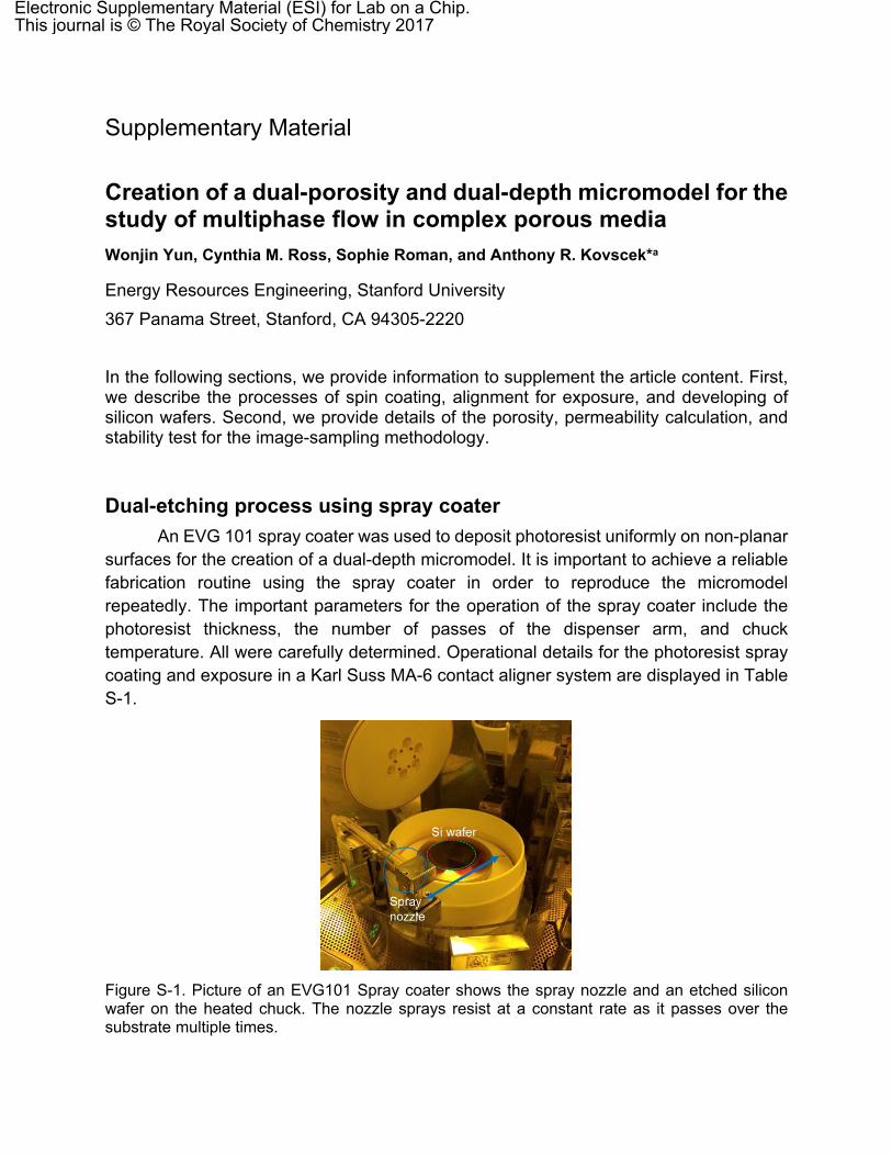
Dual-etching process using spray coater An EVG 101 spray coater was used to deposit photoresist uniformly on non-planar
surfaces for the creation of a dual-depth micromodel. It is important to achieve a reliable fabrication routine using the spray coater in order to reproduce the micromodel repeatedly. The important parameters for the operation of the spray coater include the photoresist thickness, the number of passes of the dispenser arm, and chuck temperature. All were carefully determined. Operational details for the photoresist spray coating and exposure in a Karl Suss MA-6 contact aligner system are displayed in Table S-1.
Figure S-1. Picture of an EVG101 Spray coater shows the spray nozzle and an etched silicon wafer on the heated chuck. The nozzle sprays resist at a constant rate as it passes over the substrate multiple times.
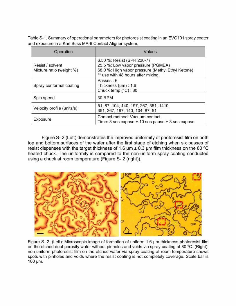
Table S-1. Summary of operational parameters for photoresist coating in an EVG101 spray coater and exposure in a Karl Suss MA-6 Contact Aligner system.
Operation Values
Resist / solventMixture ratio (weight %)
6.50 %: Resist (SPR 220-7)25.5 %: Low vapor pressure (PGMEA)68.0 %: High vapor pressure (Methyl Ethyl Ketone)** use with 48 hours after mixing.
Figure S- 2 (Left) demonstrates the improved uniformity of photoresist film on both top and bottom surfaces of the wafer after the first stage of etching when six passes of resist dispenses with the target thickness of 1.6 µm ± 0.3 µm film thickness on the 80 ºC heated chuck. The uniformity is compared to the non-uniform spray coating conducted using a chuck at room temperature (Figure S- 2 (right)).
Figure S- 2. (Left): Microscopic image of formation of uniform 1.6-µm thickness photoresist film on the etched dual-porosity wafer without pinholes and voids via spray coating at 80 ºC. (Right): non-uniform photoresist film on the etched wafer via spray coating at room temperature shows spots with pinholes and voids where the resist coating is not completely coverage. Scale bar is 100 µm.
The photoresist-coated wafer was further processed in the subsequent exposure step followed by the developing step. The wafer was exposed to the UV light at a wavelength of 365 nm and 15 mW/cm2 of intensity. An exact “complete-pore” overlay mask pattern alignment during the exposure step (f), shown in Fig. 4, is critical to expose the previously etched area in step (c) in Fig. 4 for the second etching.
Figure S-3. (Left): Stage in Karl Suss MA-6 Contact Aligner system was moved to align the pore space of the etched “partial-pore” wafer (b) with the pore space on in “complete-pore” overlay mask (a). (Right): demonstration of the successful alignment of in “complete-pore” overlay mask to the etched wafer during the exposure step in “complete-pore” dual-etching process.
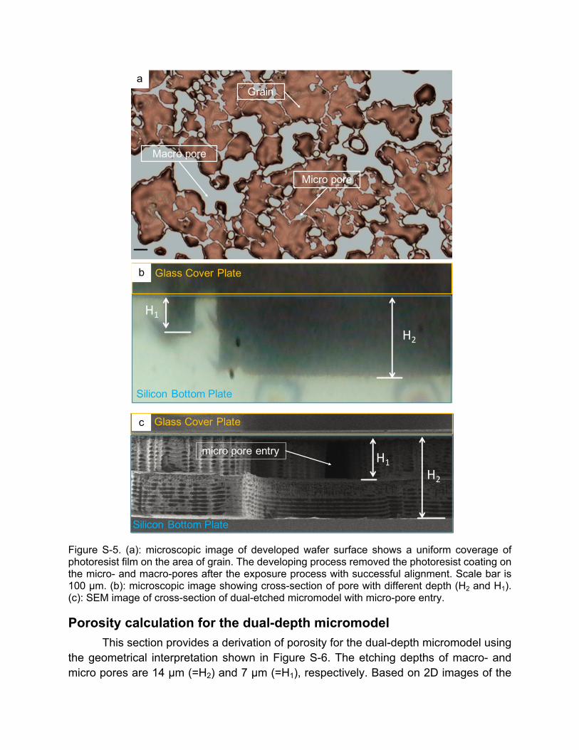
For the developing process, the automated track system was abandoned, because the dispensed developer (MF-26A) solution has poor coverage (Figure S-4, left) over the wafer surface with photoresist coating. The manual developing process consists of three cycles of soaking the exposed wafer into the developer MF-26A (2.3% TMAH, base) for 50 sec and rinsing with Deionized water (Right of Figure S-4). Figure S-5 shows the microscopic image of the removal of the photoresist in the area with UV light exposure.
Figure S-4. (Left): partially covered wafer by the developer under the dispense arm of the automated track system. (Right): manual developing process where the wafer is immersed in the developer (MF-26A) after exposure.
Grain
Macro pore
Micro pore
Glass Cover Plate
Silicon Bottom Plate
H1H2
micro pore entry
Glass Cover Plate
H1
H2
Silicon Bottom Plate
a
b
c
Figure S-5. (a): microscopic image of developed wafer surface shows a uniform coverage of photoresist film on the area of grain. The developing process removed the photoresist coating on the micro- and macro-pores after the exposure process with successful alignment. Scale bar is 100 µm. (b): microscopic image showing cross-section of pore with different depth (H2 and H1). (c): SEM image of cross-section of dual-etched micromodel with micro-pore entry.
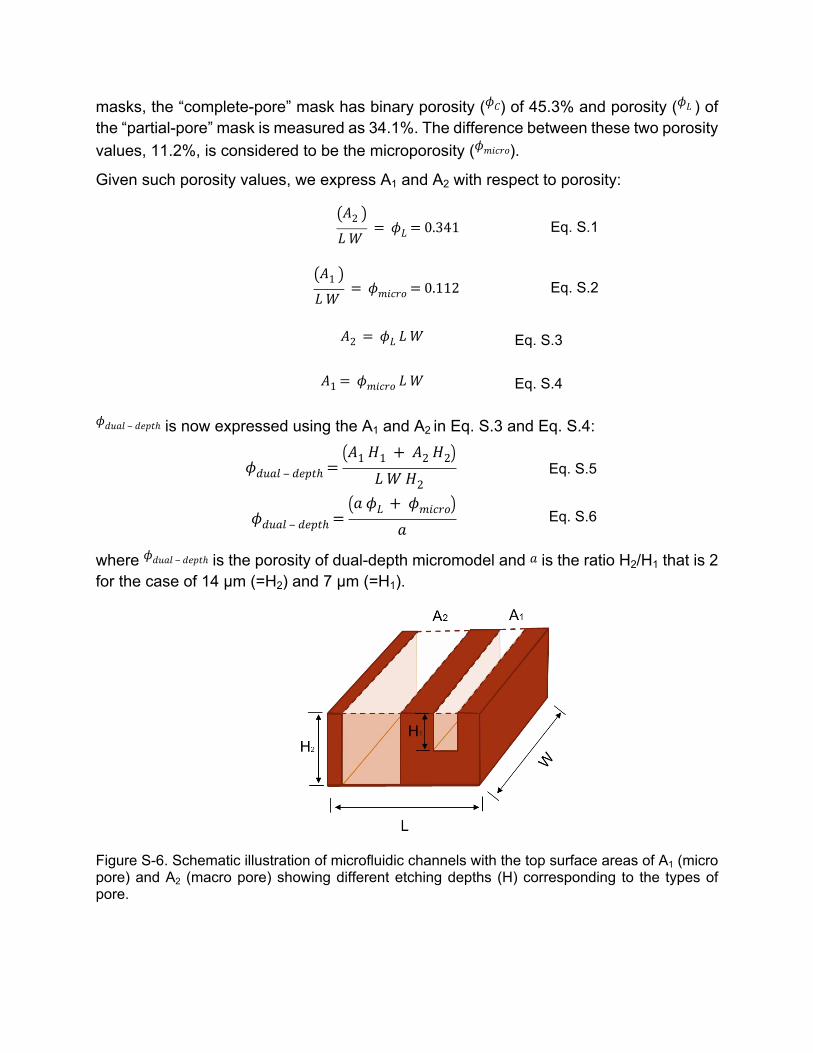
Porosity calculation for the dual-depth micromodelThis section provides a derivation of porosity for the dual-depth micromodel using
the geometrical interpretation shown in Figure S-6. The etching depths of macro- and micro pores are 14 µm (=H2) and 7 µm (=H1), respectively. Based on 2D images of the
masks, the “complete-pore” mask has binary porosity ( ) of 45.3% and porosity ( ) of 𝜙𝐶 𝜙𝐿
the “partial-pore” mask is measured as 34.1%. The difference between these two porosity values, 11.2%, is considered to be the microporosity ( ). 𝜙𝑚𝑖𝑐𝑟𝑜
Given such porosity values, we express A1 and A2 with respect to porosity:
(𝐴2 )𝐿 𝑊
= 𝜙𝐿 = 0.341 Eq. S.1
(𝐴1 )𝐿 𝑊
= 𝜙𝑚𝑖𝑐𝑟𝑜 = 0.112 Eq. S.2
𝐴2 = 𝜙𝐿 𝐿 𝑊 Eq. S.3
𝐴1 = 𝜙𝑚𝑖𝑐𝑟𝑜 𝐿 𝑊 Eq. S.4
is now expressed using the A1 and A2 in Eq. S.3 and Eq. S.4:𝜙𝑑𝑢𝑎𝑙 ‒ 𝑑𝑒𝑝𝑡ℎ
𝜙𝑑𝑢𝑎𝑙 ‒ 𝑑𝑒𝑝𝑡ℎ =
(𝐴1 𝐻1 + 𝐴2 𝐻2)𝐿 𝑊 𝐻2
Eq. S.5
𝜙𝑑𝑢𝑎𝑙 ‒ 𝑑𝑒𝑝𝑡ℎ =
(𝑎 𝜙𝐿 + 𝜙𝑚𝑖𝑐𝑟𝑜)𝑎
Eq. S.6
where is the porosity of dual-depth micromodel and is the ratio H2/H1 that is 2 𝜙𝑑𝑢𝑎𝑙 ‒ 𝑑𝑒𝑝𝑡ℎ 𝑎
for the case of 14 µm (=H2) and 7 µm (=H1).
Figure S-6. Schematic illustration of microfluidic channels with the top surface areas of A1 (micro pore) and A2 (macro pore) showing different etching depths (H) corresponding to the types of pore.
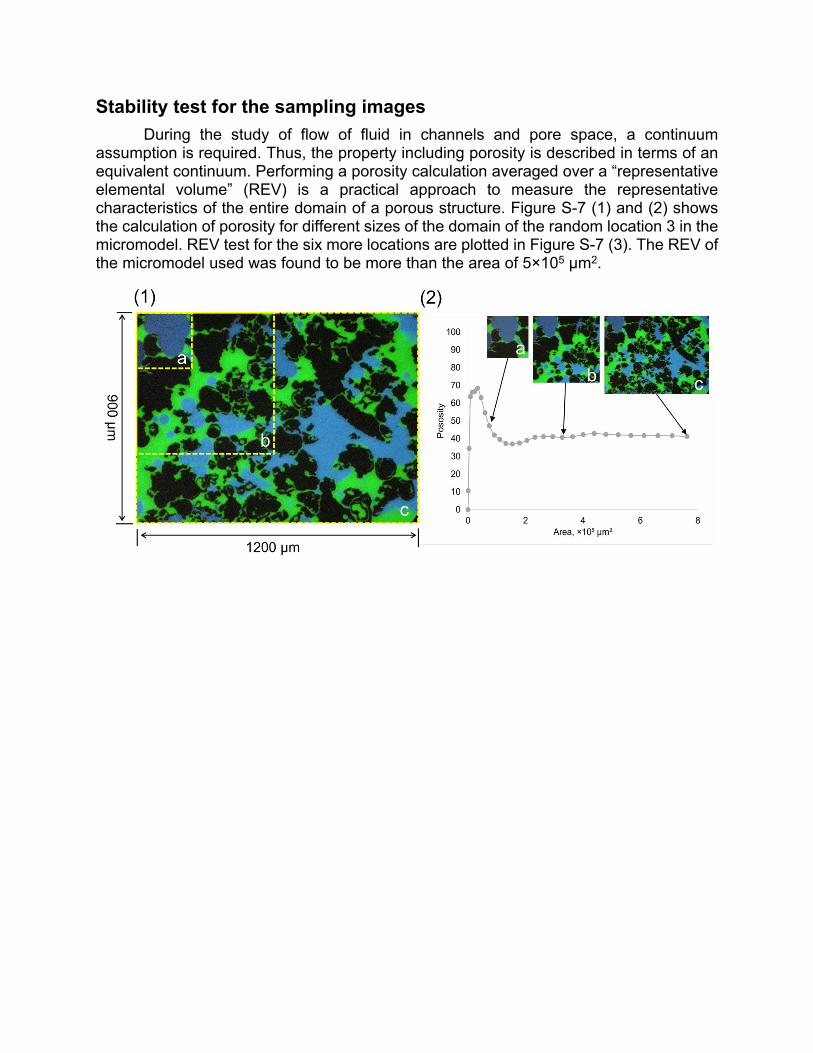
Stability test for the sampling images During the study of flow of fluid in channels and pore space, a continuum
assumption is required. Thus, the property including porosity is described in terms of an equivalent continuum. Performing a porosity calculation averaged over a “representative elemental volume” (REV) is a practical approach to measure the representative characteristics of the entire domain of a porous structure. Figure S-7 (1) and (2) shows the calculation of porosity for different sizes of the domain of the random location 3 in the micromodel. REV test for the six more locations are plotted in Figure S-7 (3). The REV of the micromodel used was found to be more than the area of 5×105 µm2.
Figure S-7. (1): Image taken at the random location 3 and total 30 different size of sub-domains (for instance, yellow-dashed rectangular areas) for porosity calculation. (2): a graph for the porosities versus the area of sub-domains in the location 3. (3): a graph for the porosities versus the area of sub-domains for all seven random locations of micromodel showing that a representative elemental volume (REV) reached around the domain size of 5×105 µm2 except for the location 5. Inset shows that the standard deviation of porosities from all seven random locations reach a plateau (~ 5%) around REV.
A stability test of the image sampling was conducted as shown in Figure S-8. In this example, the plot shows that the averaged saturation stabilizes as the number of images increases. Figure S-8 demonstrates that five images are sufficient to determine the fluid saturation. For this study, nine images were sampled from random locations within each of the nine repeating pore patterns and were used to obtain the residual water saturation (Srw) for the end-point water and oil permeability (Krw and Kro, respectively).
Figure S-8. Fluid saturations calculated by averaging saturations with an increasing number of images.
Permeability calculationA procedure to find the values for the permeability is demonstrated in Figure S-9.
After the water flooding followed by the n-decane injection at 100 psi, the end point relative permeability of oil (kro) at residual water saturations (Sw) were evaluated using the best linear fit of data points as shown in Figure S-9 (c). After the water injection at 100 psi as shown in Figure S-9 (e), the end point relative permeability of water (krw) at residual oil saturations (Sro) were evaluated.
Figure S-9. Schematic demonstrating the entire process of permeability measurement
Figure S-10. Plots to obtain the end point permeability (ko and kw) for the calculation of the end point relative permeability (kro and krw). (Top): the plot shows the data points for ko and linear fit for dual-depth (●) and single- depth (×). (Bottom): the plot shows the data points for kw and linear fit for dual-depth (●) and single- depth (×). The slopes of the fitted line for each case indicate the permeability in Darcy.