Page 1
advances.sciencemag.org/cgi/content/full/2/8/e1600418/DC1
Supplementary Materials for
Battery-free, stretchable optoelectronic systems for wireless optical
characterization of the skin
Jeonghyun Kim, Giovanni A. Salvatore, Hitoshi Araki, Antonio M. Chiarelli, Zhaoqian Xie,
Anthony Banks, Xing Sheng, Yuhao Liu, Jung Woo Lee, Kyung-In Jang, Seung Yun Heo,
Kyoungyeon Cho, Hongying Luo, Benjamin Zimmerman, Joonhee Kim, Lingqing Yan, Xue Feng,
Sheng Xu, Monica Fabiani, Gabriele Gratton, Yonggang Huang, Ungyu Paik, John A. Rogers
Published 3 August 2016, Sci. Adv. 2, e1600418 (2016)
DOI: 10.1126/sciadv.1600418
The PDF file includes:
note S1. Fabrication procedure for devices.
note S2. FEA and optimization of device layout.
fig. S1. Size and thickness of the AMS SL13A NFC chip.
fig. S2. Circuit diagram of the pulse rate monitoring device and an image of the
device mounted on the forearm.
fig. S3. Coil characterization.
fig. S4. Device functionality.
fig. S5. Inductive coupling for various operating distances between the primary
and secondary coil.
fig. S6. Temperature change during operation.
fig. S7. Current measurement of each LED during switching.
fig. S8. The distribution of maximum principal strain in the copper layer of the
deformed oximeter device.
fig. S9. Data captured wirelessly from the forearm during up-and-down arm
movement.
fig. S10. Data captured wirelessly from the forearm during deformation.
fig. S11. Wireless device benchmarked against a commercial NIR spectroscopy
system.
fig. S12. UV dosimeter with one LED.
fig. S13. Four-color spectrometer.
fig. S14. Electromagnetic properties with different media.
fig. S15. Colored PDMS measurement using the four-color spectrometer.
Page 2
fig. S16. Noise OD of the oximeter.
fig. S17. Ultimate concentration resolution of HHb and O2Hb.
table S1. Values of the components used in the device for heart rate monitoring.
table S2. Values of the components used in the oximeter.
table S3. Values of the components used in the device for the UV dosimeter.
table S4. Values of the components used in the device for the four-color
spectrometer.
Legends for movies S1 to S3
Other Supplementary Material for this manuscript includes the following:
(available at advances.sciencemag.org/cgi/content/full/2/8/e1600418/DC1)
movie S1 (.avi format). A movie of switching LEDs during the blood oximeter
device operation.
movie S2 (.avi format). A movie of switching LEDs during the four-color
spectrometer device operation.
movie S3 (.avi format). A movie of switching LEDs during the four-color
spectrometer device operation in water.
Page 3
Supplementary Materials
Here we report a detailed description of the process to fabricate and transfer the devices.
Additional pictures and measurements are also reported to complement those included in the
main text.
note S1. Fabrication procedure for devices
Sample preparation
1 Spin coat Cu foil (5 μm thick, Oak Mitsui Micro‐thin series) with polyimide (PI2545;
HD Microsystems, 3000 rpm for 30 s)
2 Anneal at 150 °C for 5 min
3 Anneal at 250 °C under vacuum for 75 min
4 Clean a glass slide (Acetone, IPA rinse)
5 Spin coat glass slide with polydimethylsiloxane (PDMS; Sylgard184, 3000 rpm for 30
s)
6 Laminate PI-coated Cu foil onto PDMS coated glass slide with PI side down
1st metal layer patterning (stretchable coil pattern)
7 Pattern photoresist (PR; AZ 4620, 3000 rpm for 30 s, anneal at 110 °C for 3 min)
through iron oxide mask with UV irradiance for 300 mJ cm-2.
8 Develop in aqueous developer (AZ400K, diluted 1:2 volume ratio, ~40 s)
9 Wet etch with Cu etchant (CE-100, Transense)
10 Remove PR with Acetone, IPA rinse
VIA hole patterning
11 Spin coat with PI (2000 rpm for 30 s)
12 Anneal at 150 °C for 5 min
13 Anneal at 250 °C under vacuum for 75 min
14 Pattern photoresist (PR; AZ 4620, 3000 rpm for 30 s, anneal at 110 °C for 3 min)
through iron oxide mask with UV irradiance for 300 mJ cm-2.
15 Develop in aqueous developer (AZ400K, diluted 1:2 volume ratio, ~40 s)
16 Etch PI (RIE; 200 mTorr, 20 sccm O2, 150 W, 900 s)
17 Remove PR with Acetone, IPA rinse
18 Remove oxide with oxide remover (Flux, Worthington)
2nd layer patterning (interconnects)
19 E-beam 1 μm Cu
Page 4
20 Pattern PR AZ4620
21 Wet etch Cu with Cu etchant
22 Remove PR with Acetone, IPA rinse
Device isolation
23 Spin coat with PI (2000 rpm for 30 s)
24 Anneal at 150 °C for 5 min
25 Anneal at 250 °C under vacuum for 75 min
26 E-beam 50 nm SiO2
27 Pattern PR AZ4620
28 Etch SiO2 (50 mTorr, 40 sccm CF4, 100 W, 10 min)
29 Etch PI (300 mTorr, 20 sccm O2, 200 W, 1800 s)
30 Clean with Acetone, IPA rinse
31 Remove oxide with oxide remover
Substrates preparation
32 Pulse-rate monitor: An ultrathin (~25 μm) medical adhesive (Acrylic adhesive,
Scapa Healthcare)
33 Blood oximeter: An ultrathin low modulus silicone elastomer (Silbione) coated black
textile substrate
34 UV dosimeter: ~300 μm of silicone elastomer (PDMS)
35 Four-color spectrometer: ~500 μm of silicone elastomer (Ecoflex)
Transfer
36 Pick up the pattern with water soluble tape
37 E-beam Ti (5 nm) / SiO2 (100 nm) on water soluble tape
38 Activate each substrate (Silicon elastomer) with UV-Ozone exposure for 3 min
39 Bond water soluble tape to PDMS with patterns facing down
40 Remove water soluble tape with water
Chip assembly
41 Remove oxide with oxide remover
42 Solder with indium/silver soldering paste (~165 oC)
43 Encapsulate with silicon elastomers
Page 5
note S2. FEA and optimization of device layout
The commercial software ABAQUS (ABAQUS Analysis User’s Manual 2010, V6.10) was
used to study mechanics of the devices and to aid in the design of optimized layouts. The
compliant substrates (PDMS and Ecoflex) were modeled by hexahedron elements (C3D8R)
while the stiff films (Cu and PI) were modeled by composite shell elements (S4R). Three
mesh densities were used to ensure the accuracy and convergence of numerical results, with
the numbers of elements to be 80000, 320000 and 1200000 for the coarse, medium, and fine
meshes, respectively. For the medium mesh, the minimal mesh size was ~0.1 of the
smallest feature dimension (e.g., minimum fillet radius). All meshes showed the same
distributions of displacement and strain while the difference in the maximum strain between
medium and fine meshes was ~1.2 %.
The positions of the chips and the widths of serpentine interconnects were optimized to
satisfy some competing requirements from mechanics and electrical designs. For example,
narrow interconnects improve the elasticity stretchability, but increase the electrical
resistance. An iterative optimization process was adopted to carefully balance these and
other mechanical and electric considerations. The position of the chip was optimized to
avoid entanglement of interconnects and contact between components.
Page 6
fig. S1. Size and thickness of the AMS SL13A NFC chip. (A) The size of the bare die is
2.38 mm x 2.38 mm. (B) The thickness of the die is ~100 μm, which is comparable to a
human hair.
fig. S2. Circuit diagram of the pulse rate monitoring device and an image of the device
mounted on the forearm. (A) The device consists of one led and one photodetector which is
reverse biased and one amplifier in trans-impedance configuration. The output signal of the
amplifier is connected to the analog input of the analog/digital converter of the NFC chip and
transmitted wirelessly to an NFC reader. (B) A picture of the device mounted on the forearm
for pulse monitoring.
Page 7
table S1. Values of the components used in the device for heart rate monitoring. The names
of the components refer to the circuit schematic of fig. S2A.
Component Value
Rf 100 kΩ
R 681 Ω
C0 1 μF
R3 2.37 kΩ
R4 23.7 kΩ
figure S3: Coil characterization. (A) Inductance and resistance of a circular coil at 13.56
MHz. (B) Inductance and resistance of a rectangular coil at 13.56 MHz.
Page 8
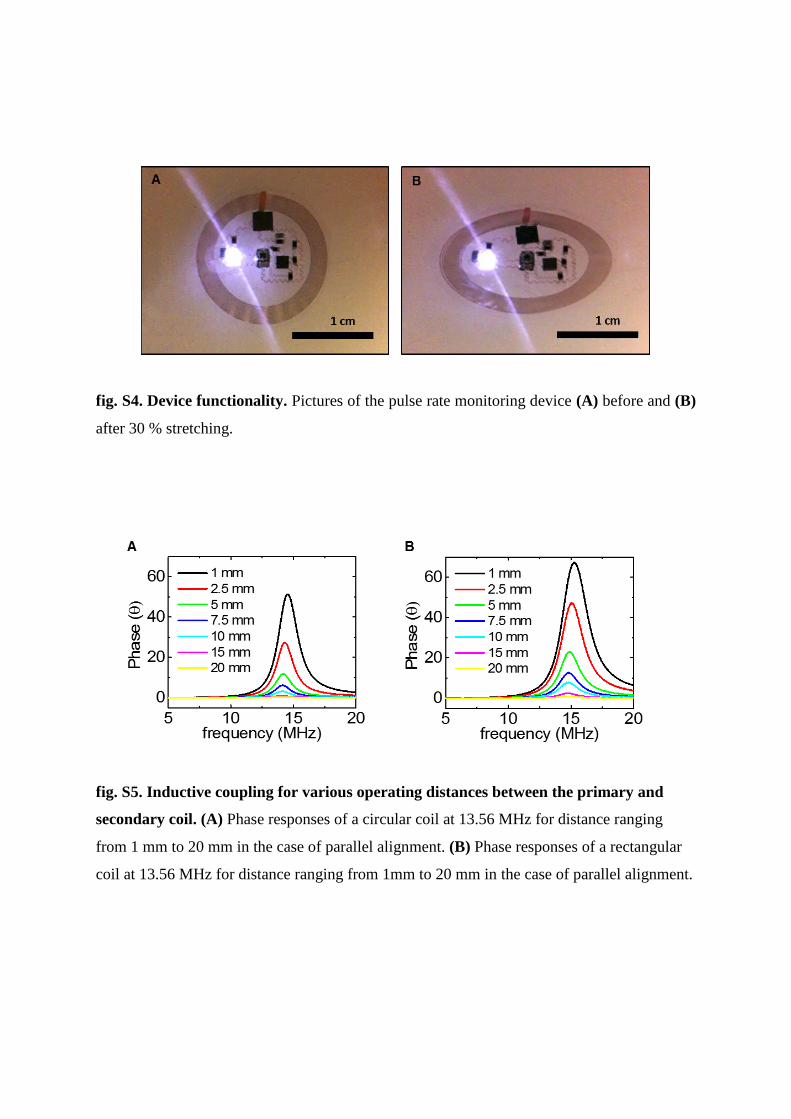
fig. S4. Device functionality. Pictures of the pulse rate monitoring device (A) before and (B)
after 30 % stretching.
fig. S5. Inductive coupling for various operating distances between the primary and
secondary coil. (A) Phase responses of a circular coil at 13.56 MHz for distance ranging
from 1 mm to 20 mm in the case of parallel alignment. (B) Phase responses of a rectangular
coil at 13.56 MHz for distance ranging from 1mm to 20 mm in the case of parallel alignment.
Page 9
fig. S6. Temperature change during operation.
table S2. Values of the components used in the oximeter. The names of the components
refer to the circuit schematic of Fig. 3B. The values for the R1C1 and R2C2 tanks are set in
such a way that the switching frequency of the LEDs is 2-3 times smaller than the maximum
sampling rate of the ADC (25Hz).
Component Value
Rf 511 kΩ
R 681 Ω
R1 19.6 kΩ
R2 28.7 kΩ
C0 10 μF
C1 4.7 μF
C2 4.7 μF
R3 2.37 kΩ
R4 23.7 kΩ
Page 10
fig. S7. Current measurement of each LED during switching for (A) the oximeter and
(B) the spectrometer.
fig. S8. The distribution of maximum principal strain in the copper layer of the
deformed oximeter device for the applied strain of 10 %, 20 %, and 30 %, respectively.
The elastic stretchability of the device is ~8.5 % for 0.3 % yield strain of copper. For 30 %
stretching, the maximum principal strain in copper is ~2.0 %, which is much lower than
fracture strain (~5 %) of the copper.
Page 11
0 10 20 30 40300
350
400
450
500
Volta
ge
(m
V)
Time (s)
up & down
arm movement
fig. S9. Data captured wirelessly from the forearm during up & down arm movement.
fig. S10. Data captured wirelessly from the forearm during deformation. (A) The raw
data. (B) The ratio of IR component/Red component.
Page 12
fig. S11. Wireless device benchmarked against a commercial NIRS system. (A) The
commercial oximeter is equipped with laser diodes (830 nm and 690 nm wavelength) which
transmit the light to the investigated surface using optical. Light is collected using a detector
fiber bundle and measured by a photomultiplier. (B) Data are acquired synchronously from
the two optical systems which are mounted on the forearm one close to the other. (C) During
the experiment, an inflating cuff is placed around the participant’s bicep, to occlude venous
blood flow. During the recording, the subject undergoes 120 s of vein occlusion with 60 s of
rest and recovery before and after the occlusion. The wireless sensor is read by an NFC
reader provided from the chip manufacturer (AMS) which is connected to a PC.
Page 13
table S3. Values of the components used in the device for the UV dosimeter. The names of
the components refer to the circuit schematic of Figure 3B. The distance between the LEDs
and the photodiode is of 1 mm against the 6 mm of the oximeter and this leads to different
values of resistors for the trans-impedance amplification and conditioning.
Component Value
Rf 100 kΩ
R 681 Ω
R1 51.1 kΩ
R2 100 kΩ
C0 10 μF
C1 4.7 μF
C2 4.7 μF
R3 2.37 kΩ
R4 23.7 kΩ
Page 14
fig. S12. UV dosimeter with one-LED. (A) Exploded-view schematic illustration of a
simplified version of the UV sensing device. (B) A picture of the device with a penny. (C) A
picture of the device with a smartphone. (inset) A picture of the device mounted on a skin.
D) The measurement of the UV sensor at varying UV exposure time.
Page 15
fig. S13. Four-color spectrometer. (A) A circuit diagram of the device, (B) illustration of
measurement data obtained using a frequency multiplexing scheme and (C) geometry of the
assembly of the LEDs and the photodetector.
Page 16
table S4. values of the components used in the device for the four color spectrometer.
The names of the components refer to the circuit schematic of fig. S13A. R11, R22, C11, C22
are the equivalent components to R1, R2, C1, C2, respectively, and refer to the components of
the second astable oscillator circuit which is not shown for simplicity in the scheme of fig.
S13A.
Component Value
Rf 100 kΩ
R 1 kΩ (for red/IR pair)
16.2 kΩ (for yellow/orange pair)
R1 147 kΩ (red LED)
R2 147 kΩ (IR LED)
R11 100 kΩ (yellow LED)
R22 100 kΩ (orange LED)
C0 10 μF
C1 20 μF
C2 30 μF
C11 10 μF
C22 20 μF
R3 14.7 kΩ
R4 121 kΩ
Page 17
fig. S14. (A) Measured phase responses of the device in the different mediums and (B)
corresponding simulation results. (C) Measured and simulated changes in resonant frequency
with different mediums. (D) Measured and simulated changes in Q factor with different
mediums
Page 18
fig. S15. Colored PDMS measurement using the four color spectrometer. (A) The
reflectance of seven different colored PDMS blocks. The vertical lines denote the wavelength
of each LED light. (B) Wireless measurement of the seven different colored PDMS blocks.
C) Calculated reflectance from measurement data of PDMS blocks with different colors.
The graph appears agreeable with the reflectance graph (A).
Page 19
fig. S16. Noise optical density of the oximeter. The ultimate resolution of the devices was
determined by performing a phantom measurement. The sensor was located on a side of a
cubic phantom (100 mm x 100 mm x 100 mm) that resembled biological tissue optical
properties. Data were acquired for 180 seconds. Noise estimation on the collected data
was performed by computing the standard deviation of the electrical data variation over time.
(A) Signal variability over the recorded period (estimated using standard deviation) was 1%
at 950 nm wavelength and 2.49 % at 620 nm wavelength, respectively. (B) FFT of the optical
density in (A).
Page 20
fig. S17. Ultimate concentration resolution of HHb and O2Hb. The variability in the molar
concentration of HHb and O2Hb can be calculated starting from the optical density and using
the Modified Lambert Beer Law. The estimated concentration variability is of ~0.050
mMol/L for both HHb and O2Hb.
Page 21
movie S1. A Movie of switching LEDs during the blood oximeter device operation.
movie S2. A Movie of switching LEDs during the four color spectrometer device
operation.
Page 22
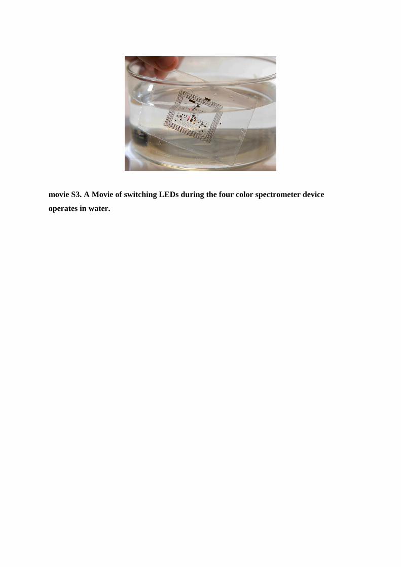
movie S3. A Movie of switching LEDs during the four color spectrometer device
operates in water.