Supplementary MaterialsSelf-assembly of Carbon Nanotubes
into Two-dimensional Geometries usingDNA Origami Templates
Hareem T. Maune Si-ping Han Robert D. Barish Marc BockrathWilliam A. Goddard III Paul W.K. Rothemund Erik Winfree
S1 Formation of and purification of NL-SWNTs
Design and formation of the linker complex. Oligos were purchased in lyophilized form from IDTDNA. Sequences are below. LNA nucleotides are written as +C+G+A, etc. All other nucleotide areDNA. Labeling domain sequences were computer-optimized (31) to minimize sequence complementar-ity, homology, and melting temperature differences with programs written in MATLAB available at:
http://www.dna.caltech.edu/DNAdesign/
Red linker main strand:5ʼ TTTTTTTTTTTTTTTTTTTTTTTTTTTTTTTTTTTTTTTTGTTGCGAGGTCTTGC+C+G+A+C+A 3ʼRed linker protection strand:5ʼ GCAAGACCTCGCAAC 3ʼBlue linker main strand:5ʼ TTTTTTTTTTTTTTTTTTTTTTTTTTTTTTTTTTTTTTTTATACGGGGCTGGTTA+G+G+A+T+G 3ʼBlue linker protection strand:5ʼ TAACCAGCCCCGTAT 3ʼ
Strands are separately dissolved in water purified by a Milli-Q unit (Millipore) to form stock so-lutions at ∼300 µM. A 2 M NaCl stock solution is created and filtered using 0.22 µm filters. Forthe red (blue) linker complex, the main strand and the protection strand are mixed with NaCl stocksolution and Milli-Q purified water to obtain 600 µL of dispersal solution with ∼ 33 µM of the mainstrand, ∼ 36 µM of the protection strand, and 0.1 M NaCl; the concentrations of the main and protectionstrands were chosen to give a 10% excess of protection strand. This solution is put in a 0.6 mL PCRtube and annealed in an Eppendorf Mastercycler from 95
C to 20C at 1
C per minute. The protectionstrand/main strand partial duplex has a melting temperature Tmelting ∼50
C in our buffers.
Dispersal of SWNTs. To create the red (blue) NL-SWNTs, ∼1 mg of dry HiPco SWNTs are addedto 400-600 µL of the dispersal solution in a 1.7 mL PCR tube. The tube is then placed in an ice-waterbath and sonicated for ∼90 minutes in a Branson 2510 sonicator (100 W). The water level inside thesonication chamber and the position of the PCR tube is adjusted to apply maximum sonication power tothe sample. The temperature of the water bath is maintained at ∼15
C. The SWNTs are sonicated untilthe solution turns a uniform gray color and all the SWNTs are completely solubilized. The solutionis then centrifuged at 16,000 g for 90 min at 15C. Following this step, the supernatant is retainedwhile the insoluble condensate is discarded. This process yields a high concentration of well-dispersedNL-SWNTs as determined by AFM and TEM images.
SUPPLEMENTARY INFORMATION doi: 10.1038/nnano.2009.311
Removal of excess linker complexes. The dispersal procedure for creating NL-SWNTs leaves a largeexcess of free linker complexes in solution that needs to be reduced before self-assembly. We apply elec-trodialysis using a Harvard Apparatus Electroprep system. A 500 µL Teflon fast dialysis tube is filledwith NL-SWNT solution and capped at both ends with 50 kD MWCO cellulose ester dialysis mem-branes. The dialysis tube is then placed in the Electroprep tank. The tank is filled with 0.1 M Na2HPO4
buffer (filtered with a 0.22 µm membrane).A constant current of 15 to 20 mA is applied across the electrodes of the Electroprep tank. The
current is run for 2 hours. The electrodes are then disconnected and the tank is washed. Fresh bufferis added, the direction of the dialysis tube is reversed such that the membrane facing the cathode nowfaces the anode, and the current is run for another two hours. Buffer exchange and current reversal arerepeated two more times before retrieving the NL-SWNT solution (8 hours total of electrodialysis).
To retrieve the NL-SWNTs, the capped dialysis tube is washed using Milli-Q purified water. It isplaced in a beaker with 0.1 M Na2HPO4 buffer and ultra-sonicated for 30 seconds to 1 minute in aBranson 2510 sonicator. This releases any NL-SWNTs stuck on the membranes back into the solutioncontained inside the dialysis tube. The tube is then uncapped and the purified NL-SWNT suspension isrecovered using an appropriate pipette.
The UV absorbance at 260 nm is measured and compared to the absorbance of an unfiltered NL-SWNT sample. We find that the self-assembly of NL-SWNTs on DNA origami is most efficient whenthe UV absorbance of the purified solution at 260 nm is < 5% of that of the initial solution. If theUV absorbance is higher, or if assembly efficiency is poor, electrodialysis is repeated with fresh filtermembranes and buffer. We usually repeat the 8 hour dialysis process three times on the same sample.Immediately after purification, NL-SWNT solutions are divided into 50 µl aliquots and stored in a -80Cfreezer where they are stable for months. Room temperature storage or 4C storage causes aggregationand decreased binding to origami after a few days; -20
C might afford stability for weeks or monthsbut we have not made a systematic study of NL-SWNT stability as a function of storage temperature.
The method we used to determine the stopping point for purification only addresses the decrease ofthe excess linker and does not address the ratio of excess free linker to linkers bound to the SWNTs,which is the more important measure since it determines whether the remaining excess of free linkersis so high that it saturates the hooks on the origami and prevents NL-SWNTS from binding to origami.Thus we used gel-electrophoresis to evaluate this ratio for some batches of NL-SWNTs.
Non-denaturing polyarylamide gel electrophoresis (ND-PAGE) is used to estimate the amount offree linker DNA. Free linkers migrate into the gel where they may be quantified, while bound linkersremain stuck on the carbon nanotubes that do not migrate from the well. We use 8% or 10% poly-acrylamide (polymerized by 1% by volume of 10% ammonium persulfate (APS) and cross-linked by0.075% by volume tetramethylethylenediamine [TEMED]) in a 1× TAE/Mg2+ buffer (40 mM Tris-acetate, 1 mM EDTA, 12.5 mM magnesium acetate, pH 8.3). A constant field of 8 V/cm is appliedacross the gel (80 V, 10 cm length, I∼34 mA, 1 mm thick mini-gel) for 3-4 hours while the buffer tem-perature is kept at 15
C. A 10 base pair ladder (Invitrogen) is used in one of the gel lanes as a lengthreference. A lane of free linker complexes is included to allow quantitation. Finally, the gel is stainedwith Sybr Gold (Invitrogen) for 25 minutes and imaged using a Bio-Rad Molecular Imager FX.
Denaturing PAGE (8%, 7 M urea, 175 V, 17.5 V/cm, 60C, stained similarly to ND-PAGE) was usedto estimate the total amount of linker DNA in the sample after the electrodialysis procedure. The idea isthat strong denaturing conditions and high temperature∗ detach the linkers from the nanotubes, so that
∗Here a field strength of 17.5 V/cm seemed to be more effective at detaching linkers than 8 V/cm. This could have beencaused incidentally by greater heating, or perhaps the somewhat elevated field played a direct role since the carbon nanotubesdo not migrate in the gel and are not free to move with the linkers.
the total can be measured. From the total and the free linker concentration, we estimate the amount oflinker bound to the carbon nanotubes (bound = total − free).
The amount of free and SWNT-bound linkers varies between different preparations of NL-SWNTs;bound linker typically ranged from ∼ 100 nM to 1 µM. As a specific example, for the batch of blueSWNTs used in Fig. 2, we estimated that the concentration of linker bound to SWNTs was 420 nMand the concentration of free linker was 120 nM, even after it had undergone a few freeze thaw cycles(and been used in successful experiments). This represents a free:bound linker ratio of ∼1:3. If theratio is too high, then presumably free linker will bind all hook sites and prevent SWNTs from binding.Because NL-SWNTs bind origami at multiple sites, some poisoning of these sites by free linker may betolerated. We have not explored the highest ratio of free:bound linker that is acceptable.
SUPPLEMENTARY INFORMATION doi: 10.1038/nnano.2009.311
S2 Design, assembly, and purification of the DNA template
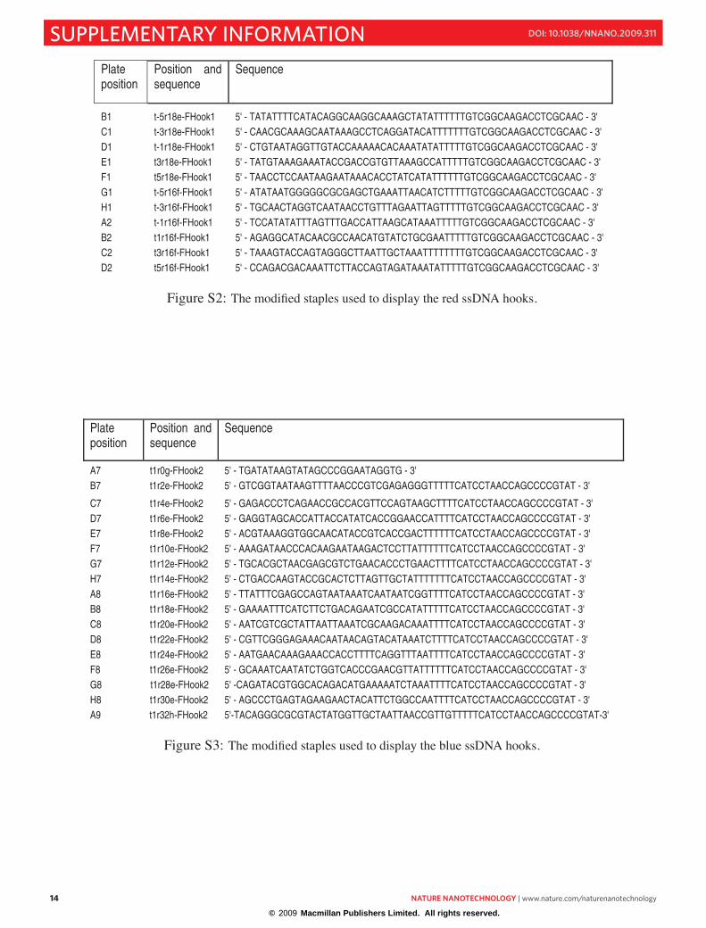
Tall rectangle origami templates. The DNA origami used in our experiments is a modified versionof the “tall rectangle” designed by Rothemund (Supplementary Information Figs. S36 and S48 in (20)).The sequences for the original origami are shown in Fig. S48 of (20). We modified the origami as shownin Fig. S1. Specifically, we replaced particular DNA staples with the strands listed in Figs. S2 and S3.Their names, listed in the “Position and sequence” columns, correspond to the names of the originalstaples shown in Rothemund’s Fig. S48 (20)but have “FHook1” or “FHook2” added. In general theirsequences differ from the original staples by the addition, on the 3’ end, of (1) a 4 thymine flexiblelinker and (2) an appropriate hook sequence.
The linker + red hook sequence is:5ʼ TTTTTGTCGGCAAGACCTCGCAAC 3ʼThis corresponds to the red linker sequence:5ʼ GTTGCGAGGTCTTGCCGACA 3ʼ
The linker + blue hook sequence is:5ʼ TTTTCATCCTAACCAGCCCCGTAT 3ʼThis corresponds to the blue linker sequence:5ʼ ATACGGGGCTGGTTAGGATG 3ʼ
The staples which are used for the blue column of hooks are actually not quite simple catenationsof original staples with the linker and blue hook sequence. The domain by which these staples bindthe origami scaffold strand is actually shifted 5 nucleotides with respect to the binding domain whichis used for the original staples—this can be observed in Fig. S1. It means that (1) the scaffold bindingdomain of each staple in the blue column is actually a composite of two staples in the same column inthe original origami, 5 nucleotides from one staple and 27 nucleotides from another and (2) one of thesequences (t1r0g-FHook2) does not actually bear a blue hook—instead it is a staple on the top edge ofthe origami that had to be modified to accomodate the shift in strand ends implied by (1).
Origami-nucleated DNA/ribbon templates. We created a larger DNA template from the DNA origamiby growing a periodic structure from the edge of the DNA origami using DNA tiles. The structures,known as zig-zag ribbons, were first described in (34) and their nucleation and growth from origami wasshown in (35). The DNA tiles constituting the ribbon are each made from four single DNA strands: twolong strands (37 nt) and two short strands (26 nt), which displaying 5-base sticky ends for binding withother tiles. A schematic for a tile attached to the origami is present at top, in Fig. S1. Tiles comprise ofjust two DNA helices and are much smaller (∼12 nm×4 nm) than a DNA origami (∼ 95 nm × 75 nm),but they can assemble into a much larger periodic ribbons, which are typically from 4-16 tiles wide andhundreds of tiles long. The long edge of the tall rectangle origami has 32 helices, so up to 16 DNAtiles can be fit onto the edge of the origami by using a set of adapter strands (35). Here we used 16-tile wide ribbons everywhere except for an experiment documented by Fig. S5d,h which used an 8-tilewide ribbon. Because the origami forms at higher temperatures than the assembly of tiles into zig-zagribbons, origami serve as good nuclei for the growth of zig-zag ribbons—a cooled mixture of theircomponent strands forms products that are almost entirely composed of DNA origami with crystallinezig-zag ribbons grown from their edge. The resulting ribbons are ∼100 nm wide and typically 500 nmto 1 µm long.
Ribbons coupled to origami are a highly visible marker for the orientation of the DNA origami (redface up or blue face up), even when imaging resolution is low. Patterns of hairpins on the DNA origamicould have served to disambiguate orientation, but experiments analysis would have been much morechallenging since they require higher resolution imaging. Qualitatively, more SWNT/DNA templatestructures were observed post-assembly when DNA origami/ribbon structures were used rather thanorigami alone; but we have not quantified this effect nor explored its mechanism. (There are manypossibilities—larger DNA nanostructures stick more strongly to mica, for example.)
DNA origami/ribbon template assembly and ligation. Short DNA strands were purchased fromIDT DNA. Single-stranded M13mp18 bacteriophage DNA, T4 DNA Polynucleotide Kinase, and T4DNA Ligase were purchased from New England Biolabs. DNA strands and buffers are mixed to obtain50 µL of the following “assembly mixture”. (Amounts of components are given as either the finalconcentration of that component, or the volume of that component added.)
1× TAE Mg2+ (12.5 mM Mg-acetate, 40 mM Tris-acetate, 1 mM EDTA, filtered with a 0.22 µm filter)1×T4 DNA ligase buffer (50 mM Tris-HCl, 10 mM MgCl2, 1 mM ATP, 10 mM Dithiothreitol)10 nM M13mp18 bacteriophage DNA50 nM of each origami staple10 nM of each DNA ribbon adapter strand100 nM of each zig-zag ribbon tile3 µL T4 Polynucleotide Kinase
The above reaction mixture is placed in a 0.6 mL PCR tube and incubated using the following tempera-ture profile:
1) 37C for 1 hour
2) 65C for 20 minutes3) 90
C for 5 minutes4) 90
C to 40C at 1
C per 1 minute5) 40
C to 25C at 1
C per 1 hour
The assembly mixture is then diluted and mixed with additional components to form 500 µL of thefollowing “ligation mixture”:
1× TAE Mg2+
1× T4 DNA ligase buffer25 µL T4 DNA ligase50 µL assembly mixture
Ligation is allowed to proceed in the above solution at room temperature for 12 to 24 hours.
Purification of DNA origami/ribbon templates. Assembled and ligated templates are separated fromother reaction products using Millipore Microcon YM-100 spin filters (100 kD MWCO). 100 µL ofthe ligation mixture is gently mixed with 300 µL of sodium-based assembly buffer (0.75 M NaCl,0.01 M Na2HPO4, pH ∼8 at 25
C, 0.22 µm filtered) and transferred to a YM-100 spin filter accordingto the product’s instructions. The filter is spun in an Eppendorf temperature-controlled centrifuge at
SUPPLEMENTARY INFORMATION doi: 10.1038/nnano.2009.311
4C and 1000 g for 12 min. 400 µL of assembly buffer is added to the retentate in the spin filter
and gently mixed using a 1000 µL pipette. The filter is spun again at 4C and 1000 g for 8 minutes.The retentate is then recovered according to the product’s instructions. The recovery should yield about100 µL of solution. (Note that the spin time for the second filtration can be adjusted to obtain approx-imately the desired volume). The recovered solution contains ∼1 nM concentration of DNA templatesin sodium buffer. We have found that without this buffer exchange, the presence of magnesium at mill-molar concentrations causes precipitation of NL-SWNTs when DNA templates are later mixed withthe NL-SWNTs. The elimination of free assembly components was verified using ND-PAGE analysis.(Origami/ribbons do not migrate in ND-PAGE gels, but excess staples which we are interested in mea-suring, do.) Ligated origami/ribbon templates remain stable in the sodium-based assembly buffer, asevidenced by subsequent AFM.
S3 Assembly of NL-SWNTs with origami-ribbon templatesWe combined NL-SWNTs with origami-ribbon templates in two different types of experiments: (1)
the binding of red NL-SWNTs or blue NL-SWNTs independently with origami-ribbon templates bear-ing cross patterns of red and blue hooks to measure the specificity of binding and fidelity of alignmentto the hooks and (2) the binding of red NL-SWNTs and blue NL-SWNTS simultaneously with origami-ribbon templates bearing cross patterns of red and blue hooks to create cross-junctions. In both cases,the basic recipe (with amounts of components given as either the final concentration of that component,or the volume of that component added) for combining NL-SWNTs with origami-ribbon templates isthe same:
∼0.75 M NaCl∼0.01 M Na2HPO4
10 µL of purified DNA templates0.5 to 3 µL of red NL-SWNTs0.5 to 3 µL of blue NL-SWNTs
This mixture (pH ∼8) is kept at 25C for 10 to 100 minutes and then deposited directly on the de-
sired substrate for characterization. We have not systematically studied the kinetics but binding timesbetween 30 and 35 minutes appear to give the best results under our conditions.
A couple comments:
1. Nanotubes probably attach to DNA templates via multiple hook-linker interactions, but the de-tails of the attachment process remain uncertain. For example, multiple linkers could first attachto multiple DNA hooks via their toeholds before each hook-linker pair completes the branch mi-gration process. Alternatively, branch migration could occur at a single attachment site followedby alignment via additional attachments. Further work is required to fully understand the attach-ment processes.
2. We do not have a direct method for quantifying the concentration of post-purification origami-ribbon templates and NL-SWNTs in the assembly solution. However, assuming every M13mp18DNA strand results in an assembled template, and every template is retained durning purifi-cation, then we would have ∼0.5 nM of origami-ribbon templates in the assembly mixture.7µm×7µm topographic fluid mode AFM scans for origami/template/NL-SWNT constructs inexperiments with a single type of tube (red or blue) typicially show 2 to 3 SWNTs for every vis-ible DNA template on the mica surface. Thus it is plausible (if binding rates of NL-SWNTs andtemplates to the mica are similar) that the concentration of NL-SWNTs could be in the low (say1-2) nanomolar range.
SUPPLEMENTARY INFORMATION doi: 10.1038/nnano.2009.311
S4 Atomic force microscopy of constructs under fluid
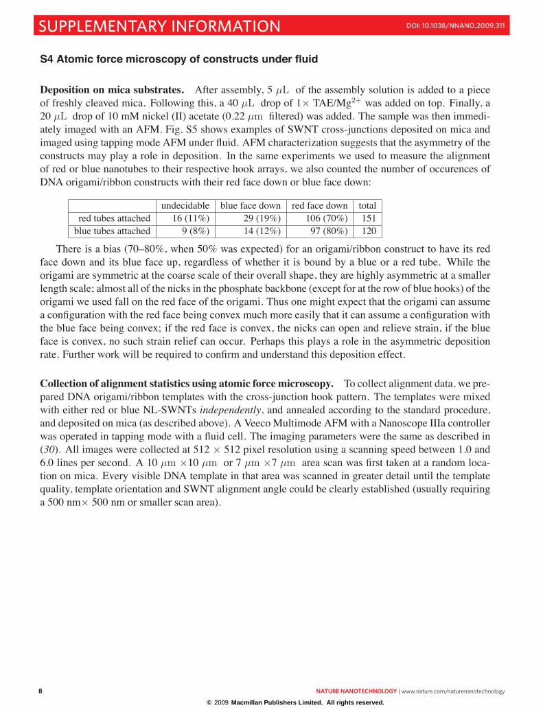
Deposition on mica substrates. After assembly, 5 µL of the assembly solution is added to a pieceof freshly cleaved mica. Following this, a 40 µL drop of 1× TAE/Mg2+ was added on top. Finally, a20 µL drop of 10 mM nickel (II) acetate (0.22 µm filtered) was added. The sample was then immedi-ately imaged with an AFM. Fig. S5 shows examples of SWNT cross-junctions deposited on mica andimaged using tapping mode AFM under fluid. AFM characterization suggests that the asymmetry of theconstructs may play a role in deposition. In the same experiments we used to measure the alignmentof red or blue nanotubes to their respective hook arrays, we also counted the number of occurences ofDNA origami/ribbon constructs with their red face down or blue face down:
undecidable blue face down red face down totalred tubes attached 16 (11%) 29 (19%) 106 (70%) 151
blue tubes attached 9 (8%) 14 (12%) 97 (80%) 120
There is a bias (70–80%, when 50% was expected) for an origami/ribbon construct to have its redface down and its blue face up, regardless of whether it is bound by a blue or a red tube. While theorigami are symmetric at the coarse scale of their overall shape, they are highly asymmetric at a smallerlength scale; almost all of the nicks in the phosphate backbone (except for at the row of blue hooks) of theorigami we used fall on the red face of the origami. Thus one might expect that the origami can assumea configuration with the red face being convex much more easily that it can assume a configuration withthe blue face being convex; if the red face is convex, the nicks can open and relieve strain, if the blueface is convex, no such strain relief can occur. Perhaps this plays a role in the asymmetric depositionrate. Further work will be required to confirm and understand this deposition effect.
Collection of alignment statistics using atomic force microscopy. To collect alignment data, we pre-pared DNA origami/ribbon templates with the cross-junction hook pattern. The templates were mixedwith either red or blue NL-SWNTs independently, and annealed according to the standard procedure,and deposited on mica (as described above). A Veeco Multimode AFMwith a Nanoscope IIIa controllerwas operated in tapping mode with a fluid cell. The imaging parameters were the same as described in(30). All images were collected at 512 × 512 pixel resolution using a scanning speed between 1.0 and6.0 lines per second. A 10 µm ×10 µm or 7 µm ×7 µm area scan was first taken at a random loca-tion on mica. Every visible DNA template in that area was scanned in greater detail until the templatequality, template orientation and SWNT alignment angle could be clearly established (usually requiringa 500 nm× 500 nm or smaller scan area).
Deposition of SWNT/DNA template constructs on SiO2 substrates. A ∼ 1 cm × 1 cm pieceof p-doped Silicon wafer with a thermally grown SiO2 layer (300 nm or 1 µm) was cleaned withdichloroethane (DCE) and isopropanol (IPA) in an ultrasonicator bath. The wafer was then exposed toO2 plasma in an Anatech SP100 plasma system (Anatech) at 80 W, 200 mTorr for 3 minutes. A 5 µL so-lution containing SWNT/DNA template constructs was then immediately deposited onto the wafer sur-face followed by a 7 µL drop of 10 mM Ni2+ acetate solution and 40 µL drop of 1× TAE/Mg2+. After1 hour of incubation at room temperature, excess salt residue was washed away using 0.1 M ammoniumacetate, (pH 6 at 25C). The wafer was dried using compressed nitrogen gas. Deposited SWNT/DNAtemplate constructs could then be imaged by tapping mode AFM on the dry silicon substrate (Fig. S6)and by scanning electron microscope (SEM) albeit with lower resolution. Although the ribbons on DNAtemplates appeared twisted and folded and under dry mode AFM, cross-junction geometry of SWNTswas typically intact (Fig. S6). Within a 400 µm2 area of the silicon wafer, we typically found 5 to 10self-assembled SWNT cross-junctions.
Lithographic fabrication of contacts to the SWNT cross-junctions. Positions of self-assembledSWNT cross-junctions are located on the Si/SiO2 substrate, with respect to the pre-fabricated referencemarkers, using an AFM. Standard electron-beam lithography techniques are employed to make elec-trical contacts to the nanotubes. Briefly, a bi-layer resist consisting of 250 nm LOR 3B lift-off resist(MicroChem, baked at 190
C for 1–3 minutes) and 150 nm PMMAC2 (MicroChem, baked at 160C for10–15 minutes) are spun on the sample. Electrode patterns are written using a Quanta 200F (FEI tools)equipped with nanometer pattern generation system (NPGS). After the development of the resist, thesample is rinsed in “DNA AWAY” (Molecular BioProducts) for 6 seconds, washed with DI water, rinsedwith HCl for 6 seconds and washed again with DI water. The rinsing steps have three purpose: first, toprime the surface (HCl has been shown to improve the hydrophilic nature of the silicates by hydrolyz-ing them, therefore, priming the metal wetting properties of the substrate surface), second, to degradesubstrate bound DNA so that it does not adversely affect the adhesion of metal electrodes to the sub-strate and third, to remove DNA from NL-SWNTs at contact regions so that it does not adversely affectthe metal-SWNT junction. (Note that at this point in the process, NL-SWNTs near the cross-junctionand DNA templates are presumably protected from the rinses by resist. However, we found that wecould not resolve the DNA templates by AFM post-liftoff.) We do not know whether the DNA onthe NL-SWNTs in the contact regions is fully degraded or whether the residue of degraded DNA iswashed away. However, NL-SWNTs treated in this manner exhibit better conductivity, presumably dueto better electrode-nanotube contact. Electrodes are then thermally evaporated via e-beam evaporator(Temescal BJD 1800). Each electrode has ∼5 nm thick Pd layer contacting the SWNT and and 40 nmAu layer protecting the Pd contact. (Palladium was chosen over gold or chromium because palladiumhas better wetting properties than gold and it has been shown to produce a smaller Schottky barrier atcontacts with SWNT than does chromium because its work function better matches that of carbon nan-otubes. Further, we chose not to apply a standard high temperature annealing protocol [e.g. 600C for30 minutes under argon] in attempt to preserve the DNA templates.) Finished devices are shown inFig. 3 and supplementary Figs. S8 and S9.
After the resist lift-off process, the device is mounted in a chip holder and electrical contact betweenthe bonding pads and holder are made using a wire bonder. The chip holder is inserted in a socketconnected to our measuring setup.
SUPPLEMENTARY INFORMATION doi: 10.1038/nnano.2009.311
In all, we attempted fabrication on 23 cross-junctions. Of these, six had measurable conductancein one or both nanotubes, three had field effect transistor (FET) like behavior. Of the three FET-likedevices, one had stable properties throughout the period of measurement.
Device characterization. All devices were characterized using similar procedures. Figs. 3 and S8show the measurement setup and results of the stable FET-like device (giving similar results over tensof measurements). Fig. S9 shows the measurement setup and results for an additional FET-like device,which was short-lived (providing just the three sweeps in Fig. 9).
Outputs from a digital-to-analog converter (DAC) card (National instruments) in a PC were usedto maintain voltages between different electrodes. Currents were measured via a current pre-amplifierwhich also served as a virtual ground. Our four-electrode setup allowed us to measure each SWNTindependently and determine its room temperature properties. In general, for a given device, we firstmeasured the two terminal current flow across each nanotube as a function of voltage (the other nanotubeis left floating) to see if good contacts had been made. Then IV curves were measured as a function ofback-gate voltage to determine if the SWNT was metallic or semiconducting (except in cases wherethe back-gate failed, as in the case of the stable device). Based on these IV curves (and if there waspotential for FET-type behavior) we chose one SWNT as the channel, and the other as the gate channel,and assigned the four electrodes as source (S), drain (D), gate (G) and auxiliary gate (g) electrodes.After picking the channel and gate nanotubes, we then measured the inter-nanotube tunneling currentas a function of applied gate voltage. Using this data, we pick a suitable range of gating voltage VG andmeasure (a) ISD at fixed VSD as a function of VG and (b) ISD at fixed VG as a function of VSD. Duringthese measurements, one terminal of the gate SWNT (G) is connected to the applied voltage while theother terminal (g) is left floating. To protect the device from the gate’s insulating layer breakdown etc.,the voltage, VG, is applied through a 100 MΩ resistor which, along with the gate capacitance, acts as alow-pass filter.
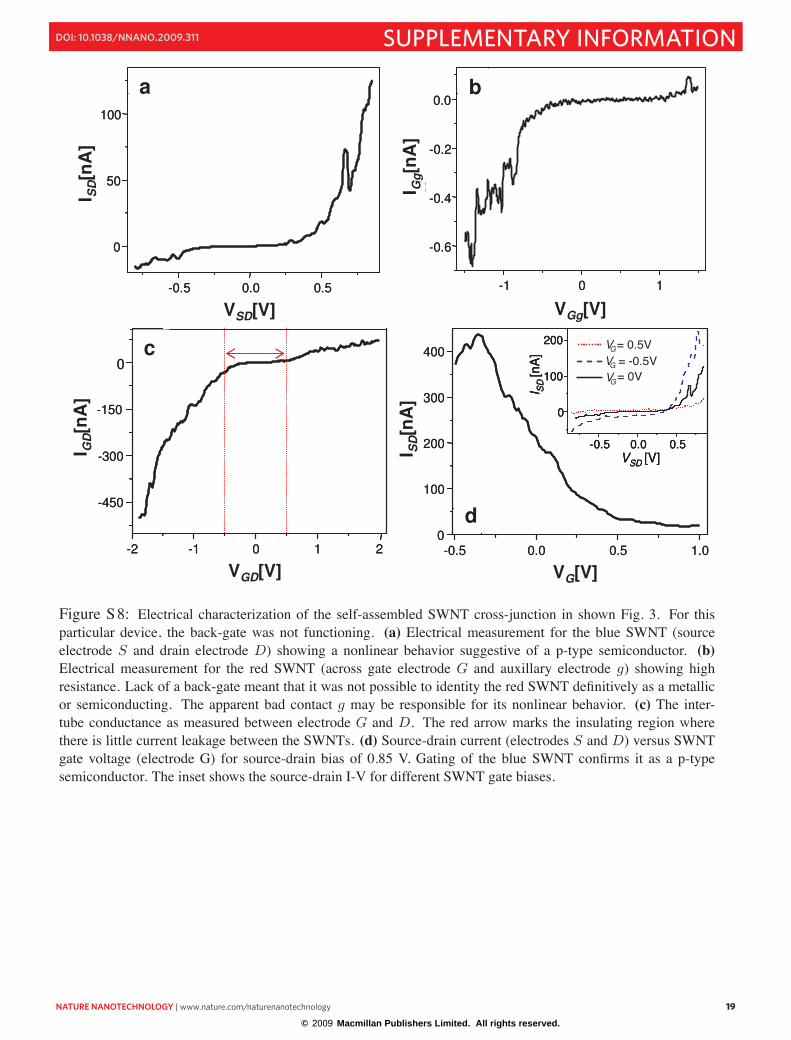
In particular, Fig. 3 shows the stable device and its function as a FET; S8 shows more detailed dataon its electronic properties. Two electrode measurements across each SWNT suggested that one SWNT(from source electrode S to drain electrode D) was a p-type semiconductor and the other SWNT (fromgate electrode G to auxillary electrode g) was either metallic or semiconducting. (For this particulardevice, the back-gate was not functioning.) We chose the SWNT across electrodes S and D to be theconducting channel due the much lower apparent resistance of that channel (∼2 MΩ, see Fig. 8). TheSWNT across electrodes G and g was chosen to be the gate channel due to that channel’s high resistance(∼6 GΩ channel resistance, see Fig. 8b). However, the inter-nanotube current measurement betweenelectrodes G and D indicates that the resistance (∼3 MΩ resistance for VGD < −0.5 V , Fig. 8c) throughthe gate nanotube and electrode G (where the gating voltage is applied) may be far lower than 1 GΩ atnegative gate voltages.
Measurement of the inter-nanotube tunneling current (Fig. S8c) also shows an insulating regionbetween VGD ∼ −0.5 V to 0.5 V. This could be due to insulation by DNA or other organic residue or aninter-nanotube Schottkey barrier. We chose to sweep VGD in this range to characterize FET-type gatingof the current channel and confirmed the identity of the blue SWNT as a p-type semiconductor.
The gate electrode G is in close proximity (∼70 nm) to the conduction channel SWNT and maycontribute to the current switching behavior shown in Fig. 8d. Further experiments are needed to under-stand the field effect gating mechanism and to decouple the contribution of the SWNT gate from that ofgate electrode.
S6 Open questions.The protocols described in this paper describe sufficient conditions for the creation of SWNT cross-
junction devices. However, there remain open questions concerning what the simplest necessary pro-cedure for creating cross-junction devices might be, as well as what parts of the protocol are mostimportant for success:
1. LNA versus DNA toeholds. We have found that, under the conditions reported above, 5 nucleotideLNA toeholds give good results. We have been unable to find conditions under which 7 and 8nucleotide DNA toeholds give good results; they resulted in cross-linking of SWNTs or aggrega-tion. For some experiments, 5 nucleotide DNA toeholds were used and SWNT-origami bindingand alignment was observed but with poor yield. However, conditions and sequences for the useof 5 nucleotide DNA toeholds were not optimized and so conditions under which less expensive,short, DNA toeholds (5 or 6 nucleotides) give good yields of cross-junctions may be found. Inaddition to its role as a stronger binding toehold, LNA may also be advantageous in this systembecause its constrained backbone may give it a lower intrinsic affinity for SWNTs; this idea hasalso not been tested.
2. Plain origami versus origami with ribbons. The use of ribbons with DNA origami appearedto increase the yield of observed structures. However we have not rigorously quantified thiseffect, and we have obtained some aligned SWNTs and cross-junctions on origami alone. Otherprotocols may be better suited for the use of DNA origami alone, for example the deposition ofDNA origami on surfaces before their assembly with SWNTs.
3. Hooks with versus hooks without poly-T segments. Yield and alignment as a function of flexibility.We added poly-T segments between staples and hooks with the idea that they would facilitateSWNT alignment by acting as joints or spacers. However, we did not test the efficacy of assemblywithout poly-T segments. This is part of a larger set of questions about the degree of alignmentas a function of hook spacing, linker length, and hook length. The effects of such variables on thequality of alignment are not understood.
4. Schemes using strand displacement versus other protected schemes without strand displacement.Here we use a protection strands to prevent the labeling domain from binding to the SWNT towhich it is attached (via the linker domain) or from cross-linking this SWNT with other SWNTs.The 5-nucleotide toehold is available for binding the hook and initiation of strand displacement.The question is whether toehold binding to the hook is itself sufficient to align a SWNT on anorigami (since multiple toeholds can bind an origami at once). Initial experiments using hooksthat are composed of only the 5 nucleotide sequence complementary to the toehold (and are thusincapable of displacing the protection strand by branch migration) indicated that binding andalignment can occur without a complete 20 nucleotide labeling domain but these experimentshave not been optimized or compared quantitatively to results with the full labeling domain. Notethat in these experiments with short hooks, the protection strand and duplex domain in the linkercomplex remain intact—thus while displacement of the protection strand may not be necessary,the rigid duplex it forms may be important in holding the toehold away from the SWNT.
5. SWNT alignment as a function of NL-SWNT purity. While preparations of NL-SWNTs with ratiosof free linker to bound linker as high as ∼1:3 gave good alignment of NL-SWNTs to origamitemplates, NL-SWNTs with a lower amount of free linker might give still better results, since free
SUPPLEMENTARY INFORMATION doi: 10.1038/nnano.2009.311
linkers presumably bind hooks on DNA origami and render them ineffective as binding sites forNL-SWNTs.
6. Why are the ends of nanotubes so often flush with the edges of DNA origami? In perhaps 25% ofcases nanotubes bind their complementary hook arrays so that one end of the nanotube is at theend of a hook array. It will be interesting to know how statistically significant this effect is, and ifit is a real effect, what is the the mechanism behind it. There are many instances where it wouldbe desirable to have nanotube ends meet rather than having nanotubes cross and so harnessing theeffect could be very useful.
7. What is the detailed structure of the linkers on the SWNT and how does this affect alignment?It is unclear what the density of the linkers are on the NL-SWNTs, whether they close packedor have gaps, whether their dispersal domains wrap the SWNTs helically or not, whether thelinkers dynamically rearrange on the SWNT surface or not, what the number of labels availablefor binding hooks is, or how any of these variables ultimately effect the alignment of SWNTs onDNA origami.
8. What is the nature of the barrier between SWNTs in our system? Can the intervening DNA layeract as a dielectric? So far, the effect of the DNA linkers and DNA origami template between car-bon nanotubes is unclear. In the device best studied, AFM showed no residual origami template atthe junction and other explanations for the observed barrier (e.g. a Schottkey barrier) are possible.However, DNA residue from the origami may have remained between the tubes, and the SWNTswere themselves coated with DNA linker complex. Lithographic steps to add metal electrodesleft visible DNA in some cases; this suggests that fabrication might be optimized to leave behindorigami templates. An important geometry to test is that of crossed carbon nanotubes bound tothe same side of the origami (which, in principle, should not be difficult to synthesize) that shouldhave less DNA between them (only the DNA linkers) and should thus exhibit a different distri-bution of device characteristics than the case with crossed carbon nanotubes on opposite sides ofthe origami. An important control will be devices that have been intentionally stripped of DNA.Improvements in locating and wiring up devices seem necessary to collect enough device data toaddress this question.
Figure S1: A schematic for the original “tall rectangle origami” (Supplementary Figs. S35 and S48 in (20)) iscompared with a schematic of the modified rectangle origami we used as a template, at right. In our new designthe leftmost column of staples was removed to decrease origami aggregation. The rightmost column of stapleswas replaced with tile adapter strands (Fig. S2 and S3) for nucleating zig-zag DNA ribbon growth. Blue dottedcircles indicate blue DNA hooks extending out of the page. Red crossed circles indicate red DNA hooks extendinginto the page.
Nanotube on top of template has greater contrast in topographic mode imaging.
Nanotube under template shows has less contrast in topographic mode AFM. Features of the DNA template are visible over the nanotube.
a
c
b
d
When SWNT is beneath the DNA template, lattice features are some times visible over the SWNT.
Details of DNA lattice visible on the template but not on the SWNT lying over the template.
Figure S4: Understanding the orientation of SWNT/origami/ribbon constructs. (a) Origami/ribbon constructshave a handedness that allows one to distinguish which face of the origami is facing up, and which is facing downon the substrate. This allows the relative orientation of a SWNT and an origami to be measured over a 180 rangerather than the 90 range possible if the origamis were used alone, without further markings. (It turns out that thealignment distributions we measure are roughly symmetric about their peak, and so in the end it would not havechanged the conclusions of the alignment data, but this might have not been the case.) (b) Another cue whichaids in understanding the structure of the cross-junctions is the topograhic height constrast of the two differentnanotubes. In general the nanotube under the template images with lower height contrast than the nanotube on topof the origami. (c) and (d) Still a third cue is the “texture” of the carbon nanotube. Nanotubes that are apparentlyon top of the origami have a smooth (yet noisy) texture do the blue nanotubes in (c) and (d). When imagedwith very high resolution, nanotubes apparently underneath the origami sometimes have a dashed or periodicappearance that seems correlated to the fine periodic structure of the origami or the ribbon, as does the red tubein (d). AFM height contrast and the texture of the nanotube are secondary cues as to the position (over or underthe origami) of the nanotubes. They are not always observed but when observed are typically consistent with theposition derived by the orientation of the origami/ribbon. Rarely they disagree—this may indicate nonspecificbinding of blue tubes to red hooks or red tubes to blue hooks, which may explain some of the few nanotubes thathave an incorrect orientation in the alignment distributions in Fig. 2.
SUPPLEMENTARY INFORMATION doi: 10.1038/nnano.2009.311
b c d
f g h
a e
Figure S5: (a)–(d) Topographic tapping mode AFM images of the self-assembled SWNT cross-junction de-posited on a mica substrate and kept under fluid. (a)–(c) show cross-junctions on origami attached to 16-widetile-wide ribbons. (d) shows a cross-junction on an origami attached to an 8-tile wide ribbon. The blue nanotubeis under the origami according to the ribbon orientation; this is consistent with the faint details of the origamifine structure that may be seen on top of it. (e)–(h) Interpretations of (a)–(d). Red and blue SWNT are indicated,origami are gray, and ribbons are green. SWNTs that apparently run origami under or ribbons have had their colordeemphasized. In (f) a ribbon that has fallen on top of part of the origami and red SWNT is represented in lightgreen. (Details of the light green ribbon can clearly be seen in the AFM coincident with the red nanotube, whichis why we interpret it as being on top of the red SWNT.)
Figure S6: (a) topographic AFM images of the self-assembled SWNT cross-junctions deposited on a siliconsubstrate. The image is taken on a dry substrate in tapping mode. The width of the ribbons is ∼100 nm. (b)interpretations of the AFM images in (a). Blue and red SWNT are indicated. Origami are indicated in gray, theribbon in dark green, and places where the ribbon folds on itself to give a double-width ribbon are in light green.Contours for DNA structures are subjective, it is difficult to tell in these images where the origami ends and theribbon begins. SWNTs that apparently run under origami or ribbons have had their color deemphasized. For thebottom cross-junction, the position of the blue and red nanotubes (over or underneath the origami), as derivedfrom the ribbon orientation and as suggested by which tube has the greater height contrast are in conflict (see S4).We have interpreted the image as though the ribbon-orientation tells the correct position, but this ribbon is sodistorted that perhaps it has been “bent up” in a way that makes its apparent handedness incorrect.
SUPPLEMENTARY INFORMATION doi: 10.1038/nnano.2009.311
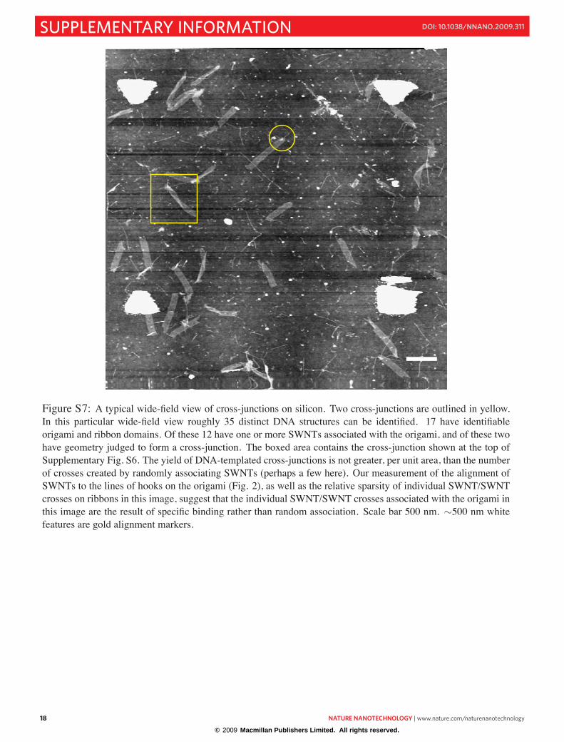
Figure S7: A typical wide-field view of cross-junctions on silicon. Two cross-junctions are outlined in yellow.In this particular wide-field view roughly 35 distinct DNA structures can be identified. 17 have identifiableorigami and ribbon domains. Of these 12 have one or more SWNTs associated with the origami, and of these twohave geometry judged to form a cross-junction. The boxed area contains the cross-junction shown at the top ofSupplementary Fig. S6. The yield of DNA-templated cross-junctions is not greater, per unit area, than the numberof crosses created by randomly associating SWNTs (perhaps a few here). Our measurement of the alignment ofSWNTs to the lines of hooks on the origami (Fig. 2), as well as the relative sparsity of individual SWNT/SWNTcrosses on ribbons in this image, suggest that the individual SWNT/SWNT crosses associated with the origami inthis image are the result of specific binding rather than random association. Scale bar 500 nm. ∼500 nm whitefeatures are gold alignment markers.
Figure S8: Electrical characterization of the self-assembled SWNT cross-junction in shown Fig. 3. For thisparticular device, the back-gate was not functioning. (a) Electrical measurement for the blue SWNT (sourceelectrode S and drain electrode D) showing a nonlinear behavior suggestive of a p-type semiconductor. (b)Electrical measurement for the red SWNT (across gate electrode G and auxillary electrode g) showing highresistance. Lack of a back-gate meant that it was not possible to identity the red SWNT definitively as a metallicor semiconducting. The apparent bad contact g may be responsible for its nonlinear behavior. (c) The inter-tube conductance as measured between electrode G and D. The red arrow marks the insulating region wherethere is little current leakage between the SWNTs. (d) Source-drain current (electrodes S and D) versus SWNTgate voltage (electrode G) for source-drain bias of 0.85 V. Gating of the blue SWNT confirms it as a p-typesemiconductor. The inset shows the source-drain I-V for different SWNT gate biases.
SUPPLEMENTARY INFORMATION doi: 10.1038/nnano.2009.311
G
D
S
250 nm
G
D
100 nm
a
b
c
d
e
-0.8 0.0 0.8
-2
0
2
4
VSD
[V]
VG
= 0 V
VG = 0.5 V
VG
= 0 V
IS
D[n
A]
f
S
Figure S9: Electrical measurement of a second SWNT cross-junction exhibiting FET-type behavior, although itwas only short-lived. (a) Dry mode AFM of the SWNT cross-junction on silicon before deposition of electrodes.(b) Interpretation of (a) showing red and blue SWNT as well as origami (gray) and ribbon (green). Orientationof the ribbon is uncertain and other cues are not present so it is impossible to tell which SWNT is on top. (c)Scanning electron micrograph (SEM) of the device after Pd/Au electrode deposition. (d) Interpretation of (c)indicating red and blue SWNTs. The DNA template is not clearly visible and may not be present after electrodefabrication. e SEM of large field showing electrodes short-lived device, alignment marks, and a variety of contactsto other devices. (f) Electrical measurement of gate-dependent switching of a resistive red SWNT, where the blueSWNT is used as the gate. A constant back gate voltage of 10 V is used for this measurement. Observed switchingbehavior was limited to just these few sweeps.