Suprconducting Transport in an LED with Nb Electrodes H. Takayanag 高柳英明 Tokyo University of Science,Tokyo International Center for Materials NanoArchitechtonics (MANA), National Institute for Materials Science, Tsukuba CREST, Japan Science and Technology Agency, Kawaguchi I. Suemune Hokkaido University R. Inoue Tokyo University of Science T. Akazaki NTT Basic Research Laboratories K. Tanaka Hamamatsu Photonics
Transcript
1
Suprconducting Transport in an LED with Nb Electrodes
H. Takayanag 高柳英明 Tokyo University of Science,Tokyo
International Center for Materials NanoArchitechtonics (MANA), National Institute for Materials Science, Tsukuba
CREST, Japan Science and Technology Agency, Kawaguchi I. Suemune Hokkaido University
R. Inoue Tokyo University of Science T. Akazaki NTT Basic Research Laboratories K. Tanaka Hamamatsu Photonics
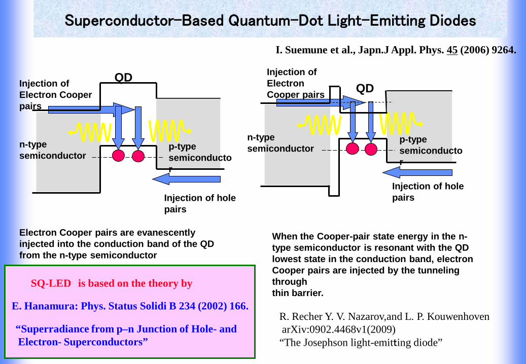
Electron Cooper pairs are evanescently injected into the conduction band of the QD from the n-type semiconductor
When the Cooper-pair state energy in the n-type semiconductor is resonant with the QD lowest state in the conduction band, electron Cooper pairs are injected by the tunneling through thin barrier.
I. Suemune et al., Japn.J Appl. Phys. 45 (2006) 9264.
E. Hanamura: Phys. Status Solidi B 234 (2002) 166.
“Superradiance from p–n Junction of Hole- and Electron- Superconductors”
SQ-LED is based on the theory by
R. Recher Y. V. Nazarov,and L. P. Kouwenhoven arXiv:0902.4468v1(2009) “The Josephson light-emitting diode”
9
Tc
Superconductor-Based Light-Emitting Diodes 1
p-InP (substrate)
p-InP (1×1017 cm-3) : 500nm
n-In0.53Ga0.47As (5×1018 cm-3) : 30nm
n-In0.7Ga0.3As (5×1018 cm-3) : 10nmNb (800 Å) Nb (800 Å)
p-InP (substrate)
p-InP (1×1017 cm-3) : 500nm
n-In0.53Ga0.47As (5×1018 cm-3) : 30nm
n-In0.7Ga0.3As (5×1018 cm-3) : 10nmNb (800 Å) Nb (800 Å)
photon
p-n junction
Y. Hayashi et al., Appl.Phys. Express 1 (’08) 011701
EL intensity enhances below Tc of Nb.
10
SiN
Au
Nb Au
Nb Nb InGaAs
110nm
B A
eV
EFn
EFp
EC
EV
Nb n-InGaAs (40 nm)
p-InP sub
Normal Holes
Electron Cooper Pairs C
11
ON (250 µA) OFF (offset bias)
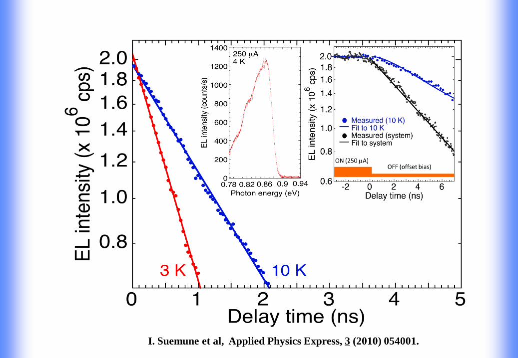
I. Suemune et al, Applied Physics Express, 3 (2010) 054001.
12
T > Tc T < Tc
Nb Nb
n-InGaAs
p-InP
Nb Nb
n-InGaAs
p-InP
Electron
Hole
Cooper pair
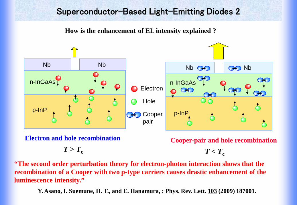
Superconductor-Based Light-Emitting Diodes 2
How is the enhancement of EL intensity explained ?
Electron and hole recombination Cooper-pair and hole recombination
Y. Asano, I. Suemune, H. T., and E. Hanamura, : Phys. Rev. Lett. 103 (2009) 187001.
“The second order perturbation theory for electron-photon interaction shows that the recombination of a Cooper with two p-type carriers causes drastic enhancement of the luminescence intensity.”
13
Superconductor-Based Light-Emitting Diodes 2
How is the enhancement of EL intensity explained ?
Y. Asano, I. Suemune, H. T., and E. Hanamura, : Phys. Rev. Lett. 103 (2009) 187001.
14
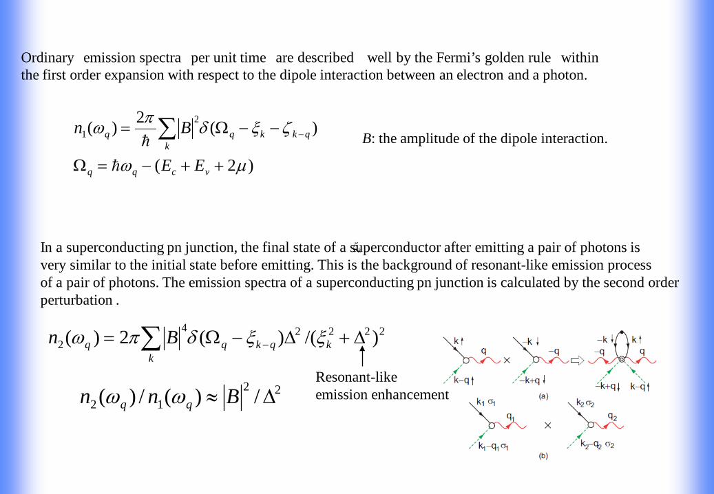
Ordinary emission spectra per unit time are described well by the Fermi’s golden rule within the first order expansion with respect to the dipole interaction between an electron and a photon.
)2(
)(2)( 21
µω
ζξδπω
++−=Ω
−−Ω= −∑vcqq
qkkqk
q
EE
Bn
B: the amplitude of the dipole interaction.
In a superconducting pn junction, the final state of a superconductor after emitting a pair of photons is very similar to the initial state before emitting. This is the background of resonant-like emission process of a pair of photons. The emission spectra of a superconducting pn junction is calculated by the second order perturbation .
222242 )/()(2)( ∆+∆−Ω= −∑ kqkq
kq Bn ξξδπω
2212 /)(/)( ∆≈ Bnn qq ωω
Resonant-like emission enhancement
kξ
15
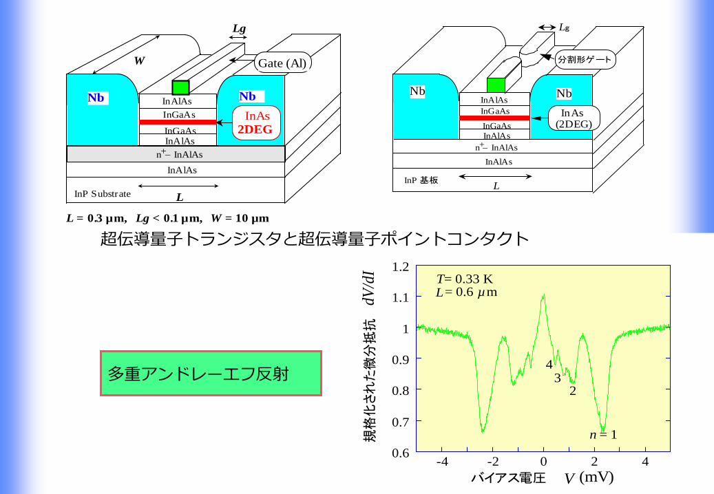
Junction Structure
Single-hetero structure (Type J)
p-InP (substrate)
p-InP (1×1017 cm-3) : 500nm
n-In0.53Ga0.47As (5×1018 cm-3) : 30nm
n-In0.7Ga0.3As (5×1018 cm-3) : 10nm
Nb (800 Å) Nb (800 Å)
Nb Nb
20 µm
20 µm
Nb slit~0.15 µm
p-InP
In order to confirm further the cooper pair effect on the recombination in the active layer, the I-V characteristics between two Nb electrodes were measured.
In0.53Ga0.47As InP
0.810 eV 1.408 eV
Positive bias
Zero bias
Depletion layer~ 10 nm
16
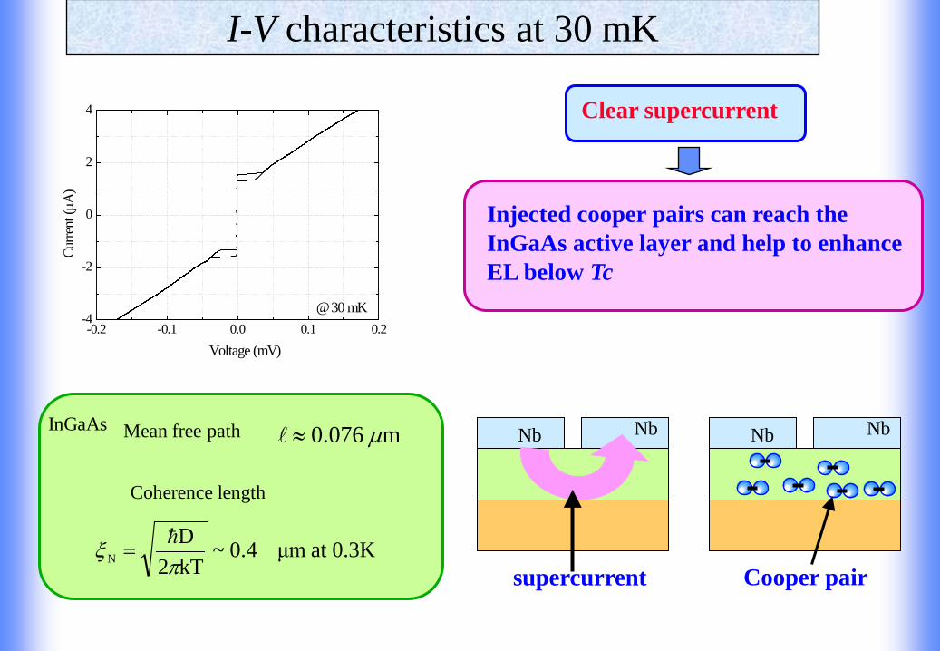
I-V characteristics at 30 mK
InGaAs Mean free path
0.3Katμm4.0~kT2D
N πξ
=
Coherence length
Clear supercurrent
Injected cooper pairs can reach the InGaAs active layer and help to enhance EL below Tc
Nb Nb Nb Nb
supercurrent Cooper pair
-0.2 -0.1 0.0 0.1 0.2-4
-2
0
2
4
Curre
nt (µ
A)
Voltage (mV)
@ 30 mK
m076.0 µ≈
17
-40 -30 -20 -10 0 10 20 30 40
0
30
60
90
120
@32 mK
Res
ista
nce
(Ohm
)
Current (µA)
-4 -3 -2 -1 0 1 2 3 40
30
60
90
120
Diff
eren
tial R
esist
ance
(Ohm
)
Voltage (mV)
@ 32 mK
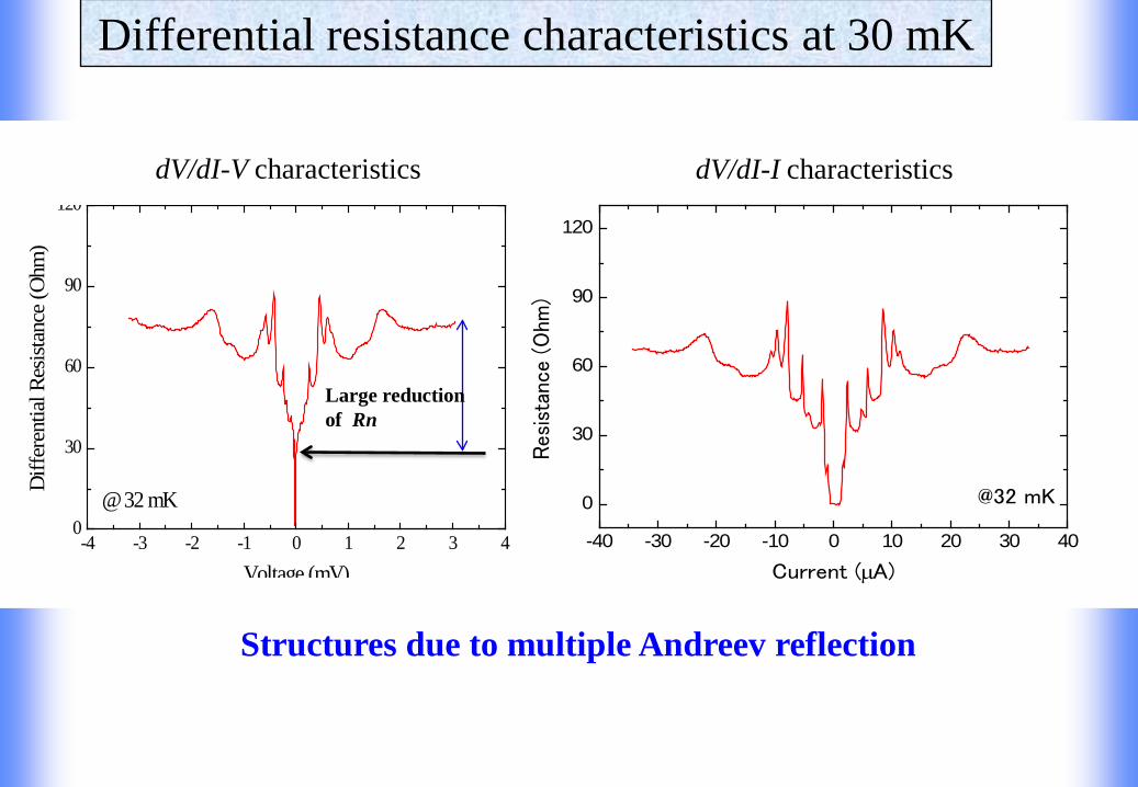
dV/dI-V characteristics dV/dI-I characteristics
Structures due to multiple Andreev reflection
Differential resistance characteristics at 30 mK
Large reduction of Rn
18
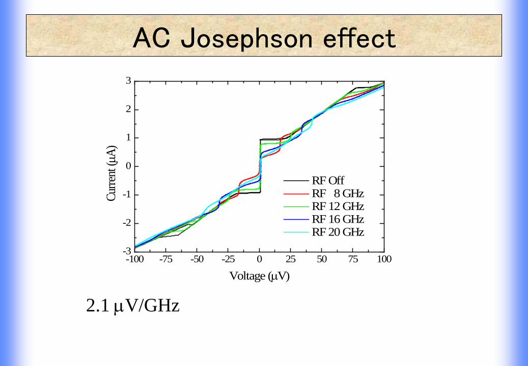
AC Josephson effect
-100 -75 -50 -25 0 25 50 75 100-3
-2
-1
0
1
2
3
RF Off RF 8 GHz RF 12 GHz RF 16 GHz RF 20 GHz
Curre
nt (µ
A)
Voltage (µV)
2.1 µV/GHz
19
pn Junction Characteristics
V, I -V, -I
Vp
A Ip
-1.0 -0.5 0.0 0.5 1.0
0
20
40
60
80
100
Injec
tion C
urren
t Ip (n
A)
Gate Voltage Vp (V)
0.0 0.2 0.4 0.6 0.8 1.00.001
0.01
0.1
1
10
100
1000
20
-6
-4
-2
0
2
4
6
Gate Voltage+1.0 V+0.8 V
+0.6 V+0.4 V
+0.2 V0 V
-0.2 V-0.4 V
-0.6 V-0.8 V
-1.0 V
Curre
nt (µ
A)
Voltage (0.1 mV/div)
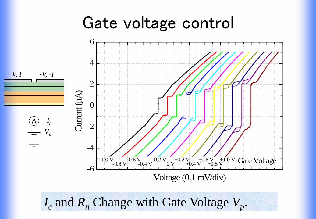
Ic and Rn Change with Gate Voltage Vp.
V, I -V, -I
Vp
A Ip
Gate voltage control
21
Gate Voltage Dependence Ic and Rn
0
25
50
75
100
125
150
-1.0 -0.5 0.0 0.5 1.00.0
0.5
1.0
1.5
2.0
2.5
Criti
cal C
urren
t Ic (µ
A)
Gate Voltage (V)
Norm
al Re
sistan
ce R
n (Ohm
)
0.001 0.01 0.1 1 10 1001.5
1.6
1.7
1.8
1.9
2.0
Criti
cal C
urren
t Ic (µ
A)
Injection Current (nA)
Ic increases by gate voltage with no Ip. IC shows saturation (or decrease) when Ip >0.
IC starts to decrease at Ip > 1nA and disappear at Ip>1 µA.
0.0 0.2 0.4 0.6 0.8 1.0 0.001
0.01
0.1
1
10
100
1000
p-n junction
Vp (V)
Ip (n
A)
22
0.001 0.01 0.1 1 10 1001.5
1.6
1.7
1.8
1.9
2.0
Criti
cal C
urren
t Ic (µ
A)
Injection Current (nA)
Three regions for gate effect on the supercurrent
Region I
Region II
Region II
Region III
III
I
Region Vp Ip Behaviour of Ic I Vp< 0.35 V Ip ~0 increases with Vp, Ip II 0.35 V < Vp< 0.88 V 0 < Ip < 10 nA constant III 0.88 V < Vp 10 nA < Ip decreases with Vp, Ip Three regions in gate voltage Vp and injection current Ip.
0
25
50
75
100
125
150
-1.0 -0.5 0.0 0.5 1.0 0.0
0.5
1.0
1.5
2.0
2.5
Crit
ical
Cur
rent
I c ( µ A
)
Gate Voltage (V)
Nor
mal
Res
ista
nce
R n (O
hm)
23
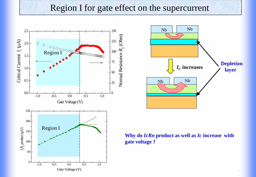
Region I
Region I for gate effect on the supercurrent
Region I
No injection current Ip = 0
Ic increases with decreasing Vp. It is because the channel for the supercurrent increases with the decrease of the depletion layer.
V, I -V, -I
Vp
A Ip
-2 V < Vp < 0.4 V
Nb Nb
Nb Nb
Depletion layer
IC increases
Cooper pairs can reach at the end of the depletion layer.
0
25
50
75
100
125
150
-1.0 -0.5 0.0 0.5 1.00.0
0.5
1.0
1.5
2.0
2.5
Criti
cal C
urre
nt I
c (µA
)
Gate Voltage (V)
Nor
mal
Res
istan
ce R
n (O
hm)
24 H. Takayanagi & T. Kawakami, Phys. Rev. Lett. 54 (1985) 2449
超伝導体
クーパー対
純2次元系に超伝導電流が流れた
巨視的波動関数をゲートポテンシャル で制御
超伝導近接効果
25
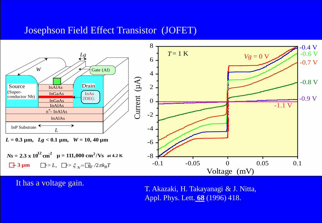
InGaAsInAlAs Source
(Super- conductor Nb)
Drain
InGaAsInAlAs
n − InAlAs
InP Substrate
+
L
InAlAs
W
InAs 2DEG
L = 0.3 µm, Lg < 0.1 µm, W = 10, 40 µm
Lg
Gate (Al)
Ns = 2.3 x 10 cm12 -2 µ = 111,000 cm /Vs2 at 4.2 K
– 3 µm >> L, >> ξ Ν = vF /2πkBT
-8
-6
-4
-2
0
2
4
6
8
-0.1 -0.05 0 0.05 0.1
Curre
nt (
µA)
Voltage (mV)
Vg = 0 V-0.4 V-0.6 V-0.7 V
-0.8 V
-0.9 V-1.1 V
T = 1 K
Josephson Field Effect Transistor (JOFET)
It has a voltage gain. T. Akazaki, H. Takayanagi & J. Nitta, Appl. Phys. Lett. 68 (1996) 418.
26
Region I
Region I for gate effect on the supercurrent
Nb Nb
Nb Nb
Depletion layer IC increases
0
25
50
75
100
125
150
-1.0 -0.5 0.0 0.5 1.00.0
0.5
1.0
1.5
2.0
2.5
Criti
cal C
urre
nt I
c (µA
)
Gate Voltage (V)
Nor
mal
Res
istan
ce R
n (O
hm)
-1.0 -0.5 0.0 0.5 1.00
50
100
150
200
250
I cR n prod
uct (
µV)
Gate Voltage (V)
Region I Why do IcRn product as well as Ic increase with gate voltage ?
27
Region III for gate effect on the supercurrent
Region III
Cp II ≥ or Cp II >>
IC goes to disappear due to non-equilibrium effect.
0
25
50
75
100
125
150
-1.0 -0.5 0.0 0.5 1.00.0
0.5
1.0
1.5
2.0
2.5
Criti
cal C
urren
t Ic (µ
A)
Gate Voltage (V)
Norm
al Re
sistan
ce R
n (Ohm
)
0.001 0.01 0.1 1 10 1001.5
1.6
1.7
1.8
1.9
2.0
Criti
cal C
urren
t Ic (µ
A)
Injection Current (nA)
Region III
III
28
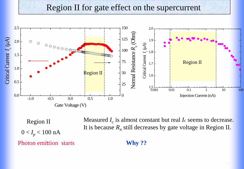
Region II for gate effect on the supercurrent
Region II Measured Ic is almost constant but real Ic seems to decrease. It is because Rn still decreases by gate voltage in Region II. 0 < Ip < 100 nA
Why ?? Photon emittion starts
0
25
50
75
100
125
150
-1.0 -0.5 0.0 0.5 1.00.0
0.5
1.0
1.5
2.0
2.5
Criti
cal C
urren
t Ic (µ
A)
Gate Voltage (V)
Norm
al Re
sistan
ce R
n (Ohm
)
0.001 0.01 0.1 1 10 1001.5
1.6
1.7
1.8
1.9
2.0
Criti
cal C
urren
t Ic (µ
A)
Injection Current (nA)
Region II
Region II
29
-1.0 -0.5 0.0 0.5 1.00
50
100
150
200
250
I cR n prod
uct (
µV)
Gate Voltage (V)-1.0 -0.5 0.0 0.5 1.0
0.0
0.5
1.0
1.5
2.0
2.5
Criti
cal C
urren
t Ic (µ
A)
Gate Voltage (V)
extrapolated
fixed IcRn
extrapolated
fixed IcRn
0.40 0.45 0.50 0.55 0.60 0.65 0.70 0.75 0.801.8
1.9
2.0
2.1
2.2
2.3
Critical
Curr
ent
Ic (µ
A)
Gate Voltage (V)
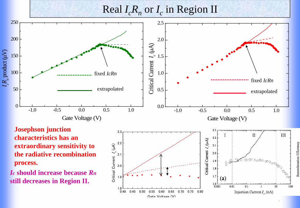
Ic should increase because Rn still decreases in Region II.
Real IcRn or Ic in Region II
Josephson junction characteristics has an extraordinary sensitivity to the radiative recombination process.
30
Nb Nb
n-InGaAs
p-InP
Cooper pair carried in the injection current Ip.
Cooper pair carried in the form of the supercurrent.
Cooper pairs carried in the form of supercurrent are destroyed by a photon emitted from the p-n junction.
31
n-InGaAs
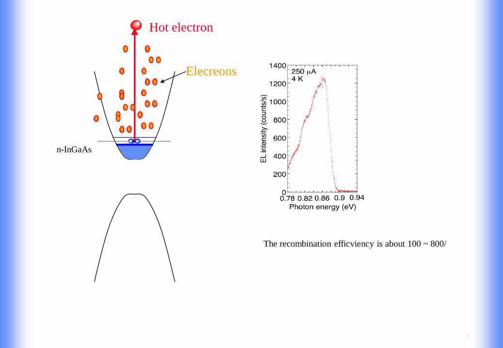
Hot electron
Elecreons
The recombination efficviency is about 100 ~ 800/
32
Measurements of a new sample
Check of the reproducibility using a new sample(80C). Cool down of both samples.
(new one 80C and old one 90C)
Heavily-filtered measurement system
Temperature dependence
Magnetic field dependence
33
New sample
-1.0 -0.5 0.0 0.5 1.0-3
-2
-1
0
1
2
3
Curre
nt (µ
A)
Voltage (mV)
30 mK, VG = 0 V
Type J P3 80C
-3 -2 -1 0 1 2 3-10
-5
0
5
10
30 mK, VG = 0 V
Curre
nt (µ
A)
Voltage (mV)
Type J P3 80C
-0.2 -0.1 0.0 0.1 0.2-4
-2
0
2
4
Curre
nt (µ
A)
Voltage (mV)
30 mK, VG = 0 V
Type J P3 90C
Ic(1) 0.6 µA … Vc 1 µV
Ic(2) 1.95 µA … Vc 100 µV
Rn 380 Ω
34
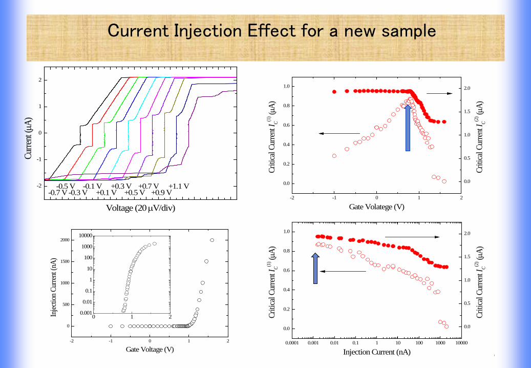
Current Injection Effect for a new sample
-2
-1
0
1
2
+1.1 V+0.9 V
+0.7 V+0.5 V
+0.3 V+0.1 V
-0.1 V-0.3 V
-0.5 V
Curre
nt (µ
A)
Voltage (20 µV/div)
-0.7 V
0 1 20.001
0.01
0.1
1
10
100
1000
10000
-2 -1 0 1 2
0
500
1000
1500
2000
Injec
tion C
urren
t (nA
)
Gate Voltage (V)
0.0
0.5
1.0
1.5
2.0
-2 -1 0 1 2
0.0
0.2
0.4
0.6
0.8
1.0
Criti
cal C
urren
t IC(1
) (µA)
Gate Volatege (V)
Criti
cal C
urren
t IC(2
) (µA)
0.0
0.5
1.0
1.5
2.0
0.0001 0.001 0.01 0.1 1 10 100 1000 10000
0.0
0.2
0.4
0.6
0.8
1.0
Criti
cal C
urren
t IC(1
) (µA)
Injection Current (nA)
Criti
cal C
urren
t IC(2
) (µA)
35
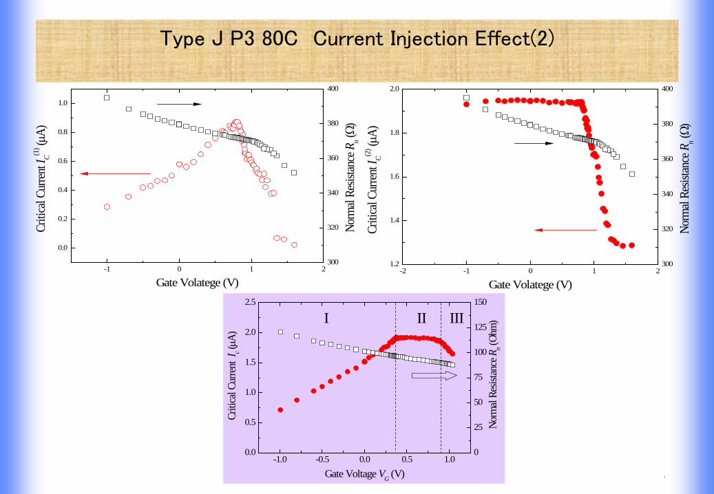
Type J P3 80C Current Injection Effect(2)
300
320
340
360
380
400
-2 -1 0 1 21.2
1.4
1.6
1.8
2.0
Criti
cal C
urren
t IC(2
) (µA)
Gate Volatege (V)
Norm
al Re
sistan
ce R
n (Ω)
300
320
340
360
380
400
-1 0 1 2
0.0
0.2
0.4
0.6
0.8
1.0
Criti
cal C
urren
t IC(1
) (µA)
Gate Volatege (V)
Norm
al Re
sistan
ce R
n (Ω)
0
25
50
75
100
125
150
-1.0 -0.5 0.0 0.5 1.00.0
0.5
1.0
1.5
2.0
2.5
Criti
cal C
urre
nt I
c (µA)
Gate Voltage VG (V)
IIIIII
Norm
al Re
sistan
ce R
n (Ohm
)
36
• Transport properties of a superconductor-based light emitting diode was measured. • A clear supercurrent was confirmed. This indicates that Cooper pairs enhance the EL below Tc. • The supercurrent (critical current Ic) showed first an enhancement and then a
saturation and finally disappear by increasing gate voltage. • The gate effects on Ic can be explained as follows. (i) Vp < 0.4 V : Ic increases due to the enhancement of the semiconductor channel. (ii) 0 < Ip <100 nA : . Ic is almost constant and Josephson current is very sensitive to radiative recombination process. Ic is almost constant. Cooper pairs might be destroyed by emitted photons. (iii) Ip > Ic : Ic disappears due to non-equilibrium effect.
Summary
37
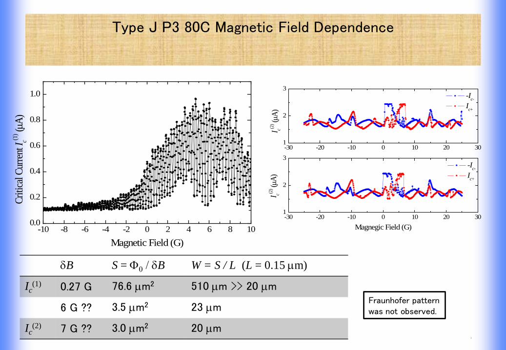
Type J P3 80C Magnetic Field Dependence
-10 -8 -6 -4 -2 0 2 4 6 8 100.0
0.2
0.4
0.6
0.8
1.0
Criti
cal C
urren
t Ic(1
) (µA)
Magnetic Field (G)
-30 -20 -10 0 10 20 301
2
3 -Ic-
Ic+
I c(2) (µ
A)
Magnegic Field (G)
-30 -20 -10 0 10 20 301
2
3 -Ic-
Ic+
I c(2) (µ
A)δB S = Φ0 / δB W = S / L (L = 0.15 µm)
Ic(1) 0.27 G 76.6 µm2 510 µm >> 20 µm
6 G ?? 3.5 µm2 23 µm
Ic(2) 7 G ?? 3.0 µm2 20 µm
Fraunhofer pattern was not observed.
38
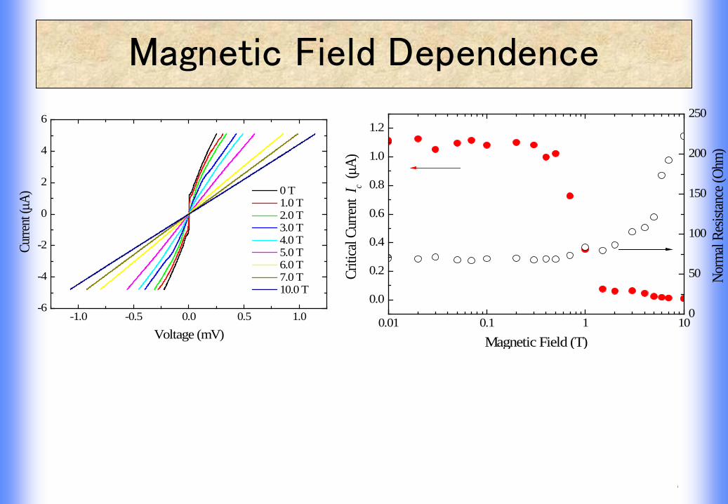
Type J P3 90C Magnetic Field Dependence (previous sample)


![SYNOPSYS™ Input General Formats · 2019. 10. 1. · format: sn option where option is one of the following: null sph rd nb rad nb cv nb ncop pcv nb [ m [ b ] ] umc nb upc nb ymc](https://static.documents.pub/doc/80x56/60b65647ea53da7a652209e1/synopsysa-input-general-formats-2019-10-1-format-sn-option-where-option.jpg)
![M36 My White LED Direct [L36-TW] selux · LED Direct Light Engine ... LED Optimized white lens MI Clear Lens w/microprism NB LMO Symmetric A2 LMO Asymmetric 20° Wall Washer BW LMO](https://static.documents.pub/doc/80x56/5acba7967f8b9a27628b8fed/m36-my-white-led-direct-l36-tw-direct-light-engine-led-optimized-white-lens.jpg)


![M36 LED Direct [L36] selux · 2021. 5. 4. · Page 1 of 14 (Rev. 05/2021) L36_SS_v2.3 ... Shielding LW LED Optimized White Lens MI Clear Lens with Microprism NB Symmetric A2 LMO ...](https://static.documents.pub/doc/80x56/612f25351ecc5158694341a7/m36-led-direct-l36-selux-2021-5-4-page-1-of-14-rev-052021-l36ssv23.jpg)

