Abstract: We have developed surface-emitting single-mode quantumcascade lasers which employ high-contrast photonic-crystal resonators. Thedevices operate on band-edge states of the photonic band-structure. Themode profile and polarization characteristics of the band-edge modes arecalculated by three-dimensional finite-difference time-domain simulation.Experimentally, the spectral properties, the far-field patterns, and thepolarization characteristics of the lasers are determined and comparedwith simulations. The good agreement between the simulations and theexperiments confirms that the hexapolar mode at the Γ-point band-edgegives rise to lasing. By using a novel and advanced fabrication method,deep and vertical PhC holes are fabricated with no metal redeposition onthe sidewalls, which improves the laser performance with respect to thecurrent status. The angular of the output beam is ≈ 15◦, and the side modesuppression ratio of the single mode emission is about 25 dB. The thresholdcurrent density at 78K and the maximum operation temperature are 7.6kA/cm2 and 220 K, respectively. The performance is mainly limited by theloss induced by surface plasmon waveguide, which can be overcome byusing an optimized dielectric waveguide structure.
References and links1. R. Colombelli, K. Srinivasan, M. Troccoli, O. Painter, C. Gmachl, F. Capasso, D. M. Tennant, A. M. Sergent,
D. L. Sivco, , and A. Y. Cho, “Quantum Cascade Photonic-Crystal Surface-Emitting Laser,” Science 302, 1374(2003).
2. K. Srinivasan, O. Painter, R. Colombelli, C. Gmachl, D. M. Tennant, A. M. Sergent, D. L. Sivco, A. Y. Cho,M. Troccoli, and C. F, “Lasing mode pattern of a quantum cascade photonic crystal surface-emitting microcavitylaser,” Appl. Phys. Lett. 84, 4164–4166 (2004).
3. Hua Zhang, L. Andrea Dunbar, Giacomo Scalari, Romuald Houdr, and Jrme Faist, ”Terahertz photonic crystalquantum cascade lasers,” Opt. Express 15, 16818-16827 (2007)
4. A. Benz, C. Deutsch, G. Fasching, K. Unterrainer, A. Andrews, P. Klang, W. Schrenk, and G. Strasser, “Activephotonic crystal terahertz laser,” Opt. Express 17, 941–946 (2009).
#126141 - $15.00 USD Received 29 Mar 2010; revised 3 May 2010; accepted 3 May 2010; published 21 May 2010(C) 2010 OSA 24 May 2010 / Vol. 18, No. 11 / OPTICS EXPRESS 11979
5. Y. Chassagneux, R. Colombelli, W. Maineult, S. Barbieri, H. E. Beere, D. A. Ritchie, S. P. Khanna, E. H. Linfield,and G. A. Davies, “Electrically pumped photonic crystal terahertz lasers controlled by boundary conditions,”Nature 457, 174 (2009).
6. G. Xu, V. Moreau, Y. Chassagneux, A. Bousseksou, R. Colombelli, G. Patriarche, G. Beaudoin, and I. Sagnes,“Surface emitting quantum cascade lasers with metallic photonic-crystal resonators,” Appl. Phys. Lett. 94,221101 (2009).
7. Y. Chassagneux, R. Colombelli, W. Maineult, S. Barbieri, S. Khanna, E. Linfield, and A. Davies, “Graded pho-tonic crystal THz quantum cascade lasers,” Appl. Phys. Lett. 96, 031104 (2010).
8. Y. Chassagneux, R. Colombelli, W. Maineult, S. Barbieri, S. Khanna, E. Linfield, and A. Davies, “Predictablesurface emission patterns in terahertz photonic-crystal quantum cascade lasers,” Opt. Express 17, 9491–9052(2009).
9. G. Xu, Y. Chassagneux, R. Colombelli, G. Beaudoin, and I. Sagnes, “Polarized single-lobed surface emission inmid-infrared, photonic-crystal, quantum-cascade lasers,” Opt. Lett. 35, 859 (2010).
10. K. Unterrainer, R. Colombelli, C. Gmachl, F. Capasso, H. Y. Hwang, A. M. Sergent, D. L. Sivco, and A. Y. Cho,“Quantum cascade lasers with double metal-semiconductor waveguide resonators,” Appl. Phys. Lett. 80(17),3060–3062 (2002).
11. S. Kohen, B. Williams, and Q. Hu, “Electromagnetic modeling of terahertz quantum cascade laser waveguidesand resonators,” J. Appl. Phys. 97, 053106 (2005).
12. O. Painter, R. Lee, A. Scherer, A. Yariv, J. O’Brien, P. Dapkus, and I. Kim, “Two-dimensional photonic band-gapdefect mode laser,” Science 284, 1819-1821 (1999).
13. M. Bahriz, V. Moreau, J. Palomo, R. Colombelli, D. Austin, J. Cockburn, L. Wilson, A. Krysa, and J. Roberts,“Room-temperature operation of λ = 7.5 µm surface-plasmon quantum cascade lasers,” Appl. Phys. Lett. 88,181103 (2006).
14. B. D’Urso, O. Painter, J. O’Brien, T. Tombrello, A. Scherer, and A. Yariv, “Modal reflectivity in finite-depthtwo-dimensional photonic-crystal microcavitites,” J. Opt. Soc. Am. B 15(3), 1155–1159 (1998).
15. The finite elements solver Comsol Multiphysics has been employed for the simulations. Bloch-periodic boundaryconditions where implemented .
16. M. Imada, A. Chutinan, S. Noda, and M. Mochizuki, “Multidirectionally distributed feedback photonic crystallasers,” Phys. Rev. B 65(19), 195306 (2002).
17. A. Bousseksou, V. Moreau, R. Colombelli, C. Sirtori, G. Patriarche, O. Mauguin, L. Largeau, G. Beaudoin,and I. Sagnes, “Surface-plasmon distributed-feedback mid-infrared quantum cascade lasers based on hybridplasmon/air-guided modes,” IEEE Electron. Lett. 44, 807 (2008).
18. K.-H. Lee, S. Guilet, G. Patriarche, I. Sagnes, and A. Talneau, “Smooth sidewall in InP-based photonic crystalmembrane etched by N2-based inductive coupled plasma,” J. Vac. S. Tech. B 26, 1326–1333 (2008).
19. G. Vecchi, F. Raineri, I. Sagnes, A. Yacomotti, P. Monnier, T. Karle, K.-H. Lee, R. Braive, L. L. Gratiet, S. Guilet,G. Beaudoin, A. Talneau, S. Bouchoule, A. Levenson, and R. Raj, “Continuous-wave operation of photonic band-edge laser near 1.55 m on silicon wafer,” Opt. Express 15, 7551–7556 (2008).
20. A. Farjadpour, D. Roundy, A. Rodriguez, M. Ibanescu, P. Bermel, J. D. Joannopoulos, S. G. Johnson, and G. Burr,“Improving accuracy by subpixel smoothing in FDTD,” Opt. Lett. 31, 2972–2974 (2006).
21. S. G. Johnson, S. Fan, P. R. Villeneuve, J. D. Joannopoulos, and L. A. Kolodziejaki, “Guided modes in photoniccrystal slabs,” Phys. Rev. B 60(8), 5751–5758 (1999).
22. S. H. Kim, S. K. Kim, and Y. H. Lee, “Vertical beaming of a wavelength-scale photonic crystal resonator,” Phys.Rev. B 73, 235117 (2006).
23. J. Vuckovic, M. Loncar, H. Mabuchi, and A. Scherer, “Optimization of the Q factor in photonic crystal Micro-cavities,” IEEE J. Quantum Electron. 38, 850 (2002).
24. H. Y. Ryu, M. Notomi, and Y. H. Lee, “Finite-difference time-domain investigation of band-edge resonant modesin finite-size two-dimensional photonic crystal slab,” Phys. Rev. B 68, 045209 (2003).
25. L. Sapienza, A. Vasanelli, R. Colombelli, C. Ciuti, Y. Chassagneux, C. Manquest, U. Genner, and C. Sirtori,“Electrically Injected Cavity Polaritons,” Phys. Rev. Lett. 100, 136806 (2008).
26. A. Bousseksou, R. Colombelli, A. Babuty, Y. De Wilde, Y. Chassagneux, C. Sirtori, G. Patriarche, G. Beaudoin,and I. Sagnes, “A semiconductor laser device for the generation of surface-plasmons upon electrical injection,”Opt. Express 17, 9391 (2009).
1. Introduction
Photonic-crystal (PhC) quantum cascade (QC) lasers merge photonic and electronic band struc-ture engineering. In particular, the use of a PhC resonator yields surface-emission - with possi-bly reduced divergence - and simultaneously spectrally single-mode behavior. Both these char-acteristics can be of interest for fundamental and application-driven reasons [1–9]. To date, PhCQC lasers have been demonstrated both in the mid-infrared and in the THz spectral ranges, but
#126141 - $15.00 USD Received 29 Mar 2010; revised 3 May 2010; accepted 3 May 2010; published 21 May 2010(C) 2010 OSA 24 May 2010 / Vol. 18, No. 11 / OPTICS EXPRESS 11980
only in the so-called band-edge configuration where the device operates on band-edge states ofthe photonic band structure [1, 5–9]. These states - typically located at high-symmetry pointsin the band structure - exhibit a high photonic density of states (and correspondingly reducedgroup velocity) as a result of the two-dimensional distributed feedback of the photonic lattice.
Various implementations for PhC QC lasers have been proposed. The first surface-emittingPhC QC laser was demonstrated by Colombelli et al. in the mid-IR [1]. Deep and vertical airholes were ICP (inductively coupled plasma) etched into the semiconductor laser layers in orderto obtain the necessary index contrast (3.4 vs 1 in this case), and reduce the device dimensions.A similar approach was employed in the THz by Zhang et al. [3] and Benz et al. [4], wherea photonic structure made of deep etched micro-pillars provides at the same time gain andin-plane optical confinement. In both cases the vertical mode confinement relied on metal-metal waveguides [10, 11], and the lasers operate in an edge-emitting configuration. Recentlyhowever, we have demonstrated a novel approach: a metallic photonic crystal, consisting ofair holes in a thin metallic layer, is directly written on the top device metallization and nosemiconductor etch is needed [5, 6]. The operation of the PhC in this case can be understoodin an intuitive way: the electromagnetic field distributions of the guided mode when the topmetallization is present or absent are very different. This large modal mismatch plays the samerole as the index contrast in standard PhCs, thus giving rise to optical feedback and eventuallyto lasing. This method has been used successfully in both the THz and mid-infrared spectralranges [6, 8]. Most importantly, judicious design of the PhC resonator permits to preciselyengineer the far-field emission pattern, the divergence angle and the polarization characteristicsof the laser [7, 9].
In order to fabricate more compact PhC QC lasers, or even PhC devices which operate ona defect mode [12], achieving an elevated index contrast is crucial. This is particularly true inthe mid-IR, where the sole patterning of the metal - though efficient - cannot induce a highindex contrast. In this work, we improve the method originally employed by Colombelli etal. [1]. A strategy for PhC fabrication is proposed which improves both the device yield andthe laser performance with respect to Ref. [1]. Besides obtaining surface laser emission witha very low divergence angle, we provide a systematic experimental and theoretical study ofthe device photonic band structure, as well as their far-field and polarization characteristics.Excellent agreement is obtained between theory and experiment.
The paper is organized as follows. In Sec. II the design of the PhC-QCLs is described:the photonic-band structure and the electromagnetic field distribution of the band-edge modesare presented. Section III focuses on material growth and device fabrication. Section IV con-tains the experimentally measured spectral properties below threshold. Section V discusses thedevice characteristics in the lasing-regime, including the light-current-voltage features, tem-perature behavior, the far-field patterns, and the polarization characteristics. In Sec. VI, three-dimensional (3D) finite-difference time-domain (FDTD) simulations are performed which pro-vide the lasing mode identification. Section VII contains the conclusion.
2. Design
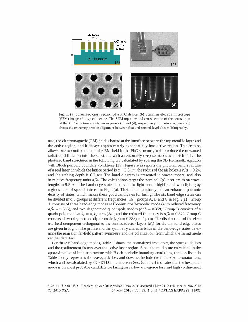
Figure 1(a) shows the schematic structure of a typical PhC-QCL studied in this work. A surface-plasmon waveguide is employed for vertical confinement [13], i.e. the QC laser active regionis sandwiched between an InP substrate and directly top metallization layers, instead of top di-electric claddings. The top metallic film acts simultaneously as surface plasmon carrying layer,and as contact layer for electric current injection. The air holes which constitute the triangularPhC lattice are ICP etched through the semiconductor active region and deep into the substrate.Although the surface plasmon waveguide will induce relatively large ohmic losses in the mid-IRrange, it is crucial for the operation of our PhC device. In a surface plasmon waveguide struc-
#126141 - $15.00 USD Received 29 Mar 2010; revised 3 May 2010; accepted 3 May 2010; published 21 May 2010(C) 2010 OSA 24 May 2010 / Vol. 18, No. 11 / OPTICS EXPRESS 11981
Fig. 1. (a) Schematic cross section of a PhC device. (b) Scanning electron microscope(SEM) image of a typical device. The SEM top view and cross-section of the central partof the PhC structure are shown in panels (c) and (d), respectively. In particular, panel (c)shows the extremey precise alignment between first and second level ebeam lithography.
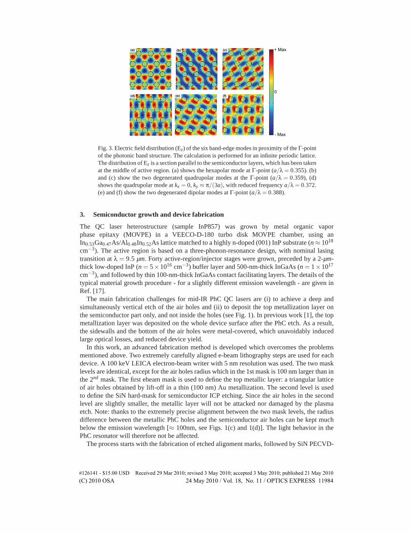
ture, the electromagnetic (EM) field is bound at the interface between the top metallic layer andthe active region, and it decays approximately exponentially into active region. This feature,allows one to confine most of the EM field in the PhC structure, and to reduce the unwantedradiation diffraction into the substrate, with a reasonably deep semiconductor etch [14]. Thephotonic band structures in the following are calculated by solving the 3D Helmholtz equationwith Bloch periodic boundary conditions [15]. Figure 2(a) reports the photonic band structureof a real laser, in which the lattice period is a = 3.6 µm, the radius of the air holes is r/a = 0.24,and the etching depth is 6.2 µm. The band diagram is presented in wavenumbers, and alsoin relative frequency units a/λ. The calculations target the nominal QC laser emission wave-lengths ≈ 9.5 µm. The band-edge states modes in the light cone - highlighted with light grayregions - are of special interest in Fig. 2(a). Their flat dispersion yields an enhanced photonicdensity of states, which makes them good candidates for lasing. The six band edge states canbe divided into 3 groups at different frequencies [16] [groups A, B and C in Fig. 2(a)]. GroupA consists of three band-edge modes at Γ-point: one hexapolar mode (with reduced frequencya/λ = 0.355), and two degenerated quadrupole modes (a/λ = 0.359). Group B consists of aquadrupole mode at kx = 0, ky ≈ π/(3a), and the reduced frequency is a/λ = 0.372. Group Cconsists of two degenerated dipole mode (a/λ = 0.388) at Γ point. The distributions of the elec-tric field component orthogonal to the semiconductor layers (Ez) for the six band-edge statesare given in Fig. 3. The profile and the symmetry characteristics of the band-edge states deter-mine the emission far-field pattern symmetry and the polarization, from which the lasing modecan be identified.
For these 6 band-edge modes, Table 1 shows the normalized frequency, the waveguide lossand the confinement factors over the active laser region. Since the modes are calculated in theapproximation of infinite structure with Bloch-periodic boundary conditions, the loss listed inTable 1 only represents the waveguide loss and does not include the finite-size resonator loss,which will be calculated by 3D FDTD simulations in Sec. 6. Table 1 indicates that the hexapolarmode is the most probable candidate for lasing for its low waveguide loss and high confinement
#126141 - $15.00 USD Received 29 Mar 2010; revised 3 May 2010; accepted 3 May 2010; published 21 May 2010(C) 2010 OSA 24 May 2010 / Vol. 18, No. 11 / OPTICS EXPRESS 11982
0.25
0.30
0.35
0.40
0.45
0.50
700
800
900
1000
1100
1200
1300
Wav
enum
ber (
cm-1)
Freq
uenc
y (a
/)
JX
(a) (b)0.0 0.5 1.0
700
800
900
1000
1100
1200
1300
Wav
enum
ber (
cm-1
)
Intensity (a.u.)
AB
C
Fig. 2. (a) Calculated photonic band structure of the PhC. The y-axis in absolute frequencyunits refers to a structure with active region thickness 3.5 µm, etching depth 6.2 µm, latticeperiod a = 3.6 µm, radius of the air holes r/a = 0.24. The light gray regions correspondto the light cone. The dark gray horizontal bands highlight the three groups of band-edgemodes relevant for lasing. (b) EL spectrum (red curve) measured under threshold at a tem-perature of 300K. The blue curve is the lasing spectrum of the same device, measured abovethreshold and at the maximum operation temperature (220K). The intensity is normalized.The absolute frequency scales are identical since the laser structure parameters are the sameas those used in the calculation of the photonic band structure.
Table 1. Normalized frequency, waveguide loss and confinement factors of the band-edgemodes calculated for an infinite PhC structure. All the modes except the one marked by ”*”are at the Γ point of the photonic-band structure. The mode marked by ”*” is at kx = 0, ky
= π/(3a).
Mode Normalized frequency Waveguide loss Confinement factor
(a/λ) (cm−1)
Hexapole 0.355 28.8 0.96
Quadrupole 0.359 33.6 0.93
Quadrupole 0.359 33.2 0.93
Quadrupole∗ 0.372 42.0 0.91
Dipole 0.388 52.2 0.80
Dipole 0.388 55.2 0.80
factor. However, the difference in waveguide loss and confinement factor between the hexapolarand the two quadrupolar modes at the Γ-point are small. As a consequence, in order to identifythe lasing mode, it is necessary to take into account the cavity loss and compare the calculatedfar-field pattern and polarization characteristics of different modes with the measured results.
#126141 - $15.00 USD Received 29 Mar 2010; revised 3 May 2010; accepted 3 May 2010; published 21 May 2010(C) 2010 OSA 24 May 2010 / Vol. 18, No. 11 / OPTICS EXPRESS 11983
(e) (f)
(a) (b) (c)
(d)
- Max
+ Max
0
Fig. 3. Electric field distribution (Ez) of the six band-edge modes in proximity of the Γ-pointof the photonic band structure. The calculation is performed for an infinite periodic lattice.The distribution of Ez is a section parallel to the semiconductor layers, which has been takenat the middle of active region. (a) shows the hexapolar mode at Γ-point (a/λ = 0.355). (b)and (c) show the two degenerated quadrupolar modes at the Γ-point (a/λ = 0.359), (d)shows the quadrupolar mode at kx = 0, ky ≈ π/(3a), with reduced frequency a/λ = 0.372.(e) and (f) show the two degenerated dipolar modes at Γ-point (a/λ = 0.388).
3. Semiconductor growth and device fabrication
The QC laser heterostructure (sample InP857) was grown by metal organic vaporphase epitaxy (MOVPE) in a VEECO-D-180 turbo disk MOVPE chamber, using anIn0.53Ga0.47As/Al0.48In0.52As lattice matched to a highly n-doped (001) InP substrate (n ≈ 1018
cm−3). The active region is based on a three-phonon-resonance design, with nominal lasingtransition at λ = 9.5 µm. Forty active-region/injector stages were grown, preceded by a 2-µm-thick low-doped InP (n = 5×1016 cm−3) buffer layer and 500-nm-thick InGaAs (n = 1×10¹⁷
cm−3), and followed by thin 100-nm-thick InGaAs contact facilitating layers. The details of thetypical material growth procedure - for a slightly different emission wavelength - are given inRef. [17].
The main fabrication challenges for mid-IR PhC QC lasers are (i) to achieve a deep andsimultaneously vertical etch of the air holes and (ii) to deposit the top metallization layer onthe semiconductor part only, and not inside the holes (see Fig. 1). In previous work [1], the topmetallization layer was deposited on the whole device surface after the PhC etch. As a result,the sidewalls and the bottom of the air holes were metal-covered, which unavoidably inducedlarge optical losses, and reduced device yield.
In this work, an advanced fabrication method is developed which overcomes the problemsmentioned above. Two extremely carefully aligned e-beam lithography steps are used for eachdevice. A 100 keV LEICA electron-beam writer with 5 nm resolution was used. The two masklevels are identical, except for the air holes radius which in the 1st mask is 100 nm larger than inthe 2nd mask. The first ebeam mask is used to define the top metallic layer: a triangular latticeof air holes obtained by lift-off in a thin (100 nm) Au metallization. The second level is usedto define the SiN hard-mask for semiconductor ICP etching. Since the air holes in the secondlevel are slightly smaller, the metallic layer will not be attacked nor damaged by the plasmaetch. Note: thanks to the extremely precise alignment between the two mask levels, the radiusdifference between the metallic PhC holes and the semiconductor air holes can be kept muchbelow the emission wavelength [≈ 100nm, see Figs. 1(c) and 1(d)]. The light behavior in thePhC resonator will therefore not be affected.
The process starts with the fabrication of etched alignment marks, followed by SiN PECVD-
#126141 - $15.00 USD Received 29 Mar 2010; revised 3 May 2010; accepted 3 May 2010; published 21 May 2010(C) 2010 OSA 24 May 2010 / Vol. 18, No. 11 / OPTICS EXPRESS 11984
deposition (200 nm) for electric current isolation. The passivation layer is then opened byreactive-ion-etching (RIE) at the PhC device sites. After realization of the contact pads (lift-off of 30nm/300nm Ti/Au), the metallic PhC is defined by e-beam lithography followed bylift-off of a 100-nm-thick Au layer. A 1.5-µ m-thick SiN layer was then deposited: it acts as thehard mask layer for the semiconductor ICP etch. The second PhC pattern is then aligned andgenerated by e-beam lithography, transferred into the SiN layer by RIE, and finally transferredinto the semiconductor layers by ICP etch up to a depth of 6.2 µm [Figs. 1(b) and 1(d)] [18]. TheSiN hard mask is finally removed and back-contact deposition (Ti/Au) concludes the process.
A series of PhC-QC lasers were fabricated, with photonic lattice periods in the 3.0− to−3.8µm range and r/a value fixed at 0.24 [Fig. 1(c)]. The dimension of the PhC structure, definedas the diameter of a circle circumscribing the hexagonal PhC device, is 150 µm. Figure 1(b)shows the scanning electron microscope image of a typical device; its central part is presentedin Fig. 1(c). Figure 1(d) shows the cross-section of the PhC structure, demonstrating deep andvertical air holes.
4. Spectral properties below laser threshold
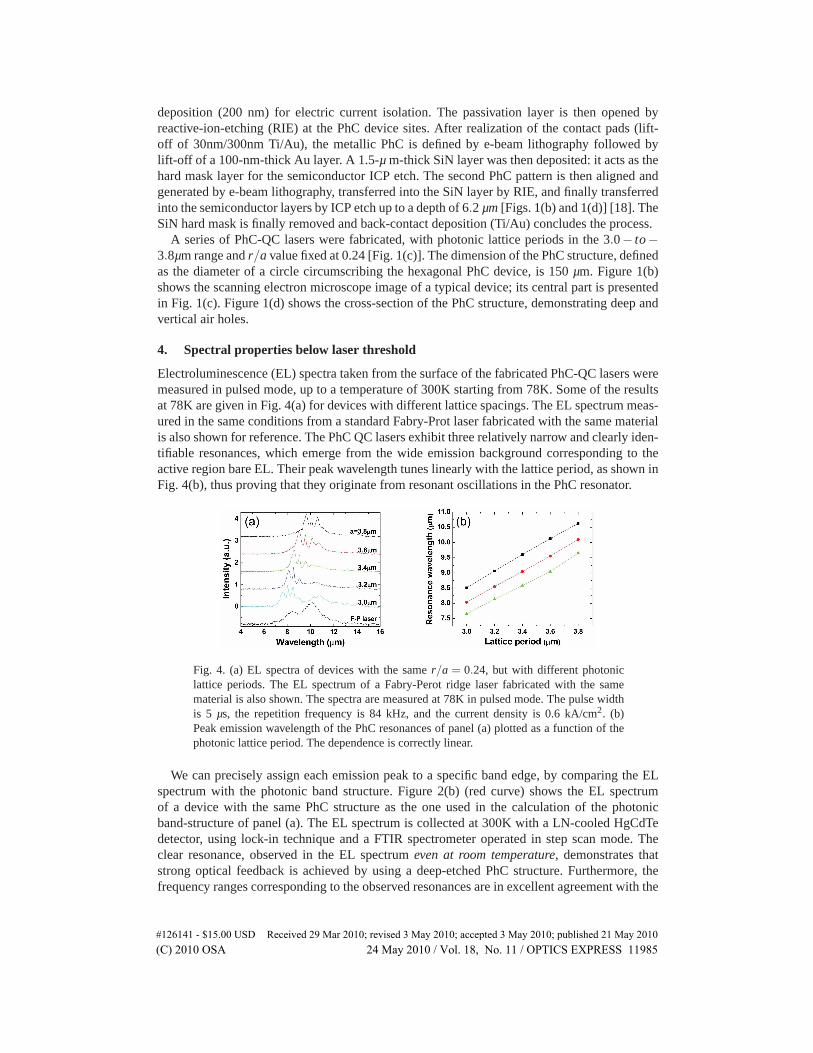
Electroluminescence (EL) spectra taken from the surface of the fabricated PhC-QC lasers weremeasured in pulsed mode, up to a temperature of 300K starting from 78K. Some of the resultsat 78K are given in Fig. 4(a) for devices with different lattice spacings. The EL spectrum meas-ured in the same conditions from a standard Fabry-Prot laser fabricated with the same materialis also shown for reference. The PhC QC lasers exhibit three relatively narrow and clearly iden-tifiable resonances, which emerge from the wide emission background corresponding to theactive region bare EL. Their peak wavelength tunes linearly with the lattice period, as shown inFig. 4(b), thus proving that they originate from resonant oscillations in the PhC resonator.
Fig. 4. (a) EL spectra of devices with the same r/a = 0.24, but with different photoniclattice periods. The EL spectrum of a Fabry-Perot ridge laser fabricated with the samematerial is also shown. The spectra are measured at 78K in pulsed mode. The pulse widthis 5 µs, the repetition frequency is 84 kHz, and the current density is 0.6 kA/cm2. (b)Peak emission wavelength of the PhC resonances of panel (a) plotted as a function of thephotonic lattice period. The dependence is correctly linear.
We can precisely assign each emission peak to a specific band edge, by comparing the ELspectrum with the photonic band structure. Figure 2(b) (red curve) shows the EL spectrumof a device with the same PhC structure as the one used in the calculation of the photonicband-structure of panel (a). The EL spectrum is collected at 300K with a LN-cooled HgCdTedetector, using lock-in technique and a FTIR spectrometer operated in step scan mode. Theclear resonance, observed in the EL spectrum even at room temperature, demonstrates thatstrong optical feedback is achieved by using a deep-etched PhC structure. Furthermore, thefrequency ranges corresponding to the observed resonances are in excellent agreement with the
#126141 - $15.00 USD Received 29 Mar 2010; revised 3 May 2010; accepted 3 May 2010; published 21 May 2010(C) 2010 OSA 24 May 2010 / Vol. 18, No. 11 / OPTICS EXPRESS 11985
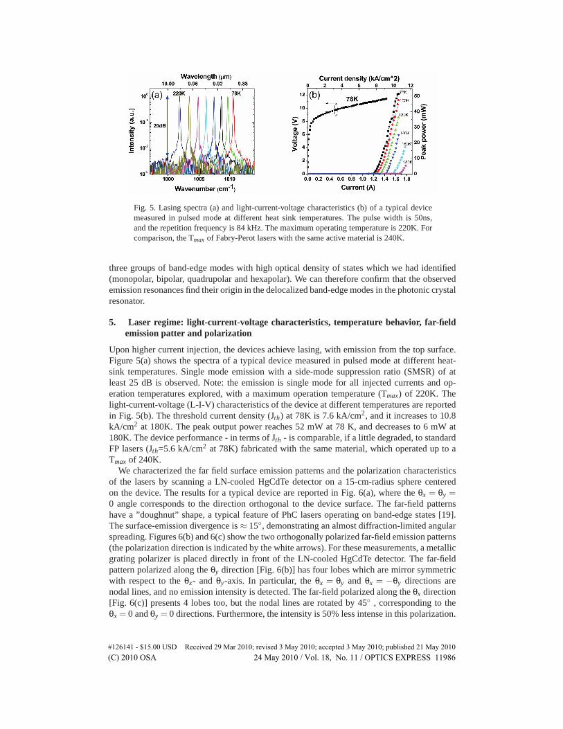
Fig. 5. Lasing spectra (a) and light-current-voltage characteristics (b) of a typical devicemeasured in pulsed mode at different heat sink temperatures. The pulse width is 50ns,and the repetition frequency is 84 kHz. The maximum operating temperature is 220K. Forcomparison, the Tmax of Fabry-Perot lasers with the same active material is 240K.
three groups of band-edge modes with high optical density of states which we had identified(monopolar, bipolar, quadrupolar and hexapolar). We can therefore confirm that the observedemission resonances find their origin in the delocalized band-edge modes in the photonic crystalresonator.
5. Laser regime: light-current-voltage characteristics, temperature behavior, far-fieldemission patter and polarization
Upon higher current injection, the devices achieve lasing, with emission from the top surface.Figure 5(a) shows the spectra of a typical device measured in pulsed mode at different heat-sink temperatures. Single mode emission with a side-mode suppression ratio (SMSR) of atleast 25 dB is observed. Note: the emission is single mode for all injected currents and op-eration temperatures explored, with a maximum operation temperature (Tmax) of 220K. Thelight-current-voltage (L-I-V) characteristics of the device at different temperatures are reportedin Fig. 5(b). The threshold current density (Jth) at 78K is 7.6 kA/cm2, and it increases to 10.8kA/cm2 at 180K. The peak output power reaches 52 mW at 78 K, and decreases to 6 mW at180K. The device performance - in terms of Jth - is comparable, if a little degraded, to standardFP lasers (Jth=5.6 kA/cm2 at 78K) fabricated with the same material, which operated up to aTmax of 240K.
We characterized the far field surface emission patterns and the polarization characteristicsof the lasers by scanning a LN-cooled HgCdTe detector on a 15-cm-radius sphere centeredon the device. The results for a typical device are reported in Fig. 6(a), where the θx = θy =0 angle corresponds to the direction orthogonal to the device surface. The far-field patternshave a ”doughnut” shape, a typical feature of PhC lasers operating on band-edge states [19].The surface-emission divergence is ≈ 15◦, demonstrating an almost diffraction-limited angularspreading. Figures 6(b) and 6(c) show the two orthogonally polarized far-field emission patterns(the polarization direction is indicated by the white arrows). For these measurements, a metallicgrating polarizer is placed directly in front of the LN-cooled HgCdTe detector. The far-fieldpattern polarized along the θy direction [Fig. 6(b)] has four lobes which are mirror symmetricwith respect to the θx- and θy-axis. In particular, the θx = θy and θx = −θy directions arenodal lines, and no emission intensity is detected. The far-field polarized along the θx direction[Fig. 6(c)] presents 4 lobes too, but the nodal lines are rotated by 45◦ , corresponding to theθx = 0 and θy = 0 directions. Furthermore, the intensity is 50% less intense in this polarization.
#126141 - $15.00 USD Received 29 Mar 2010; revised 3 May 2010; accepted 3 May 2010; published 21 May 2010(C) 2010 OSA 24 May 2010 / Vol. 18, No. 11 / OPTICS EXPRESS 11986
6. 3D FDTD simulation: lasing mode identification
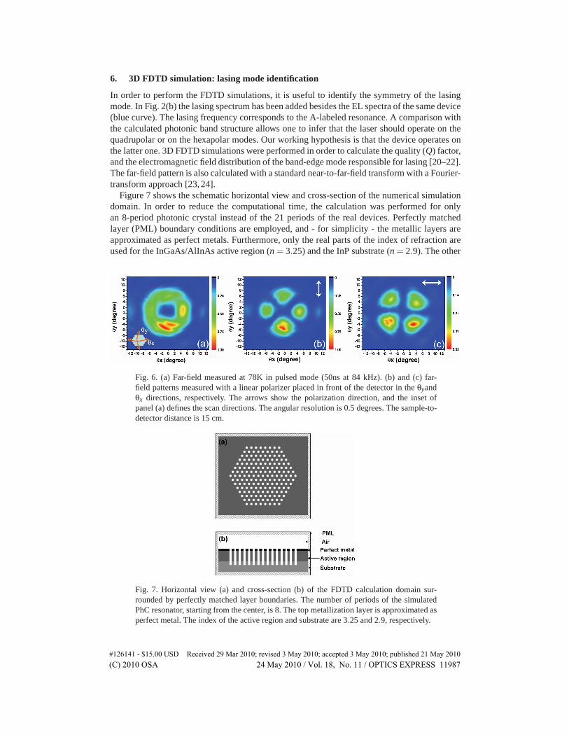
In order to perform the FDTD simulations, it is useful to identify the symmetry of the lasingmode. In Fig. 2(b) the lasing spectrum has been added besides the EL spectra of the same device(blue curve). The lasing frequency corresponds to the A-labeled resonance. A comparison withthe calculated photonic band structure allows one to infer that the laser should operate on thequadrupolar or on the hexapolar modes. Our working hypothesis is that the device operates onthe latter one. 3D FDTD simulations were performed in order to calculate the quality (Q) factor,and the electromagnetic field distribution of the band-edge mode responsible for lasing [20–22].The far-field pattern is also calculated with a standard near-to-far-field transform with a Fourier-transform approach [23, 24].
Figure 7 shows the schematic horizontal view and cross-section of the numerical simulationdomain. In order to reduce the computational time, the calculation was performed for onlyan 8-period photonic crystal instead of the 21 periods of the real devices. Perfectly matchedlayer (PML) boundary conditions are employed, and - for simplicity - the metallic layers areapproximated as perfect metals. Furthermore, only the real parts of the index of refraction areused for the InGaAs/AlInAs active region (n = 3.25) and the InP substrate (n = 2.9). The other
Fig. 6. (a) Far-field measured at 78K in pulsed mode (50ns at 84 kHz). (b) and (c) far-field patterns measured with a linear polarizer placed in front of the detector in the θyandθx directions, respectively. The arrows show the polarization direction, and the inset ofpanel (a) defines the scan directions. The angular resolution is 0.5 degrees. The sample-to-detector distance is 15 cm.
Fig. 7. Horizontal view (a) and cross-section (b) of the FDTD calculation domain sur-rounded by perfectly matched layer boundaries. The number of periods of the simulatedPhC resonator, starting from the center, is 8. The top metallization layer is approximated asperfect metal. The index of the active region and substrate are 3.25 and 2.9, respectively.
#126141 - $15.00 USD Received 29 Mar 2010; revised 3 May 2010; accepted 3 May 2010; published 21 May 2010(C) 2010 OSA 24 May 2010 / Vol. 18, No. 11 / OPTICS EXPRESS 11987
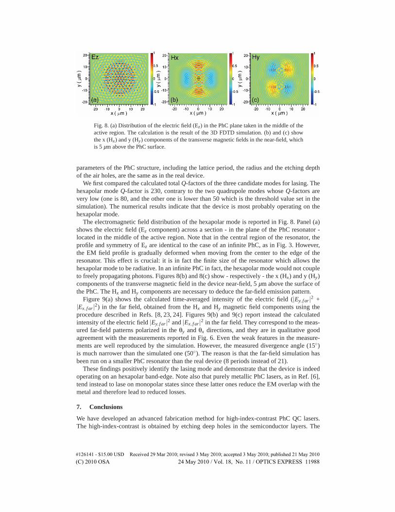
Fig. 8. (a) Distribution of the electric field (Ez) in the PhC plane taken in the middle of theactive region. The calculation is the result of the 3D FDTD simulation. (b) and (c) showthe x (Hx) and y (Hy) components of the transverse magnetic fields in the near-field, whichis 5 µm above the PhC surface.
parameters of the PhC structure, including the lattice period, the radius and the etching depthof the air holes, are the same as in the real device.
We first compared the calculated total Q-factors of the three candidate modes for lasing. Thehexapolar mode Q-factor is 230, contrary to the two quadrupole modes whose Q-factors arevery low (one is 80, and the other one is lower than 50 which is the threshold value set in thesimulation). The numerical results indicate that the device is most probably operating on thehexapolar mode.
The electromagnetic field distribution of the hexapolar mode is reported in Fig. 8. Panel (a)shows the electric field (Ez component) across a section - in the plane of the PhC resonator -located in the middle of the active region. Note that in the central region of the resonator, theprofile and symmetry of Ez are identical to the case of an infinite PhC, as in Fig. 3. However,the EM field profile is gradually deformed when moving from the center to the edge of theresonator. This effect is crucial: it is in fact the finite size of the resonator which allows thehexapolar mode to be radiative. In an infinite PhC in fact, the hexapolar mode would not coupleto freely propagating photons. Figures 8(b) and 8(c) show - respectively - the x (Hx) and y (Hy)components of the transverse magnetic field in the device near-field, 5 µm above the surface ofthe PhC. The Hx and Hy components are necessary to deduce the far-field emission pattern.
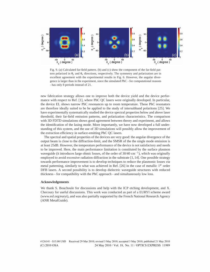
Figure 9(a) shows the calculated time-averaged intensity of the electric field (|Ey, f ar|2 +|Ex, f ar|2) in the far field, obtained from the Hx and Hy magnetic field components using theprocedure described in Refs. [8, 23, 24]. Figures 9(b) and 9(c) report instead the calculatedintensity of the electric field |Ey, f ar|2 and |Ex, f ar|2 in the far field. They correspond to the meas-ured far-field patterns polarized in the θy and θx directions, and they are in qualitative goodagreement with the measurements reported in Fig. 6. Even the weak features in the measure-ments are well reproduced by the simulation. However, the measured divergence angle (15◦)is much narrower than the simulated one (50◦). The reason is that the far-field simulation hasbeen run on a smaller PhC resonator than the real device (8 periods instead of 21).
These findings positively identify the lasing mode and demonstrate that the device is indeedoperating on an hexapolar band-edge. Note also that purely metallic PhC lasers, as in Ref. [6],tend instead to lase on monopolar states since these latter ones reduce the EM overlap with themetal and therefore lead to reduced losses.
7. Conclusions
We have developed an advanced fabrication method for high-index-contrast PhC QC lasers.The high-index-contrast is obtained by etching deep holes in the semiconductor layers. The
#126141 - $15.00 USD Received 29 Mar 2010; revised 3 May 2010; accepted 3 May 2010; published 21 May 2010(C) 2010 OSA 24 May 2010 / Vol. 18, No. 11 / OPTICS EXPRESS 11988
Fig. 9. (a) Calculated far-field pattern. (b) and (c) show the component of the far-field pat-tern polarized in θy and θx directions, respectively. The symmetry and polarization are inexcellent agreement with the experimental results in Fig. 6. However, the angular diver-gence is larger than in the experiment, since the simulated PhC - for computational reasons- has only 8 periods instead of 21.
new fabrication strategy allows one to improve both the device yield and the device perfor-mance with respect to Ref. [1], where PhC QC lasers were originally developed. In particular,the device EL shows narrow PhC resonances up to room temperature. These PhC resonatorsare therefore ideally suited to be be applied to the study of intersubband polaritons [25]. Wehave experimentally systematically studied the device spectral properties below and above laserthreshold, their far-field emission patterns, and polarization characteristics. The comparisonwith 3D FDTD simulations shows good agreement between theory and experiment, and allowsthe identification of the lasing mode. More importantly, we have now developed a full under-standing of this system, and the use of 3D simulations will possibly allow the improvement ofthe extraction efficiency in surface-emitting PhC QC lasers.
The spectral and spatial properties of the devices are very good: the angular divergence of theoutput beam is close to the diffraction-limit, and the SMSR of the the single mode emission isat least 25dB. However, the temperature performance of the device is not satisfactory and needsto be improved. Here, the main performance limitation is constituted by the surface plasmonwaveguide (it introduces large ohmic losses, of the order of 30/40 cm−1), which was originallyemployed to avoid excessive radiation diffraction in the substrate [1,14]. One possible strategytowards performance improvement is to develop techniques to reduce the plasmonic losses viametal patterning, similarly to what was achieved in Ref. [26] in the case of metallic 1st orderDFB lasers. A second possibility is to develop dielectric waveguide structures with reducedthickness - for compatibility with the PhC approach - and simultaneously low loss.
Acknowledgements
We thank S. Bouchoule for discussions and help with the ICP etching development, and X.Checoury for useful discussions. This work was conducted as part of a EURYI scheme award(www.esf.org/euryi), and was also partially supported by the French National Research Agency(ANR MetalGuide).
#126141 - $15.00 USD Received 29 Mar 2010; revised 3 May 2010; accepted 3 May 2010; published 21 May 2010(C) 2010 OSA 24 May 2010 / Vol. 18, No. 11 / OPTICS EXPRESS 11989