Surface Finish Optimization in Electrical Discharge Machining Alberto Gonçalves do Poço Thesis to obtain the Master of Science Degree in Mechanical Engineering Supervisors: Prof. Pedro Alexandre Rodrigues Carvalho Rosa Prof. José Duarte Ribeiro Marafona Examination Committee Chairperson: Prof. Rui Manuel dos Santos Oliveira Baptista Supervisor: Prof. Pedro Alexandre Rodrigues Carvalho Rosa Members of the Committee: Prof. José Firmino Aguilar Madeira Eng. Afonso José de Vilhena Leitão Gregório June 2018
Transcript
Surface Finish Optimization in Electrical Discharge
Machining
Alberto Gonçalves do Poço
Thesis to obtain the Master of Science Degree in
Mechanical Engineering
Supervisors: Prof. Pedro Alexandre Rodrigues Carvalho Rosa
Prof. José Duarte Ribeiro Marafona
Examination Committee
Chairperson: Prof. Rui Manuel dos Santos Oliveira Baptista
Supervisor: Prof. Pedro Alexandre Rodrigues Carvalho Rosa
Members of the Committee: Prof. José Firmino Aguilar Madeira
Eng. Afonso José de Vilhena Leitão Gregório
June 2018
II
III
Resumo
O processo de eletroerosão tem um importante papel no sector dos moldes, cunhos e
cortantes, e na indústria em geral, complementando as tecnologias convencionais no fabrico de
componentes metálicos de precisão. A presente investigação procura identificar os parâmetros
operativos que controlam o acabamento superficial e determinar qual a combinação destes parâmetros
que permite minimizar a rugosidade das superfícies maquinadas. Esta investigação experimental tem
por base a maquinagem do AA1050 A com eléctrodo-ferramenta em cobre eletrolítico em regime de
acabamento. Os principais parâmetros operativos em análise foram a corrente e tempo de pulso. Os
resultados mostram que a rugosidade superficial diminui com a energia de descarga, associada à
redução simultânea da corrente e tempo da descarga. Adicionalmente, a rugosidade do elétrodo-
ferramenta mostra também influenciar a rugosidade da superfície maquinada na peça.
Palavras-Chave: Eletroerosão, Otimização, Rugosidade, Influência da Rugosidade do
Eléctrodo.
IV
Abstract
Electrical Discharge Machining plays an important role in the sector of molds, dies and cutters,
and in the industry overall, being a complement to conventional technologies in the manufacture of
precision metallic components. The current research seeks to identify the operating parameters that
control the surface finish and establish which should be the combination of parameters that allows to
minimize the roughness of the machined surfaces. This experimental research is based on the
machining of AA1050 A with electrolytic copper tool-electrode in finishing operations. The main operative
parameters in question were the current and pulse on time. The results show that the superficial
roughness declined with the discharge energy, associated with the current simultaneous reduction and
the discharge time. In addition, the electrode roughness also shows influence on the machined surface
Neste espaço pretendo prestar os meus sinceros agradecimentos às pessoas que me ajudaram
ao longo deste percurso, pela partilha de conhecimentos e amizade.
Em primeiro lugar agradeço ao meu orientador, Professor Pedro Rosa, pela excelente
orientação, motivação e conhecimento transmitido. Um agradecimento também ao Professor José
Marafona, coorientador desta tese pelos conhecimentos transmitidos.
À equipa do NOF, por todos os esclarecimentos que dizem respeito à componente técnica da
tese, e a amizade desenvolvida nestes meses de trabalho.
À minha família e à Verónica, por toda e qualquer razão.
VI
Contents Resumo ................................................................................................................................................. III
Abstract ................................................................................................................................................. IV
Acknowledgements .............................................................................................................................. V
Contents ................................................................................................................................................ VI
List of Figures ...................................................................................................................................... VII
List of Tables ......................................................................................................................................... X
Abbreviations ........................................................................................................................................ XI
List of Symbols .................................................................................................................................... XII
Figure 2-4 - (a) Gap voltage and current waveform [2]; (b) Actual profile of single EDM pulse [3]. ....... 4
Figure 2-5 – (a) Material removal rate behaviour when subjected to different levels of dielectric pressure
and peak current; (b) Surface roughness when subjected to different levels of dielectric pressure and
peak current; (c) Material removal rate behaviour when subjected to different levels of tool diameter and
peak current; Tool wear rate behaviour when subjected to different levels of tool diameter and peak
current [10]. ............................................................................................................................................. 6
Figure 2-6 – (a) Influence of the heat source parameters on material removal rate [11] and (b)
Relationship between the MRR and EDM parameters [12]. ................................................................... 7
Figure 2-7 - Electrode wear in x and y directions [13]. ............................................................................ 7
Figure 2-8 - Relationship of current with electrode wear; (a) along the width, (b) along the length [13]. 8
Figure 2-9 - Relationship of current with wear ration (V=10) [13]. .......................................................... 9
Figure 2-10 - Relationship between the average white layer and EDM parameters [12]. ...................... 9
Figure 2-11 - Several profiles presented on a machined surface. ........................................................ 10
Figure 2-12 - (a) Arithmetical mean roughness; (b) Mean roughness depth. ....................................... 10
Figure 2-13 - (a) Variation of Ra with discharge current for various hard steels using Cu electrodes
[15]; (b) Relationship between the surface roughness and EDM parameters [12]. .............................. 10
Figure 2-14 - Task Manager on EDM optimization study (adapted from [4]). ....................................... 12
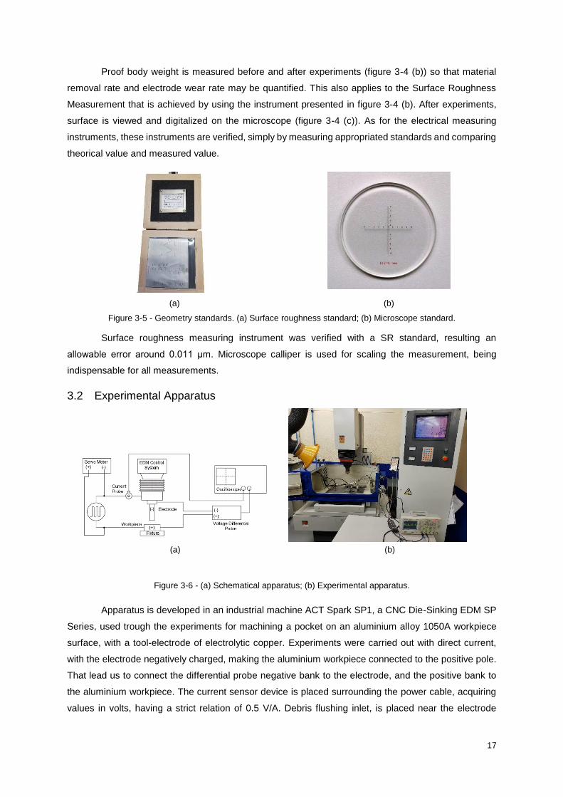
Figure 3-1 – (a) Die-Sinker EDM Act Spark SP1; (b) Electrode and workpiece in their fixtures; (c) Proof
Figure 3-8 - (a) Machined workpiece surface and (b) its respective electrical signature. ..................... 18
Figure 4-1 - Relationship between 𝑅𝑎𝑊 and electrical parameters, for an open voltage of 80 V and
pulse off time of 3 μs. ........................................................................................................................... 23
Figure 4-2 - Relationship between 𝑅𝑧𝑊 and electrical parameters, for an open voltage of 80 V and
pulse off time of 3 μs. ............................................................................................................................ 23
VIII
Figure 4-3 - Relationship between 𝑅𝑎𝑊 and 𝑅𝑎𝑊 ................................................................................ 24
Figure 4-4 - Relationship between 𝑅𝑎𝐸𝑓 and electrical parameters, for an open voltage of 80 V and
pulse off time of 3 μs. ............................................................................................................................ 24
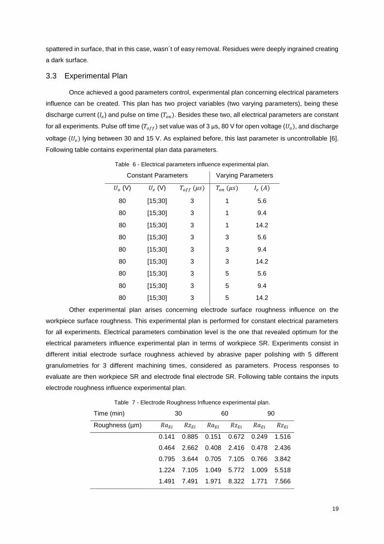
Figure 4-5 - Relationship between 𝑅𝑧𝐸𝑓 and electrical parameters, for an open voltage of 80 V and
pulse off time of 3 μs. ............................................................................................................................ 25
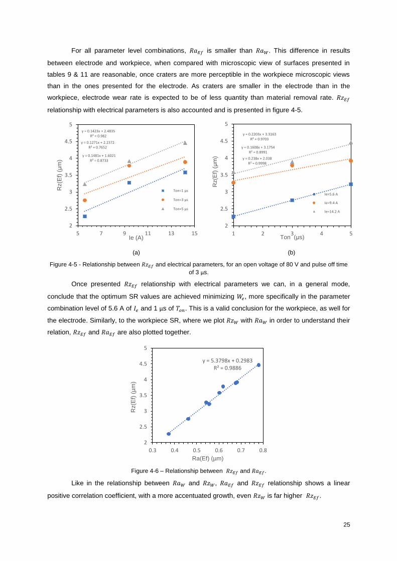
Figure 4-6 – Relationship between 𝑅𝑧𝐸𝑓 and 𝑅𝑎𝐸𝑓. ........................................................................... 25
Figure 4-7 - Relationship between MRR and electrical parameters, for an open voltage of 80 V and
pulse off time of 3 μs. ............................................................................................................................ 26
Figure 4-8 - Relationship between EWR and electrical parameters, for an open voltage of 80 V and
pulse off Time of 3 μs. ........................................................................................................................... 26
Figure 4-9 - Relationship between WR and electrical parameters, for an open voltage of 80 V and
pulse off time of 3 μs. ............................................................................................................................ 27
Figure 4-10 – (a) & (b) S/N plot and (c) & (d) Data means for WR. ...................................................... 28
Figure 4-11 – Proof body after machining for an experiment of 90 minutes with a rough electrode. (a)
Electrode after machining; (b) Workpiece machined surface. ............................................................... 30
Figure 4-26 - Proof body aesthetics for the multiple electrical signatures experiment. (a) Workpiece
machined surface and (b) Electrode machined surface. ....................................................................... 42
Figure 4-27 - Proof body microscopic view for the multiple electrical signature experiments. (a)
Workpiece machined surface and (b) Electrode machined surface. Note, global scale dimension equal
to 0.25 mm. ............................................................................................................................................ 43
IX
Figure 4-28 - Microscopic view of machined surfaces. (a) Workpiece machined surface for single
electrical signature; (b) Workpiece machined surface for multiple electrical signatures. Note, global
scale dimension equal to 0.1 mm. ......................................................................................................... 43
X
List of Tables
Table 1 - Design of Experiments based on a L9 orthogonal array. ...................................................... 11
Table 2 - Experimental Plan Sketch. .................................................................................................... 13
Table 3 - AA 1050 chemical composition. ............................................................................................ 14
Table 4 - Physical properties and Erosion Index of the Proof Body. .................................................... 14
Table 9 - Workpiece microscopic view for the different electrical parameters. Note, real width dimension
equal to 0.25 mm. .................................................................................................................................. 21
Table 10 - Workpiece aesthetics for the different electrical parameters. ............................................. 21
Table 11 - Electrode microscopic view for the different electrical parameters. Note, real width dimension
equal to 0.25 mm. .................................................................................................................................. 22
Table 12 - Electrodes surface after machining for the different electrode parameters. ....................... 22
Table 13 - Electrode Roughness Influence Experimental Plan and respective data. .......................... 29
Material thermal properties play important role on EDM, since material is removed once it melts and
vaporizes from gap region. The combined value of thermal conductivity, specific heat and melting
temperature describe an erosion resistance index [8]. It can be calculated by equation 2:
𝐶𝑚 = 𝜆𝐶𝑝𝑇𝑚2 (2)
where λ is the heat conductivity [W 𝑚−1 𝐾−1], 𝐶𝑝 is the specific heat [J 𝑚−3 𝐾−1] and 𝑇𝑚 is the
melting point [K]. Workpiece material used, shall be of smaller index than materials used for the
electrodes in order to have a reasonable relative wear between electrode and workpiece.
Dielectric fluid properties during the process, can significantly influence process responses, like
surface roughness, material removal rate, etc. Dielectric fluids used on EDM are characterized by
having a high dielectric strength and fast deionization the moment pulse ends [9]. Dielectric pressure
has been used as project variable on EDM Optimization studies, together with electrical and non-
electrical parameters. Figures 2-5 (a)-(d) are quote from a Balasubramanian’s study concerning four
project variables being these peak current, pulse on time, dielectric pressure and tool diameter.
Balasubramanian concluded that material removal rate and tool wear rate are increased whenever
dielectric pressure, peak current and dielectric pressure are increased. For surface roughness, optimum
value is achieved by an intermediate value of peak current and dielectric pressure being least affected
by tool diameter [10].
6
(a) (b)
(c) (d)
Figure 2-5 – (a) Material removal rate behaviour when subjected to different levels of dielectric pressure and peak
current; (b) Surface roughness when subjected to different levels of dielectric pressure and peak current; (c)
Material removal rate behaviour when subjected to different levels of tool diameter and peak current; Tool wear
rate behaviour when subjected to different levels of tool diameter and peak current [10].
2.3 Process Responses
This document studies the influence of determined parameters that characterize the material
removal mechanism by Electrical Discharge Machining on surface roughness. This work gives special
attention to the workpiece surface roughness, but also to quantify material removal rate and electrode
wear rate. This subchapter concerns the main process responses.
2.3.1 Material Removal Rate
Material removal rate expresses the material removed per unit of time. This factor is extremely
important, because it defines a production rate or how fast we can process materials. This can be
calculated by measuring initial and final weight of the workpiece and dividing its difference by machining
time. The following mathematical expression is used to calculate MRR value:
𝑀𝑅𝑅 =𝐼𝑛𝑖𝑡𝑖𝑎𝑙𝑊𝑒𝑖𝑔ℎ𝑡 − 𝐹𝑖𝑛𝑎𝑙𝑊𝑒𝑖𝑔ℎ𝑡
𝑀𝑎𝑐ℎ𝑖𝑛𝑖𝑛𝑔𝑇𝑖𝑚𝑒
[𝑔
𝑚𝑖𝑛]
(3)
𝑀𝑅𝑅 =𝐼𝑛𝑖𝑡𝑖𝑎𝑙𝑉𝑜𝑙𝑢𝑚𝑒 − 𝐹𝑖𝑛𝑎𝑙𝑉𝑜𝑙𝑢𝑚𝑒
𝑀𝑎𝑐ℎ𝑖𝑛𝑖𝑛𝑔𝑇𝑖𝑚𝑒
[𝑚𝑚3
𝑚𝑖𝑛]
(4)
7
To quantify MRR, measuring the specimens weight, is more accurate, in order to avoid
measuring errors, being this approach used on this study. MRR has been mostly studied related to
discharge current and pulse on time, because these are which mainly influence this process response.
Although electrical parameters have a relationship with discharge energy there is a tendency to evaluate
each of them separately for 𝐼𝑒 and 𝑡𝑒 , because these have different effects on the process response.
The following graphs presented in figure 2-6 concern the relationship between MRR and electrical
parameters.
(a) (b)
Figure 2-6 – (a) Influence of the heat source parameters on material removal rate [11] and (b) Relationship between the MRR and EDM parameters [12].
Figure 2-6 (a) deals with an influence study of 𝑊𝑒 on MRR performed by [11], where he
evaluates 𝐼𝑒 and 𝑇𝑜𝑛 separately, like the one presented by [12] in figure 2-6 (b). There is a general
conclusion common to both, that for increasing 𝐼𝑒 leads to higher MRR for a constant 𝑇𝑜𝑛 (𝑡𝑖 in figure 2-
6 (a)), where [12] that the gradual increase of 𝑇𝑜𝑛 doesn´t necessarily improve MRR. On the other hand,
[11] refers that after 𝐼𝑒 at 30 A (15 A/cm2), MRR starts to decrease due to the increase of discharge
current is limited by the current density.
2.3.2 Electrode Wear Rate
Figure 2-7 - Electrode wear in x and y directions [13].
Electrode Wear Rate expresses the electrode wear per unit of time. This can be calculated by
measuring initial and final weight of the electrode and dividing its difference by machining time. EWR
can be calculated by equations 5 and 6:
8
𝐸𝑊𝑅 =𝐼𝑛𝑖𝑡𝑖𝑎𝑙𝑊𝑒𝑖𝑔ℎ𝑡 − 𝐹𝑖𝑛𝑎𝑙𝑊𝑒𝑖𝑔ℎ𝑡
𝑀𝑎𝑐ℎ𝑖𝑛𝑖𝑛𝑔_𝑇𝑖𝑚𝑒 [
𝑔
𝑚𝑖𝑛]
(5)
𝐸𝑊𝑅 =𝐼𝑛𝑖𝑡𝑖𝑎𝑙𝑉𝑜𝑙𝑢𝑚𝑒 − 𝐹𝑖𝑛𝑎𝑙𝑉𝑜𝑙𝑢𝑚𝑒
𝑀𝑎𝑐ℎ𝑖𝑛𝑖𝑛𝑔_𝑇𝑖𝑚𝑒 [
𝑚𝑚3
𝑚𝑖𝑛]
(6)
Excessive electrode wear may cause unallowable defects, such as errors out of the dimensional
tolerance range. A factor commonly used, is also the Wear Ratio or Relative Wear, that stands for the
ratio between EWR and MRR. This concept is traduced in the percentage of material wasted on tool
electrode for removing a certain quantity of material of a workpiece in process. Its mathematical
expression is following presented:
𝑊𝑅 =𝐸𝑊𝑅
𝑀𝑅𝑅
(7)
Where WR, stands for the wear ratio; EWR is the electrode wear rate [g/min]; and MRR stands
for material removal rate [g/min]. Figure 2-8 is quote from a study performed by Khan, concerning
discharge current influence on electrode wear rate.
(a) (b)
Figure 2-8 - Relationship of current with electrode wear; (a) along the width, (b) along the length [13].
Khan [13] considers not only the volumetric electrode wear but width and length dimensions
where he denotes that it is not uniform in terms of width or length directions, being of higher value wear
in width direction, due to the fact a smaller cross section allows a lower heat transfer than a larger cross
section. His general conclusion about electrode wear rate is that it increases with discharge current.
Furthermore, he accounts in his study WR, referring that is known that the current increase beside of
the EWR decrease, induces MRR to increase. Figure 2-9 gathers his WR values where he concludes
that the current increase leads WR to decrease.
9
Figure 2-9 - Relationship of current with wear ration (V=10) [13].
2.3.3 Surface Condition
An important factor that also characterizes EDM performance is surface integrity. As presented
before, in figure 2-1 (b), there are several layers that compose the surface machined by EDM. According
to [14], this has three different surface layers, a first composed by molten and expelled material from
both workpiece and electrode during the erosion process that spatter the surface, followed by the second
layer, called white layer, where its metallurgical structure has been altered by violent temperature
increase and decrease during the erosive process. Third and last layer is the heat affected zone,
consequence of the EDM heating action. Lee [12] refers that predicting white layer thickness is a must,
in order to avoid dimensional errors in the project phase. This is presented in the following figure 2-10,
that contains the white layer thickness behaviour for different levels of 𝐼𝑒 and 𝑇𝑜𝑛, where he concludes
in a general way that its thickness increases for higher levels of 𝐼𝑒 and 𝑇𝑜𝑛 [12].
Figure 2-10 - Relationship between the average white layer and EDM parameters [12].
An important response to any manufacturing process is surface roughness that is a frequent
project requirement and may appear in any technical drawing. Surface roughness is described to be
the sum of irregularities that characterize a surface, due to the manufacturing process and errors of
microgeometry, typical behavior of the surface of a certain material and can be defined in many different
terms. A surface is composed for different profiles (figure 2-11). Roughness or primary texture is the
set of irregularities caused by the manufacturing process, which are the impressions left by the tool (A),
Secondary ripple or texture is the set of irregularities caused by vibrations or deflections of the
production system or the heat treatment (B); Irregular orientation is the general direction of the texture
components (C).
10
Figure 2-11 - Several profiles presented on a machined surface.
This study gives attention to the arithmetical mean roughness (Ra), described by EN ISO 4287
to be the arithmetical mean of the absolute values of the profile deviations (yi) from the mean line of the
roughness profile (Figure 2-12 (a)). It can be calculated by the following mathematical expression:
𝑅𝑎 =1
𝑙𝑚∫ 𝑦(𝑥)𝑑𝑥
𝑙𝑚
0
(8)
(a) (b)
Figure 2-12 - (a) Arithmetical mean roughness; (b) Mean roughness depth.
Average distribution of vertical surface (mean roughness depth, Rz) stands for the average of
5 distances measured from peak to valley in the measured length, illustrated in figure 2-12 (b). This is
then an average of 5 peak to valley distances. Graphs presented in figure 2-13 consider two different
studies. The first presented by [15], figure 2-13 (a), concerning Ra behaviour when subjected to different
intensities of current. His results and conclusions are in conformity with [7]’s assumption above
presented, and in a certain way with the second presented by [12], figure 2-13 (b), that surface
roughness increases gradually with discharge current increase [15].
(a) (b)
Figure 2-13 - (a) Variation of Ra with discharge current for various hard steels using Cu electrodes [15]; (b) Relationship between the surface roughness and EDM parameters [12].
11
Lee [12] concludes that SR increases with discharge current for a constant pulse-on duration.
It may be observed in figure 2-13 (b) that for a certain 𝑇𝑜𝑛, roughness starts to decrease. This turning
point is not common to every 𝐼𝑒 series. The same happened for his results for MRR, where he refers
this dramatic decrease is due to the expansion of plasma channel.
2.3.4 Process Responses Optimization
Electrical Discharge Machining has been one of the main target machining technologies used
as optimization case study, since there is no consolidated theory in this material removal mechanism
relating its waveform, electrical parameters and non-electrical parameters to the different process
responses. Optimization studies are normally based on Taguchi Design of Experiments, where
experiments number depend mainly on the project variables number as well for the levels of each
variable. Experiments in Taguchi design are of smaller number, than the ones on traditional analysis
where, for example, in a design with three variables with three operative levels, 9 experiments are
enough for evaluate the design, and are based on a L9 orthogonal array.
Table 1 - Design of Experiments based on a L9 orthogonal array.
Exp Nº A B C
1 1 1 1
2 1 2 2
3 1 3 3
4 2 1 2
5 2 2 3
6 2 3 1
7 3 1 3
8 3 2 1
9 3 3 2
Table previously presented, sketches a DOE with 3 project variables, A, B and C, where each
of them has 3 operative levels, 1, 2, 3. Taguchi analysis is then based on Signal-to-Noise ratio correlation
functions, and Mean Data of each level, seeking the optimum parameter combination level for a certain
process response. A proper task manager on optimization study is following presented, quote from
Gaikwad EDM optimization study.
12
Figure 2-14 - Task Manager on EDM optimization study (adapted from [4]).
Optimum parameters combination levels shall be identified for the typical Taguchi signal-to-
noise ratio equations, “smaller-the-better” in case we are looking for the combination that minimize a
certain process response, following presented labelled with number (9), and “larger-the-better”, for the
one that maximizes a certain objective function, labelled with number (10), where 𝑛 is number of
observations on a certain process response, and 𝑦 is the response value. These equations are defined
in a way that for both objectives larger S/N ratio value indicates our optimum result.
𝑠
𝑁= −10 log10 (
∑ (𝑦𝑖2)𝑛
𝑖
𝑛) ;
(9)
𝑠
𝑁= −10 log10 (
∑ (1/𝑦𝑖2)𝑛
𝑖
𝑛) ;
(10)
Mean Data is simply calculated as the average response of a certain level of a project variable.
For example, looking to table 1, level 1 of variable A appears in the first 3 experiments. Thus, mean data
response will be the sum of experiment nº1, 2 and 3, divided by three. Three main EDM process
responses on optimization studies are MRR, EWR and SR, and obviously, there isn´t an optimal
parameter combination common to each of these, once maximum MRR is achieved for higher discharge
energy levels that consequently lead to higher EWR, as well for a higher Ra because craters will be of
higher depth and diameter. As explained before, optimal points are identified by S/N ratio and mean
response data of each variable operative level, that generally result on a parameter combination level
that was not covered up by the experimental plan. With this, we proceed to the field of confirmation
tests. Based on mean response levels, results can be predicted in terms of the different EDM process
responses. Predicted response value may be calculated by the following equation:
13
𝛼𝑝𝑟𝑒𝑑𝑖𝑐𝑡𝑒𝑑 = 𝛼𝑚 + ∑(𝛼0 − 𝛼𝑚)
𝑛
𝑖=1
(11)
Where 𝛼𝑝𝑟𝑒𝑑𝑖𝑐𝑡𝑒𝑑 is the value of response at the resulted optimum parameter combination levels,
to predict and validate the EDM process, 𝛼0 is the mean data of a certain response at optimal parameter
level of the factors, and 𝛼𝑚 is the average value of response and n is the number of factors [16].
Experimental plan on this work is a typical DOE of Taguchi Design, based on L9 orthogonal array with
three levels and two factors. The same as in table 1, but with a absent third parameter, shown in table
2.
Table 2 - Experimental Plan Sketch.
Exp Nº A B
1 1 1
2 1 2
3 1 3
4 2 1
5 2 2
6 2 3
7 3 1
8 3 2
9 3 3
This approach was chosen, in order to avoid some erroneous conclusions and clearly evaluate
discharge current and pulse on time influence on the typical EDM process responses.
14
3 Experimental Development
The present work studies the material pair of electrolytic copper and aluminium alloy 1050 A
machinability in finishing operations. This is a typical material choice, aluminium for its relative low
density and price, and electrolytic copper due to its electrical and thermal conductivity, being a preferable
electrode material for a case study. This proof body was processed in Mechanical Technology
Laboratory, in a total of 35 electrodes and 35 workpieces. Dimensions chosen for electrodes geometry
were 30x30x5 𝑚𝑚3, and 25x25x20 𝑚𝑚3 for aluminium workpieces. Following table contains Aluminium
1050 A chemical composition.
Table 3 - AA1050 A chemical composition.
(%) Si Fe Cu Mn Mg Zn Ti Al V Others
AA
1050A
EAA
0.25
max
0.40
max
0.05
max
0.05
max
0.05
max
0.07
max
0.05
max
99.5
min - 0.03
As presented in process parameters section, material thermal properties play a role as non-
electrical parameters, where Reynaerts defines an Erosion Resistance Index. Properties that compose
Erosion Index are Specific Heat, Thermal Conductivity and Melting Point. Table 4 presents the proof
body’s physical properties and respective erosion index.
Table 4 - Physical properties and Erosion Index of the Proof Body.
Properties/Materials AA1050 A Copper
Melting point [K] 923 1356
Specific Heat [J/(kg.K)] 900 381
Thermal Conductivity
[W/(m.K)] 231 392
Density [Kg/m³] 2700 8910
Index Cm [𝐽2/(m.s.kg)] 1.771E+11 2.75E+11
As Reynaerts presents, a high Cm leads us to a fine electrode material, and a low Cm to a fine
workpiece material. Looking at the previews table, we denote that aluminium has a lower Cm than
copper. Aluminium has a high Thermal Conductivity and Specific Heat, making difficult a fast
temperature increase, on the other hand, Aluminium melting point is around 650 ºC, lower than other
workpieces like Steel. Dielectric Fluid used for experiments was a Castrol Ilocut EDM 200 with typical
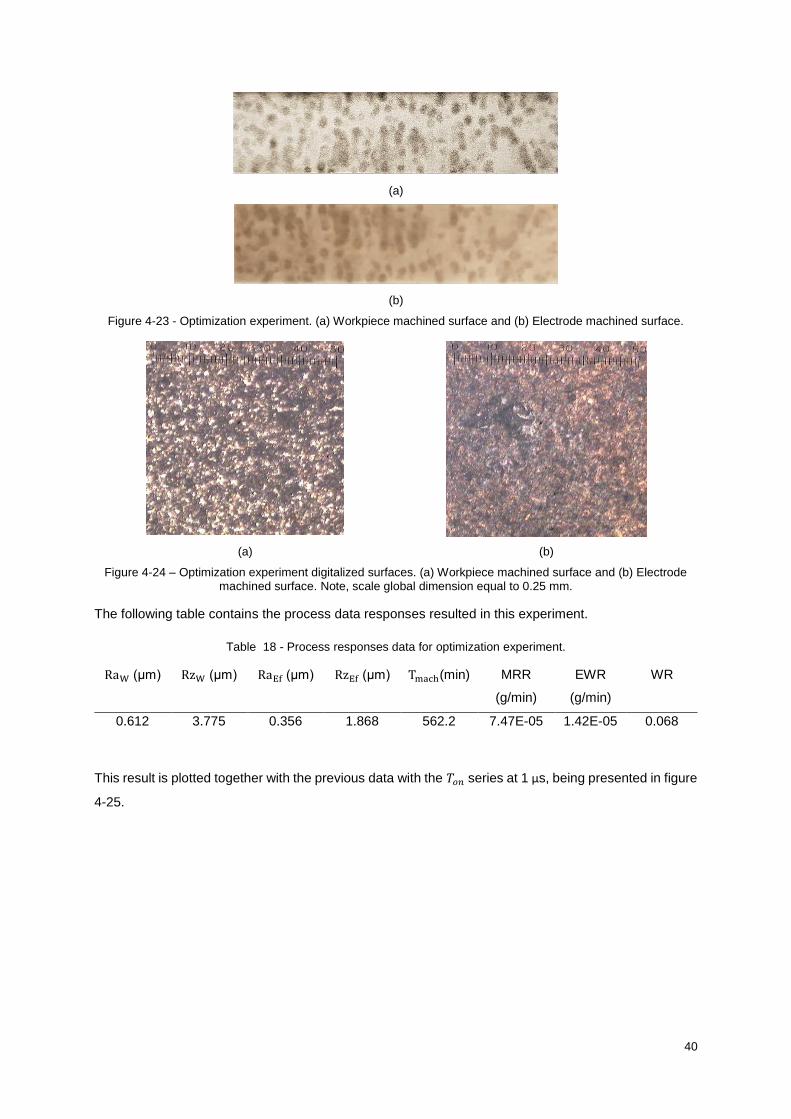
The figures following presented, show the proof body aesthetics for the experiment performed
with multiple electrical signatures.
(a)
(b)
Figure 4-26 - Proof body aesthetics for the multiple electrical signatures experiment. (a) Workpiece machined surface and (b) Electrode machined surface.
Even with this machining strategy, some black dots appear on the machined surfaces proof body. These
are of significative less number than in the previous experiment with a single electrical signature,
because its machining time was far lower.
43
(a) (b)
Figure 4-27 - Proof body microscopic view for the multiple electrical signature experiments. (a) Workpiece machined surface and (b) Electrode machined surface. Note, global scale dimension equal to 0.25 mm.
Summarily, this subchapter presents a method to achieve a fine surface finish together with a
better material removal rate. It is also an empirical optimization, because by analysing electrical
parameters influence experiments we concluded by graphical observation as well with Data Means and
Signal to Noise Correlation function that the lower levels of discharge current and pulse on time lead to
a better surface finish quality. Now comparing tables 18 and 20 data, we denote a general smaller
increase in terms of SR, around 0.1 μm in 𝑅𝑎𝑊, but main point of comparison is the reduced machining
time from 9.5 hours to 20 minutes, that consequently increases MRR. EWR increases with this lower
machining time, but WR is reduced by 0.016. Besides the greater number of black spots appearing on
the workpiece for a single electrical signature, figure 4-28 (a), it presents more uniform craters dimension
than figure 4-28 (b). Following table compares the microscopic view of the single electrical signature
with the one with multiple signatures in a more amplified window on microscope.
(a) (b)
Figure 4-28 - Microscopic view of machined surfaces. (a) Workpiece machined surface for single electrical signature; (b) Workpiece machined surface for multiple electrical signatures. Note, global scale dimension equal
to 0.1 mm.
44
5 Conclusions and future work
This aluminium alloy has shown to be of worse machinability than other typical material used in
Electrical Discharge Machining. To justify this affirmation, we have the lower MRR and higher EWR,
WR, and Ra. This was foreseen, once aluminium erosion index is higher than steel (as example), where
even with a lower Melting Point, it has a high Specific Heat and Thermal Conductivity. These two
properties induce in lower temperatures increase, and that is reflected on MRR, EWR and consequently
in WR. It is important to refer that a lot of preliminary experiments were performed in order to find a
suitable region of parameters to present experiments on electrical parameters experiments sub chapter.
Optimum electrical parameters level combination was identified to be at lower discharge current and
pulse on time, at 5.6 A and 1 µs in terms of global SR and EWR. On the other hand, MRR is identified
to be at the higher lower discharge current and pulse on time, at 14.2 A and 5 µs. Mean level of discharge
current and pulse on time at 5 µs revealed optimum for WR. By empirical optimization, discharge current
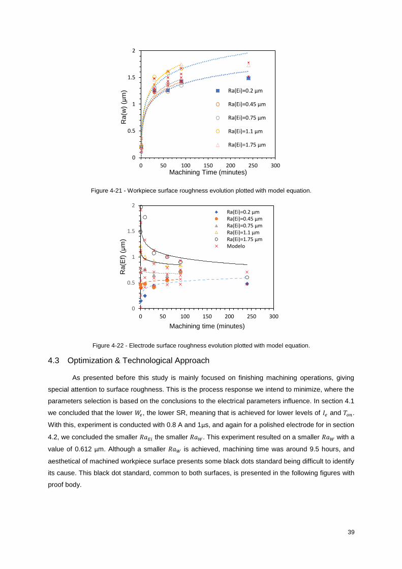
was reduced to 0.8 A achieving a Ra value of 0.612 µm, where MRR dramatically decreased due to the
increased machining time of 9.5 hours. Also, this experiment resulted on a poor aesthetics view with an
ingrained black dot standard printed on both electrode and workpiece surfaces. Machining strategy with
multiple electrical signatures above explained, proved itself useful decreasing machining time to 20
minutes and reducing significantly the number of black dots.
In terms of Electrode Roughness influence, levels of stability, increases and decreases were
identified, a non-electrical parameter that was not found in any study on bibliography. It was decided to
see if there was any influence because in theoretical articles there was always a reference that the
inverted geometry is gradually printed in the workpiece [2]. There was a strict relation between Electrode
and Workpiece Roughness, and it may be seen in figure 4-11. Three regions were identified, where at
first roughness was steady, at a second stage where it presents an approximately linear growth and at
last it tends to stabilize. Polished electrodes revealed to increase their roughness, with the increase of
machining time, while the opposite occurred for rougher electrodes. Initial Electrode Roughness
comprehended between 0.7 and 0.8 µm present a constant evolution with no significant variation
between Ra values while increasing machining time.
For future works, cylindrical shaped electrodes can be used as case study, where these can be
obtained by lathe machining. Performing a facing operation with a controlled tool feed speed will lead to
a more accurate electrode SR value. By varying tool feed speed other SR series can be achieved. Also,
a more uniform surface can be obtained where SR will be radial distributed and of easier concentric
measuring with a surface roughness measuring instrument.
45
Bibliography
[1] – Society of Manufacturing Engineers, 1996.
https://www.sme.org/WorkArea/DownloadAsset.aspx?id=63975. Consulted on 12-03-2018
[2] - Kunieda M., Lauwers B., Rajurkar KP, Schumacher B.M., Advancing EDM through fundamental
insight into the process, Annals of the CIRP, (2005), 54, 599-622.