KEMET’s High Temperature surface mount C0G Multilayer Ceramic Capacitors (MLCCs) are constructed of a robust and proprietary C0G/NP0 base metal electrode (BME) dielectric system that offers industry-leading performance at extreme temperatures up to 200°C. These devices are specifically designed to withstand the demands of harsh industrial environments such as down-hole oil exploration and automotive/avionics engine compartment circuitry.
KEMET’s High Temperature C0G capacitors are temperature compensating and are well suited for resonant circuit applications or those where Q and stability of capacitance characteristics are required. They exhibit no change in capacitance with respect to time and voltage and boast a negligible change in capacitance with reference to ambient temperature. Capacitance change is limited to ±30ppm/ºC from −55°C to +200°C. In addition, these capacitors exhibit high insulation resistance with low dissipation factor at
elevated temperatures up to 200°C. They also exhibit low ESR at high frequencies and offer greater volumetric efficiency over competitive high temperature precious metal electrode (PME) and BME ceramic capacitor devices.
These devices are Lead (Pb)-Free, RoHS and REACH compliant without the need of any exemptions.
Surface Mount Multilayer Ceramic Chip Capacitors (SMD MLCCs)
High Temperature 200°C, C0G Dielectric, 10 – 200 VDC(Industrial Grade)
1 Additional capacitance tolerance offerings may be available. Contact KEMET for details.2 Additional termination finish options may be available. Contact KEMET for details.
Surface Mount Multilayer Ceramic Chip Capacitors (SMD MLCCs)High Temperature (200°C), C0G Dielectric, 10 – 200 VDC (Industrial Grade)
Benefits
• −55°C to +200°C operating temperature range• Lead (Pb)-free, RoHS and REACH compliant• EIA 0402, 0603, 0805, 1206, 1210, 1812, and 2220
case sizes• DC voltage ratings of 10 V, 16 V, 25 V, 50 V, 100 V,
and 200 V• Capacitance offerings ranging from 0.5 pF up to 470 nF • Available capacitance tolerances of ±0.10 pF, ±0.25 pF,
±0.5 pF, ±1%, ±2%, ±5%, ±10% or ±20%• No piezoelectric noise• Extremely low ESR and ESL• High thermal stability• High ripple current capability
• Preferred capacitance solution at line frequencies and into the MHz range
• No capacitance change with respect to applied rated DC voltage
• Negligible capacitance change with respect to temperature from −55°C to +200°C
• No capacitance decay with time• Non-polar device, minimizing installation concerns• 100% pure matte tin-plated termination finish allowing for
excellent solderability• Gold (Au), Tin/Lead (Sn/Pb) and 100% pure matte Tin (Sn)
termination finishes available
Applications
Typical applications include critical timing, tuning, circuits requiring low loss, circuits with pulse, high current, decoupling, bypass, filtering, transient voltage suppression, blocking and energy storage for use in extreme environments such as down-hole exploration, aerospace engine compartments and geophysical probes.
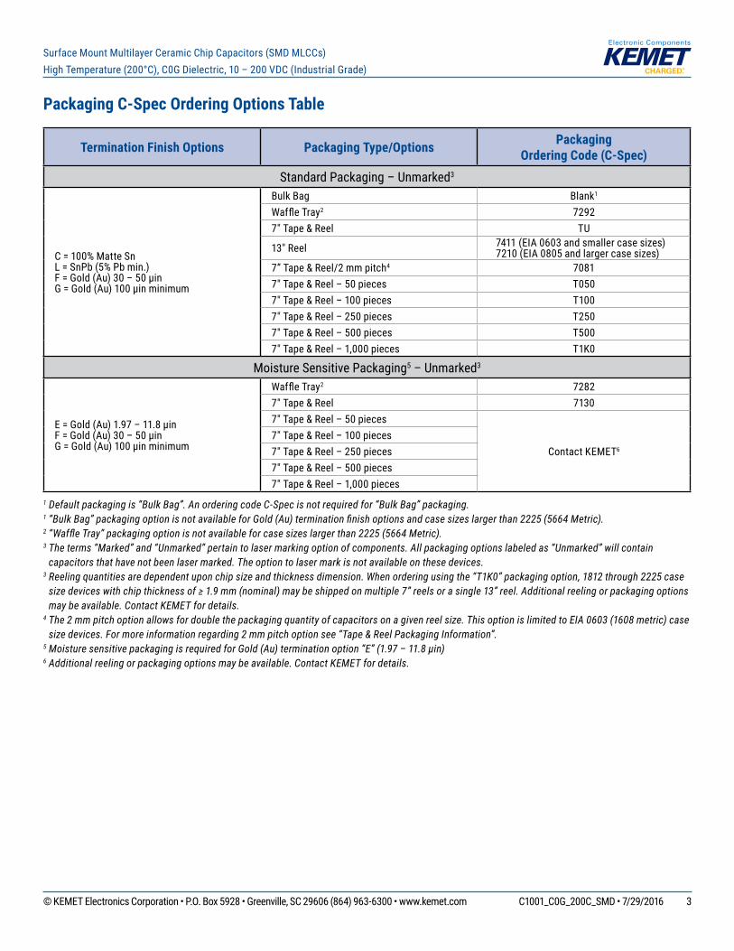
1 Default packaging is “Bulk Bag”. An ordering code C-Spec is not required for “Bulk Bag” packaging.1 “Bulk Bag” packaging option is not available for Gold (Au) termination finish options and case sizes larger than 2225 (5664 Metric).2 “Waffle Tray” packaging option is not available for case sizes larger than 2225 (5664 Metric).3 The terms “Marked” and “Unmarked” pertain to laser marking option of components. All packaging options labeled as “Unmarked” will contain
capacitors that have not been laser marked. The option to laser mark is not available on these devices.3 Reeling quantities are dependent upon chip size and thickness dimension. When ordering using the “T1K0” packaging option, 1812 through 2225 case
size devices with chip thickness of ≥ 1.9 mm (nominal) may be shipped on multiple 7” reels or a single 13” reel. Additional reeling or packaging options may be available. Contact KEMET for details.
4 The 2 mm pitch option allows for double the packaging quantity of capacitors on a given reel size. This option is limited to EIA 0603 (1608 metric) case size devices. For more information regarding 2 mm pitch option see “Tape & Reel Packaging Information”.
5 Moisture sensitive packaging is required for Gold (Au) termination option “E” (1.97 – 11.8 µin)6 Additional reeling or packaging options may be available. Contact KEMET for details.
Solder Wave or Solder Reflow0805 2012 2.00 (0.079)
±0.20 (0.008)1.25 (0.049)
±0.20 (0.008)0.50 (0.02)
±0.25 (0.010) 0.75 (0.030)
1206 3216 3.20 (0.126) ±0.20 (0.008)
1.60 (0.063) ±0.20 (0.008)
0.50 (0.02) ±0.25 (0.010)
N/A1210 3225 3.20 (0.126)
±0.20 (0.008)2.50 (0.098)
±0.20 (0.008)0.50 (0.02)
±0.25 (0.010)Solder Reflow
Only1812 4532 4.50 (0.177) ±0.30 (0.012)
3.20 (0.126) ±0.30 (0.012)
0.60 (0.024) ±0.35 (0.014)
2220 5650 5.70 (0.224) ±0.40 (0.016)
5.00 (0.197) ±0.40 (0.016)
0.60 (0.024) ±0.35 (0.014)
Qualification/Certification
High temperature (200ºC) Industrial grade products meet or exceed the requirements outlined in Table 4, Performance & Reliability. Qualification packages are available for review and download on our website at www.kemet.com/hightemp
Environmental Compliance
Lead (Pb)-free, RoHS, and REACH compliant without exemptions (excluding SnPb termination finish option).
1Dielectric Withstanding Voltage (DWV) 250% of rated voltage (5±1 seconds and charge/discharge not exceeding 50 mA)
2Dissipation Factor (DF) Maximum Limit at 25ºC 0.1%
3Insulation Resistance (IR) Minimum Limit at 25°C 1,000 megohm microfarads or 100 GΩ (Rated voltage applied for 120±5 seconds at 25°C)
1 DWV is the voltage a capacitor can withstand (survive) for a short period of time. It exceeds the nominal and continuous working voltage of the capacitor.
2 Capacitance and dissipation factor (DF) measured under the following conditions: 1 MHz ±100 kHz and 1.0 ±0.2 Vrms if capacitance ≤ 1,000 pF 1 kHz ±50 Hz and 1.0 ±0.2 Vrms if capacitance > 1,000 pF3 To obtain IR limit, divide MΩ-µF value by the capacitance and compare to GΩ limit. Select the lower of the two limits. Note: When measuring capacitance it is important to ensure the set voltage level is held constant. The HP4284 & Agilent E4980 have a feature known as Automatic Level Control (ALC). The ALC feature should be switched to “ON.”
Post Environmental Limits
High Temperature Life, Biased Humidity, Moisture Resistance
DielectricRated DCVoltage
CapacitanceValue
Dissipation Factor (Maximum %)
CapacitanceShift
Insulation Resistance
C0G All All 0.5 0.3% or ±0.25 pF 10% of Initial Limit
Capacitance Tolerance Product Availability and Chip Thickness CodesSee Table 2 for Chip Thickness Dimensions
0.5 & 0.75 pF 508 & 758 B C D BB BB BB BB CF CF CF CF CF CF DN DN DN DN DN DN1.0 - 9.0 pF* 109 - 919* B C D BB BB BB BB CF CF CF CF CF CF DN DN DN DN DN DN EB EB EB EB EB EB10 - 91 pF* 100 - 910* F G J K M BB BB BB BB CF CF CF CF CF CF DN DN DN DN DN DN EB EB EB EB EB EB
100 - 180 pF* 101 - 181* F G J K M BB BB BB BB BB CF CF CF CF CF CF DN DN DN DN DN DN EB EB EB EB EB EB200 - 430 pF* 201 - 431* F G J K M BB BB BB BB BB CF CF CF CF CF DN DN DN DN DN DN EB EB EB EB EB EB
470 pF 471 F G J K M BB BB BB BB BB CF CF CF CF CF DN DN DN DN DN DP EB EB EB EB EB EB510 pF 511 F G J K M BB BB BB BB BB CF CF CF CF CF DN DN DN DN DN DN EB EB EB EB EB EB560 pF 561 F G J K M BB BB BB BB BB CF CF CF CF CF DN DN DN DN DN DN EB EB EB EB EB EB620 pF 621 F G J K M BB BB BB BB BB CF CF CF CF CF DN DN DN DN DN DN EB EB EB EB EB EB680 pF 681 F G J K M BB BB BB BB BB CF CF CF CF CF DN DN DN DN DN DN EB EB EB EB EB EB750 pF 751 F G J K M BB BB BB BB BB CF CF CF CF CF DN DN DN DN DN DN EB EB EB EB EB EB820 pF 821 F G J K M BB BB BB BB BB CF CF CF CF CF DN DN DN DN DN DN EB EB EB EB EB EB910 pF 911 F G J K M BB BB BB BB BB CF CF CF CF CF DN DN DN DN DP DP EB EB EB EB EB EB
1,000 pF 102 F G J K M BB BB BB BB BB CF CF CF CF CF DN DN DN DN DP DP EB EB EB EB EB EE1,100 pF 112 F G J K M BB BB BB BB CF CF CF CF CF DN DN DN DN DN EB EB EB EB EB EB1,200 pF 122 F G J K M BB BB BB BB CF CF CF CF CF DN DN DN DN DN EB EB EB EB EB EB1,300 pF 132 F G J K M BB BB BB BB CF CF CF CF CF DP DP DP DP DP EB EB EB EB EC EC1,500 pF 152 F G J K M BB BB BB BB CF CF CF CF CF DP DP DP DP DP EB EB EB EB ED EC1,600 pF 162 F G J K M CF CF CF CF CF DP DP DP DP DP EB EB EB EB ED ED1,800 pF 182 F G J K M CF CF CF CF CF DP DP DP DP DP EB EB EB EB ED ED2,000 pF 202 F G J K M CF CF CF CF CF DN DN DN DN DN EB EB EB EB ED ED2,200 pF 222 F G J K M CF CF CF CF CF DN DN DN DN DN EB EB EB EB EE EE2,400 pF 242 F G J K M CF CF CF CF CF DN DN DN DN DN EB EB EB EB EC EC2,700 pF 272 F G J K M CF CF CF CF CF DN DN DN DN DN EB EB EB EB EC EC3,000 pF 302 F G J K M CF CF CF CF CF DP DP DP DP DN EC EC EC EC EC3,300 pF 332 F G J K M CF CF CF CF CF DP DP DP DP DN EC EC EC EC EE3,600 pF 362 F G J K M CF CF CF CF CF DP DP DP DP DN EC EC EC EC EE3,900 pF 392 F G J K M CF CF CF CF CF DE DE DE DE DN EC EC EC EC EF4,300 pF 432 F G J K M CF CF CF CF CF DE DE DE DE DN EC EC EC EC EC4,700 pF 472 F G J K M CF CF CF CF CF DE DE DE DE DN EC EC EC EC EC5,100 pF 512 F G J K M CF CF CF CF DE DE DE DE DN ED ED ED ED ED5,600 pF 562 F G J K M CF CF CF CF DN DN DN DN DN ED ED ED ED ED6,200 pF 622 F G J K M CF CF CF CF DN DN DN DN DN EB EB EB EB EB6,800 pF 682 F G J K M CF CF CF CF DN DN DN DN DN EB EB EB EB EB7,500 pF 752 F G J K M CF CF CF DN DN DN DN DN EB EB EB EB EB8,200 pF 822 F G J K M CF CF CF DN DN DN DN DN EC EC EC EC EB9,100 pF 912 F G J K M CF CF CF DN DN DN DN DN EC EC EC EC EB
10,000 pF 103 F G J K M CF CF CF DN DN DN DN DP ED ED ED ED EB12,000 pF 123 F G J K M DN DN DN DN DE EB EB EB EB EB15,000 pF 153 F G J K M DN DN DN DP DG EB EB EB EB EB18,000 pF 183 F G J K M DN DN DN DP EB EB EB EB EB22,000 pF 223 F G J K M DP DP DP DF EB EB EB EB EC27,000 pF 273 F G J K M DF DF DF EB EB EB EB EE33,000 pF 333 F G J K M DG DG DG EB EB EB EB EE39,000 pF 393 F G J K M DG DG DG EC EC EC EE EH47,000 pF 473 F G J K M DG DG DG EC EC EC EE EH56,000 pF 563 F G J K M ED ED ED EF68,000 pF 683 F G J K M EF EF EF EH82,000 pF 823 F G J K M EH EH EH EH
*Capacitance range Includes E24 decade values only. (i.e., 10, 11, 12, 13, 15, 16, 18, 20, 22, 24, 27, 30, 33, 36, 39, 43, 47, 51, 56, 62, 68, 75, 82, and 91)KEMET reserves the right to substitute product with an improved temperature characteristic, tighter capacitance tolerance and/or higher voltage capability within the same form factor (configuration and dimensions).These products are protected under US Patents 7,172,985 and 7,670,981, other patents pending, and any foreign counterparts.
*Capacitance range Includes E24 decade values only. (i.e., 10, 11, 12, 13, 15, 16, 18, 20, 22, 24, 27, 30, 33, 36, 39, 43, 47, 51, 56, 62, 68, 75, 82, and 91)KEMET reserves the right to substitute product with an improved temperature characteristic, tighter capacitance tolerance and/or higher voltage capability within the same form factor (configuration and dimensions).These products are protected under US Patents 7,172,985 and 7,670,981, other patents pending, and any foreign counterparts.
Capacitance Tolerance Product Availability and Chip Thickness CodesSee Table 2 for Chip Thickness Dimensions
0.5 & 0.75 pF 508 & 758 B C D1.0 - 9.1 pF* 109 - 919* B C D FB FB FB FB FB FB10 - 91 pF* 100 - 910* F G J K M FB FB FB FB FB FB
100 - 910 pF* 101 - 911* F G J K M FB FB FB FB FB FB1,000 pF 102 F G J K M FB FB FB FB FB FB1,100 pF 112 F G J K M FB FB FB FB FB FB1,200 pF 122 F G J K M FB FB FB FB FB FB1,300 pF 132 F G J K M FB FB FB FB FB FC1,500 pF 152 F G J K M FB FB FB FB FB FE1,600 pF 162 F G J K M FB FB FB FB FB FE1,800 pF 182 F G J K M FB FB FB FB FB FE2,000 pF 202 F G J K M FB FB FB FB FC FE2,200 pF 222 F G J K M FB FB FB FB FC FG2,400 pF 242 F G J K M FB FB FB FB FC FC2,700 pF 272 F G J K M FB FB FB FB FC FC3,000 pF 302 F G J K M FB FB FB FB FC FF3,300 pF 332 F G J K M FB FB FB FB FF FF3,600 pF 362 F G J K M FB FB FB FB FF FF3,900 pF 392 F G J K M FB FB FB FB FF FF4,300 pF 432 F G J K M FB FB FB FB FF FF4,700 pF 472 F G J K M FF FF FF FF FG FG5,100 pF 512 F G J K M FB FB FB FB FG FG5,600 pF 562 F G J K M FB FB FB FB FG FG6,200 pF 622 F G J K M FB FB FB FB FG6,800 pF 682 F G J K M FB FB FB FB FG7,500 pF 752 F G J K M FC FC FC FC FC8,200 pF 822 F G J K M FC FC FC FC FC9,100 pF 912 F G J K M FE FE FE FE FE
10,000 pF 103 F G J K M FF FF FF FF FF12,000 pF 123 F G J K M FG FG FG FG FB15,000 pF 153 F G J K M FG FG FG FG FB GB GB GB GB GB18,000 pF 183 F G J K M FB FB FB FB FB GB GB GB GB GB22,000 pF 223 F G J K M FB FB FB FB FB GB GB GB GB GB27,000 pF 273 F G J K M FB FB FB FB FB GB GB GB GB GB33,000 pF 333 F G J K M FB FB FB FB FB GB GB GB GB GB39,000 pF 393 F G J K M FB FB FB FB FE GB GB GB GB GB47,000 pF 473 F G J K M FB FB FB FB FE GB GB GB GB GB56,000 pF 563 F G J K M FB FB FB FB FF GB GB GB GB GB68,000 pF 683 F G J K M FB FB FB FC FG GB GB GB GB GB82,000 pF 823 F G J K M FC FC FC FF FH GB GB GB GB GB
0.10 µF 104 F G J K M FE FE FE FG FM GB GB GB GB GD0.12 µF 124 F G J K M FG FG FG FH GB GB GB GB GH0.15 µF 154 F G J K M FH FH FH FM GD GD GD GD GN0.18 µF 184 F G J K M GH GH GH GH0.22 µF 224 F G J K M GK GK GK GK0.47 µF 474 F G J K M JJ JJ JJ JJ
Package quantity based on finished chip thickness specifications.1 If ordering using the 2mm Tape and Reel pitch option, the packaging quantity outlined in the table above will be doubled. This option is limited to EIA
0603 (1608 metric) case size devices. For more information regarding 2mm pitch option see “Tape & Reel Packaging Information”.
1 The "Packaging C-Spec" is a 4-digit code which identifies the packaging type. When ordering, the proper code must be included in the 15th through 18th character positions of the ordering code. See "Ordering Information" section of this document for further details. Product ordered without a packaging C-Spec will default to our standard "Bulk Bag" packaging.
2 A packaging C-Spec (see note 1 above) is not required For "Bulk Bag" packaging (excluding Anti-Static Bulk Bag). The 15th through 18th character positions of the ordering code should be left blank. All product ordered without a packaging C-Spec will default to our standard "Bulk Bag" packaging.
3 Also commonly referred to as “Chip Carrier” or “Molded Tray”. All tray packaging options offer static protection.
1 Only for capacitance values ≥ 22 µFDensity Level A: For low-density product applications. Recommended for wave solder applications and provides a wider process window for reflow solder processes. KEMET only recommends wave soldering of EIA 0603, 0805 and 1206 case sizes.Density Level B: For products with a moderate level of component density. Provides a robust solder attachment condition for reflow solder processes.Density Level C: For high component density product applications. Before adapting the minimum land pattern variations the user should perform qualification testing based on the conditions outlined in IPC Standard 7351 (IPC–7351).
Image below based on Density Level B for an EIA 1210 case size.
Surface Mount Multilayer Ceramic Chip Capacitors (SMD MLCCs)High Temperature (200°C), C0G Dielectric, 10 – 200 VDC (Industrial Grade)
Soldering Process
Recommended Soldering Technique: • Solder wave or solder reflow for EIA case sizes 0603, 0805 and 1206 • All other EIA case sizes are limited to solder reflow only
Recommended Reflow Soldering Profile:KEMET’s families of surface mount multilayer ceramic capacitors (SMD MLCCs) are compatible with wave (single or dual), convection, IR or vapor phase reflow techniques. Preheating of these components is recommended to avoid extreme thermal stress. KEMET’s recommended profile conditions for convection and IR reflow reflect the profile conditions of the IPC/ J-STD-020 standard for moisture sensitivity testing. These devices can safely withstand a maximum of three reflow passes at these conditions.
Profile FeatureTermination Finish
SnPb 100% Matte Sn
Preheat/SoakTemperature Minimum (TSmin) 100°C 150°CTemperature Maximum (TSmax) 150°C 200°C
Time (tS) from TSmin to TSmax 60 – 120 seconds 60 – 120 seconds
Moisture Resistance Cycled Temp/RH 0 V, 10 cycles at 24 hours each
Physical, Mechanical & Process Tests per MIL–STD 202/JIS–C–6429
Resistance to Solvents Include Aqueous wash chemical, OKEM Clean or equivalent
Mechanical Shock and Vibration Method 213: Figure 1, Condition F Method 204: 5 gs for 20 minutes 12 cycles
Resistance to Soldering Heat Condition B, no per-heat of samples, Single Wave Solder
Terminal Strength Force of 1.8 kg for 60 seconds
Board Flex Appendix 2, Note: 3.0 mm (minimum)
Storage and Handling
Ceramic chip capacitors should be stored in normal working environments. While the chips themselves are quite robust in other environments, solderability will be degraded by exposure to high temperatures, high humidity, corrosive atmospheres, and long term storage. In addition, packaging materials will be degraded by high temperature–reels may soften or warp and tape peel force may increase. KEMET recommends that maximum storage temperature not exceed 40°C and maximum storage humidity not exceed 70% relative humidity. In addition, temperature fluctuations should be minimized to avoid condensation on the parts and atmospheres should be free of chlorine and sulfur bearing compounds. For optimized solderability chip stock should be used promptly, preferably within the time frame outlined in the table below:
Termination Finish Termination Finish Ordering Code1 Storage Life
100% Matte Tin (Sn) C 1.5 years upon receipt
SnPb (5% Pb min.) L 1.5 years upon receipt
Gold (Au) 1.97 – 11.8 µin2 E 6 months upon receipt2
Gold (Au) 30 – 50 µin F 1.5 years upon receipt
Gold (Au) 100 µin min. G 1.5 years upon receipt
1 The fourteenth (14th) character position of the KEMET part number is assigned to identify and/or define the termination finish. For more information, see “Ordering Information” section of this document.
2 Gold plating option “E” devices should remain in its factory sealed moisture sensitive packaging during storage. If the factory sealed packaging is disturbed please store any remaining packaged components in a dry box container to prevent oxidation of the termination finish.
Surface Mount Multilayer Ceramic Chip Capacitors (SMD MLCCs)High Temperature (200°C), C0G Dielectric, 10 – 200 VDC (Industrial Grade)
Tape & Reel Packaging Information
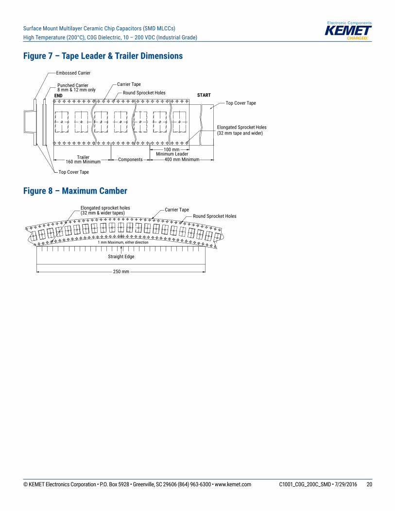
KEMET offers multilayer ceramic chip capacitors packaged in 8, 12 and 16 mm tape on 7" and 13" reels in accordance with EIA Standard 481. This packaging system is compatible with all tape-fed automatic pick and place systems. See Table 2 for details on reeling quantities for commercial chips.
8 mm, 12 mmor 16 mm Carrier Tape 178 mm (7.00")
or330 mm (13.00")
Anti-Static Reel
Embossed Plastic* or Punched Paper Carrier.
Embossment or Punched Cavity
Anti-Static Cover Tape(.10 mm (.004") Maximum Thickness)
Chip and KPS Orientation in Pocket(except 1825 Commercial, and 1825 and 2225 Military)
*EIA 01005, 0201, 0402 and 0603 case sizes available on punched paper carrier only.
B 1 is for tape feeder reference only, including draft concentric about B o.
T 2
ØD 1
ØDo
B 1
S 1
T1
E 1
E 2
P 1
P 2
EmbossmentFor cavity size,see Note 1 Table 4
[10 pitches cumulativetolerance on tape ± 0.2 mm]
Table 6 – Embossed (Plastic) Carrier Tape DimensionsMetric will govern
Constant Dimensions — Millimeters (Inches)
Tape Size D0D1 Minimum
Note 1 E1 P0 P2R Reference
Note 2S1 Minimum
Note 3T
MaximumT1
Maximum
8 mm
1.5+0.10 −0.0 (0.059+0.004 −0.0)
1.0(0.039)
1.75±0.10(0.069±0.004)
4.0±0.10(0.157±0.004)
2.0±0.05(0.079±0.002)
25.0(0.984)
0.600(0.024)
0.600(0.024)
0.100(0.004)12 mm
1.5(0.059)
30(1.181)
16 mm
Variable Dimensions — Millimeters (Inches)
Tape Size Pitch B1 MaximumNote 4
E2 Minimum F P1
T2 Maximum
W Maximum A0,B0 & K0
8 mm Single (4 mm) 4.35 (0.171)
6.25 (0.246)
3.5±0.05 (0.138±0.002)
4.0±0.10(0.157±0.004)
2.5 (0.098)
8.3 (0.327)
Note 512 mm Single (4 mm) & Double (8 mm)
8.2 (0.323)
10.25 (0.404)
5.5±0.05 (0.217±0.002)
8.0±0.10(0.315±0.004)
4.6 (0.181)
12.3 (0.484)
16 mm Triple (12 mm) 12.1 (0.476)
14.25(0.561)
7.5±0.05(0.138±0.002)
12.0±0.10(0.157±0.004)
4.6 (0.181)
16.3 (0.642)
1. The embossment hole location shall be measured from the sprocket hole controlling the location of the embossment. Dimensions of embossment location and hole location shall be applied independent of each other.
2. The tape with or without components shall pass around R without damage (see Figure 6).3. If S1 < 1.0 mm, there may not be enough area for cover tape to be properly applied (see EIA Standard 481 paragraph 4.3 section b).4. B1 dimension is a reference dimension for tape feeder clearance only.5. The cavity defi ned by A0, B0 and K0 shall surround the component with suffi cient clearance that: (a) the component does not protrude above the top surface of the carrier tape. (b) the component can be removed from the cavity in a vertical direction without mechanical restriction, after the top cover tape has been removed. (c) rotation of the component is limited to 20° maximum for 8 and 12 mm tapes and 10° maximum for 16 mm tapes (see Figure 3). (d) lateral movement of the component is restricted to 0.5 mm maximum for 8 and 12 mm wide tape and to 1.0 mm maximum for 16 mm tape
(See Figure 4). (e) for KPS Series product, A0 and B0 are measured on a plane 0.3 mm above the bottom of the pocket. (f) see Addendum in EIA Standard 481 for standards relating to more precise taping requirements.
Table 7 – Punched (Paper) Carrier Tape Dimensions Metric will govern
Constant Dimensions — Millimeters (Inches)Tape Size D0 E1 P0 P2 T1 Maximum G Minimum R Reference
Note 2
8 mm 1.5 +0.10 -0.0 (0.059 +0.004 -0.0)
1.75 ±0.10 (0.069 ±0.004)
4.0 ±0.10 (0.157 ±0.004)
2.0 ±0.05 (0.079 ±0.002)
0.10 (0.004)
Maximum0.75
(0.030) 25
(0.984)
Variable Dimensions — Millimeters (Inches)Tape Size Pitch E2 Minimum F P1 T Maximum W Maximum A0 B0
8 mm Half (2 mm) 6.25 (0.246)
3.5 ±0.05 (0.138 ±0.002)
2.0 ±0.05 (0.079 ±0.002) 1.1
(0.098)
8.3(0.327) Note 1
8 mm Single (4 mm) 4.0 ±0.10 (0.157 ±0.004)
8.3(0.327)
1. The cavity defi ned by A0, B0 and T shall surround the component with suffi cient clearance that: a) the component does not protrude beyond either surface of the carrier tape. b) the component can be removed from the cavity in a vertical direction without mechanical restriction, after the top cover tape has been removed. c) rotation of the component is limited to 20° maximum (see Figure 3). d) lateral movement of the component is restricted to 0.5 mm maximum (see Figure 4). e) see Addendum in EIA Standard 481 for standards relating to more precise taping requirements.2. The tape with or without components shall pass around R without damage (see Figure 6).
Surface Mount Multilayer Ceramic Chip Capacitors (SMD MLCCs)High Temperature (200°C), C0G Dielectric, 10 – 200 VDC (Industrial Grade)
Packaging Information Performance Notes
1. Cover Tape Break Force: 1.0 Kg minimum.2. Cover Tape Peel Strength: The total peel strength of the cover tape from the carrier tape shall be:
Tape Width Peel Strength8 mm 0.1 to 1.0 Newton (10 to 100 gf)
12 and 16 mm 0.1 to 1.3 Newton (10 to 130 gf)
The direction of the pull shall be opposite the direction of the carrier tape travel. The pull angle of the carrier tape shall be 165° to 180° from the plane of the carrier tape. During peeling, the carrier and/or cover tape shall be pulled at a velocity of 300 ±10 mm/minute.3. Labeling: Bar code labeling (standard or custom) shall be on the side of the reel opposite the sprocket holes. Refer to EIA Standards 556 and 624.
1 Packaging of 1206 (3216 metric) case size capacitors is dependent upon the nominal chip thickness of the device. See "Capacitance Range/Selection Waterfall" and "Chip Thickness/Tape & Reel Packaging Quantities" to identify the nominal chip thickness of the capacitor.2 Assigned to 1206 (3216 metric) case size capacitors with nominal thickness of ≤ 1.25mm (0.049 inches).3 Assigned to 1206 (3216 metric) case size capacitors with nominal thickness of > 1.25mm (0.049 inches).
Table 9B – Waffl e Tray Dimensions – Millimeters
Case Size 2" x 2" Waffl e Tray Dimensions – Millimeters Packaging Quantity(pcs/unit
1 Packaging of 1206 (3216 metric) case size capacitors is dependent upon the nominal chip thickness of the device. See "Capacitance Range/Selection Waterfall" and "Chip Thickness/Tape & Reel Packaging Quantities" to identify the nominal chip thickness of the capacitor.2 Assigned to 1206 (3216 metric) case size capacitors with nominal thickness of ≤ 1.25mm (0.049 inches).3 Assigned to 1206 (3216 metric) case size capacitors with nominal thickness of > 1.25mm (0.049 inches).
Surface Mount Multilayer Ceramic Chip Capacitors (SMD MLCCs)High Temperature (200°C), C0G Dielectric, 10 – 200 VDC (Industrial Grade)
KEMET Electronic Corporation Sales Offi ces
For a complete list of our global sales offi ces, please visit www.kemet.com/sales.
DisclaimerAll product specifi cations, statements, information and data (collectively, the “Information”) in this datasheet are subject to change. The customer is responsible for checking and verifying the extent to which the Information contained in this publication is applicable to an order at the time the order is placed.
All Information given herein is believed to be accurate and reliable, but it is presented without guarantee, warranty, or responsibility of any kind, expressed or implied.
Statements of suitability for certain applications are based on KEMET Electronics Corporation’s (“KEMET”) knowledge of typical operating conditions for such applications, but are not intended to constitute – and KEMET specifi cally disclaims – any warranty concerning suitability for a specifi c customer application or use. The Information is intended for use only by customers who have the requisite experience and capability to determine the correct products for their application. Any technical advice inferred from this Information or otherwise provided by KEMET with reference to the use of KEMET’s products is given gratis, and KEMET assumes no obligation or liability for the advice given or results obtained.
Although KEMET designs and manufactures its products to the most stringent quality and safety standards, given the current state of the art, isolated component failures may still occur. Accordingly, customer applications which require a high degree of reliability or safety should employ suitable designs or other safeguards (such as installation of protective circuitry or redundancies) in order to ensure that the failure of an electrical component does not result in a risk of personal injury or property damage.
Although all product–related warnings, cautions and notes must be observed, the customer should not assume that all safety measures are indicted or that other measures may not be required.
KEMET is a registered trademark of KEMET Electronics Corporation.