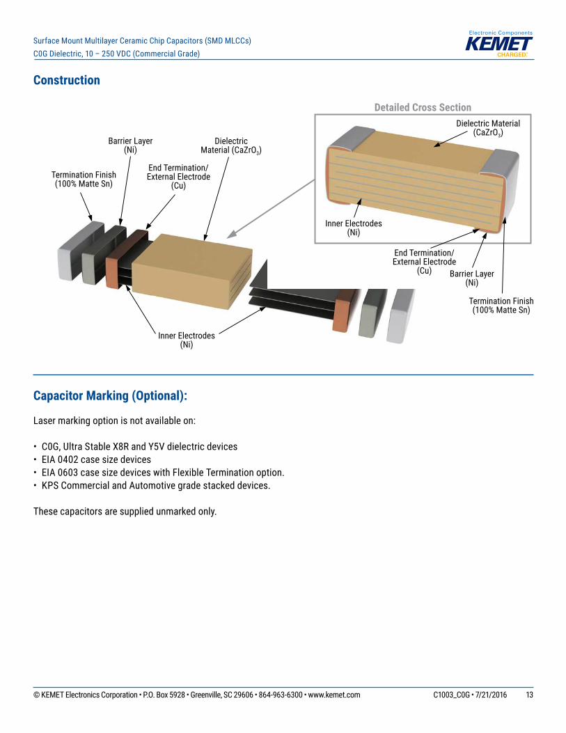
1 Flexible termination option is available. Please see FT-CAP product bulletin C1062_C0G_FT-CAP_SMD2 Additional capacitance tolerance offerings may be available. Contact KEMET for details.3 Additional termination finish options may be available. Contact KEMET for details.
1 Default packaging is “Bulk Bag”. An ordering code C-Spec is not required for “Bulk Bag” packaging.1 The terms “Marked” and “Unmarked” pertain to laser marking option of capacitors. All packaging options labeled as “Unmarked” will contain
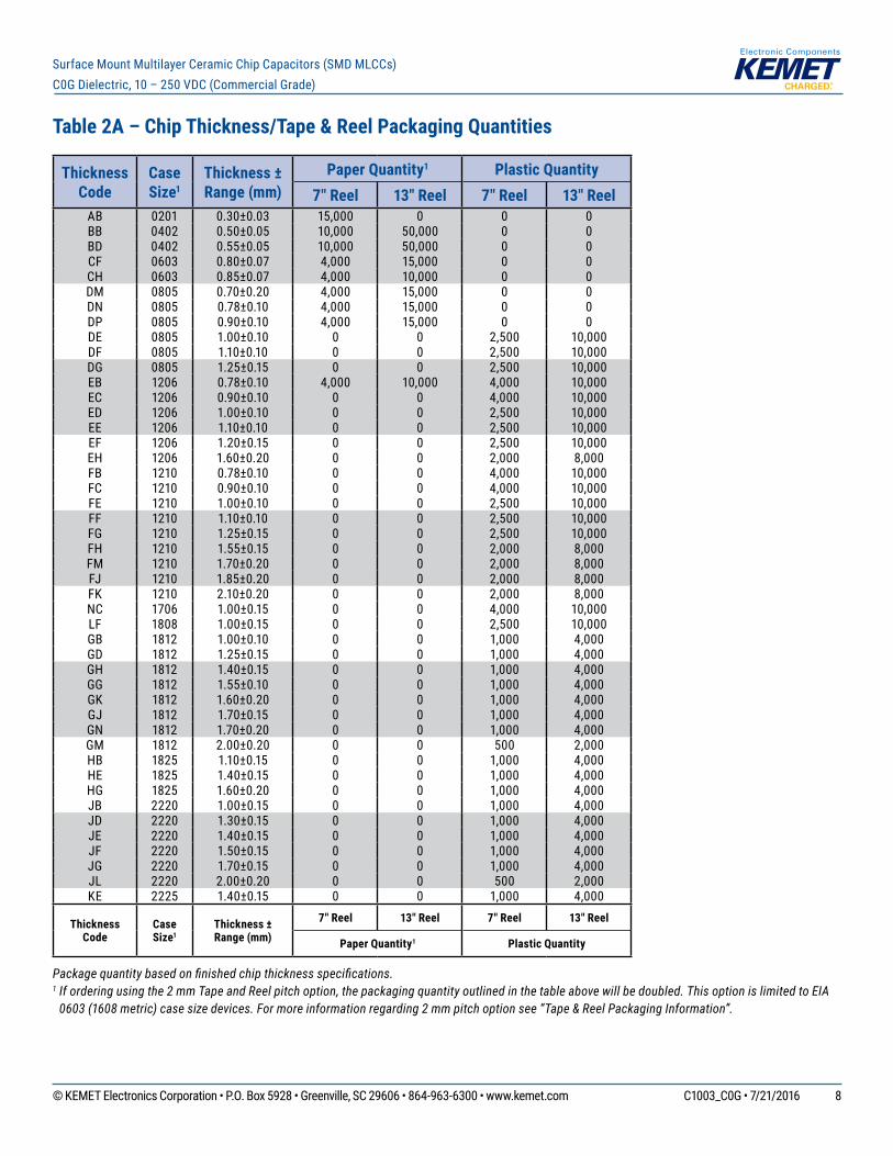
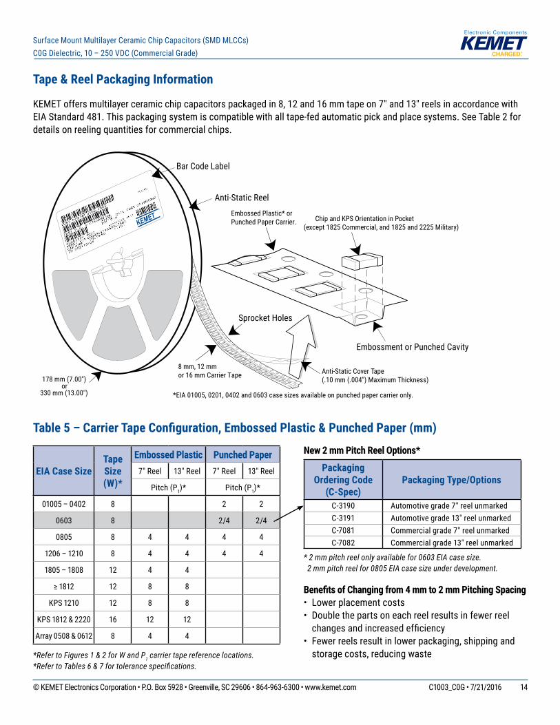
capacitors that have not been laser marked. The option to laser mark is not available on these devices. For more information see “Capacitor Marking”.2 The 2 mm pitch option allows for double the packaging quantity of capacitors on a given reel size. This option is limited to EIA 0603 (1608 metric) case
size devices. For more information regarding 2 mm pitch option see “Tape & Reel Packaging Information”.
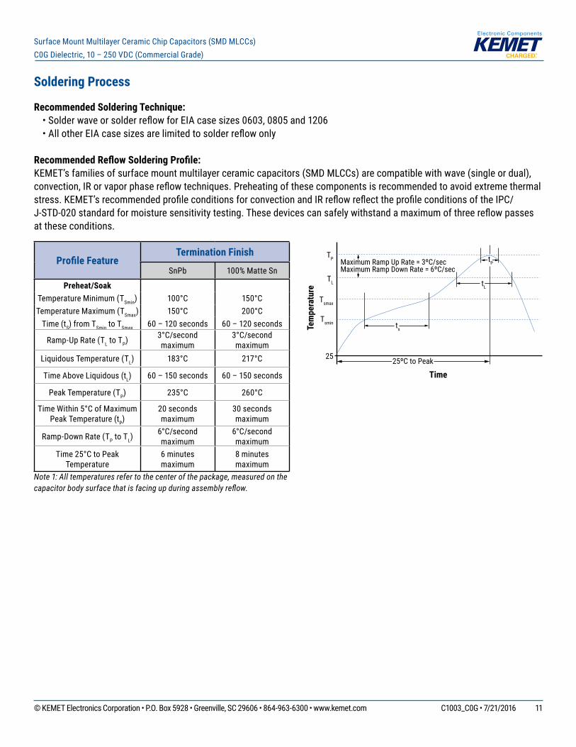
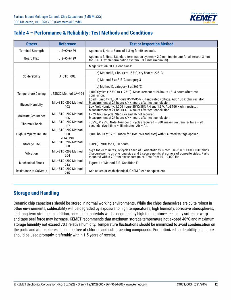
CommercialGradeproductsaresubjecttointernalqualification.Detailsregardingtestmethodsandconditionsarereferenced in Table 4, Performance and Reliability.
1 DWV is the voltage a capacitor can withstand (survive) for a short period of time. It exceeds the nominal and continuous working voltage of the capacitor.
2 Capacitance and dissipation factor (DF) measured under the following conditions: 1 MHz ±100 kHz and 1.0 Vrms ±0.2 V if capacitance ≤ 1,000 pF 1 kHz ±50 Hz and 1.0 Vrms ±0.2 V if capacitance > 1,000 pF
3 To obtain IR limit, divide MΩ-µF value by the capacitance and compare to GΩ limit. Select the lower of the two limits. Capacitance and Dissipation Factor (DF) measured under the following conditions:
Note: When measuring capacitance it is important to ensure the set voltage level is held constant. The HP4284 and Agilent E4980 have a feature known as Automatic Level Control (ALC). The ALC feature should be switched to "ON."
Post Environmental Limits
High Temperature Life, Biased Humidity, Moisture Resistance
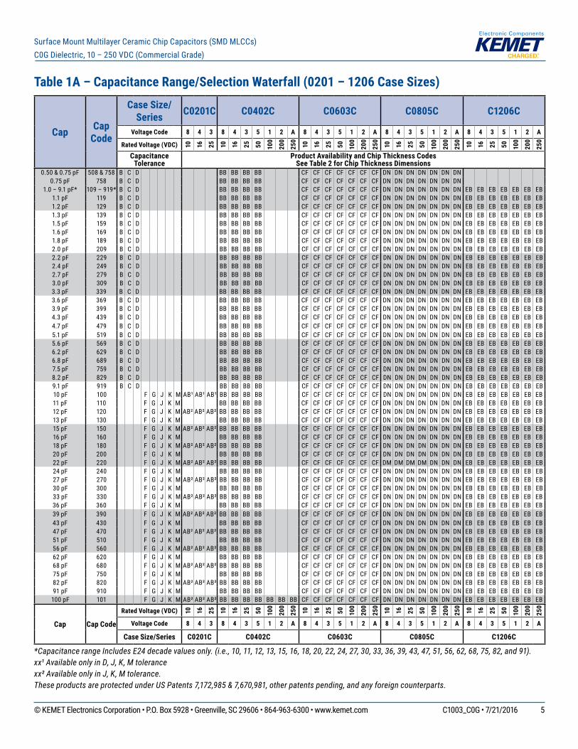
*Capacitance range Includes E24 decade values only. (i.e., 10, 11, 12, 13, 15, 16, 18, 20, 22, 24, 27, 30, 33, 36, 39, 43, 47, 51, 56, 62, 68, 75, 82, and 91).xx¹ Available only in D, J, K, M tolerancexx² Available only in J, K, M tolerance. These products are protected under US Patents 7,172,985 & 7,670,981, other patents pending, and any foreign counterparts.
Cap Cap Code
Case Size/ Series C0201C C0402C C0603C C0805C C1206C
Voltage Code 8 4 3 8 4 3 5 1 2 A 8 4 3 5 1 2 A 8 4 3 5 1 2 A 8 4 3 5 1 2 A
Rated Voltage (VDC) 10 16 25 10 16 25 50 100
200
250
10 16 25 50 100
200
250
10 16 25 50 100
200
250
10 16 25 50 100
200
250
Capacitance Tolerance
Product Availability and Chip Thickness CodesSee Table 2 for Chip Thickness Dimensions
0.50&0.75pF 508&758 B C D BB BB BB BB CF CF CF CF CF CF CF DN DN DN DN DN DN DN0.75pF 758 B C D BB BB BB BB CF CF CF CF CF CF CF DN DN DN DN DN DN DN
1.0–9.1pF* 109–919* B C D BB BB BB BB CF CF CF CF CF CF CF DN DN DN DN DN DN DN EB EB EB EB EB EB EB1.1pF 119 B C D BB BB BB BB CF CF CF CF CF CF CF DN DN DN DN DN DN DN EB EB EB EB EB EB EB1.2pF 129 B C D BB BB BB BB CF CF CF CF CF CF CF DN DN DN DN DN DN DN EB EB EB EB EB EB EB1.3pF 139 B C D BB BB BB BB CF CF CF CF CF CF CF DN DN DN DN DN DN DN EB EB EB EB EB EB EB1.5pF 159 B C D BB BB BB BB CF CF CF CF CF CF CF DN DN DN DN DN DN DN EB EB EB EB EB EB EB1.6pF 169 B C D BB BB BB BB CF CF CF CF CF CF CF DN DN DN DN DN DN DN EB EB EB EB EB EB EB1.8pF 189 B C D BB BB BB BB CF CF CF CF CF CF CF DN DN DN DN DN DN DN EB EB EB EB EB EB EB2.0pF 209 B C D BB BB BB BB CF CF CF CF CF CF CF DN DN DN DN DN DN DN EB EB EB EB EB EB EB2.2pF 229 B C D BB BB BB BB CF CF CF CF CF CF CF DN DN DN DN DN DN DN EB EB EB EB EB EB EB2.4pF 249 B C D BB BB BB BB CF CF CF CF CF CF CF DN DN DN DN DN DN DN EB EB EB EB EB EB EB2.7pF 279 B C D BB BB BB BB CF CF CF CF CF CF CF DN DN DN DN DN DN DN EB EB EB EB EB EB EB3.0pF 309 B C D BB BB BB BB CF CF CF CF CF CF CF DN DN DN DN DN DN DN EB EB EB EB EB EB EB3.3pF 339 B C D BB BB BB BB CF CF CF CF CF CF CF DN DN DN DN DN DN DN EB EB EB EB EB EB EB3.6pF 369 B C D BB BB BB BB CF CF CF CF CF CF CF DN DN DN DN DN DN DN EB EB EB EB EB EB EB3.9pF 399 B C D BB BB BB BB CF CF CF CF CF CF CF DN DN DN DN DN DN DN EB EB EB EB EB EB EB4.3pF 439 B C D BB BB BB BB CF CF CF CF CF CF CF DN DN DN DN DN DN DN EB EB EB EB EB EB EB4.7pF 479 B C D BB BB BB BB CF CF CF CF CF CF CF DN DN DN DN DN DN DN EB EB EB EB EB EB EB5.1pF 519 B C D BB BB BB BB CF CF CF CF CF CF CF DN DN DN DN DN DN DN EB EB EB EB EB EB EB5.6pF 569 B C D BB BB BB BB CF CF CF CF CF CF CF DN DN DN DN DN DN DN EB EB EB EB EB EB EB6.2pF 629 B C D BB BB BB BB CF CF CF CF CF CF CF DN DN DN DN DN DN DN EB EB EB EB EB EB EB6.8pF 689 B C D BB BB BB BB CF CF CF CF CF CF CF DN DN DN DN DN DN DN EB EB EB EB EB EB EB7.5pF 759 B C D BB BB BB BB CF CF CF CF CF CF CF DN DN DN DN DN DN DN EB EB EB EB EB EB EB8.2pF 829 B C D BB BB BB BB CF CF CF CF CF CF CF DN DN DN DN DN DN DN EB EB EB EB EB EB EB9.1pF 919 B C D BB BB BB BB CF CF CF CF CF CF CF DN DN DN DN DN DN DN EB EB EB EB EB EB EB10pF 100 F G J K M AB¹ AB¹ AB¹ BB BB BB BB CF CF CF CF CF CF CF DN DN DN DN DN DN DN EB EB EB EB EB EB EB11pF 110 F G J K M BB BB BB BB CF CF CF CF CF CF CF DN DN DN DN DN DN DN EB EB EB EB EB EB EB12pF 120 F G J K M AB² AB² AB² BB BB BB BB CF CF CF CF CF CF CF DN DN DN DN DN DN DN EB EB EB EB EB EB EB13pF 130 F G J K M BB BB BB BB CF CF CF CF CF CF CF DN DN DN DN DN DN DN EB EB EB EB EB EB EB15pF 150 F G J K M AB² AB² AB² BB BB BB BB CF CF CF CF CF CF CF DN DN DN DN DN DN DN EB EB EB EB EB EB EB16pF 160 F G J K M BB BB BB BB CF CF CF CF CF CF CF DN DN DN DN DN DN DN EB EB EB EB EB EB EB18pF 180 F G J K M AB² AB² AB² BB BB BB BB CF CF CF CF CF CF CF DN DN DN DN DN DN DN EB EB EB EB EB EB EB20pF 200 F G J K M BB BB BB BB CF CF CF CF CF CF CF DN DN DN DN DN DN DN EB EB EB EB EB EB EB22pF 220 F G J K M AB² AB² AB² BB BB BB BB CF CF CF CF CF CF CF DM DM DM DM DN DN DN EB EB EB EB EB EB EB24pF 240 F G J K M BB BB BB BB CF CF CF CF CF CF CF DN DN DN DN DN DN DN EB EB EB EB EB EB EB27pF 270 F G J K M AB² AB² AB² BB BB BB BB CF CF CF CF CF CF CF DN DN DN DN DN DN DN EB EB EB EB EB EB EB30pF 300 F G J K M BB BB BB BB CF CF CF CF CF CF CF DN DN DN DN DN DN DN EB EB EB EB EB EB EB33pF 330 F G J K M AB² AB² AB² BB BB BB BB CF CF CF CF CF CF CF DN DN DN DN DN DN DN EB EB EB EB EB EB EB36pF 360 F G J K M BB BB BB BB CF CF CF CF CF CF CF DN DN DN DN DN DN DN EB EB EB EB EB EB EB39pF 390 F G J K M AB² AB² AB² BB BB BB BB CF CF CF CF CF CF CF DN DN DN DN DN DN DN EB EB EB EB EB EB EB43pF 430 F G J K M BB BB BB BB CF CF CF CF CF CF CF DN DN DN DN DN DN DN EB EB EB EB EB EB EB47pF 470 F G J K M AB² AB² AB² BB BB BB BB CF CF CF CF CF CF CF DN DN DN DN DN DN DN EB EB EB EB EB EB EB51pF 510 F G J K M BB BB BB BB CF CF CF CF CF CF CF DN DN DN DN DN DN DN EB EB EB EB EB EB EB56pF 560 F G J K M AB² AB² AB² BB BB BB BB CF CF CF CF CF CF CF DN DN DN DN DN DN DN EB EB EB EB EB EB EB62pF 620 F G J K M BB BB BB BB CF CF CF CF CF CF CF DN DN DN DN DN DN DN EB EB EB EB EB EB EB68pF 680 F G J K M AB² AB² AB² BB BB BB BB CF CF CF CF CF CF CF DN DN DN DN DN DN DN EB EB EB EB EB EB EB75pF 750 F G J K M BB BB BB BB CF CF CF CF CF CF CF DN DN DN DN DN DN DN EB EB EB EB EB EB EB82pF 820 F G J K M AB² AB² AB² BB BB BB BB CF CF CF CF CF CF CF DN DN DN DN DN DN DN EB EB EB EB EB EB EB91pF 910 F G J K M BB BB BB BB CF CF CF CF CF CF CF DN DN DN DN DN DN DN EB EB EB EB EB EB EB100pF 101 F G J K M AB² AB² AB² BB BB BB BB BB BB BB CF CF CF CF CF CF CF DN DN DN DN DN DN DN EB EB EB EB EB EB EB
Cap Cap Code
Rated Voltage (VDC) 10 16 25 10 16 25 50 100
200
250
10 16 25 50 100
200
250
10 16 25 50 100
200
250
10 16 25 50 100
200
250
Voltage Code 8 4 3 8 4 3 5 1 2 A 8 4 3 5 1 2 A 8 4 3 5 1 2 A 8 4 3 5 1 2 A
Case Size/Series C0201C C0402C C0603C C0805C C1206C
*Capacitance range Includes E24 decade values only. (i.e., 10, 11, 12, 13, 15, 16, 18, 20, 22, 24, 27, 30, 33, 36, 39, 43, 47, 51, 56, 62, 68, 75, 82, and 91).xx¹ Available only in D, J, K, M tolerancexx² Available only in J, K, M tolerance. These products are protected under US Patents 7,172,985 & 7,670,981, other patents pending, and any foreign counterparts.
Cap Cap Code
Case Size/ Series C0201C C0402C C0603C C0805C C1206C
Voltage Code 8 4 3 8 4 3 5 1 2 A 8 4 3 5 1 2 A 8 4 3 5 1 2 A 8 4 3 5 1 2 A
Rated Voltage (VDC) 10 16 25 10 16 25 50 100
200
250
10 16 25 50 100
200
250
10 16 25 50 100
200
250
10 16 25 50 100
200
250
Capacitance Tolerance
Product Availability and Chip Thickness CodesSee Table 2 for Chip Thickness Dimensions
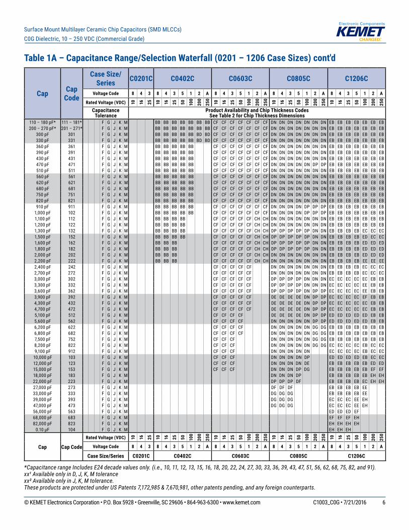
110–180pF* 111–181* F G J K M BB BB BB BB BB BB BB CF CF CF CF CF CF CF DN DN DN DN DN DN DN EB EB EB EB EB EB EB200–270pF* 201–271* F G J K M BB BB BB BB BB BB BB CF CF CF CF CF CF CF DN DN DN DN DN DN DN EB EB EB EB EB EB EB
300pF 301 F G J K M BB BB BB BB BB BD BD CF CF CF CF CF CF CF DN DN DN DN DN DN DN EB EB EB EB EB EB EB330pF 331 F G J K M BB BB BB BB BB BD BD CF CF CF CF CF CF CF DN DN DN DN DN DN DN EB EB EB EB EB EB EB360pF 361 F G J K M BB BB BB BB BB CF CF CF CF CF CF CF DN DN DN DN DN DN DN EB EB EB EB EB EB EB390pF 391 F G J K M BB BB BB BB BB CF CF CF CF CF CF CF DN DN DN DN DN DN DN EB EB EB EB EB EB EB430pF 431 F G J K M BB BB BB BB BB CF CF CF CF CF CF CF DN DN DN DN DN DN DN EB EB EB EB EB EB EB470pF 471 F G J K M BB BB BB BB BB CF CF CF CF CF CF CF DN DN DN DN DN DP DP EB EB EB EB EB EB EB510pF 511 F G J K M BB BB BB BB BB CF CF CF CF CF CF CF DN DN DN DN DN DN DN EB EB EB EB EB EB EB560pF 561 F G J K M BB BB BB BB BB CF CF CF CF CF CF CF DN DN DN DN DN DN DN EB EB EB EB EB EB EB620pF 621 F G J K M BB BB BB BB BB CF CF CF CF CF CF CF DN DN DN DN DN DN DN EB EB EB EB EB EB EB680pF 681 F G J K M BB BB BB BB BB CF CF CF CF CF CF CF DN DN DN DN DN DN DN EB EB EB EB EB EB EB750pF 751 F G J K M BB BB BB BB BB CF CF CF CF CF CF CF DN DN DN DN DN DN DN EB EB EB EB EB EB EB820pF 821 F G J K M BB BB BB BB BB CF CF CF CF CF CF CF DN DN DN DN DN DN DN EB EB EB EB EB EB EB910pF 911 F G J K M BB BB BB BB BB CF CF CF CF CF CF CF DN DN DN DN DP DP DP EB EB EB EB EB EB EB1,000pF 102 F G J K M BB BB BB BB BB CF CF CF CF CF CF CF DN DN DN DN DP DP DP EB EB EB EB EB EB EB1,100pF 112 F G J K M BB BB BB BB CF CF CF CF CF CH CH DN DN DN DN DN DN DN EB EB EB EB EB EB EB1,200pF 122 F G J K M BB BB BB BB CF CF CF CF CF CH CH DN DN DN DN DN DN DN EB EB EB EB EB EB EB1,300pF 132 F G J K M BB BB BB BB CF CF CF CF CF CH CH DP DP DP DP DP DN DN EB EB EB EB EC EC EC1,500pF 152 F G J K M BB BB BB BB CF CF CF CF CF CH CH DP DP DP DP DP DN DN EB EB EB EB ED EC EC1,600pF 162 F G J K M BB BB BB CF CF CF CF CF CH CH DP DP DP DP DP DN DN EB EB EB EB ED ED ED1,800pF 182 F G J K M BB BB BB CF CF CF CF CF CH CH DP DP DP DP DP DN DN EB EB EB EB ED ED ED2,000pF 202 F G J K M BB BB BB CF CF CF CF CF CH CH DN DN DN DN DN DN DN EB EB EB EB ED ED ED2,200pF 222 F G J K M BB BB BB CF CF CF CF CF CH CH DN DN DN DN DN DN DN EB EB EB EB EE EE EE2,400pF 242 F G J K M CF CF CF CF CF DN DN DN DN DN DN DN EB EB EB EB EC EC EC2,700pF 272 F G J K M CF CF CF CF CF DN DN DN DN DN DN DN EB EB EB EB EC EC EC3,000pF 302 F G J K M CF CF CF CF CF DP DP DP DP DN DN DN EC EC EC EC EC EB EB3,300pF 332 F G J K M CF CF CF CF CF DP DP DP DP DN DN DN EC EC EC EC EE EB EB3,600pF 362 F G J K M CF CF CF CF CF DP DP DP DP DN DP DP EC EC EC EC EE EB EB3,900pF 392 F G J K M CF CF CF CF CF DE DE DE DE DN DP DP EC EC EC EC EF EB EB4,300pF 432 F G J K M CF CF CF CF CF DE DE DE DE DN DP DP EC EC EC EC EC EB EB4,700pF 472 F G J K M CF CF CF CF CF DE DE DE DE DN DP DP EC EC EC EC EC EB EB5,100pF 512 F G J K M CF CF CF CF DE DE DE DE DN DP DP ED ED ED ED ED EB EB5,600pF 562 F G J K M CF CF CF CF DN DN DN DN DN DP DP ED ED ED ED ED EB EB6,200pF 622 F G J K M CF CF CF CF DN DN DN DN DN DG DG EB EB EB EB EB EB EB6,800pF 682 F G J K M CF CF CF CF DN DN DN DN DN DG DG EB EB EB EB EB EB EB7,500pF 752 F G J K M CF CF CF DN DN DN DN DN DG DG EB EB EB EB EB EB EB8,200pF 822 F G J K M CF CF CF DN DN DN DN DN DG DG EC EC EC EC EB EC EC9,100pF 912 F G J K M CF CF CF DN DN DN DN DN EC EC EC EC EB EC EC10,000pF 103 F G J K M CF CF CF DN DN DN DN DP ED ED ED ED EB EC EC12,000pF 123 F G J K M CF CF CF DN DN DN DN DE EB EB EB EB EB ED ED15,000pF 153 F G J K M CF CF CF DN DN DN DP DG EB EB EB EB EB EF EF18,000pF 183 F G J K M DN DN DN DP EB EB EB EB EB EH EH22,000pF 223 F G J K M DP DP DP DF EB EB EB EB EC EH EH27,000pF 273 F G J K M DF DF DF EB EB EB EB EE33,000pF 333 F G J K M DG DG DG EB EB EB EB EE39,000pF 393 F G J K M DG DG DG EC EC EC EE EH47,000pF 473 F G J K M DG DG DG EC EC EC EE EH56,000pF 563 F G J K M ED ED ED EF68,000pF 683 F G J K M EF EF EF EH82,000pF 823 F G J K M EH EH EH EH0.10µF 104 F G J K M EH EH EH
Cap Cap Code
Rated Voltage (VDC) 10 16 25 10 16 25 50 100
200
250
10 16 25 50 100
200
250
10 16 25 50 100
200
250
10 16 25 50 100
200
250
Voltage Code 8 4 3 8 4 3 5 1 2 A 8 4 3 5 1 2 A 8 4 3 5 1 2 A 8 4 3 5 1 2 A
Case Size/Series C0201C C0402C C0603C C0805C C1206C
*Capacitance range Includes E24 decade values only. (i.e., 10, 11, 12, 13, 15, 16, 18, 20, 22, 24, 27, 30, 33, 36, 39, 43, 47, 51, 56, 62, 68, 75, 82, and 91).These products are protected under US Patents 7,172,985 & 7,670,981, other patents pending, and any foreign counterparts.
Cap Cap Code
Case Size/ Series C1210C C1808C C1812C C1825C C2220C C2225C
Voltage Code 8 4 3 5 1 2 A 5 1 2 A 5 1 2 A 5 1 2 A 5 1 2 A 5 1 2 A
Rated Voltage (VDC) 10 16 25 50 100
200
250
50 100
200
250
50 100
200
250
50 100
200
250
50 100
200
250
50 100
200
250
CapacitanceTolerance
Product Availability and Chip Thickness CodesSee Table 2 for Chip Thickness Dimensions
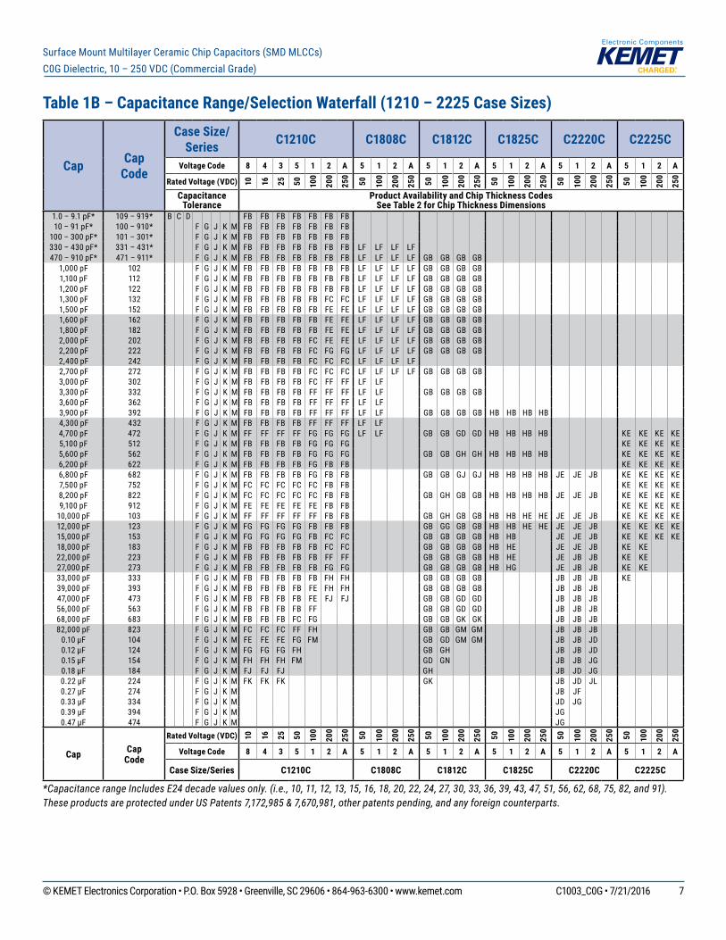
1.0–9.1pF* 109–919* B C D FB FB FB FB FB FB FB10–91pF* 100–910* F G J K M FB FB FB FB FB FB FB
100–300pF* 101–301* F G J K M FB FB FB FB FB FB FB330–430pF* 331–431* F G J K M FB FB FB FB FB FB FB LF LF LF LF470–910pF* 471–911* F G J K M FB FB FB FB FB FB FB LF LF LF LF GB GB GB GB
1,000pF 102 F G J K M FB FB FB FB FB FB FB LF LF LF LF GB GB GB GB1,100pF 112 F G J K M FB FB FB FB FB FB FB LF LF LF LF GB GB GB GB1,200pF 122 F G J K M FB FB FB FB FB FB FB LF LF LF LF GB GB GB GB1,300pF 132 F G J K M FB FB FB FB FB FC FC LF LF LF LF GB GB GB GB1,500pF 152 F G J K M FB FB FB FB FB FE FE LF LF LF LF GB GB GB GB1,600pF 162 F G J K M FB FB FB FB FB FE FE LF LF LF LF GB GB GB GB1,800pF 182 F G J K M FB FB FB FB FB FE FE LF LF LF LF GB GB GB GB2,000pF 202 F G J K M FB FB FB FB FC FE FE LF LF LF LF GB GB GB GB2,200pF 222 F G J K M FB FB FB FB FC FG FG LF LF LF LF GB GB GB GB2,400pF 242 F G J K M FB FB FB FB FC FC FC LF LF LF LF2,700pF 272 F G J K M FB FB FB FB FC FC FC LF LF LF LF GB GB GB GB3,000pF 302 F G J K M FB FB FB FB FC FF FF LF LF3,300pF 332 F G J K M FB FB FB FB FF FF FF LF LF GB GB GB GB3,600pF 362 F G J K M FB FB FB FB FF FF FF LF LF3,900pF 392 F G J K M FB FB FB FB FF FF FF LF LF GB GB GB GB HB HB HB HB4,300pF 432 F G J K M FB FB FB FB FF FF FF LF LF4,700pF 472 F G J K M FF FF FF FF FG FG FG LF LF GB GB GD GD HB HB HB HB KE KE KE KE5,100pF 512 F G J K M FB FB FB FB FG FG FG KE KE KE KE5,600pF 562 F G J K M FB FB FB FB FG FG FG GB GB GH GH HB HB HB HB KE KE KE KE6,200pF 622 F G J K M FB FB FB FB FG FB FB KE KE KE KE6,800pF 682 F G J K M FB FB FB FB FG FB FB GB GB GJ GJ HB HB HB HB JE JE JB KE KE KE KE7,500pF 752 F G J K M FC FC FC FC FC FB FB KE KE KE KE8,200pF 822 F G J K M FC FC FC FC FC FB FB GB GH GB GB HB HB HB HB JE JE JB KE KE KE KE9,100pF 912 F G J K M FE FE FE FE FE FB FB KE KE KE KE10,000pF 103 F G J K M FF FF FF FF FF FB FB GB GH GB GB HB HB HE HE JE JE JB KE KE KE KE12,000pF 123 F G J K M FG FG FG FG FB FB FB GB GG GB GB HB HB HE HE JE JE JB KE KE KE KE15,000pF 153 F G J K M FG FG FG FG FB FC FC GB GB GB GB HB HB JE JE JB KE KE KE KE18,000pF 183 F G J K M FB FB FB FB FB FC FC GB GB GB GB HB HE JE JE JB KE KE22,000pF 223 F G J K M FB FB FB FB FB FF FF GB GB GB GB HB HE JE JB JB KE KE27,000pF 273 F G J K M FB FB FB FB FB FG FG GB GB GB GB HB HG JE JB JB KE KE33,000pF 333 F G J K M FB FB FB FB FB FH FH GB GB GB GB JB JB JB KE39,000pF 393 F G J K M FB FB FB FB FE FH FH GB GB GB GB JB JB JB47,000pF 473 F G J K M FB FB FB FB FE FJ FJ GB GB GD GD JB JB JB56,000pF 563 F G J K M FB FB FB FB FF GB GB GD GD JB JB JB68,000pF 683 F G J K M FB FB FB FC FG GB GB GK GK JB JB JB82,000pF 823 F G J K M FC FC FC FF FH GB GB GM GM JB JB JB0.10µF 104 F G J K M FE FE FE FG FM GB GD GM GM JB JB JD0.12µF 124 F G J K M FG FG FG FH GB GH JB JB JD0.15µF 154 F G J K M FH FH FH FM GD GN JB JB JG0.18µF 184 F G J K M FJ FJ FJ GH JB JD JG0.22µF 224 F G J K M FK FK FK GK JB JD JL0.27µF 274 F G J K M JB JF0.33µF 334 F G J K M JD JG0.39µF 394 F G J K M JG0.47µF 474 F G J K M JG
Cap Cap Code
Rated Voltage (VDC) 10 16 25 50 100
200
250
50 100
200
250
50 100
200
250
50 100
200
250
50 100
200
250
50 100
200
250
Voltage Code 8 4 3 5 1 2 A 5 1 2 A 5 1 2 A 5 1 2 A 5 1 2 A 5 1 2 A
Case Size/Series C1210C C1808C C1812C C1825C C2220C C2225C
Package quantity based on finished chip thickness specifications.1 If ordering using the 2 mm Tape and Reel pitch option, the packaging quantity outlined in the table above will be doubled. This option is limited to EIA
0603 (1608 metric) case size devices. For more information regarding 2 mm pitch option see “Tape & Reel Packaging Information”.
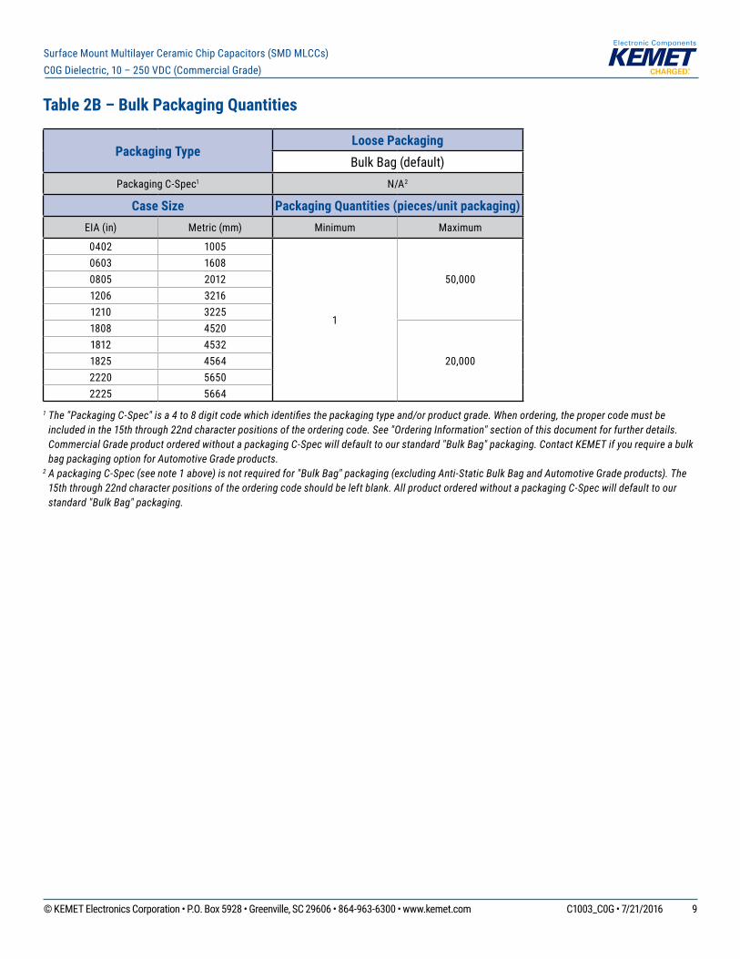
1 The "Packaging C-Spec" is a 4 to 8 digit code which identifies the packaging type and/or product grade. When ordering, the proper code must be included in the 15th through 22nd character positions of the ordering code. See "Ordering Information" section of this document for further details. Commercial Grade product ordered without a packaging C-Spec will default to our standard "Bulk Bag" packaging. Contact KEMET if you require a bulk bag packaging option for Automotive Grade products.
2 A packaging C-Spec (see note 1 above) is not required for "Bulk Bag" packaging (excluding Anti-Static Bulk Bag and Automotive Grade products). The 15th through 22nd character positions of the ordering code should be left blank. All product ordered without a packaging C-Spec will default to our standard "Bulk Bag" packaging.
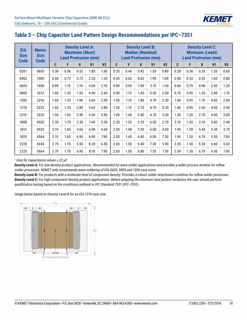
1 Only for capacitance values ≥ 22 µFDensity Level A: For low-density product applications. Recommended for wave solder applications and provides a wider process window for reflow solder processes. KEMET only recommends wave soldering of EIA 0603, 0805 and 1206 case sizes.Density Level B: For products with a moderate level of component density. Provides a robust solder attachment condition for reflow solder processes.Density Level C: For high component density product applications. Before adapting the minimum land pattern variations the user should perform qualification testing based on the conditions outlined in IPC Standard 7351 (IPC–7351).
Image below based on Density Level B for an EIA 1210 case size.
* 2 mm pitch reel only available for 0603 EIA case size. 2 mm pitch reel for 0805 EIA case size under development.
Benefi ts of Changing from 4 mm to 2 mm Pitching Spacing• Lower placement costs• Doublethepartsoneachreelresultsinfewerreelchangesandincreasedefficiency
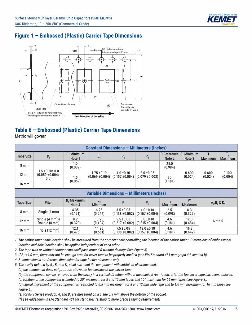
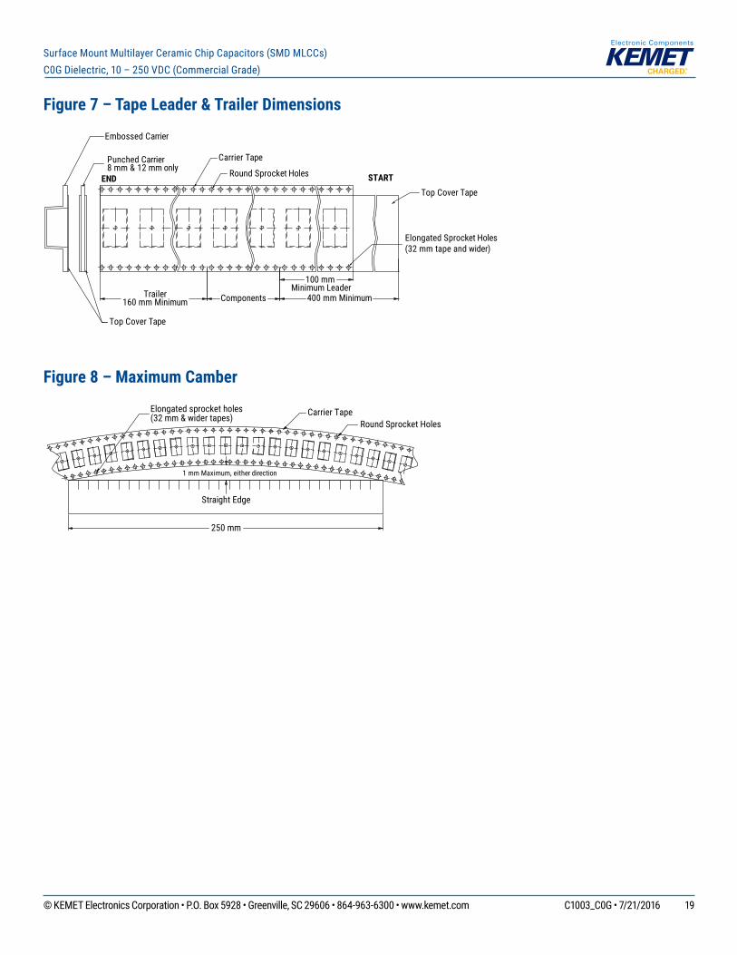
1. The embossment hole location shall be measured from the sprocket hole controlling the location of the embossment. Dimensions of embossment location and hole location shall be applied independent of each other.
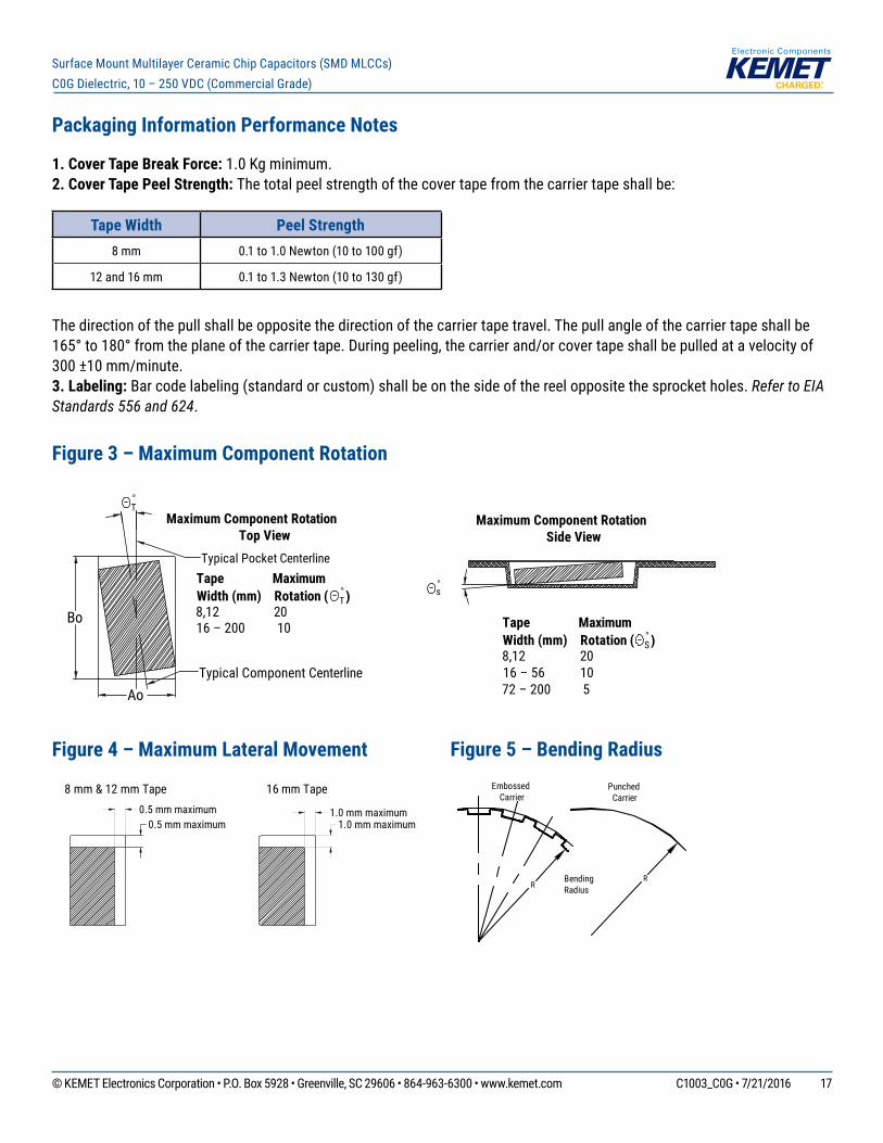
2. The tape with or without components shall pass around R without damage (see Figure 6).3. If S1 < 1.0 mm, there may not be enough area for cover tape to be properly applied (see EIA Standard 481 paragraph 4.3 section b).4. B1 dimension is a reference dimension for tape feeder clearance only.5. The cavity defi ned by A0, B0 and K0 shall surround the component with suffi cient clearance that: (a) the component does not protrude above the top surface of the carrier tape. (b) the component can be removed from the cavity in a vertical direction without mechanical restriction, after the top cover tape has been removed. (c) rotation of the component is limited to 20° maximum for 8 and 12 mm tapes and 10° maximum for 16 mm tapes (see Figure 3). (d) lateral movement of the component is restricted to 0.5 mm maximum for 8 and 12 mm wide tape and to 1.0 mm maximum for 16 mm tape (see
Figure 4). (e) for KPS Series product, A0 and B0 are measured on a plane 0.3 mm above the bottom of the pocket. (f) see Addendum in EIA Standard 481 for standards relating to more precise taping requirements.
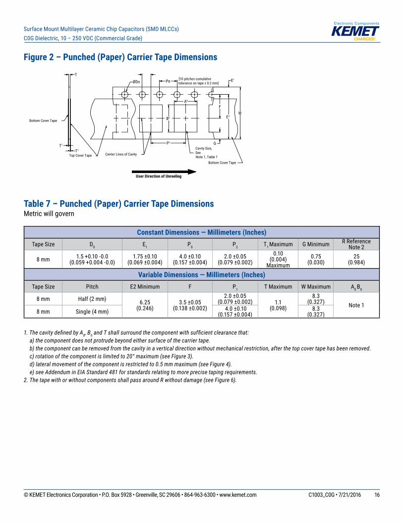
1. The cavity defi ned by A0, B0 and T shall surround the component with suffi cient clearance that: a) the component does not protrude beyond either surface of the carrier tape. b) the component can be removed from the cavity in a vertical direction without mechanical restriction, after the top cover tape has been removed. c) rotation of the component is limited to 20° maximum (see Figure 3). d) lateral movement of the component is restricted to 0.5 mm maximum (see Figure 4). e) see Addendum in EIA Standard 481 for standards relating to more precise taping requirements.2. The tape with or without components shall pass around R without damage (see Figure 6).
Tape Width Peel Strength8 mm 0.1to1.0Newton(10to100gf)
12 and 16 mm 0.1to1.3Newton(10to130gf)
Thedirectionofthepullshallbeoppositethedirectionofthecarriertapetravel.Thepullangleofthecarriertapeshallbe165°to180°fromtheplaneofthecarriertape.Duringpeeling,thecarrierand/orcovertapeshallbepulledatavelocityof300±10mm/minute.3. Labeling:Barcodelabeling(standardorcustom)shallbeonthesideofthereeloppositethesprocketholes.Refer to EIA Standards 556 and 624.