Page 1
SANDIA REPORT SAND2012-1292 Unlimited Release March 2012
Surface Photovoltage Measurements
and Finite Element Modeling of SAW
Devices Christine Donnelly
Prepared by Sandia National Laboratories Albuquerque, New Mexico 87185 and Livermore, California 94550
Sandia National Laboratories is a multi-program laboratory managed and operated by Sandia Corporation, a wholly owned subsidiary of Lockheed Martin Corporation, for the U.S. Department of Energy's National Nuclear Security Administration under contract DE-AC04-94AL85000. Approved for public release; further dissemination unlimited.
Page 2
2
Issued by Sandia National Laboratories, operated for the United States Department of Energy
by Sandia Corporation.
NOTICE: This report was prepared as an account of work sponsored by an agency of the
United States Government. Neither the United States Government, nor any agency thereof,
nor any of their employees, nor any of their contractors, subcontractors, or their employees,
make any warranty, express or implied, or assume any legal liability or responsibility for the
accuracy, completeness, or usefulness of any information, apparatus, product, or process
disclosed, or represent that its use would not infringe privately owned rights. Reference herein
to any specific commercial product, process, or service by trade name, trademark,
manufacturer, or otherwise, does not necessarily constitute or imply its endorsement,
recommendation, or favoring by the United States Government, any agency thereof, or any of
their contractors or subcontractors. The views and opinions expressed herein do not
necessarily state or reflect those of the United States Government, any agency thereof, or any
of their contractors.
Printed in the United States of America. This report has been reproduced directly from the best
available copy.
Available to DOE and DOE contractors from
U.S. Department of Energy
Office of Scientific and Technical Information
P.O. Box 62
Oak Ridge, TN 37831
Telephone: (865) 576-8401
Facsimile: (865) 576-5728
E-Mail: [email protected]
Online ordering: http://www.osti.gov/bridge
Available to the public from
U.S. Department of Commerce
National Technical Information Service
5285 Port Royal Rd.
Springfield, VA 22161
Telephone: (800) 553-6847
Facsimile: (703) 605-6900
E-Mail: [email protected]
Online order: http://www.ntis.gov/help/ordermethods.asp?loc=7-4-0#online
Page 3
3
SAND2012-1292
Unlimited Release
March 2012
Surface Photovoltage Measurements and Finite
Element Modeling of SAW Devices
Christine Donnelly
1749
Sandia National Laboratories
P.O. Box 5800
Albuquerque, New Mexico 87185-MS1080
Abstract
Over the course of a Summer 2011 internship with the MEMS department of Sandia National
Laboratories, work was completed on two major projects. The first and main project of the summer
involved taking surface photovoltage measurements for silicon samples, and using these
measurements to determine surface recombination velocities and minority carrier diffusion lengths
of the materials. The SPV method was used to fill gaps in the knowledge of material parameters
that had not been determined successfully by other characterization methods.
The second project involved creating a 2D finite element model of a surface acoustic wave device.
A basic form of the model with the expected impedance response curve was completed, and the
model is ready to be further developed for analysis of MEMS photonic resonator devices.
Page 5
5
Table of Contents Sect 1: Surface Photovoltage Measurements ........................................................................................
Introduction/Background.......................................................................................................................... 7
Applications ............................................................................................................................................. 10
Materials and Methods ........................................................................................................................... 10
Measurement Techniques ...................................................................................................................... 11
Results ..................................................................................................................................................... 12
Discussion and Future Steps ................................................................................................................... 14
Sect 2: COMSOL Modeling of Surface Acoustic Wave Resonators ...........................................................
Background and Motivation ................................................................................................................... 15
Initial Modeling ....................................................................................................................................... 18
References ....................................................................................................................................... 22
Appendix A1: Additional Figures and Data ............................................................................................... 23
Appendix B: MATLAB Code ........................................................................................................................ 24
FIGURES ..........................................................................................................................................................
Figure 1: Illuminated P-type wafer ........................................................................................................... 9
Figure 2: Light Bandwidth vs. Monochromator Slit Width ..................................................................... 11
Figure 3: Goodman Plot for silicon samples ........................................................................................... 13
Figure 4: Surface recombination velocities and minority carrier diffusion lengths for silicon samples . 13
Figure 5: Typical two-port resonator SAW device .................................................................................. 16
Figure 6: Impedance vs frequency for 1D COMSOL model ..................................................................... 19
Figure 7: COMSOL model of one-port SAW device ................................................................................. 19
Figure 8: Impedance response curve for modeled SAW device ............................................................ 20
Figure 9: Wave amplitude in solution to modeled SAW device ............................................................. 21
Figure 10: Reflectivities of silicon samples ............................................................................................. 23
Figure 11:Parameters for silicon samples determined by SPV measurements……………………………………23
Page 7
7
Section 1: Surface Photovoltage Measurements
Introduction
The surface photovoltage (SPV) technique is a contactless method for measuring properties of
semiconductor wafers without causing damage to the samples. It is often used to measure the
quality of samples, and to determine material parameters. The technique consists of shining
monochromatic light on a sample wafer, and measuring the resulting change in surface potential
with a lock-in amplifier.
The SPV measurement technique was used to determine surface recombination velocities and
minority carrier diffusion lengths of silicon samples that were fabricated using a variety of
passivation methods. This data was used to supplement measurements taken using the
photoconductance decay method.
Background:
Theory:
At the surface of a semiconductor material, dangling bonds create energy states that do not exist in
the bulk material. These states serve as a trap for charge carriers, and cause there to be a net
positive charge at the surface if the semiconductor is a p-type material. This nonzero charge
distribution causes an electric field to exist at the material’s surface, which sweeps free charge
carriers out of a region near the surface known as the space-charge region.
When the material is illuminated by photons that are above the bandgap energy, electron-hole pairs
are created and additional carriers will be swept either away from or toward the surface, causing
the surface voltage to change. For p-type semiconductors, electrons are brought to the surface and
holes move away from the surface. The change in surface voltage is measured in the SPV process.
Only those generated charge carriers that reach the space-charge region before recombining with a
charge carrier of the opposite type will contribute to a change in the surface voltage. Therefore, the
measurement provides a means of determining the distance that charge carriers diffuse through
the material before recombining: the minority carrier diffusion length.
Page 8
8
The minority carrier diffusion length is an important parameter for devices such as solar cells that
rely on diffusion of charge carriers across a depletion region. In addition, the diffusion length can
be used to measure defect densities in semiconductor materials. The minority carrier diffusion
length can be expected to decrease when defect densities increase.
Surface recombination velocity is an additional important parameter for prediction of device
performance. For devices such as solar cells, a high SRV is undesirable because this means that
charge carriers are moving to the surface of the material and not contributing to current through
the load.
The analysis of the surface photovoltage begins with the continuity equation for a semiconductor in
stready-state:
where D is the diffusion coefficient, G is the generation and is the minority carrier lifetime.
At the top surface of the material, a boundary condition for this equation is:
Where s1 has units of velocity and is known as the surface recombination velocity.
At the bottom surface of the material, the boundary condition can be written:
Finally, when there is light incident on the sample, the generation is given by
λ) = Io(λ)α(λ)(1-R)*exp(-αx),
where R is the reflectivity, α is the wavelength-dependent absorption coefficient and Io is the
incident photon flux (photon/(sec•cm2)).
Page 9
9
Figure 1: Illuminated P-type wafer
The solution to the continuity equation, given these boundary conditions, is a complex expression
with hyperbolic sine and cosine terms. However, the result can be simplified substantially when
the following assumptions are made:
1) Space-charge region width is much smaller than wafer thickness.
2) Wafer is much thicker than minority carrier diffusion length
3) Back contact has high surface recombination, so that s2 becomes infinitely large.
After making these assumptions, the equation for excess carrier concentration at the space-charge
region boundary becomes:
Assuming that the surface photovoltage is directly proportional to the excess carrier concentration
at the edge of the space-charge region, (the “Law of Junction” for eV>>kT), the
equation can be rewritten:
Page 10
10
When the equation is written in this form, it is apparent that plotting (1/V) vs. (1/α), both of which
are wavelength-dependent properties, will yield a line with an x-intercept of –Ln. A graph in this
form is known as a Goodman Plot.
Applications:
The main experimental objective was to characterize a variety of silicon samples intended for solar
cell applications. These samples were created using a range of fabrication and surface passivation
methods. The samples included both Czochralski and float zone wafers that either had no oxide
layer, or a 20 nm layer produced by either the wet or dry deposition method. Some of the samples
also had a 60 nm nitride layer deposited either by plasma enhanced chemical vapor deposition
(PECVD) or low pressure chemical vapor deposition (LPCVD). PECVD, which tends to cause surface
passivation by creating a positively charged layer at the surface of the sample, is currently the
preferred passivation method for solar cells. The LPCVD method mainly causes surface passivation
by filling dangling bonds and is not generally used for solar cell applications. However, LPCVD has
the advantage that it can be used to fully coat all surfaces of a sample with nitride, rather than only
the top exposed surface.
Because the samples were intended for an application that requires LPCVD coating, one goal of the
measurements was to determine whether samples that used the LPCVD nitride deposition process
could achieve reasonably low surface recombination velocities and high minority carrier diffusion
lengths. The more general goal was to determine optimal surface passivation methods for solar
cells.
Materials and Methods
Experimental Setup:
A monochromator containing a diffraction grating was used to filter input light from a lamp, and
produce output light over a narrow wavelength range. The light source was chopped at
approximately 150 Hz using an optical chopper, and light traveled via a fiber-optic cable to the
sample. The sample was illuminated and the resulting change in surface voltage was measured with
a lock-in amplifier using capacitive coupling techniques.
Page 11
11
Through LabView interfacing with the monochromator and lock-in amplifier, a wavelength sweep
was taken and the resulting change in voltage was measured at each wavelength. The measurement
time constant was one second, and 3 measurements were averaged per wavelength step.
Measurement Techniques:
Narrowing light bandwidth:
While the monochromator would ideally produce light at a single wavelength, in reality the light
output contains a range of wavelengths. The light from a lamp is separated by the instrument’s
diffraction grating, and the angle of an internal mirror determines which of the diffracted
wavelengths leave through the instrument’s output slit. Therefore, the wider the slit width, the
larger the output bandwidth. A variety of slit widths were tried in order to find a balance between
eliminating light noise and obtaining a detectable signal. The bandwidth was eventually reduced to
under 20 nm with a 30 micrometer slit width. At lower slit widths, the intensity of incident light on
the sample was too low to yield a measureable change in surface voltage.
Figure 2: Light Bandwidth vs. Monochromator Slit Width
Monochromator calibration:
A thorough calibration of the monochromator was performed. Because the absorption coefficient is
highly wavelength-dependent in the range of wavelengths being used, even small calibration errors
are undesirable.
Page 12
12
Multiple steps were taken to ensure accurate calibration. A ThorLabs spectrometer measured light
output from four different spectral calibration lamps (Hg, Xe, Ar, and Kr). By comparing multiple
spectral lines that occur at known wavelengths with the measured spectrometer value, the
spectrometer calibration offset was determined. The spectrometer could then be accurately used
to test the monochromator output wavelength, and to recalibrate the monochromator.
The calibration accuracy was independently double-checked by using light filters for which there
exist published intensity-vs.-wavelength curves. Intensity sweeps were taken with the
monochromator while a filter was in place, and the measured intensity-wavelength curves were
compared to the published plots.
Photon flux normalization:
The photon flux must be known in order to use Goodman plots and accurately calculate the
minority carrier diffusion length of the samples. To determine photon flux, the fiber-optic cable
output was measured with a photodetector immediately following each SPV measurement sweep.
The photodetector current and its known responsivity-vs.-wavelength curve (amps/watt) was used
to determine power, as well as photon flux.
Surface reflectivity:
The surface reflectivity was measured using a spectrophotometer. Light was shined onto the
sample with a monochromator, and the amount of reflected vs. absorbed light was measured.
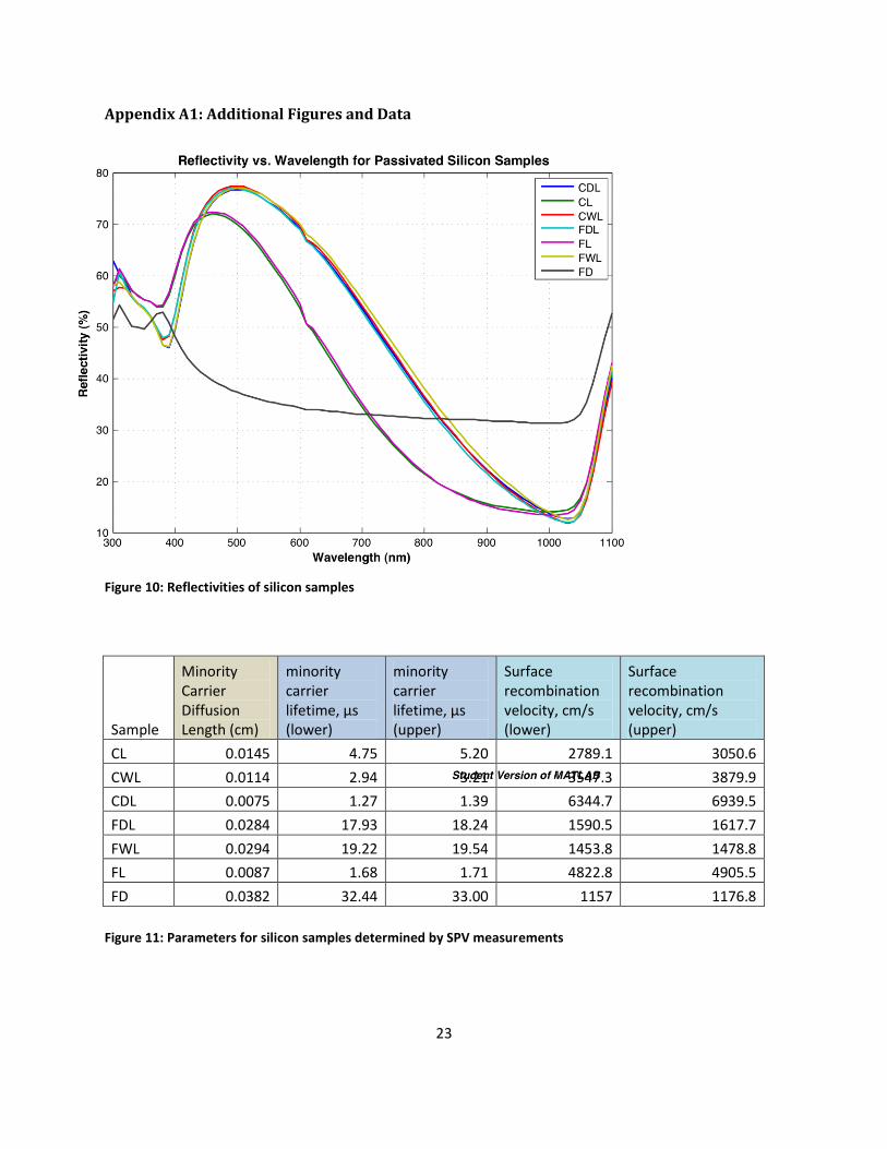
Reflectivity data for the seven silicon samples measured is shown in Appendix A.
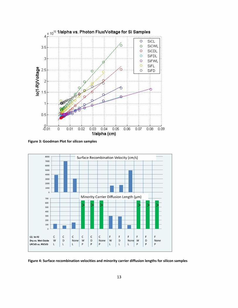
Results:
An SPV signal could be detected for seven of the silicon samples. The Goodman Plot for these
samples is shown in Figure 3. The samples that were coated with a nitride layer using the PECVD
deposition technique did not produce a measureable SPV signal, due to the fact that their minority
carrier diffusion lengths were greater than the sample thickness (650 um), which violates one of
the assumptions used when relating surface photovoltage to minority carrier diffusion length.
Values for minority carrier diffusion length and lifetime, as well as surface recombination velocities,
are shown in table format in Appendix A.
Page 13
13
Figure 3: Goodman Plot for silicon samples
Figure 4: Surface recombination velocities and minority carrier diffusion lengths for silicon samples
Page 14
14
Discussion and Future Steps:
Using the surface photovoltage technique, multiple samples that could not be measured using the
photoconductance decay method due to their relatively low diffusion lengths were able to be
characterized. An additional variable which must be explored before passivation techniques can be
directly compared is the contamination levels of the equipment in the fabrication facilities. Samples
that have been fabricated using equipment with higher contamination levels will see a decrease in
minority carrier diffusion length that is not due solely to the intrinsic quality of the passivation
method. Therefore, the results can only be used to compare the efficacy of passivation techniques
that take place using the Sandia fabrication facilities, and cannot yet be extended to make general
conclusions about optimal surface passivation methods.
In order to separate the effectiveness of a passivation method from the contamination levels of
equipment, an additional set of experiments must be performed in which minority carrier diffusion
lengths are measured before and after the use of fab equipment for each individual process. In
order to take these measurements, the amount of noise contamination in the experimental setup
must be decreased so that a signal can be measured for bare silicon samples, which will have higher
recombination velocities, low diffusion lengths and low overall changes in surface voltage with
photonic excitement.
Page 15
15
Sect 2: COMSOL Modeling of Surface Acoustic Wave Resonators
Background and Motivation:
The purpose of this project was to produce a basic 2-D finite element model of a surface acoustic
wave (SAW) device, and then to expand this model to account for varying device geometries and
materials. The FEM model will eventually be used to analyze MEMS photonic resonator devices
that function similarly to SAW devices and are being developed at Sandia .
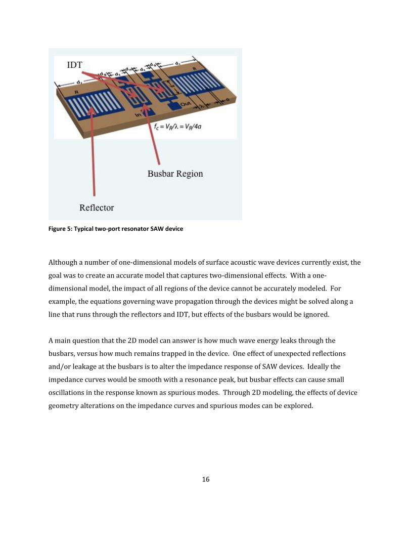
SAWs are waves that are generated at the free surface of an elastic solid. In a typical two-port
surface acoustic wave device, there are two IDTs (interdigital transducers) which consist of metal
fingers deposited on a piezoelectric material that are connected to either a ground or signal busbar.
One of the IDTs serves to convert an alternating voltage on the busbars into mechanical waves in
the piezoelectric material. Reflectors that surround the IDTs consist of grounded metal fingers with
the same spacing as the IDT fingers, and these serve to trap acoustic energy within the device. The
other IDT then converts the vibrations into an output signal. A two-port resonator device is shown
in Figure 5.
SAW and photonic resonator devices can act as filters and have applications for a variety of
technologies, such as cell phones. The metal fingers for the IDTs are spaced at some design
resonance frequency. When the input signal is at the resonance frequency, standing waves will be
produced in the IDT region and the device will have low impedance, producing a high output
current. At other frequencies, this phenomenon will not occur, and the current response of the
device will be low.
Page 16
16
Figure 5: Typical two-port resonator SAW device
Although a number of one-dimensional models of surface acoustic wave devices currently exist, the
goal was to create an accurate model that captures two-dimensional effects. With a one-
dimensional model, the impact of all regions of the device cannot be accurately modeled. For
example, the equations governing wave propagation through the devices might be solved along a
line that runs through the reflectors and IDT, but effects of the busbars would be ignored.
A main question that the 2D model can answer is how much wave energy leaks through the
busbars, versus how much remains trapped in the device. One effect of unexpected reflections
and/or leakage at the busbars is to alter the impedance response of SAW devices. Ideally the
impedance curves would be smooth with a resonance peak, but busbar effects can cause small
oscillations in the response known as spurious modes. Through 2D modeling, the effects of device
geometry alterations on the impedance curves and spurious modes can be explored.
Page 17
17
One method commonly used to analyze wave propagation in SAW devices is the Coupling of Modes
technique. A general idea of the derivation of the one-dimensional COM equations is described
below:
Initially, a wave is written as a field φ(x). Using the loaded wave equation, the field can be written
The field can also be written as φ(x)=exp(-iβx)*Φ(x), where Φ(x) is periodic with period p and β is
a wavenumber. By design, the spacing of the IDT fingers will be such that they have a half-period s,
corresponding to a total period of 2s and a wavenumber βIDT = (pi/s). This characteristic
wavenumber which is meant to match the resonance wavenumber of excitations to the device.
Therefore, at design conditions, βinput = n*pi/s. Using the COM technique, the input wavenumber is
assumed to be βinput = n*pi/s + q, where q is a small deviation from the resonance wavenumber.
Because Φ(x) is periodic with period p, it has a Fourier series and can be written in terms of a sum
of harmonic wavenumbers,
The field φ(x) can therefore also be written in terms of a sum of complex exponentials with
wavenumbers
n 2n
p , or in the case of input waves for a SAW device near resonance
frequency,
n qn
s . Taking only the harmonics n=1 and n=-1, the total expression then
becomes .
If the terms are substituted into the loaded wave equation, under a number of simplifying
assumptions, terms can be recombined to form the following set of equations for the IDT region of
the device:
Page 18
18
Using a two-dimensional loaded wave equation and adding in a periodic voltage forcing with
amplitude V, the equations describing the movement of waves through a SAW device become:
In the reflector region of the device, where there are fingers at half-period spacing s but no applied
voltage, the equations become:
In the busbar region of the device, where no fingers exist and there are no internal reflections, the
equations become:
Initial Modeling
One-Dimensional Model
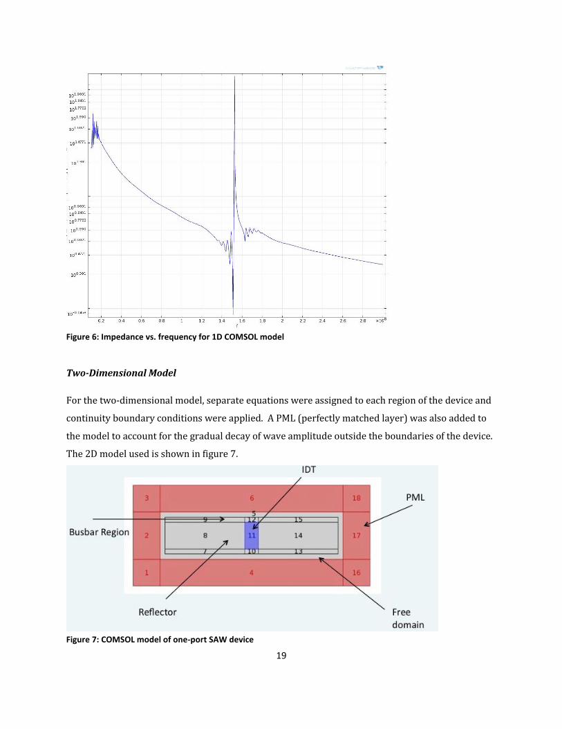
A model of the SAW devices was created using COMSOL, a finite element modeling program. The
one-dimensional COM equations were initially solved to ensure modeling accuracy. Results of this
model, which displayed the expected resonance behavior, are shown in Figure 6.
Page 19
19
Figure 6: Impedance vs. frequency for 1D COMSOL model
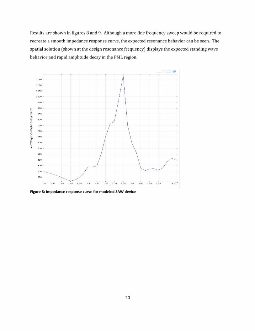
Two-Dimensional Model
For the two-dimensional model, separate equations were assigned to each region of the device and
continuity boundary conditions were applied. A PML (perfectly matched layer) was also added to
the model to account for the gradual decay of wave amplitude outside the boundaries of the device.
The 2D model used is shown in figure 7.
Figure 7: COMSOL model of one-port SAW device
Page 20
20
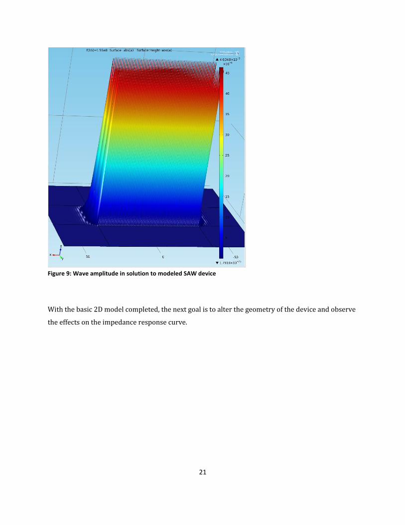
Results are shown in figures 8 and 9. Although a more fine frequency sweep would be required to
recreate a smooth impedance response curve, the expected resonance behavior can be seen. The
spatial solution (shown at the design resonance frequency) displays the expected standing wave
behavior and rapid amplitude decay in the PML region.
Figure 8: Impedance response curve for modeled SAW device
Page 21
21
Figure 9: Wave amplitude in solution to modeled SAW device
With the basic 2D model completed, the next goal is to alter the geometry of the device and observe
the effects on the impedance response curve.
Page 22
22
References
Plesky, Victor and Julius Koskela. “Coupling-of-Modes Analysis of SAW Devices.” International
Jounral of High Speed Electronics and Systems (2000): 867-947.
Schroder, Dieter K. “Surface Voltage and Surface Photovoltage: History, Theory, and Applications.”
Measurement Science and Technology (2001): 16-31.
Tokuda, Osamu and Kazuhiro Hirota. “Two-Dimensional Coupling-of-Modes Analysis in Surface
Acoustic Wave Devic e Performed by COMSOL Multiphysics.” Japanese Journal of Applied Physics
(2011): 1-4.
Page 23
23
Appendix A1: Additional Figures and Data
Figure 10: Reflectivities of silicon samples
Sample
Minority Carrier Diffusion Length (cm)
minority carrier lifetime, μs (lower)
minority carrier lifetime, μs (upper)
Surface recombination velocity, cm/s (lower)
Surface recombination velocity, cm/s (upper)
CL 0.0145 4.75 5.20 2789.1 3050.6
CWL 0.0114 2.94 3.21 3547.3 3879.9
CDL 0.0075 1.27 1.39 6344.7 6939.5
FDL 0.0284 17.93 18.24 1590.5 1617.7
FWL 0.0294 19.22 19.54 1453.8 1478.8
FL 0.0087 1.68 1.71 4822.8 4905.5
FD 0.0382 32.44 33.00 1157 1176.8
Figure 11: Parameters for silicon samples determined by SPV measurements
Page 24
24
Appendix B: MATLAB Code
Surface Photovoltage Post-Processing:
function [Ln, srv_est_avg] = spvdata_Si2()
% function written specifically for passivated silicon samples
global direc;
direc = '\\snl\mesa\Users\cdonnel\Summer2011SPVMeasurements\';
cd([direc 'Text File Outputs']);
fprintf('\n Type "y" or "Y" for yes. \n\n');
%% Constants
T = 293; %temperature
e = 1.6E-19; %electron charge in coulombs
k = 1.38E-23; %Boltzmann's constant
ni = 1.5E10; %intrinsic carrier concentration for silicon, cm^-3, at T = 300
K
%% Initialize plots
figure;
ax1 = gca;
hold(ax1,'all');
figure;
ax2 = gca;
hold(ax2,'all');
%% Choose sample type and files to be used (here, file list is hardcoded)
sample = input('Sample Type? (Default Si) ','s');
if isempty(sample)
sample = 'Si';
end
if any(strcmpi(sample,{'GaAs';'GaAs/InGaP'}))
a = textread([direc 'Text File Outputs\GaAs_lambda_vs_alpha_10^-8.txt']);
lambda = a(:,1)*10^8;
alpha = a(:,2)*10^8;
else if any(strcmpi(sample,{'Si';'SiP';'Si-P';'SiN';'Si-N'}))
a = textread([direc 'Text File Outputs\SiAbsorption.txt']);
lambda = a(:,1);
alpha = a(:,2);
end
end
file =
Page 25
25
{'080511a_SiCL';'080511b_SiCWL';'080511a_SiCDL';'080511a_SiFDL';'080511a_SiFW
L';'080511a_SiFL';'080511a_SiFD'};
%%
for N = 1:length(file);
%%% Open next file and allow user to choose upper and lower wavelength
limit
%%%
%%%
fitlines = 0;
fprintf(['\n File: ' file{N} '\n']);
data = textread([direc 'Text File Outputs\' file{N}]);
[data] = normalize(data,file{N});
step = data(end,end);
lowerlim = input(['Lower Limit? >= ' num2str(data(end,1)) ', multiple of
' num2str(step) ' ']);
if isempty(lowerlim)
lowerlim = data(end,1);
end
upperlim = input(['Upper Limit? <= ' num2str(data(end,2)) ', multiple of
' num2str(step) ' ']);
if isempty(upperlim)
upperlim = data(end,2);
end
lowerind = find(data(:,1) >= lowerlim,1);
upperind = find(data(:,1) >= upperlim,1);
wincludes = data(lowerind:upperind,1); %wavelengths to include
vincludes = data(lowerind:upperind,2); %photovoltages to include
(normalized for photon flux)
%%% Interpolate to find best estimate for value of alpha
%%%
%%%
for m = 1:length(wincludes);
%a_inv(m) = 1/(lininterp(wincludes(m),lambda,alpha));
a_inv(m) = (84.732/(wincludes(m)*10^-3)-76.417)^-2;
v_inv(m) = 1/vincludes(m);
labels(m) = wincludes(m);
end
Page 26
26
goodinds = find(a_inv < inf); %may have gotten some that are in range
below bandgap energy and = 0
a_inv = a_inv(goodinds);
v_inv = v_inv(goodinds);
labels = labels(goodinds);
%%% Add lines and data labels to plots
%%%
%%%
h = plot(ax1,wincludes,vincludes,'linewidth',2);
col = get(h,'color');
g = plot(ax2,a_inv,v_inv,'o','color',col);
xlim = get(ax2,'XLim');
for m = 1:length(a_inv)
t(m) = text(a_inv(m)+.02*(xlim(2) -
xlim(1)),v_inv(m),num2str(labels(m)));
end
fitlines(1:length(a_inv),1:3) = [a_inv' v_inv' labels'];
%%% Give user the opportunity to exclude some data points from the
diffusion length fitline
if any(fitlines)
lowerfit = input('Lower Wavelength Limit for Fitline?');
if isempty(lowerfit)
lowerfit = min(fitlines(:,3));
end
upperfit = input('Upper Wavelength Limit for Fitlines?');
if isempty(upperfit)
upperfit = max(fitlines(:,3));
end
for m = 1:length(a_inv)
delete(t(m));
end
lowerind = find(fitlines(:,3) >= (lowerfit),1);
upperind = find(fitlines(:,3) >= (upperfit),1);
fitlines = fitlines(lowerind:upperind,:);
set(g,'xdata',fitlines(:,1));
set(g,'ydata',fitlines(:,2));
Page 27
27
a = polyfit(fitlines(:,1),fitlines(:,2),1);
alim = max(fitlines(:,1));
x = linspace(-1,alim,15000);
b = polyval(a,x);
Ln_ind = find(b > 0,1);
Ln(N) = x(Ln_ind);
slope(N) = a(1);
vtest(1:length(fitlines(:,2)),N) = 1./fitlines(:,2); %building a
matrix of 1/V values that were actually used in the fitline
%plot fitline
u = plot(ax2,x(find(x>0,1)-5:end),b(find(x>0,1)-5:end),'color',col);
axes(ax2);
set(get(get(u,'Annotation'),'LegendInformation'),...
'IconDisplayStyle','off'); % Exclude line from legend
end
end
figure;
hold all;
for n = 1:length(file)
name = file{n};
if strcmpi(name(11),'C')
Na = [8E15 8E14];
mu_n = [1.6E3 1.75E3];
else if strcmpi(name(11),'F')
mu_n = [1.75E3 1.78E3];
Na = [1.5E14 9E13];
end
end
zind = find(vtest(:,n) == 0,1); %some columns may have zeros since
certain fitlines contain more data than others
if isempty(zind) %case that data fills full column
zind = length(vtest(:,n));
end
for p = 1:zind - 1
for m = 1:2
no = (ni)^2/(Na(m));
Dn = (mu_n(m)*k*T)/e;
srv_est = (vtest(p,n)*e*no*(Ln(n)+a_inv(p)))/(Ln(n)*k*T) -
Page 28
28
(Dn/Ln(n));
srv_est_avg(n,m) = mean(srv_est);
end;
end;
end
leg = {'SiCL';'SiCWL';'SiCDL';'SiFDL';'SiFWL';'SiFL';'SiFD'};
%leg = {'SiCL3';'SiFD3';'SiFDL3';'SiFWL3'};%;'SiFWL';'SiFL';'SiFD'};
ylabel(ax1,'Voltage(V)','fontweight','bold','fontsize',12);
xlabel(ax1,'Wavelength(nm)','fontweight','bold','fontsize',12);
grid(ax1,'on');
title(ax1,['Wavelength vs. Surface Photovoltage for ' sample '
Samples'],'fontweight','bold','fontsize',12)
legend(ax1,leg);
ylabel(ax2,'Io(1-R)/Voltage','fontweight','bold','fontsize',12);
xlabel(ax2,'1/alpha (cm)','fontweight','bold','fontsize',12);
grid(ax2,'on');
title(ax2,['1/alpha vs. Io(1-R)/Voltage for ' sample '
Samples'],'fontweight','bold','fontsize',12);
legend(ax2, leg);
end
%%
function [outdata] = normalize(data,file) %[vincludes] =
filternorm(file,voltages,wavelengths)
h = 6.626E-34;
c = 2.998E8;
area = .5^2*pi; %cm^2
%%% Normalizes data for varying light intensities and amplifier gains
global direc;
wavelengths = data(:,1);
outdata = data;
[names,current,freq,filter,inslit,outslit,ligain,sensitivity,tc,ampgain,passb
and,recal,type] = textread([direc 'Excel
Workbooks\SummerSPVFiles.txt'],'%s%f%f%s%f%f%f%f%f%f%s%f%s%*[^\n]');
Page 29
29
ind = find(strcmp(names,file));
current = current(ind);
ligain = ligain(ind);
sens = sensitivity(ind)*10^-3;
ampgain = ampgain(ind);
filter = filter{ind};
ind2 = find(strcmp(names,filter));
filtersens = sensitivity(ind2)*10^-9;
if recal == 0
outdata(1:end,1) = outdata(1:end,1) - (900 - 883);
end
if ~strcmpi(filter,'none');
filterdata = textread([direc 'Text File Outputs\' filter]);
%Current vs. wavelength measured from photodiode for the specific filter used
in measurement
else
filterdata = textread([direc 'Text File Outputs\' NOFILTER
'.txt']); %should always use filter though
end
outdata(1:end - 1,2) = .5*sens*data(1:end - 1,2);
filterdata(1:end - 1,2) = .5*filtersens*filterdata(1:end - 1,2);
r = textread([direc 'Text File Outputs\Responsivity.txt']);
%responsivity (A/W)
reflectivity = textread([direc 'Excel
Workbooks\Reflectivity_from_Jose.txt']);
rheaders = textread([direc 'Excel
Workbooks\ReflectivityHeader.txt'],'%s');
for n = 1:length(wavelengths) - 1
fi = lininterp(wavelengths(n),filterdata(:,1),filterdata(:,2));
%measured photocurrent with filter in place
resp = lininterp(wavelengths(n),r(:,1),r(:,2)); %linear
interpolation to find responsivity
ind = find(strcmpi(file(11:end),rheaders));
refl =
.01*lininterp(wavelengths(n),reflectivity(:,1),reflectivity(:,ind+1));
e = h*c/(wavelengths(n)*10^-9); %energy per photon
photon = fi/(resp*e); %photon/sec
flux = photon/area; %photon/(sec*cm^2)
outdata(n,2) = data(n,2)/(flux*(1-refl)); %voltage normalized by
photon flux
end
Page 30
30
end
%%
function output = lininterp(val,tabvals,tabdata)
%%%% Function takes an arbitrary x value (val), and interpolates y
using a list
%%%% of tabulated x (tabvals) and y (tabdata) values and a linear
interpolation. If value of x falls below or above tabulated
%%%% list, output in "NaN"
ind = find(tabvals >= val,1);
if isempty(ind) || ind == 1
output = NaN;
else
dval = tabvals(ind) - tabvals(ind - 1); %width of gap of tabulated x values
in which the input x falls
dn = tabdata(ind) - tabdata(ind - 1); %width of gap of tabulated
y range
pct = (val - tabvals(ind - 1))/dval; %percent offset of input x
from lower limit
output = tabdata(ind - 1) + dn*pct;
end
end
Page 31
31
DISTRIBUTION
1 Christine Donnelly – 15 Central Street, Winchester MA 01890. [email protected]
(electronic copy)
1 MS0899 RIM-Reports Management 9532 (electronic copy)
1 MS1078 Wahid Hermina 1710 (electronic copy)
1 MS1080 Keith Ortiz 1749 (electronic copy)
1 MS1080 Jose Cruz-Campa 1749 (electronic copy)
1 MS1084 Darren Branch 1714 (electronic copy)
1 MS1085 Michael Cich 1742 (electronic copy)
1 MS1085 Charles Sullivan 1742 (electronic copy)
1 MS1085 Mike Baker 1742 (electronic copy)