Surface Studies of Niobium for Superconducting Radio Frequency (SRF) Cavities Hui Tian The Applied Science Department College of William and Mary This research was conducted at Thomas Jefferson National Accelerator Facility for the Department of Energy under grant DE-FG02-06ER41434 to the College of William and Mary
Transcript
Surface Studies of Niobium for Superconducting Radio Frequency (SRF) Cavities
Hui TianThe Applied Science Department
College of William and Mary
This research was conducted at Thomas Jefferson National Accelerator Facility for the
Department of Energy under grant DE-FG02-06ER41434 to the College of William and Mary
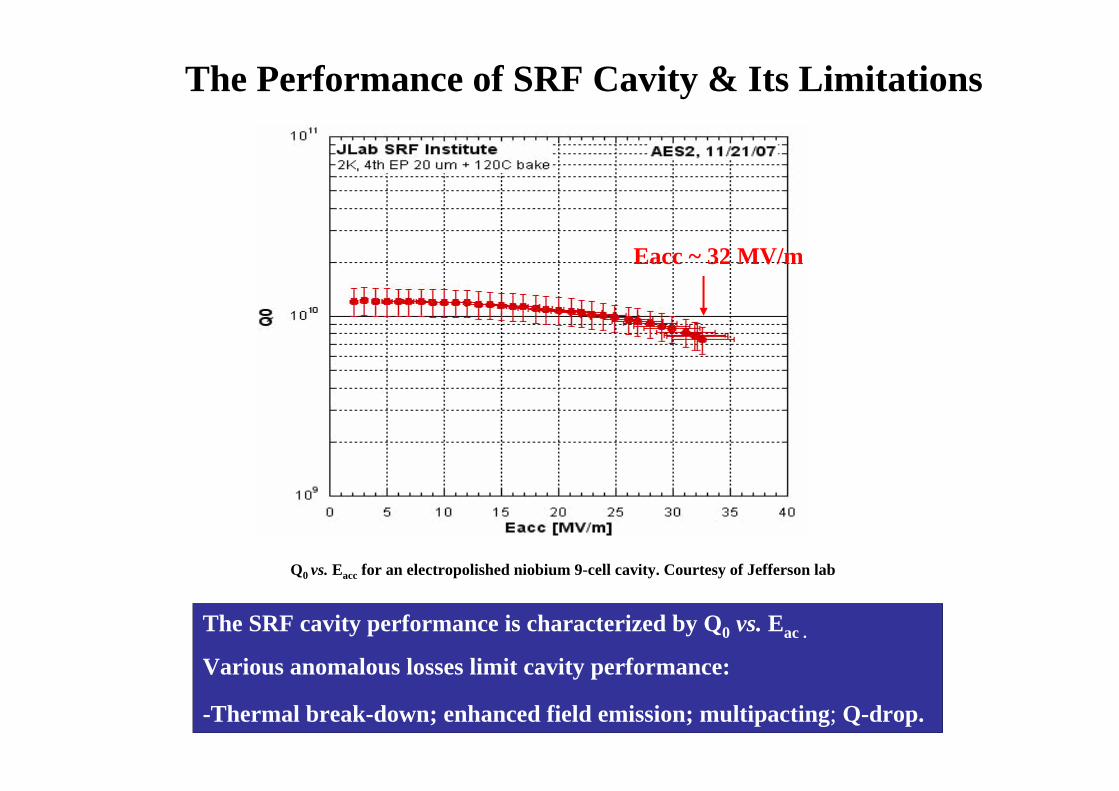
The Performance of SRF Cavity & Its Limitations
The SRF cavity performance is characterized by Q0 vs. Eac .
Various anomalous losses limit cavity performance:
-Thermal break-down; enhanced field emission; multipacting; Q-drop.
Q0 vs. Eacc for an electropolished niobium 9-cell cavity. Courtesy of Jefferson lab
Eacc ~ 32 MV/m
Current Nb SRF Cavity Surface Treatment Methods Needs Improvement
Cavities Processing Recipe (courtesy of www.linearcollider.org )1. Incoming cavity quality control checks.2. Optical inspection of as-received cavity.3.3. Bulk buffered chemical polishing( BCP)Bulk buffered chemical polishing( BCP)//electropolishingelectropolishing (EP)~(EP)~150 150
μμmm damage layer removal .damage layer removal .4. Ultrasonic degreasing.5. High-pressure rinsing.6. Hydrogen degassing at 600/800ºC.7. Field-flatness tuning.8.8. 20 20 μμm buffered chemical polishing( BCP)m buffered chemical polishing( BCP)//electropolishingelectropolishing (EP)(EP)9. Ultrasonic degreasing.10.Field-flatness verification and retuning if <95%.11.High-pressure rinsing.12.Assembly and vacuum leak testing.13.13.120120ººC bake.C bake.14.Vertical dewar test.
Current technology of cavities' surface treatment- “ a series of removal steps + low T baking ”- mechanical damage; chemical residues; hydrogen (bulk); particulate + oxygen, hydrogen, structure…
Undesirable surface effects including: magnetic field enhancement at a sharp transition, such as a grain boundary edge, the creation of anomalous “hot spots,” and electron multipacting.
Performance of Nb SRF Cavity Strongly
Impacted By Its Topmost Surface
Outline: Topography
1. Motivation-Understanding for Improving Performance.
2. Characterization of Niobium Surface Topography.
3. X-ray Photoelectron Spectroscopy (XPS) Studies of Niobium Surface Oxide.
4. Surface Study of Niobium Buffered Chemical Polished (BCP)Under Conditions for SRF Cavity Production.
5. Characterization of Niobium Electropolishing (EP).
Surface Topography Is a Critical Factor For Nb SRF Cavity
Magnetic field enhanced at the sharp protrusions. Courtesy from J. Knobloch et. al, the 9th SRF workshop in Santa Fe, NM.
Rz < 2 μm high gradient cavity ( > 30 MV/m). Courtesy from K. Satio, the 9th SRF workshop in Santa Fe, NM.
Both vertical & lateral surface topography information are important for Nb cavity
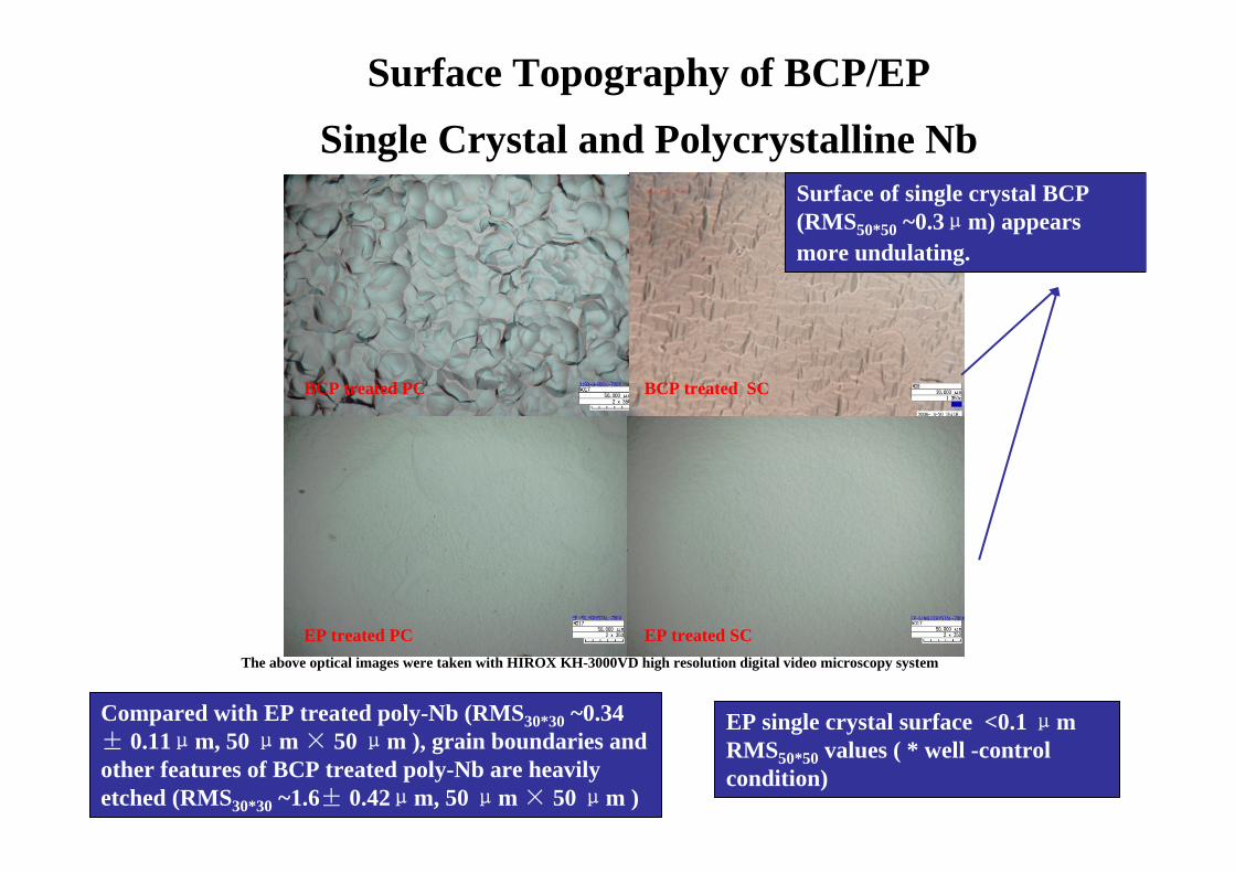
Surface Topography of BCP/EP Single Crystal and Polycrystalline Nb
The above optical images were taken with HIROX KH-3000VD high resolution digital video microscopy system
EP single crystal surface <0.1 μmRMS50*50 values ( * well -control condition)
BCP treated PC BCP treated SC
EP treated PC EP treated SC
Surface of single crystal BCP (RMS50*50 ~0.3μm) appears more undulating.
Compared with EP treated poly-Nb (RMS30*30 ~0.34 ± 0.11μm, 50 μm × 50 μm ), grain boundaries and other features of BCP treated poly-Nb are heavily etched (RMS30*30 ~1.6± 0.42μm, 50 μm × 50 μm )
RMS vs. Scan Area (µm * µm)
0
200
400
600
800
1000
1200
1400
1600
1800
2000
2200
2400
20 50 100 200 1000Scan Area ( µm * µm)
RM
S(nm
)
Ground+5 mins BCP
LightBCP( 20 mins BCP, ~ 30 µm removal)
HeavyBCP (90 mins BCP, ~ 150 µm removal)
Ground+30 mins EP ( 32 ± 1 º C)
RMS Roughness Alone Is Not Sufficient to Characterize Nb Surface Topography
Useful to get the average information about a surface variation .
No information about the lateral dimension of surface features.
RMS measurements are
scale dependent.
Profilometry
AFM
∑ −=ji
ji zzn
RMS,
2, )(1
Power Spectral Density (PSD) Provided a Promising Solution
Square of the Fourier transform of the surface height data; describes how the height varies according to spatial frequency; gives information regarding both lateral and vertical roughness.
Related to RMS roughness, autocorrelation length and fractal dimension.
Maximum and minimum frequencies in data are set by the Nyquist limits( ).⎥⎦
⎤⎢⎣⎡
∆∆ xxN 21,
21
2/ 2 / 22 ( )
2/ 2 / 2
1( , ) lim ( , ) x y
L Li f x f y
Lx yL L
PSD f f h x y e dxdyL
π− +∞
− −
= ∫ ∫uuur21
0( ) ( ) ( ) ( ) exp( 2 / ) ( )
N
x N nn
xPSD f m h x i nm N K mN
π−
=
∆= −∑
10-4
10-3
10-2
10-1
100
10110
0
102
104
106
108
1010
1012
Spatial Frequency ( µm -1)
PSD
(nm
2 )
PSD of Profilometry and AFM Data for Ground Sample with 5 Mins BCP
PSD Allows Integration of the Nb Surface Topographic
Measurements from AFM to Profilometry
The spatial frequency ranges corresponding to AFM & profilometry largely overlap; the different PSD functions agree with each other. A. Duparré, et. al., Appl. Opt. Vol. 41 (1), 2002
H. Tian, G. Ribeill, C. Reece, M. Kelley. Proceedings of 13th Workshop on RF Superconductivity
lateral scale of surface feature
Amplitude of surface height.
Profilometry :µm ~ mm
AFM: nm ~ µm
Surface Topography of Niobium Samples after BCP/EP Treatment
Ground light BCP( 20 mins) ~30μm
EP (30 mins)~15μm
Div: 6000 nm Div: 6000 nm
Div: 6000 nm Div: 3000 nm
EP has smaller PSD and the longest correlation length-better macro & micro polish.
Heavy BCP removes all mechanical damage, but results in a rougher surface.
The EBSD reveals the orientation of individual grains in the niobium surface; The information depth is about the same as the rf penetration depth, EBSD selectively views the material that matters.
The dominant grain orientation for BCP treated polycrystalline Nb is [100] .
Surface protrusions caused by mechanical grinding were quickly leveled out by a short period of EP, the edges of grain boundaries and recessed parts of surface were continually smoothed out by EP
Nb Surface Topographic Variation Under EP
Measured by Stylus profilometry
1000μm *1000μm
First quantitative characterization under controlled incremental EP
Summary and Future Work
The first use of power spectral density (PSD) in quantitatively characterizing the surface topography of niobium has been demonstrated. The effect of preparation variables on Nb surface topography has been studied systematically for the first time.
Longer BCP removes the mechanical damages but leaves a rougher surface. First quantitative characterization under controlled EP shows longer EP smoothes out the surface variations caused by different pre-treatments.
Future:
In parallel with EP study, a systematic Nb surface topography study is required for optimizing EP process.
Understand at what scales roughness is most important to cavity performance, then optimize process to those requirement.
Outline: XPS
1. Motivation-Understanding for Improving Performance.
2. Characterization of Niobium Surface Topography.
3. X-ray Photoelectron Spectroscopy (XPS) Studies of NiobiumSurface Oxide.
4. Surface Study of Niobium Buffered Chemical Polished (BCP)Under Conditions for SRF Cavity Production.
5. Characterization of Niobium Electropolishing (EP).
The surface chemistry of Nb is dominated by the high reactivity to oxygen; the outermost oxides layers are always found to be Nb2O5.
Suboxides in various combinations and morphologies are proposed to be between the Nb2O5 and the underlying metal.
Nb2O5
Nb
NbOx
Angle Resolved (AR) vs. Energy Resolved (ER)XPS
At the normal incident angle (Nb2O5: 3 ~ 8 nm+ metal)
Surface topography has less impact on variable photon energy XPS. AR + ER XPS provides the most surface sensitive information.
E=hυ(eV) Sampling Depth (nm)Nb2O5
300 2.8
550 4.2
750 5.3
1254(Mg) 8.1
1486(Al) 9
AR
ER
2 2{ [ ln( ) ]}p m
EE E C E D Eλ β γ=
− +
Energy Resloved XPS -BNL, NSLS, X1B
hυ = 300 eV, 550 eV , 750eV( 100 ~ 1600 eV )- energy resolved XPSTake off angle = 0°, 41°, 60°…-angle resolved XPS. Spot size < 250 µm with enough intensity, total energy resolution can be less than 0.1eV.
hυ variation is more surface sensitive than angle variation
Angle Resolved
Depth Profiling : Angle Resolved vs. Energy Resolved XPS
Variable photon energy XPS probes the near-surface composition more incisively and provides better depth analysis than angle-resolved XPS.
Single Crystal ( BCP ) Polycrystalline (BCP)
Niobium Oxide Profiling of Single Crystal Nbby Energy Resolved XPS
Energy Resolved XPS clearly reveals that between 2~3 nm Nb2O5 and the underlying metal is the structural transition zone of suboxides ( NbO2, NbO and Nb2O) with a thickness not larger than one nanometer.
hυ=300 eV
~ 2.8 nmhυ=550 eV
~ 4.2 nm
hυ=750 eV
~ 5.3 nm
Nb2O5
Nb2O5
Nb2O5
Nb
Nb
NbO2
NbO
NbO2
NbO Nb2O
NbO2 Nb2O
Suboxides
Suboxides
Low Temperature “in situ” Baking & Q-Drops
Low Medium High
Slight flattening @ medium field
Strong improvement @ High field
Enhancement @ low field
Q0 vs. Eacc for a niobium single cell cavity before & after baking. Courtesy of G. Ciovati , Jefferson lab
Q-drops & improvement @High Field after Low T baking: theory & question
High field Q-Slope
Low T-baking
?Nb2O5 reduction,
change of suboxides,
interstitial oxygen.O diffusion
Low temperature (100~140ºC, 12~ 24 hrs) baking at high vacuum becomes an indispensable process to be applied to high RRR bulk niobium cavities ( BCP/EP, SC/ PC). The performance enhancement from baking remains even after several days of air exposure.
Present Baking Recipes :Classic: 110~120ºC (< 150ºC), 24~48 hrs, high vacuumB. Visentin et, Saclay: 145ºC, 3 ~6 hrs, Air; 120ºC, >24hrs, Ar. G. Ciovati et, J-lab: 120ºC, 3~6 hrs, large grain, high vacuum
Possible Mechanisms about Q-drop & Low-T Baking
214 212 210 208 206 204 202 200 1980
2000
4000
6000
8000
10000
EP single crystal hν = 930 eVwithout bakingin-situ baking (120oC, 48 hrs)
Binding Energy (eV)
Niobium Surface Oxide Before/ After Low T Baking
XPS study about BCP/ EP Nb surface show that Nb2O5 is partly transformed into suboxide.
Nb2O5
Nb
Suboxides
214 212 210 208 206 204 202 200 1980
2000
4000
6000
8000
Cou
nts
(AU
)
750 eVun-baked ; baked 120 oC; 48 hrs
216 214 212 210 208 206 204 202 200 1980
2000
4000
6000
8000
10000
12000
Cou
nts
(AU
)
Binding Energy (eV)
Before Baking750 eVP1,P2,P3,P4,P5
1982002022042062082102122142160
2000
4000
6000
8000
Binding Energy (eV)
After Baking750 eVP1,P2,P3,P4120 oC; 48 hrs
Reproducibility Study of Nb Oxide Before/After Baking
No variation of surface oxide across grain boundary observed by XPS
1 μm
P1 P2
P3
P4
P5
Nb5+
Nb0
Suboxides
Nb2O5 reduction after baking is reproducible
Multipoints XPS measurement of surface oxide on the BCP treated bi-crystal Nb
0.70
0.75
0.80
0.85
0.90
0.95
1.00
in situ baking , 120oC, 1.9* 10-9 torr
24 hrs 12 hrs 6 hrs 3 hrs non-baked
Baking Time
I Nb x
(0<X
<=5)/ Σ
I Nb
214 212 210 208 206 204 202 200 1980
40000
80000
120000
160000
Cou
nts
(AU
)
Binding Energy (eV)
hυ = 750 eV 120oCIn-situ bakingun-baked;3 hrs baked;12 hrs baked
Nb2O5 Reduction Increases with the Baking Time
I total oxides / INb decreases linearly with baking duration -surface oxide layer become thinner.
More Nb2O5 transforms into suboxides with the baking time
Nb2O5
Nb
Suboxides
Air Exposure “Recovers” Nb Surface Oxide
214 212 210 208 206 204 202 200 1980
40000
80000
120000
160000
hυ = 300 eV air -exposure after baking un-baked ; 3hrs ; 12 hrs
Binding energy ( eV )
214 212 210 208 206 204 202 200 1980
40000
80000
120000
160000
hυ = 750 eV air-exposure > = 8 hrs123 (+/ 2) o C un-baked; 3 hrs baked12 hrs baked
Cou
nts
( AU
)
Binding Energy ( eV )
No significant change in surface oxide layer can be observed after air exposure
Unbaked
The samples in this study were treated at the same condition: BCP 1:1:2, 120ºC, 12hrs, air-exposure ~8hrs
Unbaked
Baked: 3hrs, 12 hrsBaked: 3hrs, 12 hrs
Where is the Hydroxides-ARXPS?
5285305325345365380
5001000150020002500300035004000450050005500
Cou
nts
(AU
)
O 1sBCP nanopolished SC15oC, 30oC, 45oC
Binding Energy (eV) 2822842862882902920
100200300400500600700800900
100011001200
Binding Energy (eV)
C 1sBCP nanopolished SC15oC, 30oC, 45oC
A less than nm hydroxide layer seems to lie below the hydrocarbons & impurities by ARXPS .
hydroxides ?
C-OH
C=O
C
OH+ ?
C=O
C-OH
5285295305315325335345355365375380
1000
2000
3000
4000
5000
6000
BCP treated polycrystal Nbas received 1st: 120oC, 12 hrs bake 1st: air exposure ( 9 hrs)2nd: 120oC, 12 hrs bake2nd: air exposure ( 9 hrs)3nd 120oC, 12 hrs bake
coun
ts (A
U)
Binding Energy (eV)
Where Does the Hydroxides Go After Baking & Air-exposure ?
Low-T baking helps to “remove” the top hydrocarbon layer?
292 291 290 289 288 287 286 285 284 283 2820
200
400
600
800
1000
1200
BCP treated polycrystal Nbas received 1st: 120oC, 12 hrs bake 1st: air exposure ( 9 hrs)2nd: 120oC, 12 hrs bake2nd: air exposure ( 9 hrs)3nd 120oC, 12 hrs bake
Binding Energy (eV)
After baking, Nb2O5 is partially transformed into suboxides, the total oxide layer becomes thinner. But upon air-exposure, the change of oxide layer observed after baking disappeared . Cavities still kept good performance, therefore the suboxides created by in situ bake is irrelevant to SRF cavity performance.
Longer baking time at 120oC increases Nb2O5 reduction & transformation Large grain cavities after 3 hrs baking shows performance improvement, the reduction of Nb2O5 is irrelevant to SRF cavity performance.
Comparing with 120oC baking, higher baking temperature (160oC) helps more oxide transformation; Air baking produce thick oxide layer.
XPS studies show that the changes in the niobium oxide layer XPS studies show that the changes in the niobium oxide layer caused by low caused by low --T baking appears to not play a big role in cavities T baking appears to not play a big role in cavities performanceperformance.
Systematic Surface Oxide Study in Parallel with Practical SRF Cavities Baking Process
H.Tian, C. Reece, M. Kelley, A. DeMasi, L. Pipe, K. Smith, Proceeding of 13th workshop on RF superconductivity
Summary and Future Work
Unbaked baked The ERXPS is used to probe Nb near-surface composition for the first time. It confounds the effect of surface roughness and provides better depth analysis than ARXPS .
The systematic surface oxide study show that the changes in the niobium oxide layer caused by low T baking does not relate with the observed performance improvement of niobium cavities.
Future work:
An explicit layer structure and discrete phases of suboxide requires further study.
Where does the oxygen go after baking-dissolution into metal?
Detailed SIMS depth profile is required before/after baking-O,H…
Re-baking study is required to investigate the possible enrichment of interstitial oxygen.
Outline: BCP
1. Motivation-Understanding for Improving Performance.
2. Characterization of Niobium Surface Topography.
3. X-ray Photoelectron Spectroscopy (XPS) Studies of Niobium Surface Oxide.
4. Surface Study of Niobium Buffered Chemical Polished (BCP)Under Conditions for SRF Cavity Production.
5. Characterization of Niobium Electropolishing (EP).
What is Buffered Chemical Polish ( BCP)a most commonly employed Nb cavity surface treatment
1:1:1/1:1:2 (volume) mixture of HNO3(69%) HF(49%) & H3PO4(85%), 10ºC
No a systematic surface study of BCP polycrystalline Nb has been done.
Different solution flow may cause a non-uniform surface finish.
OHNOeHNO 23 234 +→++ −+−
+− ++→+ HeONbOHNb 101052 522
OHNOONbHNONb 2523 10103106 ++→+
OHFNbOHHFONb 272652 214 +→+
OHHNbFHFONb 2652 5212 +→+
OHNbFHFONb 2552 5210 +→+
OHNbOFHHFONb 25252 3210 +→+
Possible chemical reactions involved
First Reproducibility Studies of BCP Treated Polycrystalline Nb
Batch-to-batch variation is comparable to sample-to-sample. Position-to-position variation within samples and sheet-to-sheet variation are less.
Roughness values and variation all exceed the few-nm escape depth of photoelectrons.
The average intensity ratios of Ototal/Nbtotal for each sample are much smaller than 2.5 (Nb2O5) .
Sample-to-Sample variation
What differences are due to experimental scatter?
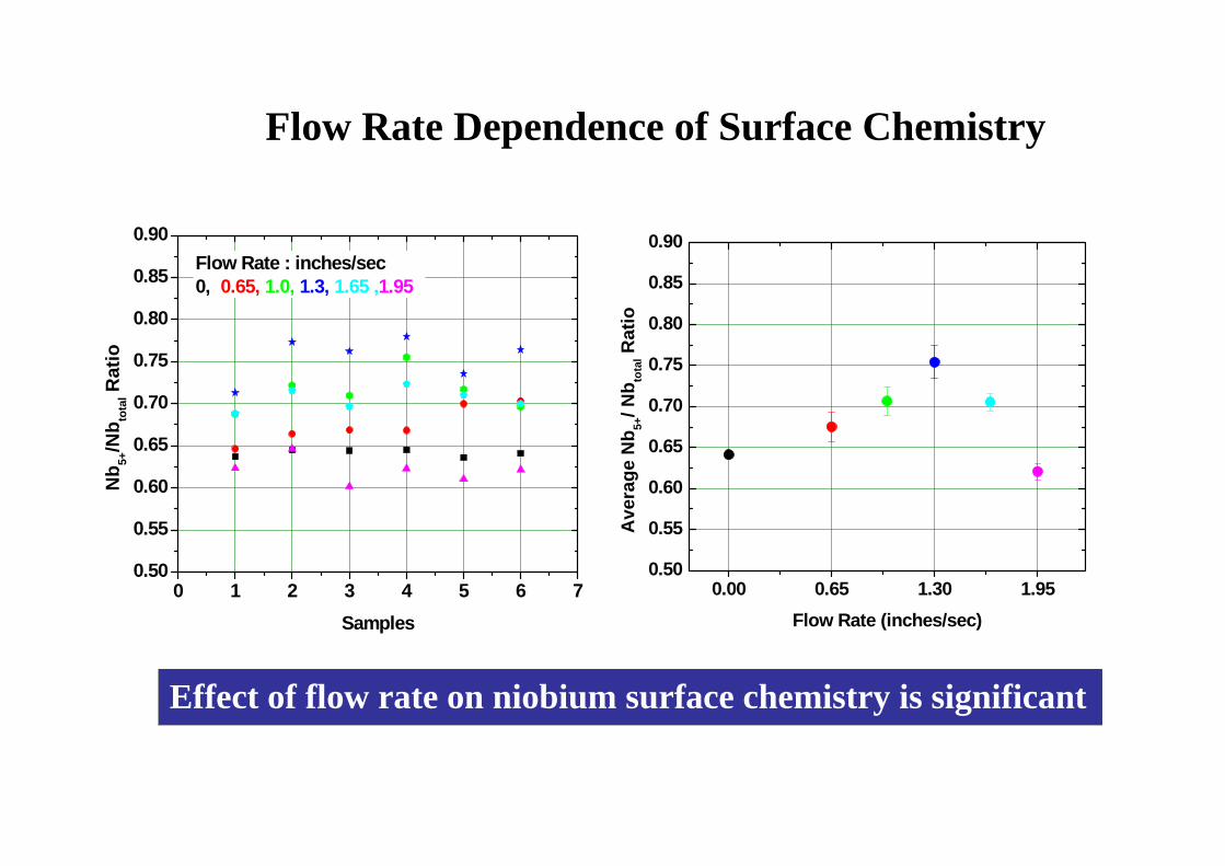
Flow Rate Dependence of Surface Topography
No significant effect of BCP flow rate on surface roughness .
Flow Rate Dependence of Surface ChemistryXPS measurement -relative Nb2O5 Thickness
1.0 inches/sec
Static
Nb5+hν = 930 eV
Takeoff angle = 0°
Nb2O5 is thicker on the high-flow sample
H. Tian, C. Reece , M. Kelley, et. al. Applied Surface Science, Vol. 253(3), 2006, p.1236-1242
Summary and Future Work
The effect of BCP on polycrystalline niobium surface have been systematically examined for the first time.
The micron-scale roughness does not change with treatment conditions. But the thickness of Nb2O5 increases with a range of realistic solution flow rate.
Future work:
A microscopic understanding of Nb BCP mechanism is important for optimizing the preparation of high gradient niobium cavity.
Outline: EP
1.Motivation-Understanding for Improving Performance.
2.Characterization of Niobium Surface Topography.
3.X-ray Photoelectron Spectroscopy (XPS) Studies of Niobium Surface Oxide.
4.Surface Study of Niobium Buffered Chemical Polished (BCP)Under Conditions for SRF Cavity Production.
5.Characterization of Niobium Electropolishing (EP).
0 2 4 6 8 10 12 14 16 18 200
5
10
15
20
25
30
35
40
Cur
rent
den
sity
( m
A/c
m2 )
Voltage ( power supply)
T = 31.5 +/- 0.5oC Reactive area = 5.72cm2
Electropolishing of Nb Cavity
Nb Sample I-Vpwrsup curve
12 ~25 V
30~5
0 m
A/ c
m2
Vpwsup= VNb-Veletrolyte-VAlCould not separate the impacts of anode (Nb), cathode (Al) and electrolyte individually . Impossible to clearly identify the local effect on Nb EP.
HF: H2SO4=1:9 (volume)
Al is cathode
Nb Cavity is anode
1 r/min
Power supply
9-Cell Nb Cavity Electropolishing @ Jefferson Lab
High purity Al tube inserted inside of cavity cell is cathode
Cavity is anode
The Large Performance Variation of EP Nb SRF Cavities
Microscopic understanding of the basic Nb EP mechanism is expected to provide an appropriate foundation with which to optimize the preparation of high-field niobium cavity surfaces. .
BCP
EP
Nb cavity performance after BCP/EP. Courtesy of www.linearcollider.org
-4 -2 0 2 4 6 8 10 12 14 16 18 200
5
10
15
20
25
30
35
40
Cur
rent
den
sity
( m
A/c
m2 )
Voltage ( vs. MSE )
T = 31.5 +/- 0.5oC Reactive area = 5.72cm2
“Three-Electrode-Setup” Improved Electrochemical Characterization of EP
Enables study of temperature, flow, and composition dependent effects(electrolyte) in detail.
“Three-electrode-setup ”separates impacts of individual components in EP system.
Example:VPwrSup = 15 V ; Vcathode : ~ 4 V Velectrolyte: ~ 2 V; Vanode:~ 9V
0 2 4 6 8 10 12 14 16 180
20
40
60
80
100
21.3 oC26.3 oC
33.5 oC
45.6 oC
54.6 oC
1 54.6 o C; 3 33.5 o C 2 45.6 o C; 4 26.3 o C 5 21.3 o C
Ano
de C
urre
nt D
ensi
ty (
mA
/cm
2 )
VNb( V ) (vs. MSE )20 30 40 50 60
0
20
40
60
80
100
Ano
de C
urre
nt D
ensi
ty (m
A/c
m2 )
Temperature ( oC )
SNb/ SAl = 10 : 1
Anode Current Density Strongly Depends on Local Temperature
Past studies identified 25-35 ºC for best EP gloss on Nb surface
For cavity EP, electrolyte also serves as the process coolant. Unstable temperatures is expected and particularly hot in no-flow condition and higher heat flux where flow rate is high. Non-uniform polishing is expected.
0.2 0.4 0.6 0.8 1.00
5
10
15
20
25
23.44 mA/cm2
Concentration of HF ( by volume )
5.27 mA/cm2
Anode Current Density Varies Linearly with HF Acid Volume Concentration
0 2 4 6 8 10 12 14 16 180
5
10
15
20
25
30
35
40
0.2:9.8
0.4:9.6
0.6:9.4
0.8:9.2
Ano
de C
urre
nt D
ensi
ty (
mA
/cm
2 )
Voltage ( V ) (vs. MSE)
Area ratio of Nb/Al =10:1T = 31.5+/- 1.5 oC
1:9
HF acid loss may be expected due to evaporation and chemical reaction during process. The understanding of the detailed role of HF involved during the EP process requires further electrochemical studies.
* Fresh mixture exposured under chemical hood for 5 hrs)
Ano
de P
late
au C
urre
nt D
ensi
ty (
mA
/cm
2 )10
V v
s. M
SE
Different volume ratio of H2O
2
Additional Volume H2O slightly Increases Anode Current Density
Anode current density slightly increases with additional volume of H2O (38~42%); Compare curve 1 and curve 2( after 5 hrs exposure under chemical hood), current density decreases 30 % -HF evaporation
Current-Limited Plateau of Nb EPMass Transport Mechanism Has Been Unknown
Micro-polishing (brightening) only occurs when the plateau is the result of diffusion-limitation alone. Understanding of mass transport mechanism requires further electrochemical study-EIS.
Possible mass transport limiting species proposed -D. Landolt, Electrochemica Acta, Vol . 32(1)
I) Metal Ions (Mn+aq) II) Acceptor anion (A-) III) H2O
CstCst
Cst
Maq
Maq
MAy
Con
cent
ratio
n
diffusion layerdiffusion layer diffusion layer
What is Electrochemical Impedance Spectroscopy?
Investigate the electrical dynamics of niobium-acid interaction during electropolishing.
EIS: 10 mV variable-frequency ac superimposed on normal dc polarization voltage; record the impedance at the different frequency.
Nyquist PlotRp: Polarization Resistor
Cdl :Capacitor of Electrode Surface
Rwarburg: Diffusion Resistor
Rs: Solution Resistor
Nb Ref. Elec.
EIS
Possible equivalent circuit of Nb-acid interface during EP
High Frequency Nyquist Plot
222
2
222 11 pdl
pdls
pdl
p
RCRC
jRRC
RZ
ωω
ω +−+
+=
ReZ
-ImZ
Zreal (Ω)Rs remains constant
-Zim
ag(
Ω)EIS Study of Constant Current Density
0 2 4 6 8 10 12 14 16 180
5
10
15
20
25Area Ratio of Nb/Al = 10 : 1 (Nb : 26.035 cm 2; Al : 2.6035 cm 2)Ref electrode & Thermal Couple nearby Nb ( < 5 mm ) T = 21.5 o C
Ano
de C
urre
nt D
ensi
ty (
mA
/cm
2 )
Anode Potential ( V )
Rp increases with the potential
0.2 Hz
200 KHz
1.01 KHz =ωmax=1/RpCdl
0.2 Hz
EIS Study of Different Flow Rates
Zreal (Ω)
-Zim
ag(
Ω)
Static (triangle) vs. Agitation (dot)(dot)
flow rate ~ 4 ~ 5 cm/sec
T = 9.2± 0.1 ºC
Rs @ at different flow condition remains as constant
3V 6V
Static
Flow
Rp decreases with increasing flow
200 KHz
0.2 Hz
0.2 Hz0.2 Hz
0.2 Hz
3 4 5 6 7
1.0
1.5
2.0
2.5
3.0
3.5
4.0
4.5
5.0
Cap
acita
nce
(µF
)
Potential ( V )
T = 9.0 +/- 0.2 oC Without agitationwith agitation ( flow rate : v ~ 4 ~ 5 cm/sec)
What We have Learned from EIS Studies?
Constant Rs at different potential regions and flow condition rules out the “porous salt film” model.
Rp ↑ at different potential regions is inconsistent with the “adsorbates acceptor” model.
3 4 5 6 76
8
10
12
14
16
18
20
22
24 T = 9.0 +/- 0.2 oC Without agitationwith agitation ( flow rate : v ~ 4 ~ 5 cm/sec)
Pola
rizat
ion
resi
stan
ce (o
hms)
Potential ( V )
Cdl ↓ at different potential regions & Cdl↑at different flow conditions are consistent with the “compact salt film” model.
EIS Indicates “Compact Salt Film” Model
Sulfuric acid tends to anodize the Nbunder polarization potential producing the "compact salt film”- “Nb2O5”.
HF acid tends to dissolve the Nb oxide under kinetic control with the "at the surface" concentration of F-
.
F- concentration “at the surface” is limited by how fast it diffuses through the electrolyte ( ~diffusion layer).
The local gradient in F- concentration produces the desired polishing action.
H. Tian, S. Cocoran, C. Reece, M. Kelley, Journal of the Electrochemical Society ( submitted)
diffusion layercompact film
“Nb2O5”
The Diffusion-Limited Access of F- To the Salt Film Produces Best Polishing
NbBulk Electrolyte
Diffusion Layer(~ um)
Compact Salt Film(~ nm)
F -
%
F -
%Distance
Distance
Local temperature, flow & electrolyte composition affect the local F- gradient
Summary and Future Work
The first use of “three-electrode-setup” reveals that Nb EP strongly depends on the local electrolyte temperature and HF/H2SO4 volume ratio.
High frequency impedance data provide strong evidence for the presence of a compact salt film (Nb2O5) in the current-limited plateau region.
The results suggest that the diffusion-limited access of the F- anion to the salt film surface limits the local reaction rate, creates the plateau and yields the micropolishing.
Future work:
Monitor polishing effect with different concentration HF acid, different flow rate, different temperature electrolyte and different process voltage specify optimum processing protocol.
Simulation & develop feedback to monitor cavity process.
Acknowledgements Advisor: Dr. Michael Kelley
Dr. Charles Reece
Committees: Dr. Sean Corcoran; Dr. Gunter Lüepke
J-Lab: Dr. Larry Philips, Dr. Peter KneiselDr. Gigi Ciovati; Dr. John MammosserDr. Rongli Geng; Dr. Xin ZhaoAnne-Marie Valente-Feliciano; Will SommerDr. Joan Thomas; Dr. Andy Wu
X1B(Boston Univ.): Dr. Kevin Smith; Dr. Cormac McGuinness; Dr. Per Anders Glans; Dr. Lukasz PlucinskiDr. Shangcai Wang; Dr. Yufeng Zhang Dr. Louis Piper; Alexander DeMasi
W&M: Dr. Ron Outlaw; Dr. Zhengmao Zhu; Dr. Haijian Chen; Dr. Mingyao Zhu Binping Xiao; Amy Wilkerson; Olga Trofimova
NCSU: Dr. Fred Stevie; Dr. Phil Russell; Dr. Dieter Griffis; Dr. Dale BatchelorGuilhem Ribeill
My families and friends for your constant support and pray!
“Oxygen Diffusion” Under Different Baking Duration
interstitial oxygen ( 10%) ?Nb2O5 reduction ?
Before Baking
After Baking
XPS Sampling depth (hυ= 750 eV )
2
2 ),()(),(x
txcTDt
txc∂
∂=
∂∂
),(),(),( txvtxutxc +=
Courtesy of G. Ciovati , internal talk , Jefferson lab
Oxides Structure (Unbaked/Baked)preliminary TEM results
baked
No clear structure change can be observed (suboxide, interstitial oxygen- cluster)
unbaked
Potentiostat PrimerA simplified schematic of Potentiostat
A working electrode - where the potential is controlled & the current is measured, serves as a surface on which the electrochemical reaction takes place.
The reference electrode : used in measuring the working electrode potential and have a constant electrochemical potential as long as no current flows through it.
An Auxiliary electrode ( counter electrode) : a conductor that completes the cell circuit.
Control amplifier- the cell voltage is controlled to be identical to the signal source voltage.
non-invert
invert The electrometer circuit measures the voltage difference between RE & WE It has zero input current and an infinite input impedance.
The Current-to-Voltage (I/E) converter in the simplified schematic measures the cell current.
The Electrode-Electrolyte Double Layer
The electron-electrolyte interface behave like a capacitor .
Nb
HF+H2SO4+H2O
Ionization: 1) metal ion move through electrolyte with applied potential. 2) electron recombine with positive ion 3) water dipoles and negative ions drag metal ions into electrolyte.
IHP/ OHP : inner/outer Helmholtz plate
IHL: water dipoles and some negative ions
OHL: solvated ion, the interaction with charged metal surface by long range electrostatic force
Diffuse layer
Effect of Electrolyte Temperature
The strong dependence of the measured anode current density on the local electrolyte temperature is observed; power dissipated at the cathode increases with electrolyte temperatures.
0 2 4 6 8 10 12 14 16 180
20
40
60
80
100
21.3 oC26.3 oC
33.5 oC
45.6 oC
54.6 oC
1 54.6 o C; 3 33.5 o C 2 45.6 o C; 4 26.3 o C 5 21.3 o C
Ano
de C
urre
nt D
ensi
ty (
mA
/cm
2 )
VNb( V ) (vs. MSE )-8 -7 -6 -5 -4 -3 -2 -1
0.0
0.5
1.0
1.5
2.0
2.5
21.3 oC
26.3 oC33.5 oC
45.6 oC
54.6 oC
1 54.6 o C; 3 33.5 o C 2 45.6 o C; 4 26.3 o C 5 21.3 o C
cath
ode
curr
ent (
A )
VAl( V ) vs. MSE
0 2 4 6 8 10 12 14 16 18 200
4
8
12
16
20
24
28
32
Area ratio of Nb/ AlT = 20.5 +/- 1.3 o C Cathode area (Al) kept unchanged ( 2.6cm 2 )1 : 1 ; 2 : 1 ; 4 : 16 : 1 ; 8 : 1 ; 10 : 1
Ano
de c
urre
nt d
ensi
ty (m
A/c
m2 )
VNb (V) vs. MSE
a
0 2 4 6 8 10 12 14 16 18 200
4
8
12
16
20
24
28
Area ratio of Nb/ AlT = 19.7 +/- 1.7 o C Anode area(Nb) kept unchanged ( 2.6 cm 2 )1 : 1 ; 1: 2 ; 1 : 41: 6 ; 1 : 8 ; 1 : 10
A
node
cur
rent
Den
sity
( m
A/c
m2 )
VNb( V ) vs. MSE
b
Anode Current Density Does Not Depend on the Relative Area of Anode and Cathode
Anode current density remain constant
)()()()( xCxxCD
RTFz
xxCDxJ iii
iiii υφ
+∂
∂−
∂∂
−=
The Mass Transport Mechanisms
Migration, movement of ions driven by a gradient of electrical potential
Convection, natural convection driven by density gradient; forced convection( stirring, vibration)
Diffusion, movement of species ( ions, molecules ) driven by a gradient of chemical potential ( i.e. a concentration gradient )
Nernst-Planck equation (1-dimension)
iL= 0.62nFAD2/3ν-1/6ω1/2 (C0-C*)RDE
iL→ω1/2 →D
Possible Mass Transport Mechanisms
Duplex (compact + porous) salt film mechanism : Duplex (compact + porous) salt film mechanism : involves involves rate limiting diffusion of rate limiting diffusion of cationscations of the dissolving metalof the dissolving metal from anode into the bulk.from anode into the bulk.
Adsorbate acceptor mechanism : involves rate limiting diffusion acceptor anions (such as H2O) which are consumed at the anode by formation of complexes ( MA+z) or hydrated metal ions.hydrated metal ions.
Courtesy of M. Matlosz,Electrochimica Acta. Issue 4, Vol. 40, 1995, pp. 393
Pores of precipitates are Pores of precipitates are filled with electrolyte, anions filled with electrolyte, anions and and cationscations transport transport current by migration. ~ current by migration. ~ μμmm
The limited current The limited current --diffusion diffusion of acceptor species through of acceptor species through diffusion layer diffusion layer
The rate of transport of The rate of transport of cationscationsacross the diffusion layer into the across the diffusion layer into the bulk electrolyte limits the anodic bulk electrolyte limits the anodic dissolution ratedissolution rate