DEMOCRITUS UNIVERSITY OF THRACE DEPARTMENT OF ELECTRICAL AND COMPUTER ENGINEERING VLSI DESIGN SYSTEMS AND TESTING CENTER XANTHI, 67100, GREECE Survey of FPGA reconfigurable Systems: Hardware platforms and Software Edited by: Dimitrios Soudris, Democritus University of Thrace Supported by AMDREL: Architectures and Methodologies for Dynamic Reconfigurable Logic, IST-2001-34379
Transcript
DEMOCRITUS UNIVERSITY OF THRACE
DEPARTMENT OF ELECTRICAL AND COMPUTER ENGINEERING
VLSI DESIGN SYSTEMS AND TESTING CENTER
XANTHI, 67100, GREECE
Survey of FPGA reconfigurable Systems: Hardware platforms and
Software
Edited by: Dimitrios Soudris, Democritus University of Thrace
Supported by AMDREL: Architectures and Methodologies for Dynamic Reconfigurable Logic, IST-2001-34379
Survey of FPGA reconfigurable Systems: Hardware platforms and Software
2
1. Abstract This document contains both an introduction to FPGA technology that includes architecture, power consumption and configuration models, and a comprehensive survey of the existing fine-grain reconfigurable architectures that have emerged from both academia and industry. All aspects of the architectures, including logic block structure, interconnect, and configuration methods are presented in detail. Comparisons in terms of testability, technology portability, design flow completeness and configuration type are shown. Additionally, the implementation techniques and CAD tools (synthesizers, LUT-mapping tools and placement and routing tools) that have been developed to facilitate the implementation of a system in reconfigurable hardware by the industry (both by the FPGA manufacturers and third-party EDA tool vendors) and academia are described.
Survey of FPGA reconfigurable Systems: Hardware platforms and Software
3
2. List of Abbreviations AMDREL Architectures and Methodologies for Dynamic Reconfigurable Logic ALU Aritmetic Logic Unit ASIC Application Specific Integrated Circuit BEST Behavioural Extracting Synthesis Technology BLE Basic Logic Element BUFT 3-State Buffer CCCU Configuration Control and Caching Unit CLB Configurable Logic Block CLE Configurable Logic Element CMOS Complementary Metal Oxide Semiconductor CPLD Complex Programmable Logic Device CSE Configurable Sequential Element DCT Direct Cosine Transform DSP Digital Signal Processor EBR Embedded Block RAM ECU Execution Control Unit EDA Electronic Design Automation EPGA Embedded Programmable Gate Array ESB Embedded System Block F/F Flip-Flop FFT Fast Fourier Transform FIFO First Input First Output FIR Finite Impulse Response FPGA Field Programmable Gate Array GRM General Routing Matrix GUI Graphic User Interface HDL Hardware Description Language I/O Input/Output IBD Interface Based Design IDE Integrated Design Environment IIR Infinite Impulse Response IP Intellectual Property ISP In-System Programmable LAB Logic Array Block LC Logic Cell LCA Logic Cell Arrays LDG Logic Description Generator LE Logic Element LIFO Last Input First Output LUT Look-Up Table ML Memory Layer NMOS Negative Metal Oxide Semiconductor PFU Programmable Function Unit PLA Programmable Logic Array PPL Phase Locked Loop RA Reconfigurable Array RFU Reconfigurable Functional Unit RL Routing Layer RLB Routing and Logic Block ROM Read Only Memory
Survey of FPGA reconfigurable Systems: Hardware platforms and Software
4
RTL Register Transfer Level SoC System on Chip SoPC System on Programmable Chip SRAM Static Random Access Memory SRF Shadow Register File TOPS Total Optimization Physical Synthesis VLI Variable Length Interconnect
Survey of FPGA reconfigurable Systems: Hardware platforms and Software
5
3. List of Tables Table 1: Chip Characteristics ............................................................................................................................29 Table 2: Contribution of different components to the total area...................................................................34 Table 3: Execution Energy Per Data Token in pJ ..........................................................................................35 Table 4: Comparisons of fine-grain academic architectures ........................................................................38 Table 5: Products of the HyperBlox FP family................................................................................................79 Table 6: Function Capability of ispXPGA PFU ...............................................................................................80 Table 7: Comparison between some the most well-known FPGAs ............................................................84 Table 8: Lattice Software ...................................................................................................................................92 Table 9: Quartus II Verification Solutions ........................................................................................................97
Survey of FPGA reconfigurable Systems: Hardware platforms and Software
6
4. List of Figures Figure 1: FPGA Model .......................................................................................................................................11 Figure 2: Island style architecture ....................................................................................................................12 Figure 3: Row-based architecture ....................................................................................................................12 Figure 4: Sea-of-Gates Architecture ................................................................................................................13 Figure 5: Hierarchical architecture ...................................................................................................................13 Figure 6: One-dimensional structure................................................................................................................14 Figure 7: Mesh (left) and partial crossbar (right) interconnect topologies for multi-FPGA systems. ......15 Figure 8: Types of programmable switch used in SRAM-based FPGAs....................................................17 Figure 9: Power Breakdown in an XC4003 FPGA .........................................................................................18 Figure 10: Static Reconfiguration .....................................................................................................................19 Figure 11: Dynamic Reconfiguration................................................................................................................19 Figure 12: (a) The DECPeRLe-1 System Architecture, (b) The Central Matrix.........................................24 Figure 13: Basic Garp block diagram ..............................................................................................................25 Figure 14: Overview of the Chimaera Architecture........................................................................................26 Figure 15: DISC Architecture ............................................................................................................................27 Figure 16: Heterogeneous Reconfigurable Processor Architecture............................................................28 Figure 17: Heterogeneous Reconfigurable Processor Chip Microphotograph ..........................................29 Figure 18: Routing and Logic Block (RLB)......................................................................................................30 Figure 19: General architecture of UTFPGA1 ................................................................................................31 Figure 20: Logic Block Architecture .................................................................................................................32 Figure 21: Nearest neighbor connection .........................................................................................................33 Figure 22: Level-2 connections.........................................................................................................................33 Figure 23: The LP_PGAII layout of a single tile .............................................................................................34 Figure 24: Energy as a Function of Path Length............................................................................................35 Figure 25: Block diagram of the 3-D FPGA ....................................................................................................36 Figure 26: Internal Structure of the functional unit .........................................................................................37 Figure 27: Spartan/XL Simplified CLB Logic Diagram ..................................................................................39 Figure 28: Spartan-II CLB Slice ........................................................................................................................41 Figure 29: Virtex architecture overview ...........................................................................................................42 Figure 30: A 2-Slice Virtex CLB ........................................................................................................................43 Figure 31: Virtex-E Architecture Overview ......................................................................................................45 Figure 32: Virtex-II Architecture Overview ......................................................................................................46 Figure 33: Startix Logic Element ......................................................................................................................49 Figure 34: Apex_II Logic Element ....................................................................................................................51 Figure 35: Mercury Logic Element ...................................................................................................................54 Figure 36: FLEX 10K Logic Element................................................................................................................56 Figure 37: Flex 6000 Logic Element ................................................................................................................60 Figure 38: The Actel’s eX family logic modules - (a) R-Cell, and (b) C-Cell ..............................................62 Figure 39: Core Logic Tile for ProASIC 500K Family....................................................................................64 Figure 40: 40MX Logic Module .........................................................................................................................68 Figure 41: VariCore SRAM Architecture – A 4x4 array.................................................................................70 Figure 42: The EPGA Logic Unit ......................................................................................................................70 Figure 43: The AT6000 Series Cell Structure.................................................................................................73 Figure 44: (a) Eclipse SuperCell, (b) pASIC 1 Internal Logic Cell, and (c) pASIC 3 Family Logic Cell .74 Figure 45: The ispXPGA architecture ..............................................................................................................80 Figure 46: Traditional Design Synthesis Approach and the Modeling Approach ......................................85 Figure 47: The CAD flow with the VPR tool ....................................................................................................89 Figure 48: Framework with power model ........................................................................................................89
Survey of FPGA reconfigurable Systems: Hardware platforms and Software
6.4. Power Dissipation .................................................................................................................17 6.4.1. Components of Power .................................................................................................18 6.4.2. Interconnect Energy.....................................................................................................18 6.4.3. Clock Energy................................................................................................................18
9.2. Public Domain Tools.............................................................................................................86 9.2.1. Tools from UCLA..........................................................................................................86 9.2.2. Tools from Toronto FPGA Research Group ................................................................87
Survey of FPGA reconfigurable Systems: Hardware platforms and Software
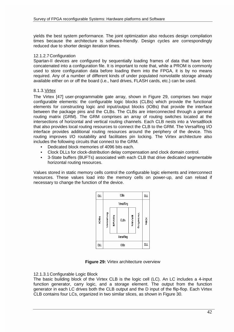
9
10. Commercial Software tools for designing fine-grain platforms ...........................................90
10.1. Actel..................................................................................................................................90 10.1.1. Development Software.................................................................................................90 10.1.2. Programming................................................................................................................90 10.1.3. Verification and Debug.................................................................................................91 10.1.4. Device Support.............................................................................................................91
Survey of FPGA reconfigurable Systems: Hardware platforms and Software
10
6. Introduction to FPGAs The Field Programmable Gate Array (FPGA) is an important technology, which allows circuit designers to produce application-specific chips around the time-consuming fabrication process. When FPGAs were first introduced in the mid 1980s they were viewed as a technology for replacing standard gate arrays for some applications. In these first-generation systems, a single configuration is created for the FPGA, and this configuration is the only one loaded into the FPGA. A second generation soon followed, with FPGAs that could use multiple configurations, but reconfiguration was done relatively infrequently. In such systems, the time to reconfigure the FPGA was of little concern. Nowadays, the applications demand short time for reconfiguration and so a new generation of FPGAs was developed that could support many types of reconfiguration methods, depending to the application specific needs. Those types of reconfiguration are described also briefly this survey. The first part of this report describes the Field Programmable Gate Arrays (FPGA) at the field of the existing interconnect architectures, the architecture of the logic block, the existing programming technologies, the power dissipation and the reconfigurable models. Next follows a description of the available commercial and academic fine-grain reconfigurable architectures. The third part of this document presents the available CAD tools, used for programming FPGAs. Those tools are separated in commercial ones and those that are public domain and referred as academic. Finally, there is a conclusion where remarkable results are exhibited. An FPGA can be programmed to solve a problem at hand in a spatial fashion. The goal of reconfigurable architectures is to achieve implementation efficiency approaching that of specialized logic, while providing the silicon reusability of general-purpose processors. The main characteristics of an FPGA that will be described below are:
• The interconnect architecture • The logic block architecture • The programming technology • The power dissipation • The existing reconfigurable models
FPGA can be visualized as a programmable logic embedded in programmable interconnect. All FPGAs are composed of three fundamental components: logic blocks, I/O blocks and programmable routing. A circuit is implemented in an FPGA by programming each logic block to implement a small portion of the logic required by the circuit, and each of the I/O blocks to act as either an input pad or an output pad, as required by the circuit. The programmable routing is configured to make all the necessary connections between logic blocks and from logic blocks to I/O blocks. The functional complexity of logic blocks can vary from simple two-input Boolean operations to larger, complex, multi-bit arithmetic operations. The choice of the logic block granularity is dependent on the target application domain. The programming technology determines the method of storing the configuration information, and comes in different flavors. It has a strong impact on the area and performance of the array. The main programming technologies are: Static Random Access Memory (SRAM) [1], antifuse [2], and non-volatile technologies. The choice of the programming technology is based on the computation environment in which the FPGA is used.
Survey of FPGA reconfigurable Systems: Hardware platforms and Software
11
Figure 1: FPGA Model
The general model of an FPGA is shown in Figure 1. The logic cell usually consists of lookup tables (LUTs), carry logic, flip-flops, and programmable multiplexers. The multiplexers are utilized to form data-paths inside the logic cell and to connect the logic cells with the interconnection resources.
6.1. Interconnect Architecture (Routing Resources) The interconnect architecture is realized using switches that can be programmed to realize different connections. The method of providing the connectivity between the logic blocks has a strong impact on the characteristics of the FPGA architecture. The arrangement of the logic and interconnect resources can be broadly classified into six groups:
• Island style • Row-based • Sea-of-gates • Hierarchical • One-dimensional structures • Multi-FPGA systems
Commercial FPGAs can be classified into three groups, based on their routing architecture. The FPGAs of Xilinx, Lucent and Vantis are island-style FPGAs, while Actel’s FPGAs are row-based, and Altera’s FPGAs are hierarchical.
6.1.1. Island Style Architecture The island style architecture consists of an array of programmable logic blocks with vertical and horizontal programmable routing channels. The basic architecture is illustrated in Figure 2. The number of segments in the channel determines the resources available for routing. This is quantified in terms of the channel width. The pins of the logic block can access the routing channel through the connection box. The XC4000 and XC3000 series from Xilinx [3] are examples of this kind of architecture.
Survey of FPGA reconfigurable Systems: Hardware platforms and Software
12
Figure 2: Island style architecture
6.1.2. Row-Based Architecture As the name implies, this architecture has logic blocks arranged in rows with horizontal routing channel between successive rows. The row-based architecture is shown in Figure 3. The routing tracks within the channel are divided into one or more segments. The length of the segments can vary from the width of a module pair to the full length of the channel. The segments can be connected at the ends using programmable switches to increase their length. Other tracks run vertically through the logic blocks. They provide connections between the horizontal routing channel and the vertical routing segments. The length of the wiring segments in the channel is determined by tradeoffs involving the number of tracks, the resistance of the routing switches, and the capacitance of the segments. The ACT3 family of FPGAs from Actel [4] is an example of this architecture.
Figure 3: Row-based architecture
Survey of FPGA reconfigurable Systems: Hardware platforms and Software
13
6.1.3. Sea-of-Gates Architecture The sea-of-gates architecture, as shown in Figure 4, unlike the previous architectures, is not an array of logic blocks embedded in a general routing structure. The architecture consists of fine-grain logic blocks covering the entire floor of the device. Connectivity is realized using dedicated neighbor-to-neighbor routes that are usually faster than general routing resources. Usually the architecture also uses some general routes to realize longer connections. The SX family of FPGAs from Actel [5] is an example of this class of architecture.
Figure 4: Sea-of-Gates Architecture
6.1.4. Hierarchical Architecture Most logic designs exhibit locality of connections, which imply a hierarchy in the placement and routing of the connections between the logic blocks. The hierarchical FPGA architecture tries to exploit this feature to provide smaller routing delays and a more predictable timing behavior. This architecture is created by connecting logic blocks into clusters. These clusters are recursively connected to form a hierarchical structure. Figure 5 illustrates a possible architecture. The speed of the network is determined by the number of routing switches it has to pass through. The hierarchical structure reduces the number of switches in series for long connections and can hence potentially run at a higher speed.
Figure 5: Hierarchical architecture
Survey of FPGA reconfigurable Systems: Hardware platforms and Software
14
6.1.5. One-Dimensional Structures Most current FPGAs are of the two-dimensional variety. This allows for a great deal of flexibility, as any signal can be routed on a nearly arbitrary path. However, providing this level of routing, flexibility requires a great deal of routing area. Also complicates the placement and routing software, as the software must consider a very large number of possibilities. One solution is to use a more one-dimensional style of architecture, as shown in Figure 6. Here placement is restricted along one axis. With a more limited set of choices, the placement can be performed much more quickly. Routing is also simplified, because it is generally along a single dimension as well, with the other dimension generally only used for calculations requiring a shift operation. One drawback of the one-dimensional routing is that if there are not enough routing resources for a specific area of a mapped circuit, then the routing of the whole circuit becomes actually more difficult than on a two-dimensional array that provides more alternatives. A number of reconfigurable systems have been designed by this manner, like Garp [31], Chimaera [20] [33] and NAPA [22].
Figure 6: One-dimensional structure
6.1.6. Multi-FPGA Systems Reconfigurable systems that are composed of multiple FPGA chips interconnected on a single processing board have additional hardware concerns over a single-chip system. In particular, there is a need for an efficient connection scheme between the chips, as well as to external memory and the system bus. This is to provide for circuits that are too large to fit within a single FPGA, but may be partitioned over the multiple FPGAs available. A number of different interconnect schemes have been explored [6] [7] [8] [9] including meshes and crossbars, as shown in Figure 7. A mesh connects the nearest-neighbors in the array of FPGA chips. This allows for efficient communication between the neighbors, but may require that some signals pass through an FPGA simply to create a connection between non-neighbors. Although this can be done, and is quite possible, it uses valuable I/O resources on the FPGA that forms the routing bridge. A crossbar attempts to remove this problem by using special routing-only chips to connect each FPGA potentially to any other FPGA. The inter-chip delays are more uniform, given that a signal travels the exact same “distance” to get from one FPGA to another, regardless of where those FPGAs are located. However, a crossbar interconnect does not scale easily with an increase in the number of FPGAs. The crossbar pattern of the chips is fixed at fabrication of the multi-FPGA board. For multi-FPGA systems, because of the need for efficient communication between the FPGAs, determining the inter-chip routing topology is a very important step in the design process.
Survey of FPGA reconfigurable Systems: Hardware platforms and Software
15
Figure 7: Mesh (left) and partial crossbar (right) interconnect topologies for multi-FPGA systems.
6.2. Logic Block Architecture The logic block, which is also known as configurable logic block (CLB), is responsible for implementing the gate level functionality required for each application. The logic block is defined by its internal structure and the granularity. The structure defines the different kinds of logic that can be implemented in the block, while the granularity defines the size of the function that can be implemented. The functionality of the logic block is obtained by controlling the connectivity of some basic logic gates or by using LUTs and has a direct impact on the routing resources. As the functional capability increases, the amount of logic that can be packed into it increases. This reduces the amount of external routing resources. On the other hand, as the logic block size increases, it is also quite possible that the block can not be fully utilized, resulting in wastage. Based on this tradeoff, there are numerous logic block structures trying to optimize the area and speed of the FPGA [41]. A collection of CLBs, which could be called as logic cluster, is described with the following four parameters:
• The size of (number of inputs to) a LUT. • The number of CLBs in a cluster. • The number of inputs to the cluster for use as inputs by the LUTs. • The number of clock inputs to a cluster (for use by the registers).
The advantage of using a k-input LUT (k-LUT) is that it can realize any combinational logic with k inputs. Previous work [10] that evaluated the effect of the logic block on the FPGA architecture used a k-input LUT with a single output as the logic block. This structure is better for implementing random logic functions than for datapath-like bit-slice operations.
6.2.1. Logic Block Granularity The logic blocks vary in complexity from a very small and simple block that can calculate a function of only three inputs, to a structure that is essentially a 4-bit ALU. The size and complexity of the basic computing blocks is referred to as the block’s granularity. In other words, the granularity criterion reflects to the smallest block of which a reconfigurable device is made. The choice in the logic block granularity is influenced by the application space envisioned for the FPGA, and it has a potential effect on the reconfiguration time of the device. This is an important issue especially for run-time reconfiguration systems. All the reconfigurable platforms based on their granularity are distinguished into two groups, the fine-grain and coarse-grain systems. In fine-grained architectures, the basic programmed building block consists of a combinatorial network and a few flip-flops. A fine-grain array has many configuration points to perform very small computations, and thus requires more data bits during configuration. The fine-grain programmability is more amenable to control
Survey of FPGA reconfigurable Systems: Hardware platforms and Software
16
functions, while the coarser grain blocks with arithmetic capability are more useful for datapath operations. All the reconfigurable architectures that are described in this report are characterized as fine-grain reconfigurable architectures. This term is traditionally used when the hardware architecture implements bit-level functions. Nowadays, where the need for high speed calculations is critical, many of the existing reconfigurable hardware use more than one bit for the functions that they implement. Even though this hardware can be characterized as coarse-grain, we believe, we propose to describe hardware platforms that are based on one or two-bit functions as fine-grain architectures, while all the others are supposed to be coarse-grain ones.
6.2.2. Studies on the CLB Structure Studies on the CLB structure have shown that the best number of inputs to use in order to improve area is between 3 and 4 [10]. Also it is possible to improve the functionality by including a D flip-flop. Moreover, for multiple output LUTs, the use of 4-input LUT could minimize the area [10], while the 5 and 6 inputs LUT minimize the delay [13]. The use of heterogeneous logic blocks that have combination of 4 and 6 inputs LUTs shown that it has the same area as the 4-inputs LUTs, but it has improved the speed by 25% [14]. Finally, the use of clusters with 4-inputs LUT instead of one 4-input LUT, results in a decrease of 10% at area [15].
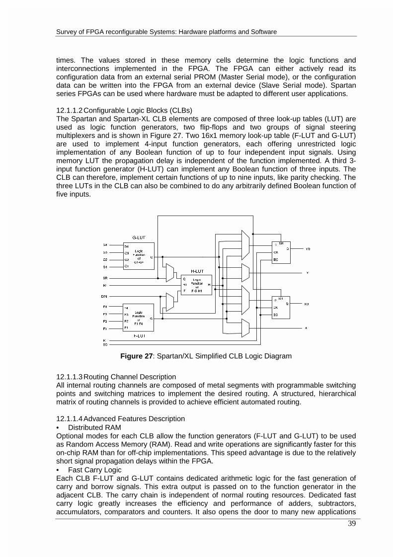
6.3. Programming Technology The logic and routing resources of an FPGA are uncommitted, and must be programmed to realize the required behavior. The contents of the logic block can be programmed to control the functionality of the logic block, while the routing switches can be programmed to control the connections between the logic blocks. There are a number of different methods to store this program information, ranging from the volatile SRAM method to the irreversible antifuse technology. The area of an FPGA is dominated by the area of the programmable components. Hence, the choice of the programming technology can also affect the area of the FPGA. Another factor that has to be considered is the number of times the FPGA has to be programmed. The antifuse-based FPGA can be programmed only once, while the SRAM-based FPGA does not limit the number of times the array can be reprogrammed.
6.3.1. SRAM In this method of programming, the configuration is stored in SRAM cells. When the interconnect network is implemented using pass-transistors, the SRAM cells control whether the transistor is on or off. In the case of the lookup tables used in the logic block, the logic is stored in the SRAM cells. This method suffers from the fact that the storage is volatile and the configuration has to be written into the FPGA each time on power-up. For systems using SRAM-based FPGAs, an external permanent storage device is usually used. This technology requires at least five transistors per cell. Due to the relatively large size of the memory cells, the area of the FPGA is dominated by configuration storage. The SRAM method of programming offers the convenience of reusing a single device for implementing different applications by loading different configurations. This characteristic has made SRAM-based FPGAs popular in reconfigurable platforms, which strive to obtain performance gains by customizing the implementation of functions to the specific application. Figure 8 shows these SRAM-based switches, where the pass gates are implemented with nMOS pass transistors, rather than complementary transmission gates, as this results in better speed due to the higher carrier mobility in nMOS transistors.
Survey of FPGA reconfigurable Systems: Hardware platforms and Software
17
Figure 8: Types of programmable switch used in SRAM-based FPGAs
6.3.2. Antifuse In the SRAM programming method, the information is stored by controlling the state of the memory cell. The antifuse programming method [84] uses a programmable connection whose impedance changes on the application of a high voltage. In the un-programmed state, the impedance of the connection is of the order of a few giga-ohms, and can be treated as an open circuit. By applying a high voltage, a physical change called fusing occurs. This result in an impedance of a few ohms though the device, establishing a connection. This method has the advantage that the area of the programming element is of the order of the size of a Via, and therefore can achieve a significant reduction in area compared to the SRAM-programmed FPGA. The resistance through the element is of the order of a few ohms and is much smaller than the resistance of a pass-transistor that is used as the routing switch in the SRAM method. This programming technique is non-volatile, and does not require external configuration storage on power-down. Unlike the SRAM based technology, errors in the design cannot be corrected, since the programming process is irreversible.
6.3.3. EPROM, EEPROM, and FLASH This class of non-volatile programming technology uses the same techniques as EPROM, EEPROM and Flash memory technologies. This method is based on a special transistor with two gates: a floating gate and a select gate. When a large current flows through the transistor, a charge is trapped in the floating gate that increases the threshold voltage of the transistor. Under normal operation, the programmed transistors may act as open circuits, while the other transistors can be controlled using the select gates. The charge under the floating gate will persist during power-down. The floating charge can be removed by exposing the gate to the ultraviolet light in the case of EPROMs, and by electrical means in the case of EEPROMs and Flash. These techniques straddle the middle ground between the SRAM and antifuse techniques. They provide the non-volatility of antifuse with the reprogrammability of SRAM. The resistance of the routing switches is larger than that of the antifuse, while the programming is more complex and time consuming than that of the SRAM technique.
6.4. Power Dissipation Today’s reconfigurable systems have become more complex, and can take advantage of the programmability offered by the Field-Programmable Gate Arrays. This environment places stress on the energy efficiency of FPGAs, which has not been solved in existing commercial architectures. Another factor that has gained importance is the power density of the integrated circuits. With the reduction in feature size the transistor count per die have increased. This has resulted in an increase of power density, and the overall power dissipation per chip. Recently, some academic research attempts concern the issue of power dissipation reduction [41]. This trend will continue, and has implications on the economics and technology of packaging these devices.
Survey of FPGA reconfigurable Systems: Hardware platforms and Software
18
6.4.1. Components of Power A dramatic improvement in energy efficiency of FPGAs is required. An understanding of the energy breakdown in an FPGA is required to enable an efficient redesign process. Figure 9 gives the energy breakdown of an XC4003 FPGA over a set of benchmark netlists [16].
In te rco n n e ct65%
Clo ck21%
IO9%
Lo g ic5%
Figure 9: Power Breakdown in an XC4003 FPGA
The majority of the power is dissipated in the interconnection. The next major component is the clock network, while the logic block consumes only 5% of the total energy. This breakdown is not specific to the Xilinx FPGA, but is representative of most of the commercial FPGA architectures.
6.4.2. Interconnect Energy The term “interconnect” include all the resources required to realize a connection between two logic blocks. The physical realization of the connection involves metal tracks and programmable switches that have to be activated. The capacitance on the line comes from the metal track spanning one logic block, and from the diffusion capacitances of the pass transistors connected to this metal track. This can be reduced by either decreasing the number of switches accessing the line, or by making the transistors smaller. The number of switches can be decreased by reducing the flexibility of the switch box and the connection box, and by reducing the width of the routing channel. Any modification of the flexibility has to be accompanied by an evaluation of the routing efficiency of the entire architecture. The interconnect path in an FPGA can be modeled as an RC chain. The resistance of the series transistors contributes to the R, while the diffusion capacitance of the nMOS transistors in the path contributes to the C. By reducing the width of the switch, the R of the series path increases, reducing the speed performance.
6.4.3. Clock Energy The next major contributor to the total energy is the clock. Typically in all FPGAs, flip-flops are provided in each logic block to register the output. The availability of flip-flops in each logic block improves the utilization of the array, and leads to a better area efficiency. A side effect to this architectural decision is that the clock has to be distributed over the entire array to supply the sparse distribution of flip-flops. This results in a relatively large cost for the clock distribution network. For the clock energy, the dominant component is actually the distribution network, and not the load presented by the flip-flops. Hence, the distribution network has to be targeted first to reduce the clock energy.
Survey of FPGA reconfigurable Systems: Hardware platforms and Software
19
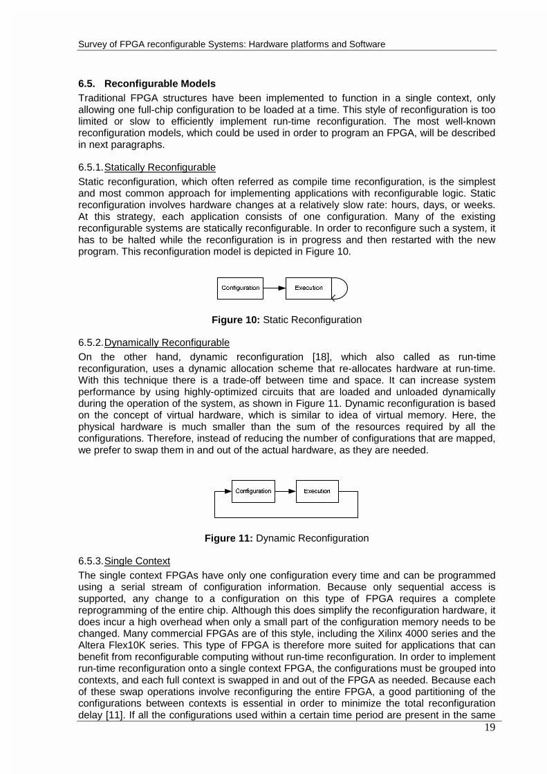
6.5. Reconfigurable Models Traditional FPGA structures have been implemented to function in a single context, only allowing one full-chip configuration to be loaded at a time. This style of reconfiguration is too limited or slow to efficiently implement run-time reconfiguration. The most well-known reconfiguration models, which could be used in order to program an FPGA, will be described in next paragraphs.
6.5.1. Statically Reconfigurable Static reconfiguration, which often referred as compile time reconfiguration, is the simplest and most common approach for implementing applications with reconfigurable logic. Static reconfiguration involves hardware changes at a relatively slow rate: hours, days, or weeks. At this strategy, each application consists of one configuration. Many of the existing reconfigurable systems are statically reconfigurable. In order to reconfigure such a system, it has to be halted while the reconfiguration is in progress and then restarted with the new program. This reconfiguration model is depicted in Figure 10.
Figure 10: Static Reconfiguration
6.5.2. Dynamically Reconfigurable On the other hand, dynamic reconfiguration [18], which also called as run-time reconfiguration, uses a dynamic allocation scheme that re-allocates hardware at run-time. With this technique there is a trade-off between time and space. It can increase system performance by using highly-optimized circuits that are loaded and unloaded dynamically during the operation of the system, as shown in Figure 11. Dynamic reconfiguration is based on the concept of virtual hardware, which is similar to idea of virtual memory. Here, the physical hardware is much smaller than the sum of the resources required by all the configurations. Therefore, instead of reducing the number of configurations that are mapped, we prefer to swap them in and out of the actual hardware, as they are needed.
Figure 11: Dynamic Reconfiguration
6.5.3. Single Context The single context FPGAs have only one configuration every time and can be programmed using a serial stream of configuration information. Because only sequential access is supported, any change to a configuration on this type of FPGA requires a complete reprogramming of the entire chip. Although this does simplify the reconfiguration hardware, it does incur a high overhead when only a small part of the configuration memory needs to be changed. Many commercial FPGAs are of this style, including the Xilinx 4000 series and the Altera Flex10K series. This type of FPGA is therefore more suited for applications that can benefit from reconfigurable computing without run-time reconfiguration. In order to implement run-time reconfiguration onto a single context FPGA, the configurations must be grouped into contexts, and each full context is swapped in and out of the FPGA as needed. Because each of these swap operations involve reconfiguring the entire FPGA, a good partitioning of the configurations between contexts is essential in order to minimize the total reconfiguration delay [11]. If all the configurations used within a certain time period are present in the same
Survey of FPGA reconfigurable Systems: Hardware platforms and Software
20
context, no reconfiguration will be necessary. However, if a number of successive configurations are each partitioned into different contexts, several reconfigurations will be needed, slowing the operation of the run-time reconfigurable system.
6.5.4. Multi-Context A multi-context FPGA includes multiple memory bits for each programming bit location [19]. These memory bits can be thought of as multiple planes of configuration information, each of which can be active at a given moment, but the device can quickly switch between different planes, or contexts, of already-programmed configurations. A multi-context device can be considered as a multiplexed set of single context devices, which requires that a context be fully reprogrammed to perform any modification. This system does allow for the background loading of a context, where one plane is active and in execution while an inactive place is the process of being programmed. Fast switching between contexts makes the grouping of the configurations into contexts slightly less critical, because if a configuration is on a different context than the one that is currently active, it can be activated within an order of nanoseconds, as opposed to milliseconds or longer. However, it is likely that the number of contexts within a given program is larger than the number of contexts available in the hardware. In this case, the partitioning again becomes important to ensure that configurations occurring in close temporal proximity are in a set of contexts that are loaded into the multi-contexts device at the same time.
6.5.5. Partially Reconfigurable In some cases, configurations do not occupy the full reconfigurable hardware, or only a part of a configuration requires modification. In both of these situations, a partial reconfiguration of the array is required, rather than the full reconfiguration required by a single-context or multi-context device. In a partially reconfigurable FPGA, the underlying programming bit layer operates like a RAM device. Using addresses to specify the target location of the configuration data allows for selective reconfiguration of the array. Frequently, the undisturbed portions of the array may continue execution, allowing the overlap of computation with reconfiguration. This has the benefit of potentially hiding some of the reconfiguration latency. When configurations do not require the entire area available within the array, a number of different configurations may be loaded into unused areas of the hardware at different times. Since only part of the array is reconfigured at a given point in time, the entire array does not require reprogramming. Additionally, some applications require the updating of only a portion of a mapped circuit, while the rest should remain intact. Using this selective reconfiguration can greatly reduce the amount of configuration data that must be transferred to the FPGA. Several run-time reconfigurable systems are based upon a partially reconfigurable design, including Chimaera [20] [33], PipeRench [21], NAPA [22], and the Xilinx 6200 and Virtex FPGAs [23] [24].Unfortunately, since address information must be supplied with configuration data, the total amount of information transferred to the reconfigurable hardware may be greater than what is required with a single context design. This makes the full reconfiguration of the entire array slower than the single context version. However, a partially reconfigurable design is intended for applications in which the size of the configurations is small enough that more than one can fit on the available hardware simultaneously.
6.5.6. Pipeline Reconfigurable A modification of the partially reconfigurable FPGA design is one in which the partial reconfiguration occurs in increments of pipeline [11] stages. Each stage is configured as a whole. This is primarily used in datapath style computations, where more pipeline stages are used than can be fitted simultaneously on available hardware. In a pipeline reconfigurable FPGA, there are two primary execution possibilities. Either the available number of hardware pipeline stages is greater than or equal to the number of pipeline stages of the designed
Survey of FPGA reconfigurable Systems: Hardware platforms and Software
21
circuit (virtual pipeline stages), or the number of virtual pipeline stages will exceed the number of hardware pipeline stages. The first case is straightforward: the circuit is simply mapped to the array, and some hardware stages may go unused. The second case is more complex and is the one that requires runtime reconfiguration. The pipeline stages are configured one by one, from the start of the pipeline, through the end of the available hardware stages. After each stage is programmed, it begins computation. In this manner, the configuration of a stage is exactly one step ahead of the flow of data. Once the hardware pipeline has been completely filled, reuse of the hardware pipeline stages begins.
6.6. Runtime Reconfiguration Categories The challenges associated with runtime reconfiguration are closely linked with the goal of reconfiguration. Therefore, it is important to consider the motivation and the different scenarios of runtime reconfiguration, which are algorithmic, architectural and functional reconfiguration. They are briefly described below.
6.6.1. Algorithmic Reconfiguration The goal in algorithmic reconfiguration is to reconfigure the system with a different computational algorithm that implements the same functionality, but with different performance, accuracy, power, or resource requirements. The need for such reconfiguration arises when either the dynamics of the environment or the operational requirements change.
6.6.2. Architectural Reconfiguration The goal in architectural reconfiguration is to modify the hardware topology and computation topology by reallocating resources to computations. The need for this type of reconfiguration arises in situations where some resources become unavailable either due to a fault or due to reallocation to a higher priority job, or due to a shutdown in order to minimize the power usage. For the system to keep functioning in spite of the fault the hardware topology need to be modified and the computational tasks need to be reassigned.
6.6.3. Functional Reconfiguration The goal in functional reconfiguration is to execute different function on the same resources. The need for this type of reconfiguration arises in situations where a large number of different functions are to be performed on a very limited resource envelope. In such situations the resources must be time-shared across different computational tasks to maximize resource utilization and minimize redundancy.
6.7. Fast Configuration Because run-time reconfigurable systems involve reconfiguration during program execution, the reconfiguration must be done as efficiently and as quickly as possible. This is in order to ensure that the overhead of the reconfiguration does not eclipse the benefit gained by hardware acceleration. Stalling execution of either the host processor or the reconfigurable hardware because of configuration is clearly undesirable. There are a number of different tactics for reducing the configuration overhead, and they will be described below.
6.7.1. Configuration Prefetching By loading a configuration into the reconfigurable logic in advance of when it is needed, it is possible to overlap the reconfiguration with useful computation. This results in a significant decrease in the reconfiguration overhead for these applications. Specifically, in systems with multiple contexts, partial run-time reconfigurability, or tightly coupled processors it is possible to load a configuration into all or part of the FPGA while other parts of the system continue computing. In this way, the reconfiguration latency is overlapped with useful computations, hiding the reconfiguration overhead. The challenge in configuration prefetching [25] is
Survey of FPGA reconfigurable Systems: Hardware platforms and Software
22
determining far enough in advance which configuration will be required next. Many computations (especially those found in general-purpose computations) can have very complex control flows, with multiple execution paths branching off from any point in the computation, each potentially leading to a different next configuration.
6.7.2. Configuration Compression When multiple contexts or configurations have to be loaded in quick succession then the system’s performance may not be satisfactory. In such a case, the delay incurred is minimized when the amount of data transferred from the processor to the reconfigurable hardware is minimized. A technique that could be used in order to compact this configuration information is the configuration compression [26]. In addition to that, a new configuration might reuse configuration information that is already present on the hardware, such that only the areas differing in configuration values must be reprogrammed. Moreover, by creating larger configurations out of groups of smaller configurations, the configuration overhead is reduced. This happens due to the fact that more operations can be present on chip simultaneously. On the other hand, a disadvantage of this method is that it has some area and execution penalties.
6.7.3. Relocation and Defragmentation in Partially Reconfigurable Systems Partially reconfigurable systems have advantages over single context systems, but problem might occur if two partial configurations are supposed to be located at overlapping physical locations on the FPGA. A solution to this problem is to allow the final placement of the configurations to occur at run-time, allowing for run-time relocation of those configurations. By using this technique, the new configuration could be placed onto the reconfigurable hardware where it will cause minimum conflict with other needed configurations already present on the hardware. A number of systems use the run-time relocation [27], among them are the Chimaera [20] [33], PipeRench [21] and Garp [31]. Over time, as a partially reconfigurable device loads and unloads configurations, the location of the unoccupied area on the array is likely to become fragmented, similar to what occurs in memory systems when RAM is allocated and deallocated. A configuration normally requires continues region of the chip, so it would have to overwrite a portion of the valid configuration in order to be placed onto the reconfigurable hardware. A system that incorporates the ability to perform defragmentation [27] of the reconfigurable array, however, would be able to consolidate the unused area by moving valid configurations to new locations.
6.7.4. Configuration Caching Caching configurations [28] on an FPGA, which is similar to caching instructions or data in a general memory, is to retain the configurations on the chip so the amount of the data that needs to be transferred to the chip can be reduced. In a general-purpose computational system, caching is an important approach to hide memory latency by taking advantage of two types of locality, spatial and temporal locality. These two localities also apply to the caching of configurations on the FPGA in coupled processor-FPGA systems. The challenge in configuration caching is to determine which configurations should remain on the chip and which should be replaced when a reconfiguration occurs. An incorrect decision will fail to reduce the reconfiguration overhead and lead to a much higher reconfiguration overhead than a correct decision. The non-uniform configuration latency and the small number of configurations that reside simultaneously on the chip increase the complexity of this decision. Both frequency and latency factors of configurations need to be considered to assure the best reconfiguration overhead reduction. Specifically, in certain situations retaining configurations with high latency is better than keeping frequently required configurations that have lower latency. In other situations, keeping configurations with high latency and ignoring the frequency factor will result switching between other frequently required configurations because they cannot fit in the remaining area. The switching causes reconfiguration
Survey of FPGA reconfigurable Systems: Hardware platforms and Software
23
overhead in this case that will not occur if the configurations with high latency but low frequency are unloaded.
7. Academic fine-grain Reconfigurable platforms Some of the existing well-known academic fine-grain reconfigurable platforms are described in the next paragraphs. The first part of this section is about platforms that are based on fine-grain reconfigurable devices, while the second one is for stand alone reconfigurable devices. All of those architectures use one or two bits for their functions, and so they could be characterized as fine-grain. At the end of this section is a summary table, where many of the previous referred systems are compared with criteria like the programmability, the reconfiguration method, the interface and the possible application domain.
7.1. Platforms that are based on fine-grain reconfigurable devices At this part of the document will be described the Splash, Splash2, DECPeRLe-1, OneChip, Chimaera, DISC, Garp, and Morphosys systems that are platforms based on fine-grain reconfigurable devices.
7.1.1. Splash The Splash [29] is an attached processor board designed at the Supercomputing Research center to provide very high performance for a range of bit-processing problems. The Splash, a single multiwire board that could be plugged into the VMEbus of a Sun Worksation, was initially designed to be a test-bed for Systolic Algorithms. The board contains 32 Xilinx 3090 FPGA chips as processing elements. These FPGAs are connected in a linear array by a 32-bit-wide path. The board is connected via 2 buses: one for data transfer and other for configurations. The Splash environment consists of several development tools like the Logic Description Generator (LDG) the output of which is mapped to the Xilinx chips. It also consists of a LISP language for manipulating templates describing logic functions. In addition to these tools it also has a debugger called Trigger and some C routines for directly accessing Splash platform from C programs. The main drawback of Splash was that it was implemented as a linear array. The software tools were rudimentary and required knowledge of FPGA architecture.
7.1.2. Splash 2 The Splash2 system [29] has been developed to improve certain aspects of the Splash1 system, like the scalability, the I/O bandwidth and the programmability. It uses a SPARC 2 as a host over a Sbus. The I/O rate of Splash2 is 8 to 10 times faster than Splash1. The Splash2 has 17 Xilinx XC4010 chips on aboard. The major differences between 3090 and 4010 are that the latter has 400 CLBs as compared to 320 in the former, each CLB has 9 input lines instead of 5 and maximum speed is 40 MHz as compared to 32 MHz. In addition to these it has a fast carry internal to the CLBs to make the computations faster and reduces amount of programming and CLBs. The new chip also allows the use of CLBs as a 32-bit RAM and can be configured as either 32 x 1 bit or 16 x 2 bits. The Splash2 in addition to the linear connection of the Xilinx chips it has broadcast to multiple Splash boards, memory connection to host and interchip connections on the board itself. There is an interface board, which handles the FIFOs and preconditioning of data. The memory chips on the board are directly connected to a single Xilinx chip and the 128K x 8 bit RAMs have been replaced 256K x 16 bit RAMs and these changes make the memory more accessible to the Xilinx chips.
7.1.3. DECPeRLe-1 The DECPeRLe–1 [30] system is a programmable hardware accelerator based on a matrix of Xilinx FPGAs attached to a DECStation 5000 Ultrix workstation. Figure 12 outlines the
Survey of FPGA reconfigurable Systems: Hardware platforms and Software
24
architecture of the system. The central matrix consists of 16 Xilinx XC3090 Logic Cell Arrays (LCAs), connected to four 64 bit buses, shown as the North (N), South (S), East (E) and West (W) matrix buses. These buses are connected to the N, S, E and W data switches, which are also XC3090 LCAs. Each switch is also connected to a bank of 32 bit by 256K word high speed SRAM. The N and E switches are linked by another 32 bit bus, as are the S and W switches. Each of these buses connects to a 5th switch LCA, known as the FIFO Switch, which communicates to the host workstation via 32–bit FIFOs connected to a TurboChannel expansion slot. Finally, 2 more LCAs are included to control the N and E memories (Controller NE) and the S and W memories (Controller SW). The XC3090 LCA consists of a 16x20 array of configurable logic blocks (CLBs), where each CLB has 2 flip–flops and a 5 input programmable logic array. The central matrix of LCAs thus forms a 160x64 array of bit programmable logic elements.
Figure 12: (a) The DECPeRLe-1 System Architecture, (b) The Central Matrix
The system is programmed using C++ as a hardware description language. A C++ library is provided which contains low level primitives for describing designs. Logical nets are described using Boolean variables, while the Boolean equations are described using the standard C syntax for bitwise operators. Additional primitives are supplied to assign specific CLB pins to specific nets and declare the usage of tri–state buffers and clocks. A special operator to assign the placement of nets to CLBs is also provided. Hierarchical designs are constructed using C functions and C++ class declarations, and a standard template file is used to map a design into the board architecture.
7.1.4. GARP Garp [31] was developed at University of California Berkeley. It belongs to the family of Reconfigurable Coprocessors as it integrates a reconfigurable array that has access to the processor’s memory hierarchy. The reconfigurable array may be partially reconfigured as it is organized in rows. Configuration bits are included and linked as constants with ordinary C compiled programs. At the Garp architecture, the FPGA is recast as a slave computational unit located on the same die as the processor. The reconfigurable hardware is used to speed up what it can, while the main processor takes care of all other computations. Figure 13 shows the organization of the machine at the highest level. Garp’s reconfigurable hardware goes by the name of the reconfigurable array. It has been designed to fit into an ordinary processing
Survey of FPGA reconfigurable Systems: Hardware platforms and Software
25
environment, one that includes structured programs, libraries, context switches, virtual memory, and multiple users. The main thread of control through a program is managed by the processor and in fact programs never need to use the reconfigurable hardware. It is expected, however, that for certain loops or subroutines, programs will switch temporarily to the reconfigurable array to obtain a speedup. With Garp, the loading and execution of configurations on the reconfigurable array is always under the control of a program running on the main processor. The Garp makes external storage accessible to the reconfigurable array by giving the array access to the standard memory hierarchy of the main processor. This also provides immediate memory consistency between array and processor. Furthermore, Garp has been defined to support strict binary compatibility among implementations, even for its reconfigurable hardware. Garp’s reconfigurable array is composed of entities called blocks. One block on each row is known as a control block. The rest of the blocks in the array are logic blocks, which correspond roughly to the CLBs of the Xilinx 4000 series. The Garp Architecture fixes the number of columns of blocks at 24, while the number of rows is implementation-specific, but can be expected to be at least 32. The architecture is defined so that the number of rows can grow in an upward-compatible fashion.
Figure 13: Basic Garp block diagram
The basic “quantum” of data within the array is 2 bits. Logic blocks operate on values as 2-bit units, and all wires are arranged in pairs to transmit 2-bit quantities. Operations on data wider than 2 bits can be formed by adjoining logic blocks along a row. Construction of multi-bit adders, shifters, and other major functions is aided by hardware invoked through special logic block modes. Compared to typical FPGAs, Garp expends more hardware on accelerating operations like additions and variable shifts. In fact, each row of Garp’s array approximates a conventional ALU. However, with most of the array die area typically going to inter-block wiring and configuration storage, the incremental area cost of including this special hardware is not necessarily as high as one might think. The cost can be paid back when a configuration that uses the special modes is faster and/or needs fewer logic blocks as a result.
7.1.5. OneChip The OneChip [32] architecture combines a fixed-logic processor core with reconfigurable logic resources. Typically, the OneChip is useful for two types of applications. The first one is the embedded controller type problems requiring custom glue logic interfaces, while the other one is for application specific accelerators utilizing customized computation hardware. Using the programmable components of this architecture, the performance of speed-critical applications can be improved by customizing OneChip’s execution units, or flexibility can be added to the glue logic interfaces of embedded controller applications. OneChip eliminates the shortcomings of other custom compute machines by tightly integrating its reconfigurable
Survey of FPGA reconfigurable Systems: Hardware platforms and Software
26
resources into a MIPS-like processor. Speedups of close to 50 over strict software implementations on a MIPS R4400 are achievable for computing the DCT.
7.1.6. Chimaera Chimaera [20] [33] prototype system integrates a small and fast reconfigurable functional unit (RFU) into the pipeline of an aggressive, dynamically-scheduled superscalar processor. The RFU is a small and fast field programmable gate array like devices that can implement application specific operations. The Chimaera system is capable of collapsing a set of instructions into RFU operations, converting control-flow into RFU operations, and supporting a more powerful fine-grain data-parallel model than that supported by current multimedia extension instruction sets (for integer operations). The RFU is capable of performing computations that use up to 9 input registers and produce a single register result and it is tightly integrated with the processor core to allow fast operation (in contrast to typical FPGAs which are build as discrete components and that are relatively slow). Chimaera has the following potential advantages: • The RFU may reduce the execution time of dependent operations. By tailoring its
datapath for specific operations, the RFU may perform several dependent operations in less time than it takes to execute each of the operations individually.
• The RFU may reduce dynamic branch count by collapsing code containing control flow into an RFU operation. In this case the RFU speculatively executes all branch paths and internally selects the appropriate one.
• The RFU may exploit sub-word parallelism. Using the bit-level flexibility of the RFU, several sub-word operations can be performed in parallel. While this is similar to what typical multimedia instruction set extensions do, the RFU-based approach is more general. Not only the operations that can be combined are not fixed in the ISA definition, but also, they do not have to be the same. For example, an RFU operation could combine 2-byte additions and 2-byte subtracts. Moreover, it could combine 4-byte wide conditional moves.
• Finally the RFU may reduce resource contention as several instructions are replaced by a single one. These resources include instruction issue bandwidth, write-back bandwidth, reservation stations and functional units.
Figure 14: Overview of the Chimaera Architecture
The Chimaera architecture, shown in Figure 14, comprises the following components: the reconfigurable array (RA), the shadow register file (SRF), the execution control unit (ECU), and the configuration control and caching unit (CCCU). The RA is where operations are
Survey of FPGA reconfigurable Systems: Hardware platforms and Software
27
executed. The ECU decodes the incoming instruction stream and directs execution. The ECU communicates with the control logic of the host processor for coordinating execution of RFU operations. The CCCU is responsible for loading and caching configuration data. Finally, the SRF provides input data to the RA for manipulation. In the core of the RFU lies the RA. The RA is a collection of programmable logic blocks organized as interconnected rows. Each row contains a number of logic blocks, one per bit in the largest supported register data type. The logic block can be configured as a 4-LUT, two 3-LUTs, or a 3-LUT and a carry computation. Across a single row, all logic blocks share a fast-carry logic that is used to implement fast addition and subtraction operations. By using this organization, arithmetic operations such as addition, subtraction, comparison, and parity can be supported very efficiently. The routing structure of Chimaera is also optimized for such operations.
7.1.7. DISC The DISC [34] architecture implements relocatable hardware with the linear hardware model on a single National Semiconductor CLAy31 FPGA coupled to an external RAM. The CLAy31 provides a 56x56 array of fine-grain logic cells allowing 56 complete rows in the linear hardware space. A complete processor is made by coupling a global controller to a library of custom instruction circuit modules.
Figure 15: DISC Architecture
The DISC processor, as shown in Figure 15, was implemented on a PC-ISA custom board made exclusively for the study. The board includes static bus interface circuitry, two CLAy31 FPGAs, and memory. A configuration controller is implemented on the first FPGA to monitor the processor execution and request instructions from the host. DISC is implemented on the second FPGA and the application program memory is stored in the adjacent memory. The board operates under a UNIX-based operating system and is controlled by a host device driver.
7.1.8. Pleiades The Pleiades processor [86] combines an on-chip microprocessor with an on-chip microprocessor with an array of heterogeneous programmable computational units of different granularities, which are called satellite processors, connected by a reconfigurable interconnect network, as shown in Figure 16. The microprocessor supports the control-intensive components of the applications as well as the reconfiguration, while repetitive and regular data-intensive loops are directly mapped on the array of satellites by configuring the satellite parameters and the interconnections between them. The synchronization between the satellite processors is accomplished by a data-driven communication protocol in accordance with the data-flow nature of the computations performed in the regular data-intensive loops.
Survey of FPGA reconfigurable Systems: Hardware platforms and Software
The Maia processor combines an ARM8 core with 21 satellite processors. Those processors are two MACs, two ALUs, eight address generators, eight embedded memories (4 512x16 bit, 4 1Kx16 bit), and an embedded low-energy FPGA array [40]. The embedded ARM8 is optimized for low-energy operation. Both the dual-stage pipelined MAC and the ALU can be configured to handle a range of operations. The address generators and embedded memories are distributed to supply multiple parallel data streams to the computational elements. The embedded FPGA supports a 4x8 array of 5-input 3-output CLBs, optimized for arithmetic operations and data-flow control functions. It contains 3 levels of interconnect hierarchy, superimposing nearest-neighbor, mesh and tree architectures. The chip is shown in Figure 17.
Survey of FPGA reconfigurable Systems: Hardware platforms and Software
The overall chip characteristics are summarized in Table 1.
Technology 0.25 �m 6-level metal CMOS
Main Supply Voltage 1 V Additional Voltages 0.4 V, 1.5 V Die Size 5.2 mm x 6.7 mm Transistor Count 1.2 Million transistors Average Cycle Speed 40 MHz Average Power Dissipation
1.5 – 2 mW
Table 1: Chip Characteristics
7.2. Stand alone fine-grain reconfigurable devices Here are described the academic systems that could be characterized as stand alone fine-grain reconfigurable devices. Those are DPGA, Triptych, Montage, UTFPGA-1, LP_PGA, LP_PGA II, 3D-FPGA, LEGO.
7.2.1. DPGA Dynamically Programmable Gate Arrays (DPGAs) [35] differ from traditional FPGAs by providing on-chip memory for multiple array personalities. The configuration memory resources are replicated to contain several configurations for the fixed computing and interconnect resources. In effect, the DPGA contains an on-chip cache of array configurations and exploits high, local on-chip bandwidth to allow reconfiguration to occur rapidly, on the order of nanoseconds instead of milliseconds. Loading a new configuration from off-chip is still limited by low off-chip bandwidth. However, the multiple contexts on the DPGA allow the array to operate on one context while other contexts are being reloaded. The DPGA architecture consists of array elements. Each array element is a conventional 4-input LUT. Small collections of array elements are grouped together into subarrays, and these subarrays are then tiled to compose the entire array. Crossbars between the subarrays
Survey of FPGA reconfigurable Systems: Hardware platforms and Software
30
serve as inter-subarray routing connections. A single, 2-bit, global context identifier is distributed throughout the array to select the configuration for use. Additionally, programming lines are distributed to read and write configurations to memories. The basic memory primitive is a 4x32 bit DRAM array that provides four context configurations for both the LUT and interconnect network.
7.2.2. Triptych Triptych FPGA [36], [37] matches the physical structure of the routing architecture to the fan-in/fan-out nature of the structure of digital logic by using short connections to the nearest neighbors. Segmented routing channels are used between the columns to provide for nets with fan-out greater than one. This routing architecture does not allow the arbitrary point-to-point routing available in general FPGA structures. The logic block implements logical functions using a multiplexer-based three-input lookup table followed by a master-slave D-latch and can also be used for routing. Initial results show potential implementation efficiencies in terms of area using this structure.
7.2.3. Montage The Montage FPGA [37] [38] is a version of the Triptych architecture, which is modified to support asynchronous circuits and interfacing separately clocked synchronous circuits. This is achieved by the addition of an arbiter unit and a clocking scheme that allows two possible clocks or makes the latches transparent.
Figure 18: Routing and Logic Block (RLB)
Triptych and Montage are FPGAs designed with integrated routing and logic, and achieve higher densities than current commercial FPGAs. Both FPGAs share the same overall routing structure. The Routing and Logic Block (RLB), as shown in Figure 18 consists of 3 multiplexers for the inputs, a functional unit, 3 multiplexers for the outputs, and tri-state drivers for the segmented channels. In Triptych, the functional unit is a 3-input LUT, with an optional D-latch on its output.
7.2.4. UTFPGA1 The work at the University of Toronto resulted in the implementation of an architecture (UTFPGA1) using three cascaded four-input logic blocks and segmented routing. UTFPGA1 [39] used information from previous architectural studies, but there was very little transistor-level optimization (for speed), and little time was spent on layout optimization. This was a first attempt that provided some insight into the problems faced in the design and layout of an FPGA.
Survey of FPGA reconfigurable Systems: Hardware platforms and Software
31
Figure 19: General architecture of UTFPGA1
The general architecture of UTFPGA1 is shown in Figure 19. The logic block (L) contains the functionality of the circuit while the connection boxes (C) connect the logic block pins into the neighboring channel. The switch box (S) makes connections between adjacent horizontal and vertical channel segments. Connections to the I/O pads are done through I/O blocks (I), which connect to the routing channels. Configuration is done by programming static memory configured as shift registers. They have designed a single tile that contains one logic block, two connection boxes and one switch box. This tile can then be arrayed to any size. The logic block contains three cascaded four-to-one lookup tables. This configuration was chosen because results [31] have shown that significant gains in optimizing for delay can be achieved by having some hardwired connections between logic blocks. The block also contains a resettable D flip-flop. The routing architecture has tracks segmented into lengths of one, two, and three tiles. Such architecture provides fast paths for longer connections, improving FPGA performance.
7.2.5. LP_PGA LP_PGA [40] is an energy efficient FPGA architecture. Significant reduction in the energy consumption is achieved by tackling both circuit design and architecture optimization issues concurrently. A hybrid interconnect structure incorporating Nearest Neighbor Connections, Symmetric Mesh Architecture, and Hierarchical connectivity is used. The interconnect energy is also reduced by employing low-swing circuit techniques. These techniques have been employed to design and fabricate an FPGA. Preliminary analysis shows energy improvement of more than an order of magnitude when compared to existing commercial architectures.
7.2.6. LP_PGA II The LP_PGA II [41], is a stand-alone FPGA of 256 logic blocks with an equivalent logic capacity of 512 4-input LUTs. At this paragraph the implementation is described at the different components of the FPGA (logic block, connection boxes, interconnect levels, and the configuration architecture). The LP_PGA II was designed in a 0.25�m CMOS process from STMicroelectronics.
Survey of FPGA reconfigurable Systems: Hardware platforms and Software
32
11.2.6.1 Logic Block Based to previous research [10], it is shown that logic blocks that is capable to implement a 5-input random logic function or a 2-bit arithmetic function, is optimal for energy efficiency. This functionality is made possible by implementing the logic block as a cluster of 3-input LUTs. This clustering technique makes it possible to combine the results of the four 3-input LUTs in various ways to simultaneously realize up to three different functions in a logic block. The combination of the results of the 3-input LUTs is realized using multiplexers that can be programmed at time of configuration. All the outputs of the logic block can be registered if required. The flip-flops use double-edge-triggered clocks to reduce the clock activity on the clock distribution network for a given data-throughput. The CLB is illustrated in Figure 20.
Figure 20: Logic Block Architecture
11.2.6.2 Look-Up Table The 3-input LUT that is used in the logic block is implement using a multiplexer. The control signals of the multiplexer are the inputs to the LUT. The inputs to the multiplexer are stored in memory cells, while the functionality of the LUT is controlled by programming the contents of the memory cells based on the truth table of the required function.
11.2.6.3 Interconnect Architecture All the three levels of interconnect hierarchy are implemented in the LP_PGA II. The realization of the interconnect primitives is dependent on the exact implementation of the interconnect architecture. At this system it is used three interconnect levels, the nearest neighbor connection (Level-0), the mesh architecture (Level-1), and the inverse clustered tree (Level-2). The Level-0 connections provide connections between adjacent logic blocks, as it is shown in Figure 21. Each output pin connects to one input pin of the eight immediate neighbors. The routing overhead of having eight separate lines to each input pin from the output pins of
Survey of FPGA reconfigurable Systems: Hardware platforms and Software
33
the neighbors is quite high. The overhead can be reduced if multiple pins share the same interconnect line.
Figure 21: Nearest neighbor connection
The mesh architecture (Level-1) is realized with a channel width of five. The pins of the logic block are uniformly distributed on all sides of the logic block. The pins of the logic block can access all tracks in the corresponding routing channel. The switch box allows connections between each routing segment in a given channel and the corresponding segments in the other three routing channels. The Level-2 network provides connection between logic blocks that are farther apart on the array. The long connection can be accessed through the Mesh structure. Two tracks in each routing channel are connected using the Level-2 network. This is illustrated in Figure 22. The routing through the different levels of the Level-2 network is realized using the 3-transistor routing switch.
Figure 22: Level-2 connections
During the physical implementation, the Level-2 network contributes a significant amount to the area. Area minimization can be achieved by recognizing that the higher levels of the network can be discarded without any significant penalty to the routability.
Survey of FPGA reconfigurable Systems: Hardware platforms and Software
34
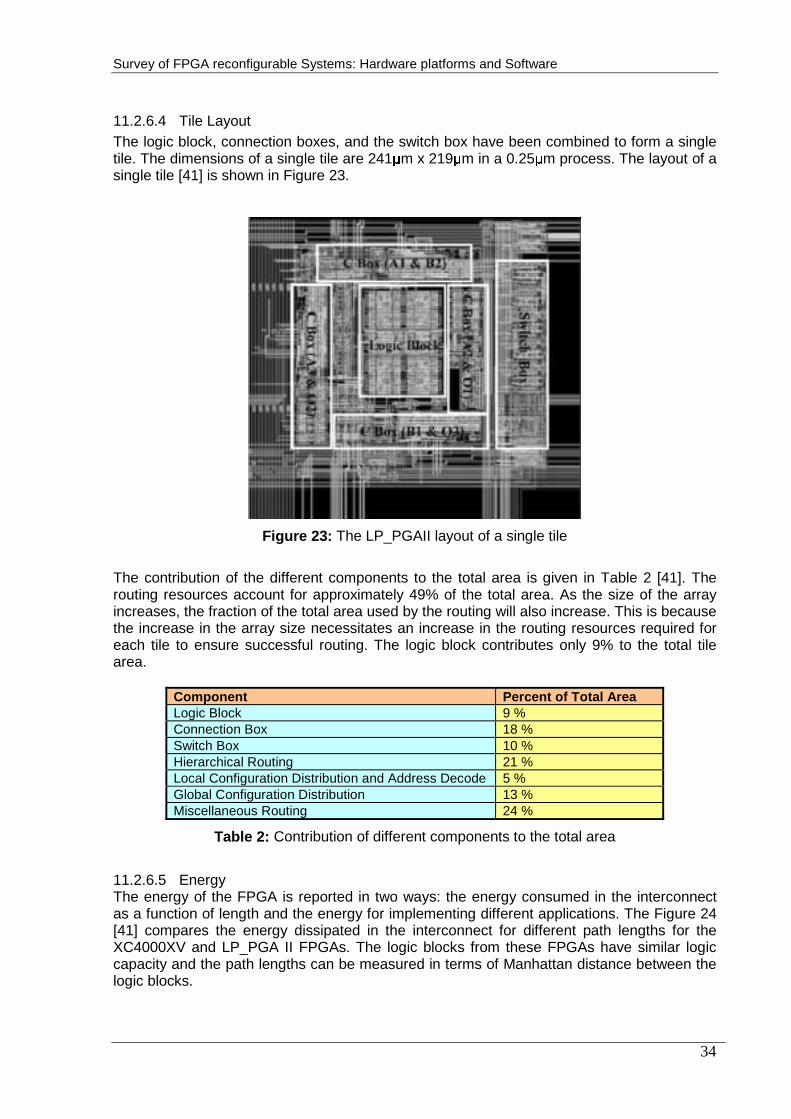
11.2.6.4 Tile Layout The logic block, connection boxes, and the switch box have been combined to form a single tile. The dimensions of a single tile are 241�m x 219�m in a 0.25�m process. The layout of a single tile [41] is shown in Figure 23.
Figure 23: The LP_PGAII layout of a single tile
The contribution of the different components to the total area is given in Table 2 [41]. The routing resources account for approximately 49% of the total area. As the size of the array increases, the fraction of the total area used by the routing will also increase. This is because the increase in the array size necessitates an increase in the routing resources required for each tile to ensure successful routing. The logic block contributes only 9% to the total tile area.
Component Percent of Total Area Logic Block 9 % Connection Box 18 % Switch Box 10 % Hierarchical Routing 21 % Local Configuration Distribution and Address Decode 5 % Global Configuration Distribution 13 % Miscellaneous Routing 24 %
Table 2: Contribution of different components to the total area
11.2.6.5 Energy The energy of the FPGA is reported in two ways: the energy consumed in the interconnect as a function of length and the energy for implementing different applications. The Figure 24 [41] compares the energy dissipated in the interconnect for different path lengths for the XC4000XV and LP_PGA II FPGAs. The logic blocks from these FPGAs have similar logic capacity and the path lengths can be measured in terms of Manhattan distance between the logic blocks.
Survey of FPGA reconfigurable Systems: Hardware platforms and Software
35
���
�
��
���
� � � � �� �� �� �� �� �� �� ��
���� ����� ��������� � �������
��������
���� ����
Figure 24: Energy as a Function of Path Length
In order to explore in more detail the overall energy consumption in the FPGA, a number of applications are mapped onto the array and the energy is measured. The applications are described at the Register Transfer Level, while the mapping to each FPGA is done based on component library for the architecture. The applications are executed with the same data throughput and input data streams. The energy is reported for processing one data token, and it is given in Table 3 [41]. The reported energy is five to sixteen times lower than that of the commercial architecture.
In addition to that, in the same research [41], a comparison of the configuration overhead for programming the Xilinx FPGA and the LP_PGA II is performed. The difference in the configuration energy between the two FPGAs is dramatic, a reduction by three to six orders of magnitude. At the LP_PGAII the energy is a function of the utilization of the array, while the energy is constant for the Xilinx FPGA. The low configuration cost of LP_PGA II makes it a more attractive choice as a performance accelerator. Finally, there is a study of the energy and delay tradeoff. One of the main goals of the LP_PGA II is to minimize the energy while maintaining acceptable speed performance. This resulting in using a 1.5V/0.8V power supply to achieve a maximum toggle frequency of 125MHz. It is possible to run this design at a higher voltage to improve the speed performance. Probably, this improved speed can only be obtained at the cost of higher energy consumption.
11.2.6.6 Configuration Architecture The configuration method used in the low-energy FPGA is that of a random access technique. This makes it possible to selectively program the resources in the FPGA, without having to program the entire array each time.
Survey of FPGA reconfigurable Systems: Hardware platforms and Software
36
11.2.6.7 LP_PGAII Implementation Three prototype FPGAs were built. The first prototype, LP_PGA II, was an array of sixty-four logic blocks. The purpose of this chip was to verify the architectural and circuit techniques aimed at reducing the execution energy. The second prototype was an embedded version of LP_PGA II. The array was used as an accelerator in a digital signal processor for voice band processing. Data obtained from the embedded FPGA verified the applicability of an FPGA in an energy-sensitive platform. This implementation also brought into focus the overhead associated with frequent reconfiguration of the FPGA. The last prototype, LP_PGA II incorporated the improvements to reduce the configuration energy. Measured data from the prototypes demonstrate five times to twenty-two times improvement in execution energy over comparable commercial architectures.
7.2.7. 3D-FPGA 3D-FPGA [42] is a dynamically reconfigurable field programmable gate array (FPGA). The architecture was developed using a methodology that examines different architectural parameters and how they affect different performance criteria such as speed, area, and reconfiguration time. The block diagram of the 3-D FPGA is shown in Figure 25. The resulting architecture has high performance while the requirement of balancing the areas of its constituent layers is satisfied.
Figure 25: Block diagram of the 3-D FPGA
The architecture consists of three layers: the routing and logic block (RLB) layer, the routing layer (RL), and the memory layer (ML). The RLB layer is responsible for implementing logic functions and for performing limited routing. Since it is well known that, for practical applications, most nets are short, it is decided to implement in the RLB layer the portion of the routing structure that will be used for routing short nets. The remaining part of the routing structure is implemented in the RL that is formed by connecting multiple switch boxes in a mesh array structure. The memory layer is used to store configuration bits for both the RLB and routing layers. The number of configuration bits stored in this layer is determined by the size of the RLB and routing layers. The main goal is to achieve a balance between the FPGAs constituent layers. Figure 26 presents the internal structure of the functional unit.
Survey of FPGA reconfigurable Systems: Hardware platforms and Software
37
Figure 26: Internal Structure of the functional unit
A dynamically reconfigurable FPGA must provide a mean of communicating intermediate results between different configuration instantiations. The proposed FPGA allows direct communication between any two configuration instantiations. The SaveS register is provided in order to allow the present state to be saved for subsequent processing. The current state can be loaded into the register when the SaveState signal is enabled. The value of the SaveS register can be retrieved by any configuration instantiation by appropriately setting the value of the RestoreState signal without disturbing the operation of the RLB during the intermediate configuration instantiations. The restored value can be used as one of the inputs into the LUT. The RLBs are organized into clusters. A cluster is formed by a square array of RLBs. The size of the cluster will be determined in Section V-B. Each cluster is associated with a cluster memory block and a switch box in the routing layer. The cluster memory block can be used to store either input data or intermediate results. The size of this cluster memory is dependent upon the mismatch between the areas of the FPGA constituent’s layers.
7.2.8. LEGO The LEGO [43], [44] (Logic that’s Erasable and Greatly Optimized) FPGA basic block is a four-input LUT. The designers’ objective was focused on achieving a high-speed design, while keeping in mind the area tradeoffs. The most critical issues are the design of the switches and minimizing the capacitance of the routing network. The results have shown that the LEGO design compares favorably with existing commercial FPGA’s. Also all the commercial FPGA designs are done using full-custom hand layout to obtain absolute minimum die sizes. This is both labor and time intensive. Here is proposed a design style with a minitile that contains a portion of the components in the logic tile, resulting in less full-custom effort. The minitile is replicated in a 4x4 array to create a macro tile. The minitile is optimized for layout density and speed, and is customized in the array by adding appropriate vias. This technique also permits easy changing of the hard-wired connections in the logic block architecture and the segmentation length distribution in the routing architecture.
7.3. Summary Table 4 provides the main features for some of the above described fine-grain reconfigurable architectures in terms of their programmability, the reconfiguration method, the interface and the possible application domain.
Survey of FPGA reconfigurable Systems: Hardware platforms and Software
38
Table 4: Comparisons of fine-grain academic architectures
8. Commercial fine-grain Reconfigurable platforms This part of the report referred to commercial fine-grain reconfigurable architectures. The best known of them are the FPGAs that various vendors produce. Many FPGA families are described below with figures that show the CLB.
8.1. Xilinx At this part of the document will be described the Spartan, Spartan-XL, Spartan-II, Virtex, Virtex II, and Virtex E family FPGAs.
8.1.1. Spartan and Spartan-XL Families FPGAs The Spartan and the Spartan-XL families [45] are a high-volume production FPGA solution that delivers all the key requirements for ASIC replacement up to 40,000 gates. These requirements include high performance, on-chip RAM, core solutions and prices that, in high volume, approach and in many cases are equivalent to mask programmed ASIC devices. 12.1.1.1 General Overview Spartan series FPGAs are implemented with a regular, flexible, programmable architecture of Configurable Logic Blocks (CLBs), interconnected by a powerful hierarchy of versatile routing resources (routing channels), and surrounded by a perimeter of programmable Input/Output Blocks (IOBs). They have generous routing resources to accommodate the most complex interconnect patterns. The devices are customized by loading configuration data into internal static memory cells. Re-programming is possible an unlimited number of
Survey of FPGA reconfigurable Systems: Hardware platforms and Software
39
times. The values stored in these memory cells determine the logic functions and interconnections implemented in the FPGA. The FPGA can either actively read its configuration data from an external serial PROM (Master Serial mode), or the configuration data can be written into the FPGA from an external device (Slave Serial mode). Spartan series FPGAs can be used where hardware must be adapted to different user applications. 12.1.1.2 Configurable Logic Blocks (CLBs) The Spartan and Spartan-XL CLB elements are composed of three look-up tables (LUT) are used as logic function generators, two flip-flops and two groups of signal steering multiplexers and is shown in Figure 27. Two 16x1 memory look-up table (F-LUT and G-LUT) are used to implement 4-input function generators, each offering unrestricted logic implementation of any Boolean function of up to four independent input signals. Using memory LUT the propagation delay is independent of the function implemented. A third 3-input function generator (H-LUT) can implement any Boolean function of three inputs. The CLB can therefore, implement certain functions of up to nine inputs, like parity checking. The three LUTs in the CLB can also be combined to do any arbitrarily defined Boolean function of five inputs.
12.1.1.3 Routing Channel Description All internal routing channels are composed of metal segments with programmable switching points and switching matrices to implement the desired routing. A structured, hierarchical matrix of routing channels is provided to achieve efficient automated routing. 12.1.1.4 Advanced Features Description • Distributed RAM Optional modes for each CLB allow the function generators (F-LUT and G-LUT) to be used as Random Access Memory (RAM). Read and write operations are significantly faster for this on-chip RAM than for off-chip implementations. This speed advantage is due to the relatively short signal propagation delays within the FPGA. • Fast Carry Logic Each CLB F-LUT and G-LUT contains dedicated arithmetic logic for the fast generation of carry and borrow signals. This extra output is passed on to the function generator in the adjacent CLB. The carry chain is independent of normal routing resources. Dedicated fast carry logic greatly increases the efficiency and performance of adders, subtractors, accumulators, comparators and counters. It also opens the door to many new applications
Survey of FPGA reconfigurable Systems: Hardware platforms and Software
40
involving arithmetic operation, where the previous generations of FPGAs were not fast enough or too inefficient. High-speed address offset calculations in microprocessor or graphics systems, and high-speed addition in digital signal processing, are two typical applications. • 3-State Long Line Drivers A pair of 3-state buffers is associated with each CLB in the array. These 3-state buffers (BUFT) can be used to drive signals onto the nearest horizontal longlines above and below the CLB. They can therefore be used to implement multiplexed or bidirectional buses on the horizontal longlines, saving logic resources. • On-Chip Oscillator Spartan/XL devices include an internal oscillator. This oscillator is used to clock the power-on time-out, for configuration memory clearing, and as the source of CCLK in Master configuration mode. The oscillator runs at a nominal 8 MHz frequency that varies with process, VCC, and temperature. The output frequency falls between 4 MHz and 10 MHz. 12.1.1.5 Configuration Spartan/XL devices use several hundred bits of configuration data per CLB and its associated interconnects. Each configuration bit defines the state of a static memory cell that controls either a function LUT bit, a multiplexer input, or an interconnect pass transistor.
8.1.2. Spartan-II Array The Spartan-II [46] user-programmable gate array is composed of five major configurable elements:
• IOBs provide the interface between the package pins and the internal logic • CLBs provide the functional elements for constructing most logic • Dedicated block RAM memories of 4096 bits each • Clock DLLs for clock-distribution delay compensation and clock domain control • Versatile multi-level interconnect structure
The CLBs form the central logic structure with easy access to all support and routing structures. The IOBs are located around all the logic and memory elements for easy and quick routing of signals on and off the chip. Values stored in static memory cells control all the configurable logic elements and interconnect resources. These values load into the memory cells on power-up, and can reload if necessary to change the function of the device. Each of these elements will be discussed in detail in the following sections. 12.1.2.1 Configurable Logic Block The basic building block of the Spartan-II CLB is the logic cell (LC). An LC includes a 4-input function generator, carry logic, and storage element. Output from the function generator in each LC drives the CLB output and the D input of the flip-flop. Each Spartan-II CLB contains four LCs, organized in two similar slices. In addition to the four basic LCs, the Spartan-II CLB contains logic that combines function generators to provide functions of five or six inputs. Figure 28 shows the identical slices that are placed in each CLB.
Survey of FPGA reconfigurable Systems: Hardware platforms and Software
41
Figure 28: Spartan-II CLB Slice
12.1.2.2 Look-Up Tables Spartan-II function generators are implemented as 4-input LUTs. In addition to operating as a function generator, each LUT can provide a 16 x 1-bit synchronous RAM. Furthermore, the two LUTs within a slice can be combined to create a 16 x 2-bit or 32 x 1-bit synchronous RAM, or a 16 x 1-bit dual-port synchronous RAM. The Spartan-II LUT can also provide a 16-bit shift register that is ideal for capturing high-speed or burst-mode data. This mode can also be used to store data in applications such as DSP. 12.1.2.3 Storage Elements Storage elements in the Spartan-II slice can be configured either as edge-triggered D-type flip-flops or as level-sensitive latches. The D inputs can be driven either by function generators within the slice or directly from slice inputs, bypassing the function generators. 12.1.2.4 Arithmetic Logic Dedicated carry logic provides fast arithmetic carry capability for high-speed arithmetic functions. The Spartan-II CLB supports two separate carry chains, one per slice. The height of the carry chains is two bits per CLB. The arithmetic logic includes an XOR gate that allows a 1-bit full adder to be implemented within an LC. In addition, a dedicated AND gate improves the efficiency of multiplier implementation. The dedicated carry path can also be used to cascade function generators for implementing wide logic functions. 12.1.2.5 Block RAM Spartan-II FPGAs incorporate several large block RAM memories. These complement the distributed RAM LUTs that provide shallow memory structures implemented in CLBs. Block RAM memory blocks are organized in columns. All Spartan-II devices contain two such columns, one along each vertical edge. These columns extend the full height of the chip. Each memory block is four CLBs high, and consequently, a Spartan-II device eight CLBs high will contain two memory blocks per column, and a total of four blocks. 12.1.2.6 Programmable Routing Matrix It is the longest delay path that limits the speed of any worst-case design. Consequently, the Spartan-II routing architecture and its place-and-route software were defined in a single optimization process. This joint optimization minimizes long-path delays, and consequently,
Survey of FPGA reconfigurable Systems: Hardware platforms and Software
42
yields the best system performance. The joint optimization also reduces design compilation times because the architecture is software-friendly. Design cycles are correspondingly reduced due to shorter design iteration times. 12.1.2.7 Configuration Spartan-II devices are configured by sequentially loading frames of data that have been concatenated into a configuration file. It is important to note that, while a PROM is commonly used to store configuration data before loading them into the FPGA, it is by no means required. Any of a number of different kinds of under populated nonvolatile storage already available either on or off the board (i.e., hard drives, FLASH cards, etc.) can be used.
8.1.3. Virtex The Virtex [47] user-programmable gate array, shown in Figure 29, comprises two major configurable elements: the configurable logic blocks (CLBs) which provide the functional elements for constructing logic and input/output blocks (IOBs) that provide the interface between the package pins and the CLBs. The CLBs are interconnected through a general routing matrix (GRM). The GRM comprises an array of routing switches located at the intersections of horizontal and vertical routing channels. Each CLB nests into a VersaBlock that also provides local routing resources to connect the CLB to the GRM. The VersaRing I/O interface provides additional routing resources around the periphery of the device. This routing improves I/O routability and facilitates pin locking. The Virtex architecture also includes the following circuits that connect to the GRM.
• Dedicated block memories of 4096 bits each. • Clock DLLs for clock-distribution delay compensation and clock domain control. • 3-State buffers (BUFTs) associated with each CLB that drive dedicated segmentable
horizontal routing resources.
Values stored in static memory cells control the configurable logic elements and interconnect resources. These values load into the memory cells on power-up, and can reload if necessary to change the function of the device.
Figure 29: Virtex architecture overview
12.1.3.1 Configurable Logic Block The basic building block of the Virtex CLB is the logic cell (LC). An LC includes a 4-input function generator, carry logic, and a storage element. The output from the function generator in each LC drives both the CLB output and the D input of the flip-flop. Each Virtex CLB contains four LCs, organized in two similar slices, as shown in Figure 30.
Survey of FPGA reconfigurable Systems: Hardware platforms and Software
43
Figure 30: A 2-Slice Virtex CLB
In addition to the four basic LCs, the Virtex CLB contains logic that combines function generators to provide functions of five or six inputs. Consequently, when estimating the number of system gates provided by a given device, each CLB counts as 4.5 LCs. 12.1.3.2 Look-Up Tables Virtex function generators are implemented as 4-input LUTs. In addition to operating as a function generator, each LUT can provide a 16 x 1-bit synchronous RAM. Furthermore, the two LUTs within a slice can be combined to create a 16 x 2-bit or 32 x 1-bit synchronous RAM, or a 16x1-bit dual-port synchronous RAM. The Virtex LUT can also provide a 16-bit shift register that is ideal for capturing high-speed or burst-mode data. This mode can also be used to store data in applications such as Digital Signal Processing. 12.1.3.3 Storage Elements The storage elements in the Virtex slice can be configured either as edge-triggered D-type flip-flops or as level-sensitive latches. The D inputs can be driven either by the function generators within the slice or directly from slice inputs, bypassing the function generators. In addition to Clock and Clock Enable signals, each Slice has synchronous set and reset signals (SR and BY). SR forces a storage element into the initialization state specified for it in the configuration. The BY forces it into the opposite state. Alternatively, these signals can be configured to operate asynchronously. All of the control signals are independently invertible, and are shared by the two flip-flops within the slice. 12.1.3.4 Arithmetic Logic Dedicated carry logic provides fast arithmetic carry capability for high-speed arithmetic functions. The Virtex CLB supports two separate carry chains, one per Slice. The height of the carry chains is two bits per CLB. The arithmetic logic includes an XOR gate that allows a 1-bit full adder to be implemented within an LC. In addition, a dedicated AND gate improves the efficiency of multiplier implementation. The dedicated carry path can also be used to cascade function generators for implementing wide logic functions. 12.1.3.5 Block SelectRAM Virtex FPGAs incorporate several large Block SelectRAM memories. These complement the distributed LUT SelectRAMs that provide shallow RAM structures implemented in CLBs. The SelectRAM memory blocks are organized in columns. All Virtex devices contain two such columns, one along each vertical edge. These columns extend the full height of the chip. Each memory block is four CLBs high, and consequently, a Virtex device 64 CLBs high contains 16 memory blocks per column, and a total of 32 blocks. The Virtex Block
Survey of FPGA reconfigurable Systems: Hardware platforms and Software
44
SelectRAM also includes dedicated routing to provide an efficient interface with both CLBs and other Block SelectRAMs. 12.1.3.6 Programmable Routing Matrix It is the longest delay path that limits the speed of any worst-case design. Consequently, the Virtex routing architecture and its place-and-route software were defined in a single optimization process. This joint optimization minimizes long-path delays, and consequently, yields the best system performance. The joint optimization also reduces design compilation times because the architecture is software-friendly. Design cycles are correspondingly reduced due to shorter design iteration times. 12.1.3.7 Configuration Virtex devices are configured by loading configuration data into the internal configuration memory. Some of the pins used for this are dedicated configuration pins, while others can be re-used as general-purpose inputs and outputs once configuration is complete. Multiple FPGAs can be daisy-chained for configuration from a single source.
12.1.4 Virtex-E The Virtex-E FPGA family [93] delivers high-performance, high-capacity programmable logic solutions. Dramatic increases in silicon efficiency result from optimizing the new architecture for place-and-route efficiency and exploiting an aggressive 6-����� ����� �� �� ���process. These advances make Virtex-E FPGAs powerful and flexible alternatives to mask-programmed gate arrays. The Virtex-E family includes the nine members. Combining a wide variety of programmable system features, a rich hierarchy of fast, flexible interconnect resources, and advanced process technology, the Virtex-E family delivers a high-speed and high-capacity programmable logic solution that enhances design flexibility while reducing time-to-market. 12.1.4.1 Architecture Virtex-E devices feature a flexible, regular architecture that comprises an array of configurable logic blocks (CLBs) surrounded by programmable input/output blocks (IOBs), all interconnected by a rich hierarchy of fast, versatile routing resources. The abundance of routing resources permits the Virtex-E family to accommodate even the largest and most complex designs. Virtex-E FPGAs are SRAM-based, and are customized by loading configuration data into internal memory cells. 12.1.4.2 Virtex-E Array The Virtex-E user-programmable gate array, shown in Figure 31, comprises two major configurable elements: configurable logic blocks (CLBs) which provide the functional elements for constructing logic, and input/output blocks (IOBs) that provide the interface between the package pins and the CLBs. The CLBs are interconnected through a general routing matrix (GRM), which comprises an array of routing switches located at the intersections of horizontal and vertical routing channels. Each CLB nests into a VersaBlock that also provides local routing resources to connect the CLB to the GRM.
Survey of FPGA reconfigurable Systems: Hardware platforms and Software
45
Figure 31: Virtex-E Architecture Overview
The VersaRing I/O interface provides additional routing resources around the periphery of the device. This routing improves I/O routability and facilitates pin locking. The Virtex-E architecture also includes the following circuits that connect to the GRM:
• Dedicated block memories of 4096 bits each. • Clock DLLs for clock-distribution delay compensation and clock domain control. • 3-State buffers (BUFTs) associated with each CLB that drive dedicated segmentable
horizontal routing resources. Values stored in static memory cells control the configurable logic elements and interconnect resources. These values load into the memory cells on power-up, and can reload if necessary to change the function of the device. 12.1.4.3 Configurable Logic Blocks The basic building block of the Virtex-E CLB is the logic cell (LC). An LC includes a 4-input function generator, carry logic, and a storage element. The output from the function generator in each LC drives both the CLB output and the D input of the flip-flop. Each Virtex-E CLB contains four LCs, organized in two similar slices, as have been shown in Figure 30. In addition to the four basic LCs, the Virtex-E CLB contains logic that combines function generators to provide functions of five or six inputs. Consequently, when estimating the number of system gates provided by a given device, each CLB counts as 4.5 LCs. 12.1.4.4 Look-Up Tables Virtex-E function generators are implemented as 4-input LUTs. In addition to operating as a function generator, each LUT can provide a 16x1-bit synchronous RAM. Furthermore, the two LUTs within a slice can be combined to create a 16x2-bit or 32x1-bit synchronous RAM, or a 16x1-bit dual-port synchronous RAM. The Virtex-E LUT can also provide a 16-bit shift register that is ideal for capturing high-speed or burst-mode data. This mode can also be used to store data in applications such as Digital Signal Processing. 12.1.4.5 Virtex-E Compared to Virtex Devices The Virtex-E family offers up to 43,200 logic cells in devices up to 30% faster than the Virtex family. I/O performance is increased to 622 Mb/s using Source Synchronous data transmission architectures and synchronous system performance up to 240 MHz using singled-ended SelectI/O technology. Additional I/O standards are supported, notably LVPECL, LVDS, and BLVDS, which use two pins per signal. Almost all signal pins can be used for these new standards.
Survey of FPGA reconfigurable Systems: Hardware platforms and Software
46
Virtex-E devices have up to 640 Kb of faster (250 MHz) block SelectRAM, but the individual RAMs are the same size and structure as in the Virtex family. They also have eight DLLs instead of the four in Virtex devices. Each individual DLL is slightly improved with easier clock mirroring and 4x frequency multiplication. The supply voltage for the internal logic and memory, is 1.8 V, instead of 2.5 V for Virtex devices. Advanced processin� ��� �� ��design rules have resulted in smaller dice, faster speed, and lower power consumption. The Virtex-E family is not bitstream-compatible with the Virtex family, but Virtex designs can be compiled into equivalent Virtex-E devices. The same device in the same package for the Virtex-E and Virtex families are pin-compatible with some minor exceptions.
12.1.5 Virtex-II The Virtex-II family [94] is a platform FPGA developed for high performance from low-density to high-density designs that are based on IP cores and customized modules. The family delivers complete solutions for telecommunication, wireless, networking, video, and DSP applications, including PCI, LVDS, and DDR interfaces. The leading-edge 0.15 µm / 0.12 µm CMOS 8-layer metal process and the Virtex-II architecture are optimized for high speed with low power consumption. Combining a wide variety of flexible features and a large range of densities up to 10 million system gates, the Virtex-II family enhances programmable logic design capabilities and is a powerful alternative to mask-programmed gates arrays. The Virtex-II family comprises 11 members, ranging from 40K to 8M system gates. 12.1.5.1 Array Architecture Overview Virtex-II devices are user-programmable gate arrays with various configurable elements. As shown in Figure 32, the programmable device is comprised of input/output blocks (IOBs) and internal configurable logic blocks (CLBs).
Figure 32: Virtex-II Architecture Overview
Survey of FPGA reconfigurable Systems: Hardware platforms and Software
47
The internal configurable logic includes four major elements organized in a regular array. Those are:
• Configurable Logic Blocks (CLBs) provide functional elements for combinatorial and synchronous logic, including basic storage elements. BUFTs (3-state buffers) associated with each CLB element drive dedicated segmentable horizontal routing resources.
• Block SelectRAM memory modules provide large 18 Kbit storage elements of dual-port RAM.
• Multiplier blocks are 18-bit x 18-bit dedicated multipliers. • DCM (Digital Clock Manager) blocks provide self-calibrating, fully digital solutions for
clock distribution delay compensation, clock multiplication and division, coarse- and fine-grained clock phase shifting.
12.1.5.2 Configurable Logic Blocks The Virtex-II configurable logic blocks (CLB) are organized in an array and are used to build combinatorial and synchronous logic designs. The CLB resources include four slices and two 3-state buffers. Each slice is equivalent and contains:
• Two function generators (F & G) • Two storage elements • Arithmetic logic gates • Large multiplexers • Wide function capability • Fast carry look-ahead chain • Horizontal cascade chain (OR gate)
The function generators F & G are configurable as 4-input LUTs, as 16-bit shift registers, or as 16-bit distributed SelectRAM memory. In addition, the two storage elements are either edge-triggered D-type flip-flops or level-sensitive latches. Each CLB has internal fast interconnect and connects to a switch matrix to access general routing resources. 12.1.5.3 Slice Description Each slice includes two 4-input function generators, carry logic, arithmetic logic gates, wide function multiplexers and two storage elements. Each 4-input function generator is programmable as a 4-input LUT, 16 bits of distributed SelectRAM memory, or a 16-bit variable- tap shift register element, and each of them are capable of implementing any arbitrarily defined Boolean function of four inputs.. The output from the function generator in each slice drives both the slice output and the D input of the storage element. 12.1.5.4 Configuration Virtex-II devices are configured by loading application specific configuration data into the internal configuration memory. Configuration is carried out using a subset of the device pins, some of which are dedicated, while others can be re-used as general purpose inputs and outputs once configuration is complete. One of the major advantages of Virtex-II devices is their ability for the partial reconfiguration. With this technique, instead of resetting the chip and doing a full configuration, new data is loaded into a specified area of the chip, while the rest of the chip remains in operation. Data is loaded on a column basis, with the smallest load unit being a configuration “frame” of the bitstream (device size dependent). Partial reconfiguration is useful for applications that require different designs to be loaded into the same area of a chip, or that require the ability to change portions of a design without having to reset or reconfigure the entire chip.
Survey of FPGA reconfigurable Systems: Hardware platforms and Software
48
8.2. ALTERA The Startix, Apex_II, APEX 20KC, Mercury, FLEX 10KC, ACEX 1K, and FLEX 6000 FPGA families are described at this part of the document.
8.2.1. Startix The Stratix family [48] of programmable logic devices (PLDs) is based on a 1.5-V, 0.13-µm, all-layer copper SRAM process, with densities up to 114,140 logic elements (LEs) and up to 10 Mbits of RAM. Stratix devices offer up to 28 digital signal processing (DSP) blocks with up to 224 (9-bit x ��-bit) embedded multipliers, optimized for DSP applications that enable efficient implementation of high-performance filters and multipliers. Stratix devices support various I/O standards and also offer a complete clock management solution with its hierarchical clock structure with up to 420-MHz performance and up to 12 phase-locked loops (PLLs). 12.2.1.1 Functional Description Stratix devices contain a two-dimensional row- and column-based architecture to implement custom logic. A series of column and row interconnects of varying length and speed provides signal interconnection between logic array blocks (LABs), memory block structures, and DSP blocks. The logic array consists of LABs, with 10 logic elements (LEs) in each LAB. An LE is a small unit of logic providing efficient implementation of user logic functions. LABs are grouped into rows and columns across the device. M512 RAM blocks are simple dual-port memory blocks with 512 bits plus parity (576 bits). These blocks provide dedicated simple dual-port or single-port memory up to 18-bits wide at up to 312 MHz. M512 blocks are grouped into columns across the device in between certain LABs. 12.2.1.2 Logic Array Blocks Each LAB consists of 10 LEs, LE carry chains, LAB control signals, local interconnect, LUT chain, and register chain connection lines. The local interconnect transfers signals between LEs in the same LAB. LUT chain connections transfer the output of one LE’s LUT to the adjacent LE for fast sequential LUT connections within the same LAB. Register chain connections transfer the output of one LE’s register to the adjacent LE’s register within an LAB. The Quartus II Compiler places associated logic within an LAB or adjacent LABs, allowing the use of local, LUT chain, and register chain connections for performance and area efficiency. 12.2.1.3 LAB Interconnects The LAB local interconnect can drive LEs within the same LAB. The LAB local interconnect is driven by column and row interconnects and LE outputs within the same LAB. Neighboring LABs, M512 RAM blocks, M4K RAM blocks, or DSP blocks from the left and right can also drive an LAB’s local interconnect through the direct link connection. The direct link connection feature minimizes the use of row and column interconnects, providing higher performance and flexibility. Each LE can drive 30 other LEs through fast local and direct link interconnects. 12.2.1.4 Logic Elements The smallest unit of logic in the Stratix architecture, the LE, is compact and provides advanced features with efficient logic utilization. Each LE contains a four-input LUT, which is a function generator that can implement any function of four variables. In addition, each LE contains a programmable register and carry chain with carry select capability. A single LE also supports dynamic single bit addition or subtraction mode selectable by an LAB-wide control signal. Each LE drives all types of interconnects: local, row, column, LUT chain, register chain, and direct link interconnects. The Startix logic element schematic is shown in Figure 33.
Survey of FPGA reconfigurable Systems: Hardware platforms and Software
49
Figure 33: Startix Logic Element
Each LE has three outputs that drive the local, row, and column routing resources. The LUT or register output can drive these three outputs independently. Two LE outputs drive column or row and direct link routing connections and one drives local interconnect resources. This allows the LUT to drive one output while the register drives another output. This feature, called register packing, improves device utilization because the device can use the register and the LUT for unrelated functions. Another special packing mode allows the register output to feed back into the LUT of the same LE so that the register is packed with its own fan-out LUT. This provides another mechanism for improved fitting. The LE can also drive out registered and unregistered versions of the LUT output. 12.2.1.5 MultiTrack Interconnect In the Stratix architecture, connections between LEs, TriMatrix memory, DSP blocks, and device I/O pins are provided by the MultiTrack interconnect structure with DirectDrive technology. The MultiTrack interconnect consists of continuous, performance-optimized routing lines of different lengths and speeds used for inter- and intra-design block connectivity. The Quartus II Compiler automatically places critical design paths on faster interconnects to improve design performance. 12.2.1.6 TriMatrix Memory TriMatrix memory consists of three types of RAM blocks: M512, M4K, and MegaRAM blocks. Although these memory blocks are different, they can all implement various types of memory with or without parity, including true dual-port, simple dual-port, and single-port RAM, ROM, and FIFO buffers. 12.2.1.7 Digital Signal Processing Block The most commonly used DSP functions are finite impulse response (FIR) filters, complex FIR filters, infinite impulse response (IIR) filters, fast Fourier transform (FFT) functions, direct cosine transform (DCT) functions, and correlators. All of these blocks have the same fundamental building block: the multiplier. Additionally, some applications need specialized operations such as multiply-add and multiply-accumulate operations. Stratix devices provide
Survey of FPGA reconfigurable Systems: Hardware platforms and Software
50
DSP blocks to meet the arithmetic requirements of these functions. Each Stratix device has two columns of DSP blocks to efficiently implement DSP functions faster than LE-based implementations. Larger Stratix devices have more DSP blocks per column. 12.2.1.8 Configuration The logic, circuitry, and interconnects in the Stratix architecture are configured with CMOS SRAM elements. Stratix devices can be configured on the board for the specific functionality required. In addition to that, they can be configured at system power-up with data stored in an Altera serial configuration device or provided by a system controller. The Stratix device’s optimized interface allows microprocessors to configure it serially or in parallel, and synchronously or asynchronously. The interface also enables microprocessors to treat Stratix devices as memory and configure them by writing to a virtual memory location, making reconfiguration easy. After a Stratix device has been configured, it can be reconfigured in-circuit by resetting the device and loading new data. Real-time changes can be made during system operation, enabling innovative reconfigurable computing applications. 12.2.1.9 Software Stratix devices are supported by the Altera Quartus II design software, which provides a comprehensive environment for system-on-programmable-chip (SOPC) design. The Quartus II software includes HDL and schematic design entry, compilation and logic synthesis, full simulation and advanced timing analysis, SignalTap logic analysis, and device configuration.
8.2.2. Apex_II APEX II devices [49] incorporate LUT-based logic, product-term-based logic, memory, and high-speed I/O standards into one device. Signal interconnections within APEX II devices (as well as to and from device pins) are provided by the FastTrack interconnect, which is a series of fast, continuous row and column channels that run the entire length and width of the device. 12.2.2.1 MegaLAB Structure APEX II devices are constructed from a series of MegaLAB structures. Each MegaLAB structure contains a group of logic array blocks (LABs), one ESB, and a MegaLAB interconnect, which routes signals within the MegaLAB structure. Signals are routed between MegaLAB structures and I/O pins via the FastTrack interconnect. In addition, the edge LABs can be driven by I/O pins through the local interconnect. 12.2.2.2 Logic Array Block Each LAB consists of 10 LEs, the LEs’ associated carry and cascade chains, LAB control signals, and the local interconnect. The local interconnect transfers signals between LEs in the same or adjacent LABs, IOEs, or ESBs. The Quartus II Compiler places associated logic within a LAB or adjacent LABs, allowing the use of a fast local interconnect for high performance. APEX II devices use an interleaved LAB structure, so that each LAB can drive two local interconnect areas. Every other LE drives to either the left or right local interconnect area, alternating by LE. The local interconnect can drive LEs within the same LAB or adjacent LABs. This feature minimizes the use of the row and column interconnects, providing higher performance and flexibility. Each LAB structure can drive 30 LEs through fast local interconnects. 12.2.2.3 Logic Element The LE is the smallest unit of logic in the APEX II architecture. Each LE contains a four-input LUT, which is a function generator that can quickly implement any function of four variables. In addition, each LE contains a programmable register and carry and cascade chains. Each LE drives the local interconnect, MegaLAB interconnect, and FastTrack interconnect routing structures. The Figure 34 shows the logic element of Apex_II, which is similar to Startix FPGA.
Survey of FPGA reconfigurable Systems: Hardware platforms and Software
51
Figure 34: Apex_II Logic Element
Each LE’s programmable register can be configured for D, T, JK, or SR operation. The register’s clock and clear control signals can be driven by global signals, general-purpose I/O pins, or any internal logic. For combinatorial functions, the register is bypassed and the output of the LUT drives the outputs of the LE. Each LE has two outputs that drive the local, MegaLAB, or FastTrack interconnect routing structure. Each output can be driven independently by the LUT’s or register’s output. This feature, called register packing, improves device utilization because the register and the LUT can be used for unrelated functions. The LE can also drive out registered and unregistered versions of the LUT output. The APEX II architecture provides two types of dedicated high-speed data paths that connect adjacent LEs without using local interconnect paths: carry chains and cascade chains. A carry chain supports high-speed arithmetic functions such as counters and adders, while a cascade chain implements wide-input functions such as equality comparators with minimum delay. Carry and cascade chains connect LEs 1 through 10 in an LAB and all LABs in the same MegaLAB structure. 12.2.2.4 Carry Chain The carry chain provides a fast carry-forward function between LEs. The carry-in signal from a lower-order bit drives forward into the higher-order bit via the carry chain, and feeds into both the LUT and the next portion of the carry chain. This feature allows the APEX II architecture to implement high-speed counters, adders, and comparators of arbitrary width. The Quartus II Compiler can create carry chain logic automatically during the design process, or the designer can create it manually during design entry. The Quartus II Compiler creates carry chains longer than 10 LEs by linking LABs together automatically. For enhanced fitting, a long carry chain skips alternate LABs in a MegaLAB structure. A carry chain longer than one LAB skips either from an even-numbered LAB to the next even-numbered LAB, or from an odd-numbered LAB to the next odd-numbered LAB.
Survey of FPGA reconfigurable Systems: Hardware platforms and Software
52
12.2.2.5 Cascade Chain With the cascade chain, the APEX II architecture can implement functions with a very wide fan-in. Adjacent LUTs can compute portions of a function in parallel; the cascade chain serially connects the intermediate values. The cascade chain can use a logical AND or logical OR to connect the outputs of adjacent LEs. Each additional LE provides four more inputs to the effective width of a function, with a short cascade delay. The Quartus II Compiler can create cascade chain logic automatically during the design process, or the designer can create it manually during design entry. Cascade chains longer than 10 LEs are implemented automatically by linking LABs together. For enhanced fitting, a long cascade chain skips alternate LABs in a MegaLAB structure. A cascade chain longer than one LAB skips either from an even-numbered LAB to the next even-numbered LAB, or from an odd-numbered LAB to the next odd-numbered LAB. 12.2.2.6 FastTrack Interconnect In the APEX II architecture, connections between LEs, ESBs, and I/O pins are provided by the FastTrack interconnect. The FastTrack interconnect is a series of continuous horizontal and vertical routing channels that traverse the device. This global routing structure provides predictable performance, even in complex designs. In contrast, the segmented routing in FPGAs requires switch matrices to connect a variable number of routing paths, increasing the delays between logic resources and reducing performance. 12.2.2.7 Software APEX II devices are supported by the Altera Quartus II development system: a single, integrated package that offers hardware description language (HDL) and schematic design entry, compilation and logic synthesis, full simulation and worst-case timing analysis, SignalTap logic analysis, and device configuration. The Quartus II software includes the LogicLock incremental design feature. The LogicLock feature allows the designer to make pin and timing assignments, verify functionality and performance, and then set constraints to lock down the placement and performance of a specific block of logic using LogicLock constraints. 12.2.2.8 Configuration The logic, circuitry, and interconnects in the APEX II architecture are configured with CMOS SRAM elements. APEX II devices are configured at system power-up with data either stored in an Altera configuration device or provided by a system controller. Altera offers in-system programmability (ISP)-capable configuration devices, which configure APEX II devices via a serial data stream. Moreover, APEX II devices contain an optimized interface that permits microprocessors to configure APEX II devices serially or in parallel, synchronously or asynchronously. This interface also enables microprocessors to treat APEX II devices as memory and to configure the device by writing to a virtual memory location, simplifying reconfiguration.
8.2.3. APEX 20KC Similar to APEX 20K and APEX 20KE devices, APEX 20KC devices [50] offer the MultiCore architecture, which combines the strengths of LUT-based and product-term-based devices with an enhanced memory structure. LUT-based logic provides optimized performance and efficiency for datapath, register-intensive, mathematical, or digital signal processing (DSP) designs. Product-term-based logic is optimized for complex combinatorial paths, such as complex state machines. 12.2.3.1 Functional Description APEX 20KC devices incorporate LUT-based logic, product-term-based logic, and memory into one device on an all-copper technology process. Signal interconnections within APEX 20KC devices (as well as to and from device pins) are provided by the FastTrack
Survey of FPGA reconfigurable Systems: Hardware platforms and Software
53
interconnect, which is a series of fast, continuous row and column channels that run the entire length and width of the device. 12.2.3.2 MegaLAB Structure APEX 20KC devices are constructed from a series of MegaLAB structures. Each MegaLAB structure contains 16 logic array blocks (LABs), one ESB, and a MegaLAB interconnect, which routes signals within the MegaLAB structure. In EP20K1000C devices, MegaLAB structures contain 24 LABs. Signals are routed between MegaLAB structures and I/O pins via the FastTrack interconnect. In addition, edge LABs can be driven by I/O pins through the local interconnect. 12.2.3.3 Logic Array Block Each LAB consists of 10 LEs, the LEs’ associated carry and cascade chains, LAB control signals, and the local interconnect. The local interconnect transfers signals between LEs in the same or adjacent LABs, IOEs, or ESBs. The Quartus II Compiler places associated logic within an LAB or adjacent LABs, allowing the use of a fast local interconnect for high performance. APEX 20KC devices use an interleaved LAB structure. This structure allows each LE to drive two local interconnect areas, minimizing the use of the MegaLAB and FastTrack interconnect and providing higher performance and flexibility. Each LE can drive 29 other LEs through the fast local interconnect. 12.2.3.4 Logic Element The LE, the smallest unit of logic in the APEX 20KC architecture, is compact and provides efficient logic usage. Each LE contains a four-input LUT, which is a function generator that can quickly implement any function of four variables. In addition, each LE contains a programmable register and carry and cascade chains. The CLB element is similar to Startix FPGA and it has been shown in Figure 33. Each LE’s programmable register can be configured for D, T, JK, or SR operation. The register’s clock and clear control signals can be driven by global signals, general-purpose I/O pins, or any internal logic. For combinatorial functions, the register is bypassed and the output of the LUT drives the outputs of the LE. Every LE has two outputs that drive the local, MegaLAB, or FastTrack interconnect routing structure. Each output can be driven independently by the LUT’s or register’s output. This feature, called register packing, improves device utilization because the register and the LUT can be used for unrelated functions. The LE can also drive out registered and unregistered versions of the LUT output.
8.2.4. Mercury The Mercury architecture [51] contains a row-based logic array to implement general logic and a row-based embedded system array to implement memory and specialized logic functions. Signal interconnections within Mercury devices are provided by a series of row and column interconnects with varying lengths and speeds. The priority FastTrack Interconnect structure is faster than other interconnects. 12.2.4.1 Logic and Interconnect Mercury device logic is implemented in LEs. LE resources are used differently according to specific operating modes and the type of logic function being implemented. LEs are grouped into LABs in a row-based architecture. The multi-level FastTrack Interconnect structure provides the routing connection between LEs, ESBs, and IOEs. 12.2.4.2 Logic Array Block Each Logic Array Block (LAB) consists of 10 LEs, LE carry chains, multiplier circuitry, LAB control signals, local interconnect, and FastLUT connection lines. The local interconnect transfers signals between LEs within the same or adjacent LABs. FastLUT connections transfer the output of one LE to the adjacent LE for ultra-fast sequential LE connections
Survey of FPGA reconfigurable Systems: Hardware platforms and Software
54
within the same LAB. The Quartus II Compiler places associated logic within a LAB or adjacent LABs, allowing the use of fast local and FastLUT connections for high performance. Mercury devices use an interleaved LAB structure, which allows each LAB to drive two local interconnect areas. Every other LE drives to either the left or right local interconnect area, alternating by LE. The local interconnect can drive LEs within the same LAB or adjacent LABs. This feature minimizes use of the row and column interconnects, providing higher performance and flexibility. Each LAB structure can drive 30 LEs through fast local interconnects. 12.2.4.3 Logic Element The LE, the smallest unit of logic in the Mercury architecture, is compact and provides efficient logic usage and it is shown in Figure 35. Each LE contains a 4-input LUT, which is a function generator that can quickly implement any function of four variables. In addition, each LE contains a programmable register and carry chain with carry select look ahead capability. Each LE also has the ability to drive its combinatorial output directly to the next LE in the LAB. The LE’s programmable register can be configured for D, T, JK, or SR operation.
Figure 35: Mercury Logic Element
12.2.4.4 FastLUT Interconnect Mercury devices include an enhanced interconnect structure within LABs for faster routing of LE output to LE input connections. The FastLUT connection allows the combinatorial output of an LE to directly drive the fast input of the LE directly below it, bypassing the local interconnect. This resource can be used as a high speed connection for wide fan-in functions from LE 1 to LE 10 in the same LAB. 12.2.4.5 Configuration The logic, circuitry, and interconnects in the Mercury architecture are configured with CMOS SRAM elements. Mercury devices are reconfigurable and as a result, test vectors do not have to be generated for fault coverage purposes. Instead, the designer can focus on simulation and design verification. Mercury devices can be configured on the board for the specific functionality required. They are configured at system power-up with data stored in an Altera serial configuration device or provided by a system controller. Altera offers in-system programmability (ISP)-capable configuration devices, which configure Mercury devices via a
Survey of FPGA reconfigurable Systems: Hardware platforms and Software
55
serial data stream. Mercury devices contain an optimized interface that permits microprocessors to configure devices serially or in parallel, synchronously or asynchronously. This interface also enables microprocessors to treat Mercury devices as memory and to configure the device by writing to a virtual memory location, simplifying reconfiguration. After a Mercury device has been configured, it can be reconfigured in-circuit by resetting the device and loading new data. Real-time changes can be made during system operation, enabling innovative reconfigurable computing applications.
8.2.5. FLEX 10K Altera’s FLEX 10K devices [52] are based on reconfigurable CMOS SRAM elements, the Flexible Logic Element MatriX (FLEX) architecture incorporates all features necessary to implement common gate array mega-functions. With up to 250,000 gates, the FLEX 10K family provides the density, speed, and features to integrate entire systems, including multiple 32-bit buses, into a single device. 12.2.5.1 Architecture The FLEX 10K architecture is similar to that of embedded gate arrays. As with standard gate arrays, embedded gate arrays implement general logic in a conventional “sea-of-gates” architecture. In addition, embedded gate arrays have dedicated die areas for implementing large, specialized functions. By embedding functions in silicon, embedded gate arrays provide reduced die area and increased speed compared to standard gate arrays. However, embedded mega-functions typically cannot be customized, limiting the designer’s options. In contrast, FLEX 10K devices are programmable, providing the designer with full control over embedded mega-functions and general logic while facilitating iterative design changes during debugging. Each FLEX 10K device contains an embedded array and a logic array. The embedded array is used to implement a variety of memory functions or complex logic functions, such as digital signal processing (DSP), microcontroller, wide-data-path manipulation, and data-transformation functions. The logic array performs the same function as the sea-of-gates in the gate array: it is used to implement general logic, such as counters, adders, state machines, and multiplexers. The combination of embedded and logic arrays provides the high performance and high density of embedded gate arrays, enabling designers to implement an entire system on a single device. 12.2.5.2 Functional Description Each FLEX 10K device contains an embedded array to implement memory and specialized logic functions, and a logic array to implement general logic. The embedded array consists of a series of EABs. When implementing memory functions, each EAB provides 2,048 bits, which can be used to create RAM, ROM, dual-port RAM, or first-in first-out (FIFO) functions. When implementing logic, each EAB can contribute 100 to 600 gates towards complex logic functions, such as multipliers, microcontrollers, state machines, and DSP functions. EABs can be used independently, or multiple EABs can be combined to implement larger functions. The logic array consists of logic array blocks (LABs). Each LAB contains eight LEs and a local interconnect. An LE consists of a 4-input LUT, a programmable flip-flop, and dedicated signal paths for carry and cascade functions. The eight LEs can be used to create medium-sized blocks of logic or combined across LABs to create larger logic blocks. Each LAB represents about 96 usable gates of logic. 12.2.5.3 Embedded Array Block The Embedded Array Block (EAB) is a flexible block of RAM with registers on the input and output ports, and is used to implement common gate array mega-functions. The EAB is also suitable for functions such as multipliers, vector scalars, and error correction circuits, because it is large and flexible. These functions can be combined in applications such as digital filters and microcontrollers. Logic functions are implemented by programming the EAB
Survey of FPGA reconfigurable Systems: Hardware platforms and Software
56
with a read-only pattern during configuration, creating a large LUT. With LUTs, combinatorial functions are implemented by looking up the results, rather than by computing them. This implementation of combinatorial functions can be faster than using algorithms implemented in general logic, a performance advantage that is further enhanced by the fast access times of EABs. The large capacity of EABs enables designers to implement complex functions in one logic level without the routing delays associated with linked LEs or FPGA RAM blocks. The EAB provides advantages over FPGAs, which implement on-board RAM as arrays of small, distributed RAM blocks. These FPGA RAM blocks contain delays that are less predictable as the size of the RAM increases. In addition, FPGA RAM blocks are prone to routing problems because small blocks of RAM must be connected together to make larger blocks. In contrast, EABs can be used to implement large, dedicated blocks of RAM that eliminate these timing and routing concerns. 12.2.5.4 Logic Array Block Each LAB consists of eight LEs, their associated carry and cascade chains, LAB control signals, and the LAB local interconnect. The LAB provides the coarse-grained structure to the FLEX 10K architecture, facilitating efficient routing with optimum device utilization and high performance. 12.2.5.5 Logic Element The LE, the smallest unit of logic in the FLEX 10K architecture, has a compact size that provides efficient logic utilization. Each LE contains a four-input LUT, which is a function generator that can quickly compute any function of four variables. In addition, each LE contains a programmable flip-flop with a synchronous enable, a carry chain, and a cascade chain. Each LE drives both the local and the FastTrack Interconnect. See Figure 36.
Figure 36: FLEX 10K Logic Element
The programmable flip-flop in the LE can be configured for D, T, JK, or SR operation. The clock, clear, and preset control signals on the flip-flop can be driven by global signals, general-purpose I/O pins, or any internal logic. For combinatorial functions, the flip-flop is bypassed and the output of the LUT drives the output of the LE. The LE has two outputs that drive the interconnect; one drives the local interconnect and the other drives either the row or column FastTrack Interconnect. The two outputs can be controlled independently. This feature, called register packing, can improve LE utilization because the register and the LUT
Survey of FPGA reconfigurable Systems: Hardware platforms and Software
57
can be used for unrelated functions. The FLEX 10K architecture provides two types of dedicated high-speed data paths that connect adjacent LEs without using local interconnect paths: carry chains and cascade chains. The carry chain supports high-speed counters and adders; the cascade chain implements wide-input functions with minimum delay. Carry and cascade chains connect all LEs in an LAB and all LABs in the same row. Intensive use of carry and cascade chains can reduce routing flexibility. Therefore, the use of these chains should be limited to speed-critical portions of a design. 12.2.5.6 FastTrack Interconnect In the FLEX 10K architecture, connections between LEs and device I/O pins are provided by the FastTrack Interconnect, which is a series of continuous horizontal and vertical routing channels that traverse the device. This global routing structure provides predictable performance, even in complex designs. In contrast, the segmented routing in FPGAs requires switch matrices to connect a variable number of routing paths, increasing the delays between logic resources and reducing performance. The FastTrack Interconnect consists of row and column interconnect channels that span the entire device. Each row of LABs is served by a dedicated row interconnect. The row interconnect can drive I/O pins and feed other LABs in the device. The column interconnect routes signals between rows and can drive I/O pins. A row channel can be driven by an LE or by one of three column channels. These four signals feed dual 4-to-1 multiplexers that connect to two specific row channels. These multiplexers, which are connected to each LE, allow column channels to drive row channels even when all eight LEs in an LAB drive the row interconnect. 12.2.5.7 Configuration FLEX 10K devices are configured at system power-up with data stored in an Altera serial configuration device or provided by a system controller. Configuration data can also be downloaded from system RAM or from Altera’s BitBlaster serial download cable or ByteBlasterMV parallel port download cable. After a FLEX 10K device has been configured, it can be reconfigured in-circuit by resetting the device and loading new data. Because reconfiguration requires less than 320 ms, real-time changes can be made during system operation. FLEX 10K devices contain an optimized interface that permits microprocessors to configure FLEX 10K devices serially or in parallel, and synchronously or asynchronously. The interface also enables microprocessors to treat a FLEX 10K device as memory and configure the device by writing to a virtual memory location, making it very easy for the designer to reconfigure the device.
8.2.6. ACEX 1K ACEX 1K devices [52] provide a die-efficient, low-cost architecture by combining LUT architecture with EABs. LUT-based logic provides optimized performance and efficiency for data-path, register intensive, mathematical, or DSP designs, while EABs implement RAM, ROM, dual-port RAM, or FIFO functions. These elements make ACEX 1K suitable for complex logic functions and memory functions such as digital signal processing, wide data-path manipulation, data transformation and microcontrollers, as required in high-performance communications applications. Based on reconfigurable CMOS SRAM elements, the ACEX 1K architecture incorporates all features necessary to implement common gate array mega-functions, along with a high pin count to enable an effective interface with system components. Each ACEX 1K device contains an embedded array and a logic array. The embedded array is used to implement a variety of memory functions or complex logic functions, such as digital signal processing (DSP), wide data-path manipulation, microcontroller applications, and data transformation functions. The logic array performs the same function as the sea-of-gates in the gate array and is used to implement general logic such as counters, adders, state
Survey of FPGA reconfigurable Systems: Hardware platforms and Software
58
machines, and multiplexers. The combination of embedded and logic arrays provides the high performance and high density of embedded gate arrays, enabling designers to implement an entire system on a single device. 12.2.6.1 Functional Description Each ACEX 1K device contains an enhanced embedded array that implements memory and specialized logic functions, and a logic array that implements general logic. The embedded array consists of a series of EABs. When implementing memory functions, each EAB provides 4,096 bits, which can be used to create RAM, ROM, dual-port RAM, or FIFO functions. When implementing logic, each EAB can contribute 100 to 600 gates towards complex logic functions such as multipliers, microcontrollers, state machines, and DSP functions. EABs can be used independently, or multiple EABs can be combined to implement larger functions. The logic array consists of logic array blocks (LABs). Each LAB contains eight LEs and a local interconnect. An LE consists of a 4-input LUT, a programmable flip-flop, and dedicated signal paths for carry and cascade functions. The eight LEs can be used to create medium-sized blocks of logic or combined across LABs to create larger logic blocks. Each LAB represents about 96 usable logic gates. Signal interconnections within ACEX 1K devices (as well as to and from device pins) are provided by the FastTrack Interconnect routing structure, which is a series of fast, continuous row and column channels that run the entire length and width of the device. 12.2.6.2 Embedded Array Block The EAB is a flexible block of RAM, with registers on the input and output ports, that is used to implement common gate array mega-functions. Because it is large and flexible, the EAB is suitable for functions such as multipliers, vector scalars, and error correction circuits. These functions can be combined in applications such as digital filters and microcontrollers. Logic functions are implemented by programming the EAB with a read-only pattern during configuration, thereby creating a large LUT. With LUTs, combinatorial functions are implemented by looking up the results rather than by computing them. This implementation of combinatorial functions can be faster than using algorithms implemented in general logic, a performance advantage that is further enhanced by the fast access times of EABs. The large capacity of EABs enables designers to implement complex functions in a single logic level without the routing delays associated with linked LEs or FPGA RAM blocks. For example, a single EAB can implement any function with 8 inputs and 16 outputs. The ACEX 1K enhanced EAB supports dual-port RAM. The dual-port structure is ideal for FIFO buffers with one or two clocks. The ACEX 1K EAB can also support up to 16-bit-wide RAM blocks. 12.2.6.3 Logic Array Block An LAB consists of eight LEs, their associated carry and cascade chains, LAB control signals, and the LAB local interconnect. The LAB provides the coarse-grained structure to the ACEX 1K architecture, facilitating efficient routing with optimum device utilization and high performance. 12.2.6.4 Logic Element The LE, the smallest unit of logic in the ACEX 1K architecture, has a compact size that provides efficient logic utilization. Each LE contains a 4-input LUT, which is a function generator that can quickly compute any function of four variables. In addition, each LE contains a programmable flip-flop with a synchronous clock enable, a carry chain, and a cascade chain. Each LE drives both the local and the FastTrack Interconnect routing structure. The schematic of ACEX 1K logic element is similar to FLEX 10K and has been shown in Figure 36. The programmable flip-flop in the LE can be configured for D, T, JK, or SR operation. For combinatorial functions, the flip-flop is bypassed and the LUT’s output drives the LE’s output. The LE has two outputs that drive the interconnect: one drives the local interconnect, and the
Survey of FPGA reconfigurable Systems: Hardware platforms and Software
59
other drives either the row or column FastTrack Interconnect routing structure. The two outputs can be controlled independently. This feature, called register packing, can improve LE utilization because the register and the LUT can be used for unrelated functions. The ACEX 1K architecture provides two types of dedicated high-speed data paths that connect adjacent LEs without using local interconnect paths: carry chains and cascade chains. The carry chain supports high-speed counters and adders, and the cascade chain implements wide-input functions with minimum delay. Carry and cascade chains connect all LEs in a LAB and all LABs in the same row. Intensive use of carry and cascade chains can reduce routing flexibility. Therefore, the use of these chains should be limited to speed-critical portions of a design.
8.2.7. FLEX 6000 The Altera FLEX 6000 devices [54] are based on the OptiFLEX architecture, which minimizes die size while maintaining high performance and routability. The devices have reconfigurable SRAM elements, which give designers the flexibility to quickly change their designs during prototyping and design testing. Designers can also change functionality during operation via in-circuit reconfiguration. 12.2.7.1 Functional Description The FLEX 6000 OptiFLEX architecture consists of logic elements (LEs). Each LE includes a 4-input LUT, which can implement any 4-input function, a register, and dedicated paths for carry and cascade chain functions. Because each LE contains a register, a design can be easily pipelined without consuming more LEs. The specified gate count for FLEX 6000 devices includes all LUTs and registers. LEs are combined into groups called logic array blocks (LABs); each LAB contains 10 LEs. The Altera software automatically places related LEs into the same LAB, minimizing the number of required interconnects. Each LAB can implement a medium-sized block of logic, such as a counter or multiplexer. FLEX 6000 devices provide four dedicated, global inputs that drive the control inputs of the flip-flops to ensure efficient distribution of high-speed, low-skew control signals. These inputs use dedicated routing channels that provide shorter delays and lower skews than the FastTrack Interconnect. 12.2.7.2 Logic Array Block An LAB consists of ten LEs, their associated carry and cascade chains, the LAB control signals, and the LAB local interconnect. The LAB provides the coarse-grained structure of the FLEX 6000 architecture, and facilitates efficient routing with optimum device utilization and high performance. The interleaved LAB structure allows each LAB to drive two local interconnects. This feature minimizes the use of the FastTrack Interconnect, providing higher performance. An LAB can drive 20 LEs in adjacent LABs via the local interconnect, which maximizes fitting flexibility while minimizing die size. 12.2.7.3 Logic Element An LE, the smallest unit of logic in the FLEX 6000 architecture, has a compact size that provides efficient logic usage. Each LE contains a 4-input LUT, which is a function generator that can quickly implement any function of four variables. An LE contains a programmable flip-flop, carry and cascade chains. Additionally, each LE drives both the local and the FastTrack Interconnect. The FLEX 6000 logic element is shown in Figure 37.
Survey of FPGA reconfigurable Systems: Hardware platforms and Software
60
Figure 37: Flex 6000 Logic Element
The programmable flip-flop in the LE can be configured for D, T, JK, or SR operation. The clock and clear control signals on the flip-flop can be driven by global signals, general-purpose I/O pins, or any internal logic. For combinatorial functions, the flip-flop is bypassed and the output of the LUT drives the outputs of the LE. The LE output can drive both the local interconnect and the FastTrack Interconnect. The FLEX 6000 architecture provides two types of dedicated high-speed data paths that connect adjacent LEs without using local interconnect paths: carry chains and cascade chains. A carry chain supports high-speed arithmetic functions such as counters and adders, while a cascade chain implements wide-input functions such as equivalent comparators with minimum delay. Carry and cascade chains connect LEs 2 through 10 in an LAB and all LABs in the same half of the row. Because extensive use of carry and cascade chains can reduce routing flexibility, these chains should be limited to speed-critical portions of a design.
8.3. ACTEL The FPGA families from ACTEL that will be described at this report are the Axcelerator, the eX family, the ProASIC 500K, the ProASICPLUS, the SX-A, the 40MX, the 42MX, and the VariCore family.
8.3.1. Axcelerator Family Actel’s newest FPGA family, Axcelerator, offers high performance at densities of up to two million equivalent system gates. Based upon Actel’s new AX architecture, Axcelerator has several system-level features such as embedded SRAM (with complete FIFO control logic), PLLs, segmentable clocks, chip-wide highway routing, PerPin FIFOs, and carry logic. 12.3.1.1 Device Architecture Actel's AX architecture [55], derived from the highly-successful SX-A sea-of-modules architecture, has been designed for high performance and total logic module utilization. The entire floor of the AX device is covered with a grid of logic modules with virtually no chip area lost to interconnect elements or routing, unlike SRAM FPGAs where chip area is lost to routing. Actel's Axcelerator family provides two types of logic modules, the register cell (R-cell) and the combinatorial cell (C-cell). The AX C-cell can implement more than 4,000 combinatorial functions of up to 5 inputs. The C-cell contains carry logic for even more
Survey of FPGA reconfigurable Systems: Hardware platforms and Software
61
efficient implementation of arithmetic functions. With its small size, the C-cell structure is extremely synthesis-friendly, simplifying the overall design as well as reducing design time. The R-cell contains a flip-flop featuring asynchronous clear, asynchronous preset, and active-low enable control signals. The R-cell registers feature programmable clock polarity selectable on a register-by-register basis. This provides additional flexibility while conserving valuable clock resources. The clock source for the R-cell can be chosen from the hard-wired clocks, the routed clocks, or the internal logic. Two C-cells, a single R-cell, and two Transmit (TX) and Receive (RX) routing buffers form a Cluster, and two Clusters comprise a SuperCluster. Each SuperCluster contains an independent Buffer module, which supports automatic buffer insertion on high-fanout nets by the place-and-route tool, minimizing system delays while improving logic utilization. The logic modules within the SuperCluster are arranged so that two combinatorial modules are side by side, giving a C–C–R – C–C–R pattern to the SuperCluster. This C–C–R pattern enables efficient implementation (minimum delay) of 2-bit carry logic for improved arithmetic performance. The AX architecture is fully fracturable, meaning that if one or more of the logic modules in a SuperCluster are used by a particular signal path, the other logic modules are still available for use by other paths. At the chip level, SuperClusters are organized into core tiles, which are arrayed to build up the full chip. Each core tile consists of an array of 336 SuperClusters and four SRAM blocks (176 SuperClusters and 3 SRAM blocks for the AX250). The SRAM blocks are arranged in a column on the west side of the tile. Surrounding the array of core tiles are blocks of I/O Clusters and the I/O bank ring. 12.3.1.2 Embedded Memory As mentioned earlier, each core tile has either three (in a smaller tile) or four (in the regular tile) embedded SRAM blocks along the west side, and each variable-aspect-ratio SRAM block is 4,608 bits in size. Available memory configurations are: 128x36, 256x18, 512x9, 1Kx4, 2Kx2 or 4Kx1 bits. The individual blocks have separate read and write ports that can be configured with different bit widths on each port. Every SRAM block has an embedded FIFO control unit. The control unit allows the SRAM block to be configured as a synchronous FIFO without using core logic modules. The FIFO width and depth are programmable. The embedded FIFO control unit contains the necessary counters for the generation of the read and write address pointers as well as control circuitry to prevent metastability and erroneous operation. The embedded SRAM/FIFO blocks can be cascaded to create larger configurations. 12.3.1.3 Routing The AX hierarchical routing structure ties the logic modules, the embedded memory blocks, and the I/O modules together. At the lowest level, in and between SuperClusters, there are three local routing structures: FastConnect, DirectConnect, and CarryConnect routing. DirectConnects provide the highest performance routing inside the SuperClusters by connecting a C-cell to the adjacent R-cell. DirectConnects do not require an antifuse to make the connection and achieve a signal propagation time of less than 0.1ns. FastConnects provide high-performance horizontal routing inside the SuperCluster and vertical routing to the SuperCluster immediately below it. Only one programmable connection is used in a FastConnect path, delivering a maximum routing delay of 0.4ns. CarryConnects are used for routing carry logic between adjacent SuperClusters. CarryConnects do not require an antifuse to make the connection and achieve a signal propagation time of less than 0.1ns. The next level contains the core tile routing. In SuperClusters within a core tile, both vertical and horizontal tracks run across rows or columns respectively. At the chip level, vertical and horizontal tracks extend across the full length of the device, both north-to-south and east-to-west. These tracks are composed of highway routing that extend the entire length of the track as well as segmented routing of varying lengths.
Survey of FPGA reconfigurable Systems: Hardware platforms and Software
62
8.3.2. eX Family FPGAs The eX family of FPGAs [56] is a solution for low-power and high-performance designs. The inherent low power attributes of the antifuse technology, coupled with an additional low static power mode, make these devices ideal for power-sensitive applications. Fabricated with an advanced 0.22�m � ��� ��tifuse technology, these devices achieve high performance with no power penalty. 12.3.2.1 Architecture The eX family architecture uses a “sea-of-modules” structure where the entire floor of the device is covered with a grid of logic modules with virtually no chip area lost to interconnect elements or routing. Interconnection among these logic modules is achieved using Actel’s patented metal-to-metal programmable antifuse interconnect elements. Actel’s eX family provides two types of logic modules, the register cell (R-cell) and the combinatorial cell (C-cell). The R-cell contains a flip-flop featuring asynchronous clear, asynchronous preset, and clock enable control signals as shown in Figure 38. The R-cell registers feature programmable clock polarity selectable on a register-by-register basis. This provides additional flexibility while allowing mapping of synthesized functions into the eX FPGA. The clock source for the R-cell can be chosen from either the hard-wired clock or the routed clock. The C-cell implements a range of combinatorial functions up to 5 inputs. The number of combinatorial functions that can be implemented in a single module has been increased from 800 options in previous architectures to more than 4,000 in the eX architecture.
Figure 38: The Actel’s eX family logic modules - (a) R-Cell, and (b) C-Cell
12.3.2.2 Module Organization Actel has arranged all C-cell and R-cell logic modules into horizontal banks called Clusters. The eX devices contain one type of Cluster, which contains two C-cells and one R-cell. To increase design efficiency and device performance, Actel has further organized these modules into SuperClusters. The eX devices contain one type of SuperClusters, which are two-wide groupings of one type of clusters. 12.3.2.3 Routing Resources Clusters and SuperClusters can be connected through the use of two innovative local routing resources called FastConnect and DirectConnect, which enable extremely fast and predictable interconnection of modules within Clusters and SuperClusters. This routing architecture also dramatically reduces the number of antifuses required to complete a circuit, ensuring the highest possible performance. DirectConnect is a horizontal routing resource that provides connections from a C-cell to its neighboring R-cell in a given SuperCluster. DirectConnect uses a hard-wired signal path requiring no programmable interconnection to
Survey of FPGA reconfigurable Systems: Hardware platforms and Software
63
achieve its fast signal propagation time of less than 0.1 ns. FastConnect enables horizontal routing between any two logic modules within a given SuperCluster and vertical routing with the SuperCluster immediately below it. Only one programmable connection is used in a FastConnect path, delivering maximum pin-to-pin propagation of 0.3 ns. In addition to DirectConnect and FastConnect, the architecture makes use of two globally oriented routing resources known as segmented routing and high-drive routing. Actel’s segmented routing structure provides a variety of track lengths for extremely fast routing between SuperClusters. 12.3.2.4 Technology Actel’s eX family is implemented on a high-voltage twin-well CMOS process using 0.22�m ������� ����� ��� �����-to-metal antifuse is made up of a combination of amorphous silicon and dielectric material with barrier metals and has an “on” state resistance of 25�� ���� �capacitance of 1.0 fF for low signal impedance. 12.3.2.5 Performance The combination of architectural features described above enables eX devices to operate with internal clock frequencies exceeding 350 MHz for very fast execution of complex logic functions. Thus, the eX family is an optimal platform upon which to integrate the functionality previously contained in CPLDs. In addition, designs that previously would have required a gate array to meet performance goals can now be integrated into an eX device with dramatic improvements in cost and time to market. Using timing-driven place-and-route tools, designers can achieve highly deterministic device performance.
8.3.3. ProASIC 500K Family The ProASIC 500K family’s nonvolatile Flash technology combines the advantages of ASICs with the benefits of programmable devices. ProASIC 500K devices shorten time-to-production by enabling designers to create high-density systems using existing ASIC or FPGA design flows and tools. The ProASIC 500K family consists of four devices ranging from 100k to 475k system gates and with up to 63k bits of embedded two-port memory. These memory blocks include hardwired FIFO circuitry as well as circuits to generate or check parity. This minimizes external logic gate count and complexity while maximizing flexibility and utility. 12.3.3.1 Architecture The ProASIC 500K family’s [57] proprietary architecture provides granularity comparable to gate arrays. Unlike SRAM-based FPGAs that utilize LUTs or architectural mapping during design, ProASIC device designs are directly synthesized to gates. That streamlines the design flow, increases design productivity, and eliminates dependencies on vendor-specific design tools. The ProASIC 500K device core consists of a Sea-of-Tiles, each of which can be configured as a 3-input logic function (e.g., NAND gate, D-Flip-Flop, etc.) by programming the appropriate Flash switch interconnections. Gates and larger functions are connected with four levels of routing hierarchy. Flash memory bits are distributed throughout the device to provide nonvolatile, reconfigurable interconnect programming. Flash switches are programmed to connect signal lines to the appropriate logic cell inputs and outputs. Dedicated high-performance lines are connected as needed for fast, low-skew global signal distribution throughout the core. Maximum core utilization is possible for virtually any design. The ProASIC 500K devices also contain embedded two-port SRAM blocks with built-in FIFO/RAM control logic. Programming options include synchronous or asynchronous operation, two-port RAM configurations, user defined depth and width, and parity generation or checking. 12.3.3.2 Logic Tile The logic tile cell, as it is shown in Figure 39, has three inputs (any or all of which can be inverted) and one output (which can connect to both ultra fast local and efficient long line
Survey of FPGA reconfigurable Systems: Hardware platforms and Software
64
routing resources). Any three-input one-output logic function, except a three input XOR, can be configured as one tile. Two multiplexers with feedback paths through the NAND gates allow the tile to be configured as a latch with clear or set, or as a flip-flop with clear or set. Thus, the tiles can flexibly map logic and sequential gates of a design.
Figure 39: Core Logic Tile for ProASIC 500K Family
12.3.3.3 Routing Resources The routing structure of the ProASIC 500K devices is designed to provide high performance through a flexible four-level hierarchy of routing resources: ultra fast local resources, efficient long line resources, high speed very long line resources, and high performance global networks. The ultra fast local resources are dedicated lines that allow the output of each tile to connect directly to every input of the eight surrounding tiles. The efficient long line resources provide routing for longer distances and higher fan-out connections. These resources vary in length (spanning 1, 2, or 4 tiles), run both vertically and horizontally, and cover the entire ProASIC device. Each tile can drive signals onto the efficient long line resources, while the resources can also access every input of any tile. The routing software automatically inserts active buffers to limit loading effects due to distance and fan-out. The high speed very long line resources, spanning across the entire device with minimal delay, are used to route very long or very high fan-out nets. These resources run vertically and horizontally, providing multiple accesses to each group of tiles throughout the device. The high performance global networks’ clock trees are low skew, high fan-out nets that are accessible from four dedicated pins or from internal logic. These nets are typically used to distribute clocks, resets, and other high fan-out nets requiring a minimum skew. The global networks are implemented as clock trees, and signals can be introduced at any junction. These can be employed hierarchically, with signals accessing every input on all tiles.
8.3.4. ProASICPLUS Family Flash FPGAs The ProASICPLUS family [58] of devices offers enhanced performance over Actel’s ProASIC family. It combines the advantages of ASICs with the benefits of programmable devices through nonvolatile Flash technology. This enables engineers to create high-density systems using existing ASIC or FPGA design flows and tools. In addition, the ProASICPLUS family offers a unique clock conditioning circuit based on two on-board phase lock loops (PLLs). The family offers up to 1 million system gates, supported with up to 198 Kbits of 2-port SRAM and up to 712 user I/Os, all providing 50 MHz PCI performance. Four levels of routing hierarchy simplify routing, while the use of Flash technology allows all functionality to be live at power up, unlike SRAM-based FPGAs. No external Boot PROM is required to support device programming. While on-board security mechanisms prevent all access to the program information, reprogramming can be performed in-system to support future design iterations and field upgrades. The device’s architecture mitigates the complexity of ASIC migration at
Survey of FPGA reconfigurable Systems: Hardware platforms and Software
65
higher user volume. This makes ProASICPLUS a cost-effective solution for applications in the networking, communications, computing, and avionics markets. The ProASICPLUS family achieves its non-volatility and reprogrammability through an advanced Flash-based 0.22�m LVCMOS process with four-layer metal. Standard CMOS design techniques are used to implement logic and control functions, including the PLLs and LVPECL inputs. The result is predictable performance fully compatible with gate arrays. The ProASICPLUS architecture provides granularity comparable to gate arrays. The device core consists of a Sea-of-Tiles. Each tile can be configured as a flip-flop, latch, or 3-input/1-output logic function by programming the appropriate Flash switches. The combination of fine granularity, flexible routing resources, and abundant Flash switches allow 100% utilization and over 95% routability for highly congested designs. Tiles and larger functions are interconnected through a 4-level routing hierarchy. Embedded 2-port SRAM blocks with built-in FIFO/RAM control logic can have user-defined depth and width. 12.3.4.1 Architecture The proprietary ProASICPLUS architecture provides granularity comparable to gate arrays. The ProASICPLUS device core consists of a Sea-of-Tiles. Each tile can be configured as a 3-input logic function (e.g., NAND gate, D-Flip-Flop, etc.) by programming the appropriate Flash switch interconnections. Tiles and larger functions are connected with any of the four levels of routing hierarchy. Flash cells are distributed throughout the device to provide nonvolatile, reconfigurable interconnect programming. Flash switches are programmed to connect signal lines to the appropriate logic cell inputs and outputs. Dedicated high-performance lines are connected as needed for fast, low-skew global signal distribution throughout the core. Maximum core utilization is possible for virtually any design. 12.3.4.2 Logic Tile The logic tile cell has three inputs (any or all of which can be inverted) and one output (which can connect to both ultra fast local and efficient long line routing resources). Any three-input one-output logic function, except a three input XOR, can be configured as one tile. The tile can be configured as a latch with clear or set or as a flip-flop with clear or set. Thus the tiles can flexibly map logic and sequential gates of a design. The logic tile is similar to ProASIC 500K Family that has been shown in Figure 39. 12.3.4.3 Routing Resources The routing structure of the ProASICPLUS devices is designed to provide high performance through a flexible four-level hierarchy of routing resources: ultra fast local resources, efficient long line resources, high speed very long line resources, and high performance global networks. The ultra fast local resources are dedicated lines that allow the output of each tile to connect directly to every input of the eight surrounding tiles. The efficient long line resources provide routing for longer distances and higher fan-out connections. These resources vary in length (spanning 1, 2, or 4 tiles), run both vertically and horizontally, and cover the entire ProASICPLUS device. Each tile can drive signals onto the efficient long line resources, which can, in turn, access every input of every tile. Active buffers are inserted automatically by routing software to limit the loading effects due to distance and fan-out. The high speed very long line resources which span the entire device with minimal delay, are used to route very long or very high fan-out nets. The high performance global networks are low skew, high fan-out nets that are accessible from external pins or from internal logic. These nets are typically used to distribute clocks, resets, and other high fan-out nets requiring a minimum skew. The global networks are implemented as clock trees, and signals can be introduced at any junction. These can be employed hierarchically, with signals accessing every input on all tiles.
8.3.5. SX-A Family FPGAs Actel’s SX-A family [59] of FPGAs features a sea-of-modules architecture that delivers device performance and integration levels not currently achieved by any other FPGA
Survey of FPGA reconfigurable Systems: Hardware platforms and Software
66
architecture. SX-A devices simplify design time, enable dramatic reductions in power consumption, and further decrease time to market for performance-intensive applications. Actel’s SX-A architecture features two types of logic modules, the combinatorial cell (C-cell) and the register cell (R-cell), each optimized for fast and efficient mapping of synthesized logic functions. The routing and interconnect resources are in the metal layers above the logic modules, providing optimal use of silicon. This enables the entire floor of the device to be spanned with an uninterrupted grid of fine-grained, synthesis-friendly logic modules (or “sea-of-modules”), which reduces the distance signals have to travel between logic modules. To minimize signal propagation delay, SX-A devices employ both local and general routing resources. The high-speed local routing resources (DirectConnect and FastConnect) enable very fast local signal propagation that is optimal for fast counters, state machines, and datapath logic. The general system of segmented routing tracks allows any logic module in the array to be connected to any other logic or I/O module. Within this system, propagation delay is minimized by limiting the number of antifuse interconnect elements to five (90 percent of connections typically use only three or fewer antifuses). The unique local and general routing structure featured in SX-A devices gives fast and predictable performance, allows 100 percent pin-locking with full logic utilization, reduces design time, and allows designers to achieve performance goals with minimum effort. Further complementing SX-A’s flexible routing structure is a hard-wired, constantly loaded clock network that has been tuned to provide fast clock propagation with minimal clock skew. Additionally, the high performance of the internal logic has eliminated the need to embed latches or flip-flops in the I/O cells to achieve fast clock-to-out or fast input set-up times. SX-A devices have easy-to-use I/O cells that do not require HDL instantiation, facilitating design re-use and reducing design and verification time. 12.3.5.1 Programmable Interconnect Element The SX-A family provides efficient use of silicon by locating the routing interconnect resources between the top two metal layers. This completely eliminates the channels of routing and interconnect resources between logic modules (as implemented on SRAM FPGAs and previous generations of antifuse FPGAs), and enables the entire floor of the device to be spanned with an uninterrupted grid of logic modules. Interconnection between these logic modules is achieved using Actel’s patented metal-to-metal programmable antifuse interconnect elements. The antifuses are normally open circuit and, when programmed, form a permanent low-impedance connection. The extremely small size of these interconnect elements gives the SX-A family abundant routing resources and provides excellent protection against design pirating. Reverse engineering is virtually impossible because it is extremely difficult to distinguish between programmed and unprogrammed antifuses, and since SX-A is a nonvolatile, single-chip solution, there is no configuration bitstream to intercept. Additionally, the interconnect (i.e., the antifuses and metal tracks) have lower capacitance and lower resistance than any other device of similar capacity, leading to the fastest signal propagation in the industry. 12.3.5.2 Logic Module Design The SX-A family architecture is described as a “sea-of-modules” architecture because the entire floor of the device is covered with a grid of logic modules with virtually no chip area lost to interconnect elements or routing. Actel’s SX-A family provides two types of logic modules, the register cell (R-cell) and the combinatorial cell (C-cell). The R-cell contains a flip-flop featuring asynchronous clear, asynchronous preset, and clock enable (using the S0 and S1 lines) control signals. The R-cell registers feature programmable clock polarity selectable on a register-by-register basis. This provides additional flexibility while allowing mapping of synthesized functions into the SX-A FPGA. The clock source for the R-cell can be chosen from either the hard-wired clock, the routed clocks, or internal logic. The C-cell implements a range of combinatorial functions up to 5 inputs. Inclusion of the DB input and its associated inverter function increases the number of combinatorial functions that can be implemented in a single module from 800 options (as in previous architectures) to more than 4,000 in the SX-
Survey of FPGA reconfigurable Systems: Hardware platforms and Software
67
A architecture. An example of the improved flexibility enabled by the inversion capability is the ability to integrate a 3-input exclusive-OR function into a single C-cell. This facilitates construction of 9-bit parity-tree functions with 1.9 ns propagation delays. At the same time, the C-cell structure is extremely synthesis friendly, simplifying the overall design and reducing synthesis time. The R-cell and C-cell are similar to the eX Family, and have been shown in Figure 38. 3.3.5.1 Chip Architecture The SX-A family’s chip architecture provides a unique approach to module organization and chip routing that delivers the best register/logic mix for a wide variety of new and emerging applications. Actel has arranged all C-cell and R-cell logic modules into horizontal banks called Clusters. There are two types of Clusters: Type 1 contains two C-cells and one R-cell, while Type 2 contains one C-cell and two R-cells. To increase design efficiency and device performance, Actel has further organized these modules into SuperClusters. SuperCluster 1 is a two-wide grouping of Type 1 clusters. SuperCluster 2 is a two-wide group containing one Type 1 cluster and one Type 2 cluster. SX-A devices feature more SuperCluster 1 modules than SuperCluster 2 modules because designers typically require significantly more combinatorial logic than flip-flops. 12.3.5.3 Routing Clusters and SuperClusters can be connected through the use of two innovative local routing resources called FastConnect and DirectConnect, which enable extremely fast and predictable interconnection of modules within Clusters and SuperClusters. This routing architecture also dramatically reduces the number of antifuses required to complete a circuit, ensuring the highest possible performance. DirectConnect is a horizontal routing resource that provides connections from a C-cell to its neighboring R-cell in a given SuperCluster. DirectConnect uses a hard-wired signal path requiring no programmable interconnection to achieve its fast signal propagation time of less than 0.1 ns. FastConnect enables horizontal routing between any two logic modules within a given SuperCluster and vertical routing with the SuperCluster immediately below it. Only one programmable connection is used in a FastConnect path, delivering a maximum pin-to-pin propagation time of 0.3 ns. In addition to DirectConnect and FastConnect, the architecture makes use of two globally oriented routing resources known as segmented routing and high-drive routing. Actel’s segmented routing structure provides a variety of track lengths for extremely fast routing between SuperClusters. The exact combination of track lengths and antifuses within each path is chosen by the 100 percent automatic place-and-route software to minimize signal propagation delays. 12.3.5.4 Technology Actel’s SX-A family is implemented on a high-voltage twin-well CMOS process using 0.22�m/0.25�m� ������ ����� ��� �����-to-metal antifuse is made up of a combination of amorphous silicon and dielectric material with barrier metals and has a programmed (“on” state) resistance of 25������ ����������� �� � � ��� ��� ���nal impedance. 12.3.5.5 Performance The combination of architectural features described above enables SX-A devices to operate with internal clock frequencies of 350 MHz, enabling very fast execution of even complex logic functions. Thus, the SX-A family is an optimal platform upon which to integrate the functionality previously contained in multiple CPLDs. In addition, designs that previously would have required a gate array to meet performance goals can now be integrated into an SX-A device with dramatic improvements in time-to-market. Using timing-driven place-and-route tools, designers can achieve highly deterministic device performance.
Survey of FPGA reconfigurable Systems: Hardware platforms and Software
68
8.3.6. 40MX and 42MX FPGA Families Actel’s 40MX and 42MX families [60] provide a high-performance, single-chip solution for shortening the system design and development cycle, offering a cost-effective alternative to ASICs. The 40MX and 42MX devices are excellent choices for integrating logic that is currently implemented in multiple PALs, CPLDs, and FPGAs. Example applications include high-speed controllers and address decoding, peripheral bus interfaces, DSP, and co-processor functions. The MX device architecture is based on Actel’s patented antifuse technology implemented in a 0.45µm triple-metal CMOS process. With capacities ranging from 3,000 to 54,000 system gates, the synthesis-friendly MX devices provide performance up to 250 MHz, are live on power-up, and require up to five times lower stand-by power consumption than any other FPGA device. Actel’s MX FPGAs provide up to 202 user I/Os and are available in a wide variety of packages and speed grades. 12.3.6.1 Architecture The 40MX and 42MX devices are composed of fine-grained building blocks that enable fast, efficient logic designs. All devices within these families are composed of logic modules, I/O modules, routing resources, and clock networks, which are the building blocks for designing fast logic designs. In addition, the A42MX36 device contains embedded dual-port SRAM and wide decode modules. The dual-port SRAM modules are optimized for high-speed datapath functions such as FIFOs, LIFOs, and scratchpad memory. 12.3.6.2 Logic Modules The 40MX logic module is an eight-input, one-output logic circuit designed to implement a wide range of logic functions with efficient use of interconnect routing resources as it is shown in Figure 40. The logic module can implement the four basic logic functions (NAND, AND, OR, and NOR) in gates of two, three, or four inputs. Each function may have many versions with different combinations of active low inputs. The logic module can also implement a variety of D-latches, exclusivity functions, AND-ORs, and OR-ANDs. No dedicated hard-wired latches or flip-flops are required in the array, since latches and flip-flops can be constructed from logic modules wherever needed in the application.
Figure 40: 40MX Logic Module
The 42MX devices contain three types of logic modules: combinatorial (C-modules), sequential (S-modules), and decode (D-modules). The C-module implements the following function:
111000,
1101100!10101!000!1!
BASandBASwhere
DSSDSSDSSDSSY
+=∗=∗∗+∗∗+∗∗+∗∗=
The S-module is designed to implement high-speed sequential functions within a single logic module. The S-module implements the same combinatorial logic function as the C-module while adding a sequential element. The sequential element can be configured as either a D flip-flop or a transparent latch. To increase flexibility, the S-module register can be bypassed so that it implements purely combinatorial logic.
Survey of FPGA reconfigurable Systems: Hardware platforms and Software
69
Some of the 42MX devices contain D-modules, which are arranged around the periphery of the devices. D-modules contain wide-decode circuitry, which provides a fast, wide-input AND function similar to that found in product-term architectures. The D-module allows 42MX devices to perform wide-decode functions at speeds comparable to CPLDs and PALs. The output of the D-module has a programmable inverter for active high or low assertion. The D-module output is hard-wired to an output pin, but it can also be fed back into the array to be incorporated into other logic. 12.3.6.3 Routing The MX architecture uses vertical and horizontal routing tracks to interconnect the various logic and I/O modules. These routing tracks are metal interconnects that may be either of continuous length or broken into pieces called segments. Varying segment lengths allows the interconnection of over 90% of design tracks with only two antifuse connections. Segments can be joined together at the ends using antifuses to increase their lengths up to the full length of the track. All interconnects can be accomplished with a maximum of four antifuses. Horizontal channels are located between the rows of modules and are composed of several routing tracks. The horizontal routing tracks within the channel are divided into one or more segments. The minimum horizontal segment length is the width of a module pair, and the maximum horizontal segment length is the full length of the channel. Any segment that spans more than one-third at the row length is considered a long horizontal segment. Non-dedicated horizontal routing tracks are used to route signal nets while the dedicated routing tracks are used for global clock networks and for power and ground tie-off tracks. Another set of routing tracks run vertically through the module. There are three types of vertical tracks: input, output, and long, which are also divided into one or more segments. Each segment in an input track is dedicated to the input of a particular module; each segment in an output track is dedicated to the output of a particular module. Long segments are uncommitted and can be assigned during routing. Each output segment spans four channels (two above and two below), except near the top and bottom of the array, where edge effects occur. Long vertical tracks contain either one or two segments. 12.3.6.4 Antifuse Structures An antifuse is a “normally open” structure as opposed to the normally connected fuse structure used in PROMs or PALs. The use of antifuses to implement a programmable logic device results in highly testable structures as well as efficient programming algorithms. The structure is highly-testable because there are no pre-existing connections; therefore, temporary connections can be made using pass transistors. These temporary connections can isolate individual antifuses to be programmed and individual circuit structures to be tested, which can be done before and after programming. For example, all metal tracks can be tested for continuity and shorts between adjacent tracks, and the functionality of all logic modules can be verified.
8.3.7. VariCore VariCore IP blocks [92] are embedded, reprogrammable “soft hardware” cores designed for use in ASIC and ASSP SoC applications. The available VariCore embedded programmable gate array (EPGA) blocks have been designed in 0.18 micron CMOS SRAM technology. 12.3.7.1 Architecture The main building block of the VariCore SRAM-based EPGA architecture is the PEG. Each of these PEG blocks can implement about 2.5K ASIC gates. The VariCore EPGA core that is used within the SoC device contains several of these PEG blocks, as shown in Figure 41, along with additional logic to provide configuration and test features. Actel has created VariCore EPGA cores ranging from 2x1 up to 4x4 PEG blocks.
Survey of FPGA reconfigurable Systems: Hardware platforms and Software
70
Figure 41: VariCore SRAM Architecture – A 4x4 array
The aspect ratio and shape of this tiling can be varied to obtain the best design fit on the SoC device. As the number of PEG blocks increases, so does the potential number of shapes. Actel supports a subset of these, typically rectangular, shapes. The ideal shape for the VariCore IP core is a square since this tends to reduce the internal delays within the core. However, there may be applications where a rectangular or ‘L’ shaped core provides a more efficient implementation at the physical level. 12.3.7.2 PEG block The PEG itself contains an 8x8 array of functional group (FG) blocks. 12.3.7.3 Functional Group There are 64 functional groups within each PEG. Each FG contains four logic units (LUs). To support high-speed arithmetic functions, a hard-wired carry chain is included in the FG that connects the output of one LUT (look-up table) directly to the input on the next. If the carry input on the LUT is used, then the designer can use only two of three data inputs on the LUT. This carry chain extends vertically across all the FGs within the PEG block. 12.3.7.4 Logical Unit Each logic unit contains two three-input LUTs and a register, as shown in Figure 42.
Figure 42: The EPGA Logic Unit
Survey of FPGA reconfigurable Systems: Hardware platforms and Software
71
The register input can be driven by either one of the three-input LUTs and the outputs can either come directly from the LUTs or the register output. It should be noted that the four LUs within the FG share the same register control lines. Although this is a LUT3 architecture, it is possible to implement a LUT4 function using the two three-input LUTs and the MUX. The same configuration can also be used to create a MUX4 function.
8.4. ATMEL Here are described the FPGAs that are available from ATMEL. These are the AT40K, AT40KLV, and AT6000 families.
8.4.1. AT40K/AT40KLV FPGA family The AT40K/AT40KLV [60] is a family of fully PCI-compliant, SRAM-based FPGAs with distributed 10 ns programmable synchronous/asynchronous, dual-port/single-port SRAM, 8 global clocks, Cache Logic ability (partially or fully reconfigurable without loss of data), automatic component generators, and range in size from 5,000 to 50,000 usable gates. The AT40K/AT40KLV is designed to quickly implement high-performance, large gate count designs through the use of synthesis and schematic-based tools. Atmel’s design tools provide seamless integration with industry standard tools such as Synplicity, ModelSim, Exemplar and Viewlogic. The AT40K/AT40KLV can be used as a coprocessor for high-speed (DSP/processorbased) designs by implementing a variety of computation intensive, arithmetic functions. These include adaptive finite impulse response (FIR) filters, fast Fourier transforms (FFT), convolvers, interpolators and discrete-cosine transforms (DCT) that are required for video compression and decompression, encryption, convolution and other multimedia applications. 12.4.1.1 SRAM The AT40K/AT40KLV FPGA offers a patented distributed 10 ns SRAM capability where the RAM can be used without losing logic resources. Multiple independent, synchronous or asynchronous, dual-port or single-port RAM functions (FIFO, scratch pad, etc.) can be created using Atmel’s macro generator tool. 12.4.1.2 Array and Vector Multipliers The AT40K/AT40KLV’s patented 8-sided core cell with direct horizontal, vertical and diagonal cell-to-cell connections implements ultra fast array multipliers without using any busing resources. The AT40K/AT40KLV’s Cache Logic capability enables a large number of design coefficients and variables to be implemented in a very small amount of silicon, enabling vast improvement in system speed at much lower cost than conventional FPGAs. 12.4.1.3 Automatic Component Generators The AT40K/AT40KLV FPGA family is capable of implementing user-defined, automatically generated, macros in multiple designs; speed and functionality are unaffected by the macro orientation or density of the target device. This enables the fastest, most predictable and efficient FPGA design approach and minimizes design risk by reusing already proven functions. The Automatic Component Generators work seamlessly with industry standard schematic and synthesis tools to create the fastest, most efficient designs available. The patented AT40K/AT40KLV series architecture employs a symmetrical grid of small yet powerful cells connected to a flexible busing network. Devices range in size from 5,000 to 50,000 usable gates in the family, and have 256 to 2,304 registers. The AT40K/AT40KLV series FPGAs utilize a reliable 0.6µm single-poly, CMOS process. Multiple design entry methods are supported. The Atmel architecture was developed to provide the highest levels of performance, functional density and design flexibility in an FPGA. The cells in the Atmel array are small, efficient and can implement any
Survey of FPGA reconfigurable Systems: Hardware platforms and Software
72
pair of Boolean functions of (the same) three inputs or any single Boolean function of four inputs. The cell’s small size leads to arrays with large numbers of cells, greatly multiplying the functionality in each cell. 12.4.1.4 Cache Logic Design The AT40K/AT40KLV, AT6000 and FPSLIC families are capable of implementing Cache Logic (dynamic full/partial logic reconfiguration, without loss of data, on-the-fly) for building adaptive logic and systems. As new logic functions are required, they can be loaded into the logic cache without losing the data already there or disrupting the operation of the rest of the chip; replacing or complementing the active logic. The AT40K/AT40KLV can act as a reconfigurable coprocessor.
8.4.2. AT6000 FPGA Family AT6000 Series [62] SRAM-based Field Programmable Gate Arrays (FPGAs) are ideal for use as reconfigurable coprocessors and implementing compute-intensive logic. Supporting system speeds greater than 100 MHz and using a typical operating current of 15 to 170 mA, AT6000 Series devices are ideal for high-speed, compute-intensive designs. These FPGAs are designed to implement Cache Logic, which provides the user with the ability to implement adaptive hardware and perform hardware acceleration. The patented AT6000 Series architecture employs a symmetrical grid of small yet powerful cells connected to a flexible busing network. Devices range in size from 4,000 to 30,000 usable gates, and 1024 to 6400 registers. Pin locations are consistent throughout the AT6000 Series for easy design migration. High-I/O versions are available for the lower gate count devices. AT6000 Series FPGAs utilize a reliable 0.6 µm single-poly, double-metal CMOS process Multiple design entry methods are supported. The Atmel architecture was developed to provide the highest levels of performance, functional density and design flexibility in an FPGA. The cells in the Atmel array are small, very efficient and contain the most important and most commonly used logic and wiring functions. The cell’s small size leads to arrays with large numbers of cells, greatly multiplying the functionality in each cell. A simple, high-speed busing network provides fast, efficient communication over medium and long distances. 12.4.2.1 Symmetrical Array At the heart of the Atmel architecture is a symmetrical array of identical cells. The array is continuous and completely uninterrupted from one edge to the other, except for bus repeaters spaced every eight cells. In addition to logic and storage, cells can also be used as wires to connect functions together over short distances and are useful for routing in tight spaces. 12.4.2.2 Cell Structure The Atmel cell is simple and small and yet can be programmed to perform all the logic and wiring functions needed to implement any digital circuit. Its four sides are functionally identical, so each cell is completely symmetrical. The Atmel AT6000 Series cell structure is shown in Figure 43.
Survey of FPGA reconfigurable Systems: Hardware platforms and Software
73
Figure 43: The AT6000 Series Cell Structure
In addition to the four local-bus connections, a cell receives two inputs and provides two outputs to each of its North (N), South (S), East (E) and West (W) neighbors. These inputs and outputs are divided into two classes: “A” and “B”. There is an A input and a B input from each neighboring cell and an A output and a B output driving all four neighbors. Between cells, an A output is always connected to an A input and a B output to a B input. Within the cell, the four A inputs and the four B inputs enter two separate, independently configurable multiplexers. Cell flexibility is enhanced by allowing each multiplexer to select also the logical constant “1”. The two multiplexer outputs enter the two upstream AND gates. 12.4.2.3 Logic States The Atmel cell implements a rich and powerful set of logic functions, stemming from 44 logical cell states which permutate into 72 physical states. Some states use both A and B inputs. Other states are created by selecting the “1” input on either or both of the input multiplexers.
8.5. QUICKLOGIC The available FPGA families from QuickLogic are the Eclipse, pASIC 1, pASIC 2, pASIC 3, and the QuickRam, and will be described briefly below.
8.5.1. Eclipse Family The Eclipse [63] features an enhanced Supercell with an additional D flip-flop register and associated control logic. The Eclipse logic Supercell structure is similar to the 0.35 mm QuickLogic logic cell with the addition of a second register. Both registers share CLK, SET and RESET inputs. The second register has a two-to-one multiplexer controlling its input. The register can be loaded from the NZ output or directly from a dedicated input. The Eclipse SuperCell is shown in Figure 44.
Survey of FPGA reconfigurable Systems: Hardware platforms and Software
74
Figure 44: (a) Eclipse SuperCell, (b) pASIC 1 Internal Logic Cell, and (c) pASIC 3 Family Logic Cell
The complete logic cell consists of two 6-input AND gates, four two-input AND gates, seven two-to-one multiplexers and two D flip-flop with asynchronous SET and RESET controls. The cell has a fan-in of 30 (including register control lines) and fits a wide range of functions with up to 17 simultaneous inputs. It has 6 outputs; 4 combinatorial and 2 registered. The high logic capacity and fan-in of the logic cell accommodate many user functions with a single level of logic delay while other architectures require two or more levels of delay. 12.5.1.1 RAM Modules The Eclipse Family includes multiple dual-port 2,304-bit RAM modules for implementing RAM, ROM and FIFO functions. Each module is user-configurable into four different block organizations. Modules can also be cascaded horizontally to increase their effective width or vertically to increase their effective depth. The RAM can also be configured as a modified Harvard Architecture, similar to those found in DSPs. The number of RAM modules varies from 12 to 36 blocks within the Eclipse family, for a total of 46.1Kbits to 82.9Kbits of RAM. Using two "mode" pins, designers can configure each module into 128 x 18 (Mode 0), 256 x 9 (Mode 1), 512 x 4 (Mode 2), or 1024 x 2 blocks (Mode 3). The blocks are also easily cascadable to increase their effective width and/or depth. 12.5.1.2 Routing Six types of routing resources are provided, as in the QuickRAM devices: short (sometimes called segmented) wires, dual wires, quad wires, express wires, distributed networks and defaults. Short wires span the length of 1 logic cell, always in the vertical direction. Dual wires run horizontally and span the length of 2 logic cells. Short and dual wires are predominantly used for local connections. They effectively traverse one or two logic cells utilize an interconnect element to continue to the next cell or to change direction. Quad wires have passive link interconnect elements every fourth logic cell. As a result, these wires are typically used to implement intermediate length or medium fan-out nets. Express lines run the length of the programmable logic uninterrupted. Each of these lines has a higher capacitance than a quad, dual or short wire, but less capacitance than shorter wires connected to run the length of the device. The resistance will also be lower because the express wires don't require the use of "pass" links. Express wires provide higher performance for long routes or high fan-out nets. Distributed networks are described in the clock/control section. These wires span the programmable logic, and are driven by "column clock" buffers. Each dedicated clock network pin buffer is hard wired to a set of column clock buffers. Five global networks "global buffers" can be connected through special purpose
Survey of FPGA reconfigurable Systems: Hardware platforms and Software
75
routing called "HSCK lines" to either a dedicated pin buffer, or any vertical routing wire crossing it.
8.5.2. pASIC 1 Family The pASIC 1 Family [64] of very-high-speed CMOS user-programmable ASIC (pASIC) devices is based on the first FPGA technology to combine high speed, high density and low power in a single architecture. pASIC 1 devices range in density from 1,000 to 8,000 usable ASIC gates, equivalent to 2,000 to 14,000 usable programmable (PLD) gates. All pASIC 1 devices are based on an array of highly flexible logic cells which have been optimized for efficient implementation of high-speed arithmetic, counter, data path, state machine, random and glue logic functions. Logic cells are configured and interconnected by rows and columns of routing metal and ViaLink metal-to-metal programmable-via interconnect elements. ViaLink technology provides a nonvolatile, permanently programmed custom logic function capable of operating at counter speeds of over 150 MHz. Internal logic cell nominal worst case delays are under 2 ns and total input to output combinatorial logic delays are under 8 ns. This permits high-density programmable devices to be used with today’s fastest microprocessors, while consuming a fraction of the power and board area of PAL/GAL, CPLD and discrete logic solutions. 12.5.2.1 Architecture The pASIC 1 device architecture consists of an array of user-configurable logic building blocks, called logic cells and shown in Figure 44, set in a grid of metal wiring channels similar to those of a gate array. Through ViaLink elements located at the wire intersections, the output of any cell may be programmed to connect to the input of any other cell. This regular and orthogonal interconnect makes the pASIC 1 architecture similar in structure and performance to a metal masked gate array. Abundant wiring resources permit 100% automatic placement and routing of designs using up to 100% of the logic cells. The pASIC 1 internal logic cell is a general-purpose building block that can implement most TTL and gate array macro library functions. It has been optimized to maintain the inherent speed advantage of the ViaLink technology while ensuring maximum logic flexibility. The logic cell consists of two 6-input AND gates, four 2-input AND gates, three 2-to-1 multiplexers and a D flip-flop. Multiple outputs from the logic cell allow the automatic place and route software to pack unrelated logic functions into a single cell to maximize silicon utilization. The pASIC 1 logic cell is unique among FPGA architectures in that it offers up to 14-input-wide gating functions. This allows many logic functions to be accomplished in a single cell delay that require two or more delays with other architectures. It can implement all possible Boolean transfer functions of up to three variables as well as many functions of up to 14 variables The multiplexer output feeds the D-type flip-flop which can also be configured to provide J-K, S-R, or T-type functions. Two independent SET and RESET inputs can be used to asynchronously control the output condition. Three types of input and output structures are provided on pASIC 1 devices to configure buffering functions at the external pads. They are the Bi-directional Input/Output (I/O) cell, the Dedicated Input (I) cell and the Clock Input cell (I/CLK). 12.5.2.2 Technology The pASIC 1 Family is based on a 0.65 micron high-volume CMOS fabrication process with the ViaLink programmable-via antifuse technology inserted between the metal deposition steps.
8.5.3. pASIC2 QuickLogic’s pASIC 2 family [65] includes seven FPGAs ranging from 5,000 to over 16,000 usable PLD gates and 84 to 256 package pins. This family employs a unique combination of architecture, technology, and software tools to provide high speed, high usable density and flexibility in the same devices. The flexibility and speed make pASIC 2 devices an efficient
Survey of FPGA reconfigurable Systems: Hardware platforms and Software
76
and high-performance silicon solution for designs described using HDLs such as Verilog and VHDL, as well as schematics. Devices in the pASIC 2 family are based on an array of highly flexible logic cells which have been optimized to efficiently implement a wide range of logic functions at high speed. Each cell can implement one large function, or five independent smaller functions. This flexibility gives synthesized designs efficient logic utilization plus high performance within the same device. Logic cells are configured and interconnected by rows and columns of routing metal and ViaLink metal-to-metal programmable-via antifuses. Due to their small size, ViaLink antifuses may be placed at every desired routing track junction. In the pASIC 2 family, the benefits of ViaLink technology are further enhanced by a three-layer metal process which allows all routing and programmable elements to be placed above, rather than adjacent to the logic cells. All devices share a common architecture and development software to allow easy transfer of designs from one product to another. Different devices in the same package are pin-compatible with one another, permitting easy design migration within the family. In addition, pASIC 2 devices are architectural supersets of pASIC 1 devices, providing a means for users to upgrade existing designs by integrating additional logic or increasing performance. The pASIC 2 family contains devices covering a wide spectrum of I/O and density requirements. The seven members range from 192 logic cells to 672 logic cells arranged in regular arrays. The single lines between logic cells represent channels containing up to thirty wires, which are actually placed above the logic cells in the physical devices. QuickLogic pASIC 2 devices are fabricated on a conventional high-volume CMOS process. The base technology is a 0.65 micron, n-well CMOS technology with a single polysilicon layer and three layers of metal interconnect. The only deviation from the standard process flow occurs when a single mask is used for the amorphous silicon to form the ViaLink elements between the metal deposition steps.
8.5.4. pASIC 3 The pASIC 3 family [66] is fabricated on a 0.35mm 4-layer metal process using QuickLogic’s patented ViaLink technology to provide a unique combination of high performance, high density, low cost, and complete flexibility. Devices in the pASIC 3 family are based on an array of highly flexible logic cells which have been optimized to efficiently implement a wide range of logic functions at high speed. Each cell can implement one large function, five independent smaller functions, or any combination in-between. Logic cells are configured and interconnected by rows and columns of routing metal and ViaLink metal-to-metal antifuses. Because ViaLink antifuses are small, fast, and are placed between metal layers above the logic cells (rather than on the silicon substrate), they can be located at every routing track junction. This approach allows abundant interconnect resources with small die sizes. 12.5.4.1 Logic Cell and RAM Module Organization The pASIC 3 family contains devices covering a wide spectrum of density requirements. The five members range from 96 logic cells to 1,584 logic cells arranged in regular two-dimensional arrays. Horizontal and vertical routing channels containing up to thirty wires run above the logic cells to connect functions. Each logic cell, which is shown in Figure 44, includes one pre-configured register, plus the logic to implement an additional independent latch. Therefore, users have up to three fully independent flip-flops for every two logic cells. Since each input and I/O cell also include a register, the total number of available flip-flops in a device equals the number of logic cells multiplied by 1.5 plus the total number of I/O pins.
Survey of FPGA reconfigurable Systems: Hardware platforms and Software
77
12.5.4.2 Technology QuickLogic pASIC 3 devices are fabricated on a conventional high-volume CMOS process. The base technology is a 0.35 micron, n-well CMOS technology with a single polysilicon layer and four layers of metal interconnect. The only deviation from the standard process flow occurs when a single mask is used for the amorphous silicon to form the ViaLink elements between the metal deposition steps. As the size of a ViaLink via is identical to that of a standard metal interconnect via, programmable elements can be packed very densely. The packing density is limited only by the minimum dimensions of the metal-line to metal-line pitch. As a result, pASIC 3 devices typically have four to six times the number of programmable elements per usable logic gate, with smaller die sizes, than do SRAM-based FPGAs. Furthermore, the ViaLink technology can easily scale to smaller process geometries in the future. 12.5.4.3 Array of Logic Cells The pASIC 3 device architecture consists of an array of user-configurable logic building blocks, called logic cells, set beneath a grid of metal wiring channels similar to those of a gate array. Through ViaLink elements located at the wire intersections, the output(s) of any cell may be programmed to connect to the input(s) of any other cell. By moving all interconnect resources above the logic cells, die sizes are less than half of two-layer metal technologies. The regular and orthogonal interconnect makes the pASIC 3 architecture similar in structure and performance to a metal-masked gate array. It also ensures that system operating speed is far less sensitive to partitioning and placement decisions, as minor revisions to a logic design can easily be incorporated without re-routing problems, resulting in only small changes in performance. The pASIC 3 logic cell is a general-purpose building block that can implement most TTL and gate array macro library functions. It is equivalent to the pASIC 2 cell, allowing easy design upgrades. The cell has been optimized to maintain the inherent speed advantage of the ViaLink technology while ensuring maximum logic flexibility. Since the logic cell has multiple outputs, it can implement one large function or multiple smaller independent functions in parallel. The function of a logic cell is determined by the logic levels applied to the inputs of the AND gates and multiplexers. The complete pASIC 3 logic cell consists of two 6-input AND gates, four two-input AND gates, six two-to-one multiplexers and one D flip-flop with asynchronous set and reset controls. The cell has a fan-in of 29 (including register control lines) and fits a wide range of functions with up to 16 simultaneous inputs. The pASIC 3 macro library contains more than 400 of the most frequently used logic functions optimized to fit the logic cell architecture. A detailed understanding of the logic cell is therefore not necessary to design successfully with pASIC 3 devices. CAE tools will automatically map a conventional logic schematic or HDL file into a device and provide excellent performance and utilization. 12.5.4.4 Routing Five types of routing resources are provided in pASIC 3 devices: segmented wires, dual wires, express wires, quad wires, and distributed networks. Segmented wires run vertically throughout the routing array and dual wires run horizontally. Segmented and dual wires are predominantly used for local connections. They effectively traverse one or two logic cells and then use a ViaLink element to continue to the next cell or to change direction. Their low resistance and capacitance provide high performance for local logic cell connections.
8.5.5. QuickRam Devices in the QuickRAM family [67] are based on an array of highly flexible logic cells which have been optimized to efficiently implement a wide range of logic functions at high speed. Each cell can implement one large function, five independent smaller functions, or any combination in-between.
Survey of FPGA reconfigurable Systems: Hardware platforms and Software
78
12.5.5.1 Logic Cell and RAM Module Organization The QuickRAM family contains devices covering a wide spectrum of density requirements. The five members range from 96 logic cells to 1,584 logic cells arranged in regular two-dimensional arrays. Horizontal and vertical routing channels containing up to thirty wires run above the logic cells to connect functions. Each logic cell includes one pre-configured register, plus the logic to implement an additional independent latch. In addition to the logic cell and I/O cell registers, the QuickRAM devices include multiple dual-port 1,152-bit RAM modules for implementing FIFO, RAM and ROM functions. Each module is user-configurable into 64x18, 128x9, 256x4, or 512x2 blocks. Modules can also be cascaded horizontally to increase their effective width or vertically to increase their effective depth. 12.5.5.2 Technology QuickLogic QuickRAM devices are fabricated on a conventional high-volume CMOS process. The base technology is a 0.35 �m, n-well CMOS technology with a single polysilicon layer and four layers of metal interconnect. The only deviation from the standard process flow occurs when a single mask is used for the amorphous silicon to form the ViaLink elements between the metal deposition steps. 12.5.5.3 Array of Logic Cells The QuickRAM device architecture consists of an array of user-configurable logic building blocks, called logic cells, set beneath a grid of metal wiring channels similar to those of a gate array. Through ViaLink elements located at the wire intersections, the output(s) of any cell may be programmed to connect to the input(s) of any other cell. By moving all interconnect resources above the logic cells, die sizes are less than half of two-layer metal technologies. The regular and orthogonal interconnect makes the QuickRAM architecture similar in structure and performance to a metal-masked gate array. It also ensures that system operating speed is far less sensitive to partitioning and placement decisions, as minor revisions to a logic design can easily be incorporated without re-routing problems, resulting in only small changes in performance. The QuickRAM logic cell is a general-purpose building block that can implement most TTL and gate array macro library functions. It is equivalent to the pASIC 2 cell, allowing easy design upgrades. The cell has been optimized to maintain the inherent speed advantage of the ViaLink technology while ensuring maximum logic flexibility. Since the logic cell has multiple outputs, it can implement one large function or multiple smaller independent functions in parallel. The function of a logic cell is determined by the logic levels applied to the inputs of the AND gates and multiplexers. ViaLink sites located on signal wires tied to the gate inputs perform the dual role of configuring the logic function of a cell and establishing connections between cells. The complete QuickRAM logic cell consists of two 6- input AND gates, four two-input AND gates, six twoto-one multiplexers and one D flip-flop with asynchronous set and reset controls. The cell has a fan-in of 29 (including register control lines) and fits a wide range of functions with up to 16 simultaneous inputs. The high logic capacity and fan-in of the logic cell accommodate many user functions with a single level of logic delay (resulting in high performance) while other architectures require two or more levels of delay. 12.5.5.4 Routing Five types of routing resources are provided in Quick-RAM devices: segmented wires, dual wires, express wires, quad wires, and distributed networks. Segmented wires run vertically throughout the routing array and dual wires run horizontally. Segmented and dual wires are predominantly used for local connections. They effectively traverse one or two logic cells and then use a ViaLink element to continue to the next cell or to change direction. Their low resistance and capacitance provide high performance for local logic cell connections.
Survey of FPGA reconfigurable Systems: Hardware platforms and Software
79
8.6. Leopard Logic At this paragraph will be described the HyperBlock FP from Leopard Logic.
8.6.1. HyperBlock FP The HyperBlox FP family [91] of embedded FPGA cores allows the combination of the performance and density of standard cells with the benefits of field programmability. It is available in 0.18 �m and 0.13 �m CMOS technology. The core sizes range from 3,000 to 48,000 ASIC gates, while the typical system speeds are between 200 and 400 MHz. The HyperBlox FP cores provide some built-in functions for easy system integration and reliable operation: • The Configuration Loader which allows a 32-bit word configuration data to be
downloaded for fast and easy configuration. Partial reconfiguration is also supported. • The Configuration Monitor checks continuously the bitstream integrity during operation to
ensure maximum reliability. • Every HyperBlox core has a bult-in self test controller for fast and reliable manufacturing
testing. The HyperBlox FP family has 5 products, that are described in Table 5.
8.7. Lattice The Lattice is the last one of the FPGA vendors, whose products are described in this report. The available families from Lattice are the ispXPGA, ORCA2, ORCA3, and ORCA4.
8.7.1. ispXPGA 12.7.1.1 Architecture The ispXPGA architecture [87] is a symmetrical architecture consisting of an array of Programmable Function Units (PFUs) enclosed by Input Output Groups (PICs) with columns of sysMEM Embedded Block RAMs (EBRs) distributed throughout the array. Figure 45 illustrates the ispXPGA architecture. Each PIC has two corresponding sysIO blocks, each of which includes one input and output buffer. On two sides of the device, between the PICs and the sysIO blocks, there are sysHSI High-Speed Interface blocks. The symmetrical architecture allows designers to easily implement their designs, since any logic function can be placed in any section of the device. The PFUs contain the basic building blocks to create logic, memory, arithmetic, and register functions. They are optimized for speed and flexibility allowing complex designs to be implemented quickly and efficiently. The PICs interface the PFUs and EBRs to the external pins of the device. They allow the signals to be registered quickly to minimize setup times for high-speed designs. They also allow connections directly to the different logic elements for fast access to combinatorial functions.
Survey of FPGA reconfigurable Systems: Hardware platforms and Software
80
These three components of the architecture are interconnected via a high-speed, flexible routing array. The routing array consists of Variable Length Interconnect (VLI) lines between the PICs, PFUs, and EBRs. There is additional routing available to the PFU for feedback and direct routing of signals to adjacent PFUs or PICs.
Figure 45: The ispXPGA architecture
12.7.1.2 Programmable Function Unit Description The Programmable Function Unit (PFU) is the basic building block of the ispXPGA architecture. The PFUs are arranged in rows and columns in the device with PFU (1,1) referring to (row 1, column 1). Each PFU consists of four Configurable Logic Elements (CLEs), four Configurable Sequential Elements (CSEs), and a Wide Logic Generator (WLG). By utilizing these components, the PFU can implement a variety of functions. Table 6 lists some of the function capabilities of the PFU. There are 57 inputs to each PFU and nine outputs. The PFU uses 20 inputs for logic, and 37 inputs drive the control logic from which six control signals are derived for the PFU.
Survey of FPGA reconfigurable Systems: Hardware platforms and Software
81
12.7.1.3 Configurable Logic Element The CLE is made up of a four-input Look-up Table (LUT-4), a Carry Chain Generator (CCG), and a two-input AND gate. The LUT-4 creates various combinatorial and memory elements, the CCG creates a single one-bit full adder, and the two-input AND gate can expand the CCG to incorporate Booth Multiplier capability by feeding the output of the AND gate to one of the inputs of the CCG.
8.7.2. ORCA 2 ORCA Series 2 SRAM-based FPGAs [88] include patented architectural enhancements that make functions faster and easier to design while conserving the use of PLCs and routing resources. All devices are offered in a variety of packages, speed grades, and temperature ranges. ORCA Series 2 FPGAs consist of two basic elements: Programmable Logic Cells (PLCs) and Programmable Input/output Cells (PICs). An array of PLCs is surrounded by PICs. Each PLC contains a Programmable Function Unit (PFU). The PLCs and PICs also contain routing resources and configuration RAM. All logic is done in the PFU. Each PFU contains four 16-bit Look-Up Tables (LUTs) and four latches / Flip-Flops (FFs). The LUTs can be programmed to operate in one of three modes: combinatorial, ripple, or memory. In combinatorial mode, the LUTs can be programmed to realize realize any four-, five-, or six-input logic functions. In ripple mode, the high-speed carry logic is used for arithmetic functions, the multiplier function, or the enhanced data path functions. In memory mode, the LUTs can be used as a 16x4 read/write or read-only memory (asynchronous mode or synchronous mode) or a 16x2 dual-port memory. The PLC architecture provides a balanced mix of logic and routing that allows a higher utilized gate/PFU than alternative architectures. The routing resources carry logic signals between PFUs and I/O pads. The routing in the PLC is symmetrical about the horizontal and vertical axes. This improves routability by allowing a bus of signals to be routed into the PLC from any direction. Each PIC is comprised of I/O drivers, I/O pads, and routing resources. Each I/O can be programmed to be either an input, output, or bidirectional signal. Other options include variable output slew rates and pull-up or pull-down resistors.
8.7.3. ORCA 3 The ORCA Series 3 [89] FPGAs are a new generation of SRAM-based FPGAs built on the successful OR2C/TxxA FPGA Series. Designed from the start to be synthesis friendly and to reduce place and route times while maintaining the complete routability of the ORCA 2C/2T devices, Series 3 more than doubles the logic available in each logic block and incorporates system-level features that can further reduce logic requirements and increase system speed. ORCA Series 3 devices contain many new patented enhancements and are offered in a variety of packages, speed grades, and temperature ranges. The ORCA Series 3 FPGAs consist of three basic elements: programmable logic cells (PLCs), programmable input/output cells (PICs), and system-level features. An array of PLCs is surrounded by PICs. Each PLC contains a programmable function unit (PFU), a supplemental logic and interconnect cell (SLIC), local routing resources, and configuration RAM. Most of the FPGA logic is performed in the PFU, but decoders, PAL-like functions, and 3-state buffering can be performed in the SLIC. The PICs provide device inputs and outputs and can be used to register signals and to perform input demultiplexing, output multiplexing, and other functions on two output signals. Some of the system-level functions include the new microprocessor interface (MPI) and the programmable clock manager (PCM).
Survey of FPGA reconfigurable Systems: Hardware platforms and Software
82
12.7.3.1 PLC Logic Each PFU within a PLC contains eight 4-input (16-bit) LUTs, eight latches/Flip-Flops, and one additional F/F that may be used independently or with arithmetic functions. The PFU is organized in a twin-quad fashion: two sets of four LUTs and FFs that can be controlled independently. LUTs may also be combined for use in arithmetic functions using fast-carry chain logic in either 4-bit or 8-bit modes. The carry-out of either mode may be registered in the ninth FF for pipelining. Each PFU may also be configured as a synchronous 32x4 single- or dual-port RAM or ROM. The F/Fs (or latches) may obtain input from LUT outputs or directly from invertible PFU inputs, or they can be tied high or tied low. The F/Fs also have programmable clock polarity, clock enables, and local set/reset. The SLIC is connected to PLC routing resources and to the outputs of the PFU. It contains 3-state, bidirectional buffers and logic to perform up to a 10-bit AND function for decoding, or an AND-OR with optional INVERT (AOI) to perform PAL-like functions. The 3-state drivers in the SLIC and their direct connections to the PFU outputs make fast, true 3-state buses possible within the FPGA, reducing required routing and allowing for real world system performance. 12.7.3.2 PIC Logic Series 3 PIC addresses the demand for ever-increasing system clock speeds. Each PIC contains four programmable inputs/outputs (PIOs) and routing resources. On the input side, each PIO contains a fastcapture latch that is clocked by an ExpressCLK. This latch is followed by a latch/Flip-Flop that is clocked by a system clock from the internal general clock routing. The combination provides for very low setup requirements and zero hold times for signals coming on-chip. It may also be used to demultiplex an input signal, such as a multiplexed address/data signal, and register the signals without explicitly building a demultiplexer. Two input signals are available to the PLC array from each PIO, and the ORCA 2C/2T capability to use any input pin as a clock or other global input is maintained. On the output side of each PIO, two outputs from the PLC array can be routed to each output flip-flop, and logic can be associated with each I/O pad. The output logic associated with each pad allows for multiplexing of output signals and other functions of two output signals. The output FF in combination with output signal multiplexing, is particularly useful for registering address signals to be multiplexed with data, allowing a full clock cycle for the data to propagate to the output. The I/O buffer associated with each pad is very similar to the ORCA 2C/2T Series buffer with a new, fast, open-drain option for ease of use on system buses. 12.7.3.3 Routing The abundant routing resources of the ORCA Series 3 FPGAs are organized to route signals individually or as buses with related control signals. Clocks are routed on a low-skew, high-speed distribution network and may be sourced from PLC logic, externally from any I/O pad, or from the very fast ExpressCLK pins. Express-CLKs may be glitchlessly and independently enabled and disabled with a programmable control signal using the new StopCLK feature. The improved PIC routing resources are now similar to the patented intra-PLC routing resources and provide great flexibility in moving signals to and from the PIOs. This flexibility translates into an improved capability to route designs at the required speeds when the I/O signals have been locked to specific pins. 12.7.3.4 Configuration The FPGA’s functionality is determined by internal configuration RAM. The FPGA’s internal initialization/configuration circuitry loads the configuration data at powerup or under system control. The RAM is loaded by using one of several configuration modes. The configuration data resides externally in an EEPROM or any other storage media. Serial EEPROMs provide a simple, low pin count method for configuring FPGAs. A new, easy method for configuring the devices is through the microprocessor interface.
Survey of FPGA reconfigurable Systems: Hardware platforms and Software
83
8.7.4. ORCA 4 The ORCA Series 4 [90] architecture is a new generation of SRAM-based programmable devices from Lattice. Designed with networking applications in mind, the Series 4 family incorporates system-level features that can further reduce logic requirements and increase system speed. ORCA Series 4 devices contain many new patented enhancements and are offered in a variety of packages, and speed grades. The hierarchical architecture of the logic, clocks, routing, RAM and system level blocks create a seamless merge of FPGA and ASIC designs. Modular hardware and software technologies enable system-on-chip integration with True Plug and Play design implementation. The architecture consists of four basic elements: programmable logic cells (PLCs), programmable input/output cells (PIOs), embedded block RAMs (EBRs), and system-level features. A high-level block diagram consists of elements that are interconnected with a rich routing fabric of both global and local wires. An array of PLCs and its associated resources are surrounded by common interface blocks (CIBs) which provide an abundant interface to the adjacent PIOs or system blocks. Routing congestion around these critical blocks is eliminated by the use of the same routing fabric implemented within the programmable logic core. PICS provide the logical interface to the PIOs which provide the boundary interface off and onto the device. Also the interquad routing blocks separate the quadrants of the PLC array and provide the global routing and clocking elements. Each PLC contains a PFU, SLIC, local routing resources, and configuration RAM. Most of the FPGA logic is performed in the PFU, but decoders, PAL-like functions, and 3-state buffering can be performed in the SLIC. The PIOs provide device inputs and outputs and can be used to register signals and to perform input demultiplexing, output multiplexing, uplink and downlink functions, and other functions on two output signals. The Series 4 architecture integrates macrocell blocks of memory known as EBR. The blocks run horizontally across the PLC array and provide flexible memory functionality. Large blocks of 512x18 quad-port RAM compliment the existing distributed PFU memory. The RAM blocks can be used to implement RAM, ROM, FIFO, multiplier, and CAM, typically without the use of PFUs for implementation. System-level functions such as a microprocessor interface, PLLs, embedded system bus elements (located in the corners of the array), the routing resources, and configuration RAM are also integrated elements of the architecture. For Series 4 FPSCs, all PIO buffers and logic are replaced by the embedded logic core on the side of the device. The four PLLs on the right side of the device (two in the upper right corner and two in the lower right corner) are removed and the embedded system bus extends into the FPSC section. 12.7.4.1 Programmable Logic Cells The PLCs are arranged in an array of rows and columns. The location of a PLC is indicated by its row and column so that a PLC in the second row and the third column is R2C3. The array of actual PLCs for every device begins with R3C2 in all Series 4 generic FPGAs. PIOs are located on all four sides of the FPGA. Every group of four PIOs on the device edge has an associated PIC. The PLC consists of a PFU, SLIC, and routing resources. Each PFU within a PLC contains eight 4-input (16-bit) LUTs, eight latches/Flip-Flops, and one additional F/F that may be used independently or with arithmetic functions. The PFU is the main logic element of the PLC, containing elements for both combinatorial and sequential logic. Combinatorial logic is done in LUTs located in the PFU. The PFU can be used in different modes to meet different logic requirements. The LUTs twin-quad architecture provides a configurable medium-/large-grain architecture that can be used to implement from one to eight independent combinatorial logic functions or a large number of complex logic functions using multiple LUTs. The flexibility of the LUT to handle wide input functions, as well as multiple smaller input functions, maximizes the gate count per PFU while increasing system speed. The PFU is organized in a twin-quad fashion: two sets of four LUTs and F/Fs that can be controlled independently. Each PFU has two independent programmable clocks, clock enables, local set/reset, and data selects. LUTs may also be combined for use in arithmetic functions using fast-carry chain logic in either 4-bit or 8-bit modes. The carry-out of either
Survey of FPGA reconfigurable Systems: Hardware platforms and Software
84
mode may be registered in the ninth FF for pipelining. Each PFU may also be configured as a synchronous 32x4 single- or dual-port RAM or ROM. The F/Fs (or latches) may obtain input from LUT outputs or directly from invertible PFU inputs, or they can be tied high or tied low. The F/Fs also have programmable clock polarity, clock enables, and local set/reset. The LUTs can be programmed to operate in one of three modes: combinatorial, ripple, or memory. In combinatorial mode, the LUTs can realize any 4-, 5-, or 6-input logic function and many multilevel logic functions using ORCA’s SWL connections. In ripple mode, the high-speed carry logic is used for arithmetic functions, comparator functions, or enhanced data path functions. In memory mode, the LUTs can be used as a 32x4 synchronous read/write or ROM, in either single- or dual-port mode. The SLIC is connected from PLC routing resources and from the outputs of the PFU. It contains eight 3-state, bidirectional buffers and logic to perform up to a 10-bit AND function for decoding, or an AND-OR with optional INVERT to perform PAL-like functions. The 3-state drivers in the SLIC and their direct connections from the PFU outputs make fast, true 3-state buses possible within the FPGA.
8.8. Summary The Table 7 summarizes some of the main characteristics about the FPGAs that have been described previously at this section. The comparison of the FPGAs is based on the technology maturity, the design flow, the technology implementation, the technology portability, the available data-sheet information and their testability. FPGA Technology
Maturity Design Flow Technology
Implementation Technology Portability
Data-sheet Information
Testability
Altera
Chips and development board available
Complete design tools, Third party EDA tools support
Standard SRAM process
Firm, HardCopy devices can be used to transfer from PLD to ASIC
Complete
JTAG and PC trace debugging, graphical view of floor planning
Xilinx
Chips and development board available
Third party EDA tools support
Standard SRAM process
Firm Complete JTAG debugging environment
Atmel Chips available
ASIC design flow
Standard SRAM FPGA and RISC microcontroller, standard peripherals
Compatible design flow with ASIC, third party EDA tools support
Standard CMOS SRAM technology
Yes, leading silicon foundries support
Enough Built-in self test interface
Table 7: Comparison between some the most well-known FPGAs
9. Academic Software tools for designing fine-grain platforms
9.1. Introduction A typical programmable logic design involves three steps:
• Design entry
Survey of FPGA reconfigurable Systems: Hardware platforms and Software
85
• Design implementation • Design verification
All of the three steps, which are shown in Figure 46, are described briefly below.
Figure 46: Traditional Design Synthesis Approach and the Modeling Approach
9.1.1. Design Entry A variety of tools are available to accomplish the design entry step. Some designers prefer to use their favorite schematic entry package while others prefer to specify their design using a hardware description language such as Verilog, VHDL, or ABEL. Others prefer to mix both schematic and language-based entry in the same design. There has been an on-going battle as to which method is best. Traditionally, schematic-based tools provided experienced designers more control over the physical placement and partitioning of logic on the device. However, this extra tailoring took time. Likewise, language-based tools allowed quick design entry but often at the cost of lower performance or density. Synthesis for language-based designs has significantly improved in the last few years, especially for FPGA design. In either case, learning the architecture and the tool helps you to create a better design. Technology-ignorant design is very possible, but at the expense of density and performance.
9.1.2. Design Implementation After the design is entered using schematic capture or synthesized, it is ready for implementation on the target device. The first step involves converting the design into the format supported internally by the tools. Most implementation tools read "standard" netlist formats and the translation process is usually automatic. Once translated, the tools perform a design rule check and optimization on the incoming netlist. Then the software partitions the designs into the logic blocks available on the device. Partitioning is an important step for FPGAs, as good partitioning results in higher routing completion and better performance for FPGAs. After that the implementation software searches for the best location to place the
Survey of FPGA reconfigurable Systems: Hardware platforms and Software
86
logic block among all of the possibilities. The primary goal is to reduce the amount of routing resources required and to maximize system performance. This is a compute intensive operation for FPGAs. The implementation software monitors the routing length and routing track congestion while placing the blocks. In some systems, the implementation software also tracks the absolute path delays in order to meet user-specified timing constraints. Overall, the process mimics printed circuit board place and route. When the placement and routing process is complete, the software creates the binary programming file used to configure the device. In large or complex applications, the software may not be able to successfully place and route the design. Some packages allow the software to try different options or to run much iteration in an attempt to obtain a fully-routed design. Also, some vendors supply floor-planning tools to aid in physical layout. Layout is especially important for larger FPGAs because some tools have problems recognizing design structure. A good floor-planning tool allows the designer to convey this structure to the place and route software.
9.1.3. Verification Design verification occurs at various levels and steps throughout the design. There are a few fundamental types of verification as applied to programmable logic. Functional simulation is performed in conjunction with design entry, but before place and route, to verify correct logic functionality. Full timing simulation must wait until after the place and route step. While simulation is always recommended, programmable logic usually does not require exhaustive timing stimulation like gate arrays. In a gate array, full timing simulation is important because the devices are mask-programmed and therefore not changeable. In a gate array, you can not afford to find a mistake at the silicon level. One successful technique for programmable logic design is to functionally simulate the design to guarantee proper functionality, verify the timing using a static timing calculator, and then verify complete functionality by testing the design in the system. Programmable logic devices have a distinct advantage over gate arrays. Changes are practically free. With in-system programmable (ISP) devices, such as SRAM based FPGAs, changes are possible even while the parts are mounted in the system. Using in-system verification techniques, the design is verified at full speed, with all the other hardware and software. Creating timing simulation vectors to match these conditions would be extremely difficult and time consuming. Some of the device vendors supply additional in-system debugging capabilities.
9.2. Public Domain Tools This paragraph describes the available public domain cad tools that cover a range of architectures. Those tools are open source, which means the source code of them is available in order to make any changes targeting improvement of their functionality. The main providers of those tools are the UCLA and the Toronto FPGA Research Group.
9.2.1. Tools from UCLA The available CAD Tools from the UCLA could be used for interconnection, technology mapping and as a multilayer router. Those tools are: 13.2.1.1 TRIO TRIO [68] stands for Tree, Repeater, and Interconnect Optimization. It includes many optimization engines in order to perform Routing-tree construction, Buffer (repeater) insertion, Device and wire sizing, and Spacing. TRIO uses two types of models to compute the device delay and also two types of interconnect capacitance models. 13.2.1.2 RASP_SYN RASP_SYN tool [69] is a LUT-based FPGA technology mapping package and is the synthesis core of the UCLA RASP System. It uses a lot of mapping algorithms, some of them are the Depth minimization, Depth optimal, Optimal mapping with retiming, Area-delay
Survey of FPGA reconfigurable Systems: Hardware platforms and Software
87
tradeoff, FPGA resynthesis, Simultaneous area delay minimization, Mapping for FPGAs with embedded memory blocks for area minimization while maintaining the delay, Delay optimal mapping for heterogenous FPGAs, Delay-oriented mapping for heterogenous FPGAs with bounded resources, Performance-driven mapping for PLA with area/delay trade-offs, Simultaneous logic decomposition with technology mapping. The first step of the entire flow of RASP_SYN package involves the gate decomposition, in order to get K-bounded circuit, where K is the fan-in limit of LUTs of the target architecture. Then, run the generic LUT mapping, and the post-processing mainly for area reduction. Finally, takes place the architecture specific mapping. 13.2.1.3 IPEM IPEM [70] is another tool from the UCLA which provides a set of procedures that estimate interconnect performance under various performance optimization algorithms for deep submicron technology. Since it adopts adopting several models derived from corresponding interconnection optimization algorithms, IPEM is fast and accurate. Also it has the advantage that the users can easily use it with its ANSI C interface and library. The output of this tool produces considering interconnect optimization in logic level synthesis, as well as the interconnect planning. 13.2.1.4 MINOTAUR The last available tool from UCLA is the MINOTAUR [71] which is a performance driven multilayer general area router. It is used to utilize current high-performance interconnect optimization results in order to obtain interconnect structures which address delay and signal integrity required. In addition to that, the tool considers global congestion by routing all layers simultaneously, and places no restriction on the layers a route may use. Moreover it combines the freedom and flexibility of maze routing solutions with the global optimization abilities of the iterative deletion method. 13.2.1.5 FPGAEVA FpgaEva [72] is a heterogeneous FPGA evaluation tool that incorporates a set of architecture evaluation related features into a user friendly Java interface. This tool uses the state-of-the-art mapping algorithms and supports user-specified circuit models like area/delay of LUTs of different size, while it allows the user to compare multiple architectures. In addition to that, fpgaEva has the advantage that it is written in Java and so the remote evaluation mode permits user to run it from any computer. 13.2.1.6 V4R V4R [73] is an efficient multilayer general area router for MCM and dense PCB designs. It uses no more than four vias to route every net and yet produces high quality routing solutions. It combines global routing and detailed routing in one step and produces high quality detailed routing solutions directly from the given netlist and module placement. As a result, V4R is independent of net ordering, runs much faster, and uses far less memory compared to other multilayer general area routers. Compared with the 3D maze router, on average the V4R router uses 44% fewer vias, 2% less wirelength, and runs 26 times faster. Compared with the SLICE router, on average the V4R router uses 9% fewer vias, 4% less wirelength, and runs 3.5 times faster. The V4R also uses fewer routing layers compared to the 3D maze router and the SLICE router.
9.2.2. Tools from Toronto FPGA Research Group Apart from the available tools from UCLA there are also CAD tools from the Toronto FPGA Research Group. Those tools could be used for variable serial data width arithmetic module generation, for placement, routing and for technology mapping. A briefly description of the characteristics of those tools is following.
Survey of FPGA reconfigurable Systems: Hardware platforms and Software
88
13.2.2.1 PSAC-Gen The first tool from this group is the PSAC-Gen [74] which stands for Parametrizeable Serial Arithmetic Core Generator. It is a tool that allows design and implementation of bit-serial and digit-serial arithmetic circuits using simple arithmetic expressions. In other words, it is used to easily generate a wide variety of arithmetic circuits involving addition, subtraction, and multiplication. The PSAC-Gen takes as input an arithmetic circuit description and creates a set of VHDL files that describe the circuit. 13.2.2.2 Edif2Blif EDIF is an industry-standard file format that allows EDA tools to communicate with each other, including the ability to transfer netlists, timing parameters, graphical representations, and any other data the vendors wish. The Edif2Blif tool [75] converts netlists from the industry standard Electronic Data Interchange Format (EDIF) to the academic Berkeley Logic Interchange Format (BLIF). 13.2.2.3 SEGA SEGA [76] was developed as a tool to evaluate routing algorithms and architectures for array-based Field-Programmable Gate Arrays. It was written in a modular fashion to permit flexibility between modifying the routing algorithm and representing the routing architecture. Both SEGA and CGE solve the detailed routing resource allocation problem for array-based FPGAs, but SEGA is improved upon CGE in that it considers the speed-performance of the routed circuit an important goal (instead of just routability). 13.2.2.4 PGARoute PGARoute [77] is a global router for symmetric FPGAs. In order to make the placement, it uses the Xaltor program. When the PGARoute finishes its work, it prints out the number of logic blocks it used in the longest and in the shortest row. 13.2.2.5 Transmogrifier C Transmogrifier C [78] is a compiler for a simple hardware description language. It takes a program written in a restricted subset of the C programming language, and produces a netlist for a sequential circuit that implements the program in a Xilinx XC4000 series FPGA. This tool could be used in order to produce the reconfiguration bit-stream. 13.2.2.6 Chortle The next available tool from the Toronto FPGA Research Group is the Chortle [79], which used to map a Boolean network into a circuit of lookup tables. During this mapping, it attempts to minimize the number of lookup tables required to implement the Boolean network. 13.2.2.7 VPR and T-VPACK VPR [80] is a placement and routing tool for array-based FPGAs that was developed from Toronto FPGA Research Group. The VPR was written to allow circuits to be placed and routed on a wide variety of FPGAs. It is used to perform placement and either global routing or combined global and detailed routing. Although this tool was initially developed for island-style FPGAs, it can also be used with row-based FPGAs. The cost function that is used in this tool is the “linear congestion cost” while the router is based on the Pathfinder negotiated congestion algorithm. Figure 47 summarizes the CAD flow with the VPR tool.
Survey of FPGA reconfigurable Systems: Hardware platforms and Software
89
Figure 47: The CAD flow with the VPR tool
First, a system for sequential circuit analysis (SIS) is used to perform technology-independent logic optimization on a circuit. Next this circuit is technology-mapped by FlowMap into four-input look-up tables (4-LUTs) and registers. The Flowpack post-proccessing algorithm is then run to further optimize the mapping and reduce the number of LUTs required. VPack packs 4-LUTs and registers together into the logic blocks. The netlist of logic blocks and a description of the FPGA global routing architecture are then read into the placement and routing tool. The VPR first places the circuit, and then repeatedly globally routes (or attempts to route) the circuit with different number of tracks in each channel, or channel capacities. VPR performs a binary search on the channel capacities, increasing them after a failed routing and reducing them after a successful one, until it finds the minimum number of tracks required for the circuit to globally route successfully on a given global routing architecture. 13.2.2.8 Power Model (VPR) The Power Model [12] is built on top of the original VRP CAD tool. Figure 48 shows the VPR framework with the power model, which is part of the area and delay model. An activity estimator is used to estimate the switching frequencies of all nodes in the circuit. In the current implementation, the activity estimator and the power model are not used to guide the placement and routing. It estimates the power consumption only after placement and routing has occurred.
Figure 48: Framework with power model
Survey of FPGA reconfigurable Systems: Hardware platforms and Software
90
The Power Model includes terms for dynamic power, short-circuit, and leakage power. The model is flexible enough to target FPGAs with different LUT sizes, different interconnect strategies (segment length, switch block type, connection flexibility), different cluster sizes (for a hierarchical FPGA), and different process technologies.
10. Commercial Software tools for designing fine-grain platforms At this section of the document are described some of the most well-known commercial software tools for designing fine-grain reconfigurable platforms. These tools are sorted alphabetically and they are grouped by the vendor company that produces them.
10.1. Actel
10.1.1. Development Software
• Libero v2.2 Integrated Design Environment (IDE): Actel's Libero v2.2 IDE offers best in class tools from such EDA powerhouses as Mentor Graphics, SynaptiCAD, Synplicity, and custom developed tools from Actel integrated into a single design package. It includes also Actel's "Designer" software,. Designer offers premier backend design support for physical implementation. Libero IDE supports all currently released Actel devices and is available in three flavors: Libero Silver, Libero Gold, and Libero Platinum. Some of the Libero’s IDE Software features are the powerful design management and flow control environment, the easy schematic and HDL design, the VHDL or Verilog Behavioral, post-synthesis and post-layout simulation capability, the VHDL / Verilog synthesis, and the physical implementation with place and route.
• Actel Designer R1-2002 Software: The Actel Designer offers an easy to use and flexible solution for all Actel’s FPGA devices. It gives designers the flexibility to plug and play with other third party tools. Advanced place-and-route algorithms accommodate the needs of today’s increasingly complex design and density requirements. The architecture expertise are built into the tools to create the most optimized design. The Actel Designer software interface offers both automated and manual flows, with the push-button flow achieving the optimal solution in the shortest cycle. User driven tools like ChipEdit, PinEdit, and Timing Constraint Editor give expert users maximum flexibility to drive the place-and-route tools to achieve the timing required. The Actel Designer software supports all the established EDA standards like Verilog/VHDL/EDIF netlist formats. I/O handling tools like I/O-Attribute Editor and PinEdit enable designers to assign different attributes including capacitance, slew, pin, and hot swap capabilities to individual I/Os. Actel's highly efficient place and route algorithms allow designers to assign package pins locations during the design development phase with confidence that the design will place and route as specified. Silicon Explorer enables the user to debug the design in real time by probing internal nodes for viewing while the design is running at full speed.
10.1.2. Programming
• Silicon Sculptor II: Silicon Sculptor II is a robust, compact, single device programmer with stand alone software for the PC. Designed to allow concurrent programming of multiple units from the same PC, with speeds equivalent to, or faster than those of Actel's previous programmers. It replaces the Silicon Sculptor I as Actel's programmer of choice. The Silicon Sculptor II can program all Actel packages, it works with Silicon Sculptor I adapter modules, and uses the same software as the Silicon Sculptor I. In addition to that, it could allow self-test in order to test its own hardware extensively.
• Silicon Sculptor I: Silicon Sculptor is a robust, compact, single device programmer with stand alone software for the PC. Silicon Sculptor 6X Concurrent Actel Device Programmer, is a six site production oriented device programmer designed to withstand the high stress demands of high volume production environments. Actel no longer offers
Survey of FPGA reconfigurable Systems: Hardware platforms and Software
91
the Silicon Sculptor I and Silicon Sculptor 6X for sale, as both items have been discontinued. On the other hand, Actel supports the Silicon Sculptor I and Silicon Sculptor 6X by continuing to release new software that allows the programming of new Actel devices.
10.1.3. Verification and Debug
• Silicon Explorer II: Actel's antifuse FPGAs contain ActionProbe circuitry that provides built-in, no-cost access to every node in a design, enabling 100% real-time observation and analysis of a device's internal logic nodes without design iteration. Silicon Explorer II is an easy to use integrated verification and logic analysis tool for the PC, accesses the probe circuitry that allows designers to complete the design verification process at their desks.
10.1.4. Device Support The tools that described above could work properly with product families: ProASICPLUS, Axcelerator, ProASIC, eX, SX-A, SX, MX, RT, RH, DX, 1200XL, ACT3, ACT2, and ACT1.
10.2. Cadence FPGA HDL design, synthesis, and verification are more demanding than ever due to today's complex system-on-programmable-chips (SoPC). There is a need for tools and solutions to proficiently manage complex FPGA designs, to dramatically increase design efficiencies, and to significantly reduce system costs and development time. Cadence gives the tools and solutions to achieve all that. It provides exclusive transaction-level verification capabilities that can handle HDL schematics-including component-level and block-based decomposition-along with algorithmic entry, mixed-language, and mixed-signal simulation.
10.2.1. Signal Processing Worksystem (SPW) The Cadence Signal Processing Worksystem (SPW) starts by building your design with pre-authored library blocks. Additionally, it is possible to simulate the design and analyze the results by easily integrating C, C++, or SystemC code or MATLAB models. From there take the design to application-specific integrated circuit (ASIC) or field-programmable gate array (FPGA) implementation by describing the hardware architectures using VHDL, Verilog, SystemC, or graphical-based blocks, and verify and debug it together with previously-generated testbenches. The generation of register transfer level (RTL) allows targeting an unparalleled efficient datapath synthesis step.
10.2.2. Cadence FPGA Verification The Cadence NC-Sim simulation family is the optimum verification solution for high-end FPGA design. The native compiled simulator offers the freedom to transparently mix VHDL and Verilog. This makes Cadence NC-Sim the most flexible and adaptable simulator, allowing seamless integration into today's complex FPGA design flows.
10.2.3. ORCAD Capture With its fast, universal design entry capabilities, Orcad Capture schematic entry has quickly become one of the world’s favorite design entry tools. From designing a new analog circuit, revising schematic diagrams on an existing PCB, or drafting a block diagram of HDL modules, Orcad Capture provides everything you need to complete and verify the designs quickly.
10.2.4. Cadence Verilog Desktop The Cadence Verilog Desktop brings the quality and reliability of the Cadence NC-Verilog simulator to every desktop. Built on technology from NC-Verilog, the Verilog Desktop is ideal
Survey of FPGA reconfigurable Systems: Hardware platforms and Software
92
for engineering teams that want to leverage the performance and capacity created to validate multimillion gate ASIC designs. Its unique debug features make Verilog Desktop a perfect fit for FPGA and CPLD development and verification. It comes complete with the SimVision Graphical Analysis Environment, and the Signalscan waveform display tool.
10.3. Lattice The available tool from Lattice is the ispLEVEL, and it will be described below.
10.3.1. ispLEVER v2.0 Lattice’s development tool suite, ispLEVER v2.0, supports all Lattice programmable Logic products. It includes tools that have developed by both Lattice and leaders in the CAE industry for Design Entry, Synthesis, Verification / Simulation, Device Fitting, Place & Route and Device Programming. The Table 8 could be used in order to find a configuration of ispLEVER, component of ispLEVER, or other software product tailored to meet the designer needs [83].
Software Device Support Synthesis Support Simulation
ispLEVER Advanced All Lattice Programmable Logic: GPLD, FPGA, FPSC, GDX
This is the full version of ispLEVER, including every available option. (PC)
Includes Lattice device libraries to work with 3rd party EDA environments. (UNIX)
n/a n/a
ispLEVER Base Intended for developers who don’t need the full functionality provided by ispLEVER Advanced. (PC)
All CPLD, FPGA, and GDX
Mentor Graphics Synplicity (CPLD only)
ModelSim Lattice Functional Simulator
ispLEVER Starter Intended for evaluation, and student users, ispLEVEL Starter is a complete solution that can take the CPLD design from concept through device programming. (PC)
All CPLD, GDX Synplicity Lattice Functional Simulator
Table 8: Lattice Software
10.4. Mentor Graphics Here are described the available tools from Mentor Graphics.
10.4.1. Integrated FPGA Design Flow
• FPGA Advantage: FPGA Advantage provides a complete and seamless integration of design creation, management, simulation and synthesis, empowering the FPGA designer to have a faster path from concept to implementation.
Survey of FPGA reconfigurable Systems: Hardware platforms and Software
93
10.4.2. HDL Design
• HDL Designer: HDL Designer is a complete design and management solution that includes all the point tools of the HDL Designer Series. It allows to standardize on a toolset that can be used to share designs and designers. HDL visualization and creation tools, along with automatic documentation features, foster a consistent style of HDL for improved design reuse, so it can fully leverage existing IP.
• Debug Detective: Debug Detective takes debugging of HDL designs to the next level. As a snap-on to ModelSim it renders on-the-fly graphical and tabular views of HDL source code to aid understanding and control, and delivers interactive debug and analysis between these views and the ModelSim user interface. This combination enables faster debug and improved productivity of the HDL design.
• HDL Detective: HDL Detective allows you to understand, visualize and navigate complex designs without forcing you to change the design methodology. Its fully automated documentation and communication features provide a push-button process for reusing HDL designs and commercial IP, so it is possible to visualize the current state of any design. HDL Detective also automatically generates documentation for newly developed HDL. By translating HDL to diagrammatic representations, the time it takes to understand an unfamiliar design can be reduced dramatically.
• HDL Author: HDL Author integrates all the design management features of HDL Pilot, and adds best-in-class text-based and graphics-based editors to provide a comprehensive environment for design creation, reuse and management. To accommodate the fullest range of design preferences, HDL Author is available in three flavors that give the flexibility to design systems using pure HDL source code, pure graphics, or a combination of both.
o HDL Author Text provides absolute control over all aspects of the design process. It includes a Block Editor and an Interface-Based Design (IBD) editor for writing code directly, creating documentation, following a reuse methodology, and integrating blocks from multiple locations
o HDL Author Graphics allows intuitive design, using diagrams from which HDL is automatically generated and documentation is implicitly available. It includes a Block Editor, State Machine Editor, Flow Chart Editor and Truth Table Editor for creating a design and documentation using a graphical methodology that’s ideally suited to designers or organizations that are migrating to HDL methodologies.
o HDL Author Pro includes all the above features in a single, economical solution that provides complete creative control.
• HDL Pilot: HDL Pilot is a unique, comprehensive environment for managing HDL designs and data from start to finish. It provides an easy-to-use cockpit from which designers can launch common tools for developing complex Verilog, VHDL and mixed-HDL designs. HDL Pilot automatically and incrementally imports and analyzes HDL files to simplify design navigation, and introduces a simple but effective GUI for the use of version control. Common operations such as data compilation for simulation and synthesis are performed automatically. And HDL Pilot can be easily customized to recognize different data types and tools.
10.4.3. Synthesis
• Precision Synthesis: The Precision Synthesis has a highly intuitive interface that drives the most advanced FPGA synthesis technology available, delivering correct results without iterations. Timing constraints, coupled with state-of-the-art timing analysis, guide optimization when and where it’s needed most, achieving excellent results for even the most aggressive designs.
LeonardoSpectrum: With one synthesis environment, it is possible to create PLDs, FPGAs, or ASICs in VHDL or Verilog. LeonardoSpectrum from Mentor Graphics combines push-button ease of use with the powerful control and optimization features associated with workstation-based ASIC tools. Users faced with design challenges can access advanced
Survey of FPGA reconfigurable Systems: Hardware platforms and Software
94
synthesis controls within LeonardoSpectrum's exclusive PowerTabs. In addition, the powerful debugging features and exclusive five-way cross-probing in LeonardoInsight accelerate the analysis of synthesis results. Final, Leonardo can be also used for HDL synthesis on FPGAs.
10.4.4. Simulation
• ModelSim is one of the most popular and widely used VHDL and mixed-VHDL/Verilog simulator and the fastest-growing Verilog simulator. ModelSim products are uniquely architected using technology such as Optimized Direct Compile for faster compile times and simulation performance, Single Kernel Simulation (SKS) and Tcl/Tk for greater levels of openness and faster debugging. Exclusive to ModelSim, these innovations result in leading compiler/simulator performance, complete freedom to mix VHDL and Verilog and the unmatched ability to customize the simulator. In addition, with each ModelSim license, designers enjoy Model Technology’s ease of use, debugging support, robust quality and technical support.
10.5. QuickLogic Development Software QuickLogic provides support for Windows, Unix, and Web Based comprehensive design environment ranging from schematic and HDL-base design entry, HDL language editors and tutorials, logic synthesis place and route, timing analysis, and simulation support. The available tools are: • QuickWorks: QuickWorks for PC-Workstation, is QuickLogic's comprehensive FPGA and
ESP design environment including fully-integrated schematic and HDL-based design entry, HDL language editors and tutorials, logic synthesis support from Synplicity, 100% fully automatic place and route, static timing analysis, Verilog and VHDL functional and timing simulation support, and 3rd party interfaces.
• QuickTools: QuickTools for Solaris/HP-UX Workstations, contains the following functions for placement and routing, static timing analysis, generation of a timing annotated Verilog and VHDL netlist for simulation in many industry standard EDA environments, and interfaces to 3rd party EDA synthesis and simulation environments.
10.6. Synplicity
• Symplify: The Synplify synthesis solution is a high-performance, sophisticated logic synthesis engine that utilizes proprietary Behavior Extracting Synthesis Technology (B.E.S.T.) to deliver fast, highly efficient FPGA and CPLD designs. The Synplify product takes Verilog and VHDL Hardware Description Languages as input and outputs an optimized netlist in most popular FPGA vendor formats.
• Synplify Pro: Synplify Pro software extends the capability of the Synplify solution to meet the needs of today's complex, high density designs. Team design, integration of IP, complex project management, graphical FSM debugging, testability and other features are included in the Synplify Pro solution.
• HDL Analyst: HDL Analyst adds to Synplify the ability to create an RTL block diagram of the design from the HDL source code. A post-mapped schematic diagram is also created that displays timing information for critical paths. Bi-directional cross-probing between all three design views allows to instantly understand exactly what the HDL code produced while dramatically improving debug time.
• Amplify Physical Optimizer: The Amplify Physical Optimizer product is the first and only physical synthesis tool designed specifically for programmable logic designers. By performing simultaneous placement and logic optimization, the Amplify product has demonstrated an average of over 21% performance improvement and over 45% improvement in some cases when compared with logic synthesis alone. Now the Amplify product includes Total Optimization Physical Synthesis (TOPS) technology. This boosts
Survey of FPGA reconfigurable Systems: Hardware platforms and Software
95
performance further and also reduces design iterations through highly accurate timing estimations. The Amplify Physical Optimizer product was created for programmable logic designers utilizing Altera and Xilinx devices, and who need to converge on aggressive timing goals as quickly as possible. RT Level physical constraints, along with standard timing constraints, are provided to the Amplify product's highly innovative new physical synthesis algorithms, resulting in superior circuit performance in a fraction of the time normally required by traditional methodologies.
• Certify SC: A new member of Synplicity's Certify verification synthesis software family, the Certify SC software is a tool aimed at ASIC and intellectual property (IP) prototyping on a single FPGA, and providing advanced hardware debug capabilities to FPGA designers. Introducing new features targeted at ASIC conversion and debug access, including integration with Xilinx ChipScope debugging tools, the Certify SC software is designed to enable ASIC designers to either prototype IP or portions of ASIC designs onto high-density FPGAs. Additionally, FPGA designers can now take advantage of the advanced debug insertion features of the Certify product as an upgrade option to the Synplify Pro advanced FPGA synthesis solution.
10.7. Synopsys
• FPGA Compiler II: By leveraging Synopsys expertise in multimillion-gate ASIC synthesis technology and applying this expertise to FPGA architecture-specific synthesis, FPGA Compiler II provides unsurpassed flow integration and the highest quality of results (QoR). It has the unique capability of providing traditional FPGA or ASIC-like design flows that precisely meet the needs of programmable logic designers while at the same time utilizing an intuitive GUI or scripting mode for design realization.
10.8. Quartus II The Quartus II software provides a complete flow for creating high-performance system-on-a-programmable-chip (SOPC) designs. It integrates design, synthesis, place-and-route, and verification into a seamless environment, including interfaces to third-party EDA tools.
10.8.1. LogicLock Block-Based Design LogicLock block-based design is a design methodology available through the Quartus II software. With the LogicLock design flow, the Quartus II software is a programmable logic device (PLD) design software which includes block-based design methodologies as a standard feature, helping to increase designer productivity and shorten design and verification cycles. The LogicLock design flow provides the capability to design and implement each design module independently. Designers can integrate each module into a top-level project while preserving the performance of each module during integration. The LogicLock flow shortens design and verification cycles because each module is optimized only once. The Quartus II software supports both VHDL and Verilog hardware description language (HDL) text and graphical based design entry methods and combining the two methods in the same project. Using the Quartus II block design editor, top-level design information can be edited in graphical format and converted to VHDL or Verilog for use in third-party synthesis and simulation flows. NativeLink integration facilitates the inter-operation and seamless transfer of information between the Quartus II software and other EDA tools. It allows third-party synthesis tools to map primitives directly to Altera device primitives. Because primitives are mapped directly, the synthesis tool has control over how the design is mapped to the device. Direct mapping shortens compile times and eliminates the need for extra library mapping translations that
Survey of FPGA reconfigurable Systems: Hardware platforms and Software
96
could limit performance gains provided by the third-party synthesis tool. The NativeLink flow allows designers to use the Quartus II software pre-place-and-route estimates in third-party EDA tools to optimize synthesis strategies. The Quartus II software can pass post-place-and-route timing information to third-party EDA simulation and timing analysis tools, addressing chip-level and board-level verification issues. The Quartus II software allows designers to develop and run scripts in the industry-standard tool command language (Tcl). The use of Tcl scripts in the Quartus II software could automate compilation flows and makes assignments, automates complex simulation test benches, and creates custom interfaces to third-party tools.
10.8.2. Quartus II Synthesis The Quartus II design software includes integrated VHDL and Verilog hardware description language (HDL) synthesis technology and NativeLink integration to third-party synthesis software from Mentor Graphics, Synopsys, and Synplicity. Through these close partnerships, Altera offers synthesis support for all its latest device families and support for the latest Quartus II software features in industry-leading third-party synthesis software.
10.8.3. Place & Route The PowerFit place-and-route technology in the Quartus II design software uses the designer's timing specifications to perform optimal logic mapping and placement. The timing-driven router algorithms in the Quartus II software intelligently prioritize which routing resources are used for each of the design's critical timing paths. Critical timing paths are optimized first to help achieve timing closure faster and deliver faster performance (fMAX). The Quartus II software supports the latest Altera device architectures such as the Cyclone, Stratix, Stratix GX, APEX II, APEX 20KC, and Mercury device families. This cutting-edge place-and-route technology provides Quartus II software users with superior performance and productivity, including the fastest compile times in the industry. The Quartus II software versions 2.0 and later also include the fast fit compilation option for up to 50% faster compile times.
10.8.4. Quartus II Verification & Simulation Design verification can be the longest process in developing high-performance system-on-a-programmable-chip (SOPC) designs. Using the Quartus II design software the verification times could be reduced because this high-performance software includes a suite of integrated verification tools which integrate with the latest third-party verification products. The Quartus II Verification Solutions is shown in Table 9. Verification Method Description Quartus II Software
Support or Subscription Support
Third-Party Support
Design Rule Checking
Checks designs before synthesis and fitting for coding styles that could cause synthesis, simulation, or design migration problems
Quartus II software to HardCopy device migration design rule checking
Atrenta: SpyGlass Synopsys: Leda
Functional Verification
Checks if a design meets functional requirements before fitting
Formal Verification Identifies differences between source register transfer level (RTL) net lists and post place-and-route net lists without the user creating any test vectors
Synopsys: FormalityVerplex: Conformal LEC
Power Estimation Estimates the power consumption of your device using your design's operating characteristics
-Quartus II software simulator -ModelSim-Altera software
Mentor Graphics: ModelSim
Table 9: Quartus II Verification Solutions
10.8.5. Quartus II Web Edition Software The Quartus II Web Edition software is an entry-level version of the Quartus II design software supporting selected Cyclone, Stratix, APEX II, APEX 20KE, Excalibur, MAX 7000, MAX 3000, FLEX 10KE, ACEX 1K, and FLEX 6000 devices. With PowerFit place-and-route technology, Quartus II Web Edition software lets to experience the performance and compile time benefits of the Quartus II software.
Survey of FPGA reconfigurable Systems: Hardware platforms and Software
98
The Quartus II Web Edition software includes a complete environment for programmable logic device (PLD) design including schematic- and text-based design entry, HDL synthesis, place-and-route, verification, and programming.
10.9. Xilinx ISE
10.9.1. Design Entry ISE provides support for today's most popular methods for design capture including HDL and schematic entry, integration of IP cores as well as robust support for reuse of IP. ISE even includes technology called IP Builder, which allows to capture an IP and to reuse it in other designs. ISE's Architecture Wizards allow easy access to device features like the Digital Clock Manager and Multi-Gigabit I/O technology. ISE also includes a tool called PACE (Pinout Area Constraint Editor) which includes a front-end pin assignment editor, a design hierarchy browser, and an area constraint editor. By using PACE, designers are able to observe and describe information regarding the connectivity and resource requirements of a design, resource layout of a target FPGA, and the mapping of the design onto the FPGA via location/area.
10.9.2. Synthesis Synthesis is one of the most essential steps in the design methodology. It takes the conceptual Hardware Description Language (HDL) design definition and generates the logical or physical representation for the targeted silicon device. A state of the art synthesis engine is required to produce highly optimized results with a fast compile and turnaround time. To meet this requirement, the synthesis engine needs to be tightly integrated with the physical implementation tool and have the ability to proactively meet the design timing requirements by driving the placement in the physical device. In addition, cross probing between the physical design report and the HDL design code will further enhance the turnaround time. Xilinx ISE provides the seamless integration with the leading synthesis engines from Mentor Graphics, Synopsys, and Synplicity. It is possible to use any of the above synthesis engines. In addition, ISE includes Xilinx proprietary synthesis technology, XST. It gives the option to use multiple synthesis engines to obtain the best-optimized result of the programmable logic design.
10.9.3. Implementation & Configuration Programmable logic design implementation assigns the logic created during design entry and synthesis into specific physical resources of the target device. The term "place and route" has historically been used to describe the implementation process for FPGA devices and "fitting" has been used for CPLDs. Implementation is followed by device configuration, where a bitstream is generated from the physical place and route information and downloaded into the target programmable logic device.
10.9.4. Verification There are five types of verification available at this product: • Functional Verification verifies syntax and functionality of a design at the DHL level. • Gate-Level Verification allows you to directly verify your design at the RTL level after it
has been generated by the Synthesis tool. • Timing Verification is used to verify timing delay in a design ensuring timing specification
is met.
Survey of FPGA reconfigurable Systems: Hardware platforms and Software
99
• Advanced Verification offers designers different options beyond the traditional verification tools.
• Using Board Level Verification tools ensures your design performs as intended once integrated with the rest of the system.
10.9.5. Advanced Design Techniques As the FPGA requirements grow, the design problems can change. High-density design environments mean multiple teams working through distributed nodes on the same project, located in different parts of the world, or across the aisle. ISE advanced design options are targeted at making the high-density design as easy to realize as the smallest glue-logic. • Floorplanner - The Xilinx High-Level Floorplanner is a graphic planning tool that lets to
map the design onto the target chip. Floorplanning can efficiently drive the high-density design process.
• Modular Design - The ability to partition a large design into individual modules. Each of those modules can then be floorplanned, designed, implemented, and then locked until the remaining modules are finished.
• Partial Reconfigurability - Partial reconfiguration is useful for applications requiring the loading of different designs into the same area of the device, or the ability to flexibly change portions of a design without having to either reset or completely reconfigure the entire device.
• Incremental Design - By first Area Mapping your design, Incremental Design makes sure that any late design changes don't force a full re-implementation of the chip. Only the area involved in the change must be re-implemented, the rest of the design stays intact.
• High-Level Languages - As design densities increase, the need for a higher-level of abstraction becomes more important. Xilinx is driving and supporting the industry standards and their supporting tools.
10.9.6. Board Level Integration Xilinx understands the critical issues such as complex board layout, signal integrity, high-speed bus interface, high-performance I/O bandwidth, and electromagnetic interference for system level designers. To ease the system level designers’ challenge, ISE provides support to all Xilinx leading FPGA technologies: • System IO • XCITE • Digital clock management for system timing • EMI control management for electromagnetic interference
11. Conclusions A comprehensive survey of the existing fine-grain reconfigurable architectures from both academia and industry was presented, which indicated both the strengths and limitations of fine-grain reconfigurable hardware. An important consideration in dynamically reconfigurable systems is the reconfiguration latency and power consumption. Various techniques have been employed to reduce the reconfiguration latency, such as prefetching and configuration caching. Prefetch techniques can reduce the reconfiguration latency by allowing pipelining of reconfiguration and execution operations. Prefetching requires knowing beforehand what the next configuration will be, while caching simply requires knowledge of the most common and often required reconfigurations, so they can stored in the configuration cache.
Survey of FPGA reconfigurable Systems: Hardware platforms and Software
100
In recent years, increased density has helped integrate coarse-grain elements in FPGAs such as SRAM, dedicated arithmetic units (multipliers etc.) and DLLs, and also a great number of logic gates, making them significant alternatives to ASICs. In fact 75 per cent of the ASICs produced in 2001 could fit in a commercial FPGA, and 60 per cent of them have timing constraints that could be met in an FPGA implementation. Although fine-grain architectures with building blocks of 1-bit are highly reconfigurable, the systems exhibit low efficiency, when it comes to more specific tasks. An example of this category is if an 8-bit adder is implemented in a fine-grain circuit, it will be inefficient compared to a reconfigurable array of 8-bit adders, when performing an addition-intensive task. In addition to that, an 8-bit adder will also occupy more space in the fine-grain implementation. On the other hand, when a system uses building blocks with more than 1-bit, for example 2-bit, it has a major advantage compared to the 1-bit building blocks. This advantage is that the system could utilize the chip area better, since it is optimized for the specific operations. However, a drawback of this approach is represented in a high overhead when synthesizing operations that are incompatible with the simplest logic block architecture. The CLB of the fine-grain reconfigurable architecture that will be used for the design of the embedded FPGA will be based on the LP_PGA II platform. This architecture has been explored in details above, in terms of the configurable logic block, interconnection, performance and the power consumption. Furthermore, description of implementation flow CAD tools from both industry and academia was included. Commercial tools have become very advanced in recent years, supporting a constantly increasing subset of VHDL/Verilog. Many of them have also user-friendly interfaces, while at the same time allow great manual intervention by the designer. The main disadvantage of the available academic tools is the lack of aggregate CAD flow in order to be used to design an FPGA based system. Also, many of those tools do not have GUI (Graphical User Interface) and their operation has to be done manually, which is quite difficult for end-users with no experience of working with command prompt in operating systems like Solaris or Linux. On the other hand, many of these tools like VPR and T-VPack have been used successfully by [31] [85]. Since we have to make a complete design CAD-flow with the available academic tools that have been described above, we propose to use the tools from the Toronto FPGA Research Group in order to make placement, routing and bit-stream generation, while the existing tools from the UCLA could be used for the LUT-mapping.
Survey of FPGA reconfigurable Systems: Hardware platforms and Software
101
12. References [1] H. Hsieh, W. Carter, J. Y. Ja, E. Cheung, S. Schreifels, C. Erickson, P. Freidin, and L.
Tinkey, “Third-generation architecture boosts speed and density of field-programmable gate arrays”, in Proc. Custom Integrated Circuits Conf., 1990, pp. 31.2.1-31.2.7
[2] M. Ahrens, A. El Gamal, D. Galbraith, J. Greene, and S. Kaptanoglu, “An FPGA family optimized for high densities and reduced routing delay”, in Proc. Custom Integrated Circuits Conf., 1990, pp. 31.5.1-31.5.4
[3] The programmable Logic Data Book, Xilinx, San Jose, 1998. [4] Accelerator Series FPGAs – ACT3 Family, Actel Corporation, 1997. [5] SX Family of High Performance FPGAs, Actel Corporation, 2001. [6] Butts M. and Batcheller J, “Method of using electronically reconfigurable logic circuits”,
1991, US Patent 5,036,473. [7] Hauck S, “Configuration prefetch for single context reconfigurable coprocessors”, ACM /
SIGDA International Symposium on FPGAs, pp. 65-74, 1998. [8] Hauck S, “The roles of FPGAs in reprogrammable systems”, Proc. IEEE 86, 4, pp. 615-
638, 1998. [9] Khalid M., “Routing architecture and layout synthesis for multi-FPGA systems”, Ph. D.
dissertation, Dept. of ECE, Univ. Toronto, 1999. [10] J. Rose, R. J. Francis, D. Lewis, and P. Chow, “Architecture of Field-Programmable
Array: The Effect of Logic Block Functionality on Area Efficiency”, IEEE Journal of Solid State Circuits, vol. 25, no. 5, October 1990, pp. 1217-1225.
[11] H. Schmit, “Incremental reconfiguration for pipelined applications”, 5th IEEE Symposium on FPGA-Based Custom Computing Machines (FCCM '97), Napa Valley, CA, April 16 - 18, 1997.
[12] Kara K. W. Poon, Andy Yan, and Steven J. E. Wilton, “A Flexible Power Model for FPGAs”, 12th International Conference, FPL 2002 Montpellier, France, September 2002.
[13] J. L. Kouloheris and A. El Gamal, “FPGA Performance Versus Cell Granularity”, Proceedings of the IEEE Custom Integrated Circuits Conference, San Diego, California, 1991, pp. 6.2.1-6.2.4.
[14] S. Singh, J. Rose, P. Chow, and D. Lewis, “The Effect of Logic Block Architecture on FPGA Performance”, IEEE Journal of Solid-State Circuits, vol. 27, no. 3, March 1992, pp. 281-287.
[15] J. He and J. Rose, “Advantages of Heterogeneous Logic Block Architecture for FPGAs”, Proceedings of the IEEE Custom Integrated Circuits Conference, San Diego, California, 1993, pp. 7.4.1-7.4.5.
[16] V. Betz and J. Rose, “Cluster-Based Logic Blocks for FPGAs: Area-Efficiency vs. Input Sharing and Size”, IEEE Custom Integrated Circuits Conference, Santa Clara, California, 1997, pp. 551-554.
[17] E. Kysse, “Analysis and Circuit Design for Low Power Programmable Logic Modules”, M.S. Thesis, University of California, Berkley, December 1997.
[18] “Reconfigurability requirements for wireless LAN products”, Electronic document available at http://www.imec.be/adriatic/deliverables/ec-ist-adriatic_deliverable-D1-1.zip
[19] S. Trimberger, D. Carberry, A. Johnson, and J. Wong, “A time-multiplexed FPGA”, IEEE Symposium on Field-Programmable Custom Computing Machines, pp. 22-28, 1997.
[20] S. Hauck, T. W. Fry, M. M. Holser, and J. P. Kao, “The Chimaera reconfigurable functional unit”, IEEE Symposium on Field-Programmable Custom Computing Machines, pp. 87-96, 1997.
[21] S. Cadambi, J. Weener, S. C. Goldstein, H. Schmit, and D. E. Thomas, “Managing pipeline-reconfigurable FPGAs”, ACM/SIGDA International Symposium on FPGAs, pp 55-64, 1998.
Survey of FPGA reconfigurable Systems: Hardware platforms and Software
102
[22] C. R. Rupp, M. Landguth, T. Garverick, E. Comersall, H. Holt, J. M. Arnold, and M. Gokhale, “The NAPA adaptive processing architecture”, IEEE Symposium on Field-Programmable Custom Computing Machines, pp. 28-37, 1998.
[23] “The Programmable Logic Data Book”, Xilinx Inc., San Jose, CA, 1994. [24] “Virtex 2.5V Field Programmable Gate Arrays: Advanced Product Specification”, Xilinx
Inc. San Jose, CA, 1999. [25] Scott Hauck, “Configuration Prefetch for Single Context Reconfigurable Coprocessors”,
ACM/SIGDA International Symposium on Field-Programmable Gate Arrays, 1998. [26] Scott Hauck, Zhiyun Li, Eric Schewabe, "Configuration Compression for the Xilinx
XC6200 FPGA", IEEE Symposium on FPGAs for Custom Computing Machines, 1998. [27] K. Li, Z. Compton, J. Cooley, S. Knol, and S. Hauck, “Configuration relocation and
defragmentation for run-time reconfigurable computing”, IEEE Trans., VLSI System, 2002.
[28] Zhiyuan Li, Katherine Compton, Scott Hauck, “Configuration Caching Techniques for FPGA”, IEEE Symposium on FPGAs for Custom Computing Machines, 2000.
[29] J.M. Arnold et al., "The Splash 2 Processor and Applications," Proc. Int'l Conf. Computer Design, CS Press, Los Alamitos, Calif.. 1993, pp. 482-485.
[30] R.A. Keaney, L.H. C. Lee, D. J. Skellern, J.E. Vuillemin, and M. Shand, “Implementation of Long Constraint Length Viterbi Decoders using Programmable Active Memories”.
[31] John R. Hauser and JohnWawrzynek, “Garp: A MIPS Processor with a Reconfigurable Coprocessor”, University of California, Berkeley.
[32] Ralph D. Wittig, and Paul Chow, “OneChip: An FPGA Processor With Reconfigurable Logic”.
[33] Zhi Alex Ye, Andreas Moshovos, Scott Hauck, and Prithviraj Banerjee, “Chimaera: A High-Performance Architecture with a Tightly-Coupledd Reconfigurable Function Unit”.
[34] Michael J. Wirthlin, and Brad L. Hutchings, “DISC: The dynamic instruction set computer”.
[35] Edward Tau, Derrick Chen, Ian Eslick, Jeremy Brown, Andre DeHon, “A First Generation DPGA Implementation”, FPD’95, Third Canadian Workshop of Field-Programmable Devices, May 29-June 1, 1995, Montreal, Canada
[36] C. Ebeling, G. Borriello, S. A. Hauck, D. Song, and E.A. Walkup, “TRIPTYCH: A new FPGA architecture”, in FPGA’s, W. Moore and W. Luk, Eds. Abingdon, U.K.L Abingdon, 1991, ch 3.1, pp. 75-90.
[37] G. Borriello, C. Ebeling, S. A. Hauck, and S. Burns, “The Triptych FPGA architecture”, IEEE Trans. VLSI Syst., vol 3, pp 491-500, Dec. 1995.
[38] S. Hauck, G. Borriello, S. Burns, and C. Ebeling, “MONTAGE: An FPGA for synchronous and asynchronous circuits”, in Proc. 2nd Int. Workshop Field-Programmable Logic Applicat., Vienna, Austria, Sept. 1992.
[39] P. Chow, S. O. Seo, D. Au, T. Choy, B. Fallah, D. Lewis, C. Li, and J. Rose, “A 1.2 �m CMOS FPGA using cascaded logic blocks and segmented routing”, in FPGA’s W. Moore and W. Luk, Eds. Abingdon, U.K.: Abingdon, 1991, ch 3.2, pp. 91-102.
[40] Varghese George, Hui Zhang and Jan Rabaey, “The Design of a Low Energy FPGA”, ISLPED 1999.
[41] Varghese George and Jan M. Rabaey, “Low-Energy FPGAs: Architecture and Design”, Kluwer Academic Publishers, 2001.
[42] Silviu Chiricescu, Miriam Leeser, and M. Michael Vai, “Design and Analysis of a Dynamically Reconfigurable Three-Dimensional FPGA”, IEEE Transactions on Very Large Scale Integration (VLSI) Systems, Vol. 9, No. 1, February 2001.
[43] Paul Chow, Soon Ong Seo, Jonathan Rose, Kevin Chung, Gerard Paez-Monzon, and Immanuel Rahardja, “The Design of a SRAM-Based Field-Programmable Gate Array-Part I: Architecture”, IEEE Transactions on Very Large Scale Integration (VLSI) Systems, Vol. 7, No. 2, June 1999.
[44] Paul Chow, Soon Ong Seo, Jonathan Rose, Kevin Chung, Gerard Paez-Monzon, and Immanuel Rahardja, “The Design of a SRAM-Based Field-Programmable Gate Array-
Survey of FPGA reconfigurable Systems: Hardware platforms and Software
103
Part II: Circuit Design and Layout”, IEEE Transactions on Very Large Scale Integration (VLSI) Systems, Vol. 7, No. 3, September 1999.
Multilayer Router for MCMS”, Proceedings of the International Symposium on Physical Design, Napa Valley, California, United States, 1997.
[72] http://cadlab.cs.ucla.edu/~xfpga/fpgaEva/index.html [73] http://ballade.cs.ucla.edu/ [74] http://www.eecg.toronto.edu/~jayar/software/psac/psac.html [75] http://www.eecg.toronto.edu/~jayar/software/edif2blif/edif2blif.html [76] Electronic document available at http://www.eecg.toronto.edu/~lemieux/sega/sega.html [77] Electronic document available at ftp://ftp.eecg.toronto.edu/pub/software/pgaroute/ [78] http://www.eecg.toronto.edu/EECG/RESEARCH/tmcc/tmcc/ [79] Electronic document available at ftp://ftp.eecg.toronto.edu/pub/software/Chortle/ [80] Electronic document available at http://www.eecg.toronto.edu/~vaughn/vpr/vpr.html [81] Kara K. W. Poon, Andy Yan, and Steven J. E. Wilton, “A Flexible Power Model for
FPGAs”, 12th International Conference, FPL 2002 Montpellier, France, September 2002. [82] Francisco Barat, Rudy Lauwereins, Geert Deconinck, “Reconfigurable Instruction Set
Processors from a Hardware/Software Perspective”, IEEE Transactions on Software Engineering, vol. 28, No. 9, pp. 847-861, September 2002.
[83] Electronic document available at http://www.latticesemi.com/ [84] Stephen Trimberger, "Effects of FPGA Architecture on FPGA Routing", Xilinx, Inc. [85] Katarzyna Leijten-Nowak and Jef L. van Meerbergen, “Embedded Reconfigurable Logic
Core for DSP Applications”, FPL 2002 [86] Hui Zhang, Vandana Prabhu, Varghese George, Marlene Wan, Martin Benes, Arthur
Abnous, and Jan M. Rabaey, “A 1V Heterogeneous Reconfigurable Processor IC for Baseband Wireless Applications”