Swift and heavy ion implanted chalcogenide laser glasswaveguides and their different refractive
index distributions
Feng Qiu,1,* Tadashi Narusawa,1 and Jie Zheng2
1Kochi University of Technology, Kami, Kochi 782-8502, Japan2State Key Laboratory of Integrated Optoelectronics, College of Electronic Science and Engineering,
Waveguide lasers have received much attention be-cause the waveguide structure can provide higher op-tical gain and lower threshold power than the bulkstructure. At present, one of the research hot spotswith respect to waveguide lasers is to explore novelhosts and transitions [1]. Chalcogenide glasses havelow phonon energies due to the relatively largeatomic mass of their constituent atoms [2]. Galliumlanthanum sulfide (GLS) glass reported by research-ers at the University of Southampton [3,4] is an idealactive host, due to its high glass transition tempera-ture (580 °C), high rare-earth dopant concentrationswithout clustering, and greatly improved mechanicalproperties. Ho3þ-doped GLS glass possesses theemission in near and mid-IR [5], and Nd3þ-dopedGLS glass has the laser output at 1:075 μm [6], whichmakes them attract considerable interest.
Ion implantation is a powerful and promising tech-nique to fabricate optical waveguides [7,8]. Recently,swift and heavy ion implantation (SHI) has beenpaid much attention because of its ultralow dose(1012–1014 ions=cm2) [9]. Crystal waveguides withgood performance have been produced successfullyby SHI [10,11], and the application of SHI on glassymaterials is also emerging. In [12], 5MeV F and20MeV Cl ions have been used to fabricate wave-guides in α-SiO2. The waveguides show a steplike re-fractive index distribution (index enhancement). In[13], 60MeV Ar caused a “well þ barrier” index dis-tribution in GLS and gallium lanthanum oxysul-phide glass waveguides, which is also convenientfor waveguide structures but obviously differentfrom the α-SiO2 case.
The purpose of this work is to fabricate planarwaveguides in Ho- or Nd-doped GLS glasses by usingeither 60MeV Ar4þ ion implantation at an ultralowfluence or 20MeV N3þ ion irradiation at a moderatedose. The difference of refractive index distributionsin the two cases is clarified to result from the differ-ent implanted dose.
The molar compositions of the glasses(10mm × 10mm × 2mm, provided by ChG South-ampton Ltd.) are 70Ga2S3:29:5La2S3:0:5Ho2S3(Ho:GLS) and 65Ga2S3:31:4La2S3:3La2O3:Nd2S3(Nd:GLS). After cleaning, the glasses were implantedeither with 60MeV Ar4þ with the fluence of2 × 1012 ions=cm2 or 20MeV N3þ with the dose of1:5 × 10¹⁴ ions=cm2, using the tandem acceleratorat Tokai Research and Development Center, JapanAtomic Energy Agency. The ion beam was focusedon the samples, and then scanned over the area of10mm2 achieve dose uniformity across the sample.The beam current density was maintained at about10nA=cm2 for Ar and 100nA=cm2 for N implantationto minimize charging and heating effects duringirradiation.
After implantation, TE mode spectra of the wave-guides were measured by the prism couplingmethod.The near-field patterns were measured by an end-fire coupling system at the 632:8nmwavelength [14].The back-reflection method [15] was used to measurethe propagation loss of the waveguides (632:8nm).
3. Experimental Results
A. 60MeV Ar Implanted Waveguides
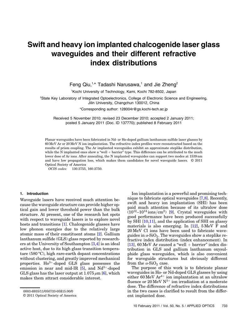
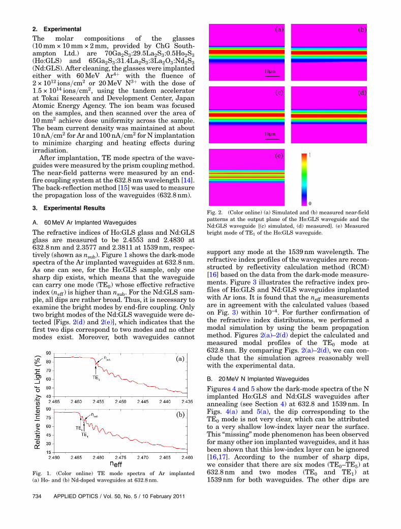
The refractive indices of Ho:GLS glass and Nd:GLSglass are measured to be 2.4553 and 2.4830 at632:8nm and 2.3577 and 2.3811 at 1539nm, respec-tively (shown as nsub). Figure 1 shows the dark-modespectra of the Ar implanted waveguides at 632:8nm.As one can see, for the Ho:GLS sample, only onesharp dip exists, which means that the waveguidecan carry one mode (TE0) whose effective refractiveindex (neff ) is higher than nsub. For the Nd:GLS sam-ple, all dips are rather broad. Thus, it is necessary toexamine the bright modes by end-fire coupling. Onlytwo bright modes of the Nd:GLS waveguide were de-tected [Figs. 2(d) and 2(e)], which indicates that thefirst two dips correspond to two modes and no othermodes exist. Moreover, both waveguides cannot
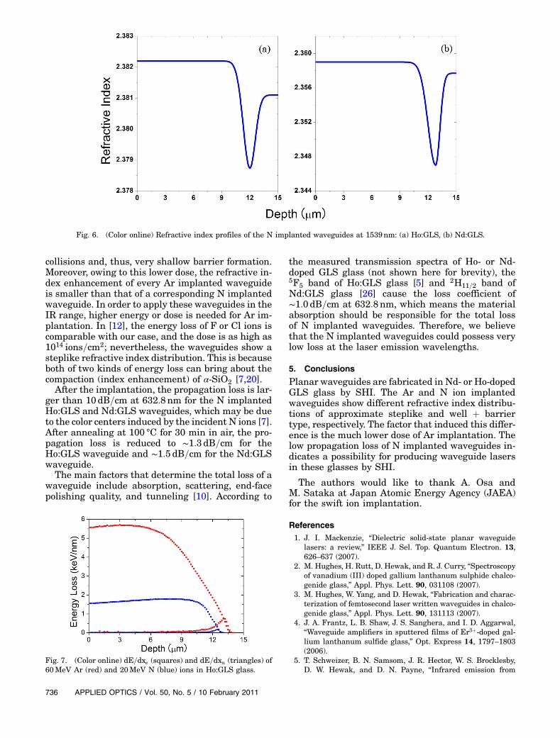
support any mode at the 1539nm wavelength. Therefractive index profiles of the waveguides are recon-structed by reflectivity calculation method (RCM)[16] based on the data from the dark-mode measure-ments. Figure 3 illustrates the refractive index pro-files of Ho:GLS and Nd:GLS waveguides implantedwith Ar ions. It is found that the neff measurementsare in agreement with the calculated values (basedon Fig. 3) within 10−4. For further confirmation ofthe refractive index distributions, we performed amodal simulation by using the beam propagationmethod. Figures 2(a)–2(d) depict the calculated andmeasured modal profiles of the TE0 mode at632:8nm. By comparing Figs. 2(a)–2(d), we can con-clude that the simulation agrees reasonably wellwith the experimental data.
B. 20MeV N Implanted Waveguides
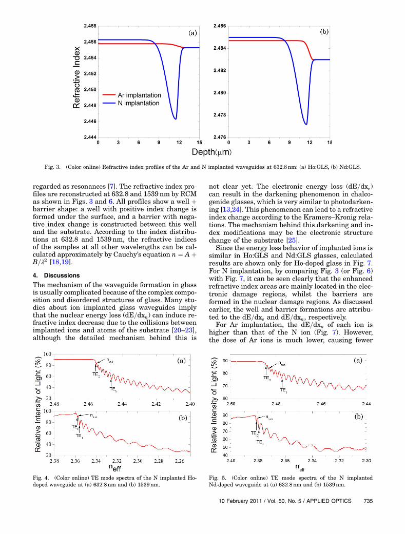
Figures 4 and 5 show the dark-mode spectra of the Nimplanted Ho:GLS and Nd:GLS waveguides afterannealing (see Section 4) at 632.8 and 1539nm. InFigs. 4(a) and 5(a), the dip corresponding to theTE0 mode is not very clear, which can be attributedto a very shallow low-index layer near the surface.This “missing”mode phenomenon has been observedfor many other ion implanted waveguides, and it hasbeen shown that this low-index layer can be ignored[16,17]. According to the number of sharp dips,we consider that there are six modes (TE0–TE5) at632:8nm and two modes (TE0 and TE1) at1539nm for both waveguides. The other dips are
Fig. 1. (Color online) TE mode spectra of Ar implanted(a) Ho- and (b) Nd-doped waveguides at 632:8nm.
Fig. 2. (Color online) (a) Simulated and (b) measured near-fieldpatterns at the output plane of the Ho:GLS waveguide and theNd:GLS waveguide [(c) simulated, (d) measured]. (e) Measuredbright mode of TE1 of the Ho:GLS waveguide.
regarded as resonances [7]. The refractive index pro-files are reconstructed at 632.8 and 1539nm by RCMas shown in Figs. 3 and 6. All profiles show a well þbarrier shape: a well with positive index change isformed under the surface, and a barrier with nega-tive index change is constructed between this welland the substrate. According to the index distribu-tions at 632.8 and 1539nm, the refractive indicesof the samples at all other wavelengths can be cal-culated approximately by Cauchy’s equation n ¼ AþB=λ2 [18,19].
4. Discussions
The mechanism of the waveguide formation in glassis usually complicated because of the complex compo-sition and disordered structures of glass. Many stu-dies about ion implanted glass waveguides implythat the nuclear energy loss (dE=dxn) can induce re-fractive index decrease due to the collisions betweenimplanted ions and atoms of the substrate [20–23],although the detailed mechanism behind this is
not clear yet. The electronic energy loss (dE=dxe)can result in the darkening phenomenon in chalco-genide glasses, which is very similar to photodarken-ing [13,24]. This phenomenon can lead to a refractiveindex change according to the Kramers–Kronig rela-tions. The mechanism behind this darkening and in-dex modifications may be the electronic structurechange of the substrate [25].
Since the energy loss behavior of implanted ions issimilar in Ho:GLS and Nd:GLS glasses, calculatedresults are shown only for Ho-doped glass in Fig. 7.For N implantation, by comparing Fig. 3 (or Fig. 6)with Fig. 7, it can be seen clearly that the enhancedrefractive index areas are mainly located in the elec-tronic damage regions, whilst the barriers areformed in the nuclear damage regions. As discussedearlier, the well and barrier formations are attribu-ted to the dE=dxe and dE=dxn, respectively.
For Ar implantation, the dE=dxn of each ion ishigher than that of the N ion (Fig. 7). However,the dose of Ar ions is much lower, causing fewer
Fig. 4. (Color online) TE mode spectra of the N implanted Ho-doped waveguide at (a) 632:8nm and (b) 1539nm.
Fig. 5. (Color online) TE mode spectra of the N implantedNd-doped waveguide at (a) 632:8nm and (b) 1539nm.
Fig. 3. (Color online) Refractive index profiles of the Ar and N implanted waveguides at 632:8nm: (a) Ho:GLS, (b) Nd:GLS.
collisions and, thus, very shallow barrier formation.Moreover, owing to this lower dose, the refractive in-dex enhancement of every Ar implanted waveguideis smaller than that of a corresponding N implantedwaveguide. In order to apply these waveguides in theIR range, higher energy or dose is needed for Ar im-plantation. In [12], the energy loss of F or Cl ions iscomparable with our case, and the dose is as high as1014 ions=cm2; nevertheless, the waveguides show asteplike refractive index distribution. This is becauseboth of two kinds of energy loss can bring about thecompaction (index enhancement) of α-SiO2 [7,20].
After the implantation, the propagation loss is lar-ger than 10dB=cm at 632:8nm for the N implantedHo:GLS and Nd:GLS waveguides, which may be dueto the color centers induced by the incident N ions [7].After annealing at 100 °C for 30 min in air, the pro-pagation loss is reduced to ∼1:3dB=cm for theHo:GLS waveguide and ∼1:5dB=cm for the Nd:GLSwaveguide.
The main factors that determine the total loss of awaveguide include absorption, scattering, end-facepolishing quality, and tunneling [10]. According to
the measured transmission spectra of Ho- or Nd-doped GLS glass (not shown here for brevity), the5F5 band of Ho:GLS glass [5] and 2H11=2 band ofNd:GLS glass [26] cause the loss coefficient of∼1:0dB=cm at 632:8nm, which means the materialabsorption should be responsible for the total lossof N implanted waveguides. Therefore, we believethat the N implanted waveguides could possess verylow loss at the laser emission wavelengths.
5. Conclusions
Planar waveguides are fabricated in Nd- or Ho-dopedGLS glass by SHI. The Ar and N ion implantedwaveguides show different refractive index distribu-tions of approximate steplike and well þ barriertype, respectively. The factor that induced this differ-ence is the much lower dose of Ar implantation. Thelow propagation loss of N implanted waveguides in-dicates a possibility for producing waveguide lasersin these glasses by SHI.
The authors would like to thank A. Osa andM. Sataka at Japan Atomic Energy Agency (JAEA)for the swift ion implantation.
References1. J. I. Mackenzie, “Dielectric solid-state planar waveguide
lasers: a review,” IEEE J. Sel. Top. Quantum Electron. 13,626–637 (2007).
2. M. Hughes, H. Rutt, D. Hewak, and R. J. Curry, “Spectroscopyof vanadium (III) doped gallium lanthanum sulphide chalco-genide glass,” Appl. Phys. Lett. 90, 031108 (2007).
3. M. Hughes, W. Yang, and D. Hewak, “Fabrication and charac-terization of femtosecond laser written waveguides in chalco-genide glass,” Appl. Phys. Lett. 90, 131113 (2007).
4. J. A. Frantz, L. B. Shaw, J. S. Sanghera, and I. D. Aggarwal,“Waveguide amplifiers in sputtered films of Er3þ-doped gal-lium lanthanum sulfide glass,” Opt. Express 14, 1797–1803(2006).
5. T. Schweizer, B. N. Samsom, J. R. Hector, W. S. Brocklesby,D. W. Hewak, and D. N. Payne, “Infrared emission from
Fig. 6. (Color online) Refractive index profiles of the N implanted waveguides at 1539nm: (a) Ho:GLS, (b) Nd:GLS.
Fig. 7. (Color online) dE=dxe (squares) and dE=dxn (triangles) of60MeV Ar (red) and 20MeV N (blue) ions in Ho:GLS glass.
6. A. K. Mairaj, C. Riziotis, A. M. Chardon, P. G. R. Smith,D. P. Shepherd, and D. W. Hewak, “Development of channelwaveguide lasers in Nd3þ-doped chalcogenide (Ga:La:S) glassthrough photoinduced material modification,” Appl. Phys.Lett. 81, 3708–3710 (2002).
7. P. D. Townsend, P. J. Chandler, and L. Zhang,Optical Effects ofIon Implantation (Cambridge University, 1994).
8. F. Chen, “Construction of two-dimensional waveguides in in-sulating optical materials by means of ion beam implantationfor photonic applications Fabrication methods and researchprogress,” Crit. Rev. Solid State Mater. Sci. 33, 165–182(2008).
9. F. Chen, “Photonic guiding structures in lithium niobate crys-tals produced by energetic ion beams,” J. Appl. Phys. 106,081101 (2009).
10. J. Olivares, G. García, A. García-Navarro, F. Agulló-López,O. Caballero, and A. García-Cabañes, “Generation of high-confinement step-like optical waveguides in LiNbO3 by swiftheavy ion-beam irradiation,” Appl. Phys. Lett. 86, 183501(2005).
11. J. Olivares, A. García-Navarro, G. García, A. Méndez,F. Agulló-López, A. García-Cabañes, M. Carrascosa, andO. Caballero, “Nonlinear optical waveguides generated inlithium niobate by swift-ion irradiation at ultralow fluences,”Opt. Lett. 32, 2587–2589 (2007).
12. J. Manzano, J. Olivares, F. Agulló-Lópeza, M. L. Crespillo,A. Moroño, and E. Hodgson, “Optical waveguides obtainedby swift-ion irradiation on silica (α-SiO2),” Nucl. Instrum.Methods Phys. Res. B 268, 3147–3150 (2010).
13. F. Qiu and T. Narusawa, “Application of swift and heavy ionimplantation to the formation of chalcogenide glass opticalwaveguides,” Opt. Mater. 33, 527–530 (2011).
14. F. Qiu and T. Narusawa, “Proton-implanted planar waveguidein gallium lanthanum sulphide glass,” Jpn. J. Appl. Phys. 49,092503 (2010).
15. R. Ramponi, R. Osellame, and M. Marangoni, “Twostraightforward methods for the measurement of opticallosses in planar waveguides,” Rev. Sci. Instrum. 73,1117–1120 (2002).
16. P. J. Chandler and F. L. Lama, “A new approach to the deter-mination of planar waveguide profiles by means of a non-stationary mode index calculation,” J. Mod. Opt. 33, 127–143(1986).
17. L. Zhang, P. J. Chandler, P. D. Townsend, Z. T. Alwahabi,S. L. Pityana, and A. J. McCaffery, “Frequency doubling inion-implanted KTiOPO4 planar waveguides with 25% conver-sion efficiency,” J. Appl. Phys. 73, 2695–2699 (1993).
18. M. D. Shinn, W. A. Sibley, M. G. Drexhave, and E. N. Brown,“Optical transitions of Er3þ ions in fluorozirconate glass,”Phys. Rev. B 27, 6635–6648 (1983).
19. L. Yang, E. Y. B. Pun, and H. Lin, “Tm3þ-doped ion-exchangedaluminum germanate glass waveguide for S-band amplifica-tion,” Appl. Phys. Lett. 95, 151106 (2009).
20. F. Chen, X. L. Wang, and K. M. Wang, “Development of ion-implanted optical waveguides in optical materials,” Opt.Mater. 29, 1523–1542 (2007).
21. S. L. Li, K. M. Wang, F. Chen, X. L. Wang, G. Fu, Q. M. Lu,L. L. Hu, D. Y. Shen, and H. J. Ma, “Property studies of opticalwaveguide formed by 6:0MeV carbon ion implantation intoNd:silicate glass,” J. Phys. D 38, 2899–2903 (2005).
22. F. Chen, X. L. Wang, X. S. Li, Q. M. Lu, K. M. Wang, B. R. Shi,and D. U. Shen, “Ion-implanted waveguides in Nd3þ-doped si-licate glass and Er3þ=Yb3þ co-doped phosphate glass,” Appl.Surf. Sci. 193, 92–101 (2002).
23. L. Wang, F. Chen, X. L. Wang, K. M. Wang, Y. Jiao, L. L. Wang,X. S. Li, Q. M. Lu, H. J. Ma, and R. Nie, “Low-loss planar andstripe waveguides in Nd3þ-doped silicate glass produced byoxygen-ion implantation,” J. Appl. Phys. 101, 053112 (2007).
24. M. S. Kamboj, G. Kaur, R. Thangaraj, and D. K. Avasthi, “Ef-fect of heavy ion irradiation on the electrical and optical prop-erties of amorphous chalcogenide thin films,” J. Phys. D 35,477–479 (2002).
25. S. Ducharme, J. Hautala, and P. C. Taylor, “Photodarkeningprofiles and kinetics in chalcogenide glasses,” Phys. Rev. B41, 12250–12259 (1990).
26. A. K. Mairaj, A. M. Chardon, D. P. Shepherd, andD. W. Hewak, “Laser performance and spectroscopic analysisof optically written channel waveguides in neodymium-doped gallium lanthanum sulphide glass,” IEEE J. Sel. Top.Quantum Electron. 8, 1381–1388 (2002).