Switch Mode Power Supply Measurements Application Note Agilent’s 3000, 4000, and 6000 X-Series oscilloscopes with the Power Measurements option provide a quick and easy way to analyze the reliability and efficiency of switching power supplies. This application note provides step-by- step instructions on how to perform a broad range of power analysis measurements on your switch mode power supply (SMPS), as well as detailed instructions on how to perform these same measurements when using Agilent’s SMPS Measurements Training Kit as the device under test (DUT). The following power analysis measurements are enabled when an Agilent InfiniiVision 3000, 4000, or 6000 X-Series oscilloscope has been licensed with the Power Measurements option DSOX3PWR/DSOX4PWR/ DSOX6PWR: Introduction Using an Agilent InfiniiVision 3000/4000/6000 X-Series Oscilloscope With the Power Measurements Option Input analysis • Power Quality • Current Harmonics • Inrush Current Switching/modulation analysis • Switching Loss • Slew Rate • Modulation Output analysis • Output Ripple • Turn on/Turn off • Transient Response • Power Supply Rejection Ratio (PSRR) • Efficiency
Transcript
Switch Mode Power Supply Measurements
Application Note
Agilent’s 3000, 4000, and 6000 X-Series oscilloscopes with the Power Measurements option provide a quick and easy way to analyze the reliability and efficiency of switching power supplies. This application note provides step-by-step instructions on how to perform a broad range of power analysis measurements on your switch mode power supply (SMPS), as well as detailed instructions on how to perform these same measurements when using Agilent’s SMPS Measurements Training Kit as the device under test (DUT). The following power analysis measurements are enabled when an Agilent InfiniiVision 3000, 4000, or 6000 X-Series oscilloscope has been licensed with the Power Measurements option DSOX3PWR/DSOX4PWR/DSOX6PWR:
Introduction
Using an Agilent InfiniiVision 3000/4000/6000 X-Series Oscilloscope With the Power Measurements Option
Input analysis • Power Quality • Current Harmonics • Inrush Current
Switching/modulation analysis • Switching Loss • Slew Rate • Modulation
Output analysis • Output Ripple • Turn on/Turn off • Transient Response • Power Supply Rejection Ratio (PSRR) • Efficiency
2
Required equipment • Agilent 3000, 4000, or 6000 X-Series Oscilloscope with the Power Measurements option (DSOX3PWR, DSOX4PWR, or DSOX6PWR) • U1880A Deskew Fixture with USB cable for power • N2790A High-voltage Differential Active Probe, or equivalent • 1147B or N2893A 15A Current Probe, or equivalent • 10:1 Passive Voltage Probe • Your Switch Mode Power Supply (SMPS) or Agilent’s SMPS Measurements Training Kit (Figure 1)
Figure 1: Agilent’s Switch Mode Power Supply Measurements Training Kit.
Table of contents
Introduction…………………….………………..1 Probing tips……………………………………..2 Deskewing the probes…..….……………....4 Power quality analysis….….……………...5 Current harmonics analysis..…………….6 Inrush current analysis .……………...…...7 Switching loss analysis ..…………………8 Slew rate analysis…………….……………..12 Modulation analysis .………………………13 Output ripple analysis ..………………….14 Turn-on/turn-off analysis ..……………..15 Transient response analysis ……………17 PSRR analysis…………………………………19 Efficiency analysis ………………………….21 Related literature…………………………….22
3
If using Agilent’s N2790A high-voltage differential active probe (Figure 2) for your power measurements, this probe can be manually set for either 50:1 attenuation for up to 140 V (DC plus peak AC) measurements, or 500:1 attenuation for up to 1400 V measurements. If you are using Agilent’s SMPS training kit as your DUT, the 50:1 setting is appropriate. But, if you are performing measurements on your own switching power supply that may have higher input and switching voltages, then you may need to use the 500:1 setting.
When you initially connect the N2790A probe to one of the input channels of the Agilent 3000/4000/6000 X-Series oscilloscope, the scope will automatically detect and set its own probe attenuation factor for that channel to 50:1, but if you have the probe attenuation manually set on the probe to 500:1, then you will need to manually enter a 500:1 attenuation factor in the scope’s probe menu for that particular channel.
The 1147B or N2893A current probe (Figure 3) is a 0.1 V/A probe (10:1 attenuation). When this probe is connected to any input channel of an Agilent 3000/4000/6000 X-Series oscilloscope, the scope will automatically detect that a current probe is connected to provide measurements in units of Amps. It will also automatically detect and compensate for the 10:1 probe attenuation. No user settings are required.
When you connect the current probe to a current loop in your device under test, make sure to fully close AND lock the probe clamp. To lock it in place, slide the locking mechanism fully forward until you feel and hear it click in place.
Figure 2: Agilent’s N2790A 100-MHz high-voltage differential active probe.
Figure 3: Agilent’s 1147B 50-MHz, 15A AC/DC current probe.
Probing tips
4
When using the 1147B or N2893A current probe to make current measurements on Agilent’s SMPS training kit, it is very easy to connect to various designed-in PC board current loops. But, if you are making measurements on your own switching power supply, rarely are designed-in current loops available. This means you will probably need to create temporary current loops in your prototype power supply’s circuitry in order to measure current and power. Figure 4 shows an example of a wire-loop in series with the Source terminal on a FET switching device in order to measure drain-to-source current. To measure input AC current, engineers will often just strip back the insulation on the power cord to access the line current wire. Note that although this may be quick and easy, this is NOT an Agilent-recommended technique.
After extended use, a magnetic field can build up in a current probe. When you are making power supply measurements using a current probe, you should occasionally “degauss” (de-magnify) the probe. To do this, simply disconnect the current probe from the device under test, close and lock the current probe clamp, and then press the DEMAG button near the base of the probe where it connects to the scope. Note that you can also calibrate the offset of the probe (and scope) at the same time by rotating the ZERO ADJ thumb-wheel until the baseline current waveform aligns with the ground indicator on the scope’s display.
Figure 4: Creating a special current loop in your power supply to measure current.
Probing tips
5
When using dissimilar type probes, such as a voltage probe and current probe, it is important to perform a probe deskew calibration. This automatic procedure using the recommended U1880A deskew fixture (Figure 5) will null-out the difference in propagation delay between your probes to provide more accurate power measurements. This is especially important for the Switching Loss measurement where just a few nanoseconds can sometimes make a big difference in power and energy loss measurements during the turn-on and turn-off phases of transistor switching.
1. Connect the U1880A’s USB cable between the deskew fixture and the USB port on the back of the oscilloscope. 2. Press the [Default Setup] front panel key. 3. Press the [Analyze] front panel key; then press the Features softkey and select the Power Application. 4. Press the Analysis softkey; then select Power Quality. 5. Press the Signals softkey; then press the Deskew softkey. Note that the automatic deskew calibration is also available within the Current Harmonics and Switching Loss measurement menus. 6. Set the S1 switch on the deskew fixture to the “Small Loop” setting as shown in the on-screen diagram in Figure 6. 7. Connect the N2790A high-voltage differential active probe between the scope’s channel-1 input to J6 (red lead to red test point) and J7 (black lead to black test point) on the U1880A deskew fixture as illustrated in the on-screen diagram. 8. Connect the current probe from the scope’s channel-2 input to the “Small Loop” in the direction indicated on the deskew fixture (current flow towards the top of the board). 9. Press the Auto Deskew softkey on the scope.
When the automatic deskew calibration completes, your scope’s display should look similar to Figure 7. The deskew calibration factor will remain in the channel-2 probe settings menu and is non-volatile. But you can manually change the deskew factor, or perform a “factory default setup” within the scope’s [Save/Recall] menu to reset it back to zero. Performing a standard front panel [Default Setup] will NOT reset the deskew calibration factor.
Deskewing the probes
Figure 5: Agilent’s U1880A deskew fixture.
Figure 6: Deskew Connections diagram.
Figure 7: Deskew display after completing automatic deskew between voltage and current probes.
6
Power quality analysis
Power Quality analysis measures the quality of the input AC line signal that supplies power to your switching power supply while operating. This measurement provides the following input signal quality parameters:
• Real Power (P = VInstantaneous x I Instantaneous Averaged over N cycles) • Apparent Power (S = VRMS x IRMS over N cycles) • Reactive Power (Q = Apparent x SIN(φ)) • Power Factor (PF = Real/Apparent) • Voltage Crest Factor (CF V = VPeak /VRMS) • Current Crest Factor (CF I = IPeak / IRMS) • Phase Angle (φ = ACOS(PF))
1. If using Agilent’s SMPS training kit, set the S2 load switch to the ON position (high-load, maximum current). 2. Press the [Default Setup] front panel key. 3. Press the [Analyze] front panel key; then select the Power Application under the Features softkey. 4. Press the Analysis softkey; then select the Power Quality measurement. 5. Press the Signals softkey. 6 Ensure that Voltage is set to 1 (channel-1), and Current is set to 2 (channel-2). 7. Connect the N2790A high-voltage differential active probe from the scope’s channel-1 input to Line (red lead) and Neutral (back lead) as illustrated in the connections diagram shown in Figure 8. If using Agilent’s SMPS training kit, connect the probe to TP2 (red lead) and TP1 (black lead). 8. Connect the current probe from the scope’s channel-2 input to a wire-loop of the input line signal. If using Agilent’s SMPS training kit, connect the current probe to the J1 loop in the direction indicated. 9. Press the AutoSetup softkey; then press Apply. When AutoSetup is pressed, the scope optimally scales the voltage (yellow trace) and current (green trace) waveforms, turns on the waveform math power waveform (purple trace), and then sets the timebase to display two cycles (default setting) across the screen. Note that if you observe the current waveform (green trace) out of phase relative to the voltage waveform (yellow trace), which will result in negative power waveform pulses (purple trace), then your current probe is probably connected backwards. When Apply is pressed, the 4000 or 6000 X-Series scope will automatically measure all of the power quality parameters as shown in Figure 9. The 3000 X-Series scope will measure just Power Factor, Real Power, Apparent Power, and Reactive Power. To measure the Crest Factor of the voltage and current waveforms, make sure Type is set to Crest; then
Figure 8: Connections diagram for the Power Quality measurement.
Figure 9: Input Power Quality measurements.
press Apply. To measure the phase between the voltage and current waveforms, press the Type softkey, select Phase Angle, and then press the Apply softkey again.
Real PowerP (W)
ReactivePowerQ (VAR)Apparent
PowerS (VA)
Φ
Figure 7: Apparent, Real, and Reactive power
7
Current harmonics analysis
Current harmonics analysis measures the amplitude of frequency components that can be injected back into the AC lines. End-products must often meet specific standards of compliance in order not to disturb other equipment connected to the AC supply grid. This measurement will perform an FFT measurement on the current waveform, compare the results of the amplitudes of odd and even harmonics against a user-selected IEC standard, and also provides color-coded pass/fail indicators for each tested frequency up to the 40th harmonic.
1. If using Agilent’s SMPS training kit, set the S2 load switch to the ON position (high-load, maximum current). 2. Press the [Analyze] front panel key; then select the Power Application under the Features softkey. 3. Press the Analysis softkey; then select the Current Harmonics measurement. 4. Press the Signals softkey. 5. Connect the N2790A voltage probe from the scope’s channel-1 input to Line (red lead) and Neutral (back lead) as illustrated in the connections diagram shown In Figure 10. If using Agilent’s SMPS training kit, connect the probe to TP2 (red lead) and TP1 (black lead). 6. Connect the current probe between the scope’s channel-2 input to a wire-loop of the input line signal. If using Agilent’s SMPS training kit, connect the current probe to the J1 loop in the direction indicated. 7. Ensure that Voltage is set to 1 (channel-1), and Current set to 2 (channel-2). 8. Press AutoSetup. If you use the default settings, the scope will display 20 cycles of the input line voltage (yellow trace) and current (green trace) waveforms on the scope’s display. 9. Press the Settings softkey; then press the Line Freq softkey and set the frequency to either 50 Hz, 60 Hz, or 400 Hz depending upon the line frequency in your part of the world or application. Note that you can also select the appropriate IEC standard to test against in this menu as well. 10. Press the [Back] softkey to return to the previous menu; then press the Apply softkey to begin the Current Harmonics measurement.
When Apply is pressed, the scope performs an FFT waveform math operation (purple trace) on the current waveform with the results shown in a tabular format in the upper half of the scope’s display as shown in Figure 11. The scope measures up to the 40th harmonic and compares against the selected IEC standard. To view the higher harmonics, press the Scroll Harmonics softkey and then rotate the knob.
11. To view the results in a bar chart format, press the Settings softkey, then press the Display softkey and change from the Table setting to the Bar Chart setting as shown in Figure 12.
Figure 10: Connections diagram for the Current Harmonics measurement.
Figure 11: Current Harmonics measurement in a tabular format.
Figure 12: Current Harmonics measurement in a Bar Chart format.
8
Inrush current analysis
Figure 13: Setting “expected” inrush current and peak-to-peak line voltage for a single-shot inrush current measurement.
Inrush Current Analysis measures the peak input current (positive or negative) when power is initially turned on. Since this measurement is based on the acquisition of a single-shot event, there is not an AutoSetup selection for this measurement (AutoSetup requires a repetitive input signal). For this reason, you must enter the “expected” peak current surge, as well as the steady-state peak-to-peak line voltage so that the scope can establish initial vertical scaling. The scope then provides step-by-step instructions on how to perform this single-shot measurement. 1. If using Agilent’s Power Measurements training kit, set the S2 load switch to the ON position (high-load, maximum current). 2. Press the [Analyze] front panel key; then select the Power Application under the Features softkey. 3. Press the Analysis softkey; then select the Inrush Current measurement. 4. Press the Signals softkey; then connect the N2790A voltage probe between the scope’s channel-1 input to Line (red lead) and Neutral (back lead) as illustrated in the connections diagram shown in Figure 13. If using Agilent’s SMPS training kit, connect to TP2 (red lead) and TP1 (black lead) on the demo board. 5. Connect the current probe between the scope’s channel-2 input to a wire-loop of the input Line signal. If using Agilent’s training kit, connect the current probe to the J1 loop in the direction indicated. 6. Ensure that Voltage is set to 1 (channel-1), and Current is set to 2 (channel-2). 7. Set Max Vin and the approximate Expected surge current for your device under test. If using Agilent’s SMPS training kit, then the default settings should be appropriate for this measurement.
Note that the default Expected surge current and Max Vin settings have been optimized (default setup) for Agilent’s SMPS training kit. Although the steady-state peak current of the demo board is approximately 1 A (with the S2 load switch set ON), the peak inrush current is much higher and can sometimes exceed ± 30 A. Determining the “expected” peak current of your device under test will be an iterative/trial & error process. The value that you enter for Expected should be higher than the actual peak current that will be captured and measured. 8. After accepting or changing the settings in the Signals menu, press the [Back] front panel key (left side of scope) to return to the previous menu. 9. Press the Apply softkey; then follow the step- by-step on-screen instructions, which are repeated below. 10. Turn OFF power; then press Next.
Figure 14: Inrush current measurement.
11. Turn ON power; then press Next. 12. Repeat several times in order to obtain the worst-case peak inrush current as shown in Figure 14.
If the Peak Current measurement indicates either “>” or “<”, this is an indication that the current waveform is “clipped” and that you should then increase the Expected current setting in the Signals menu for a more accurate measurement. The absolute peak inrush current will typically occur if the power switch is turned on at the same instance in time that the input line voltage is either at its absolute positive or negative peak value. This means that you should repeat this measurement several times in order to measure the worst-case inrush current.
Peak surge
9
Switching loss analysis
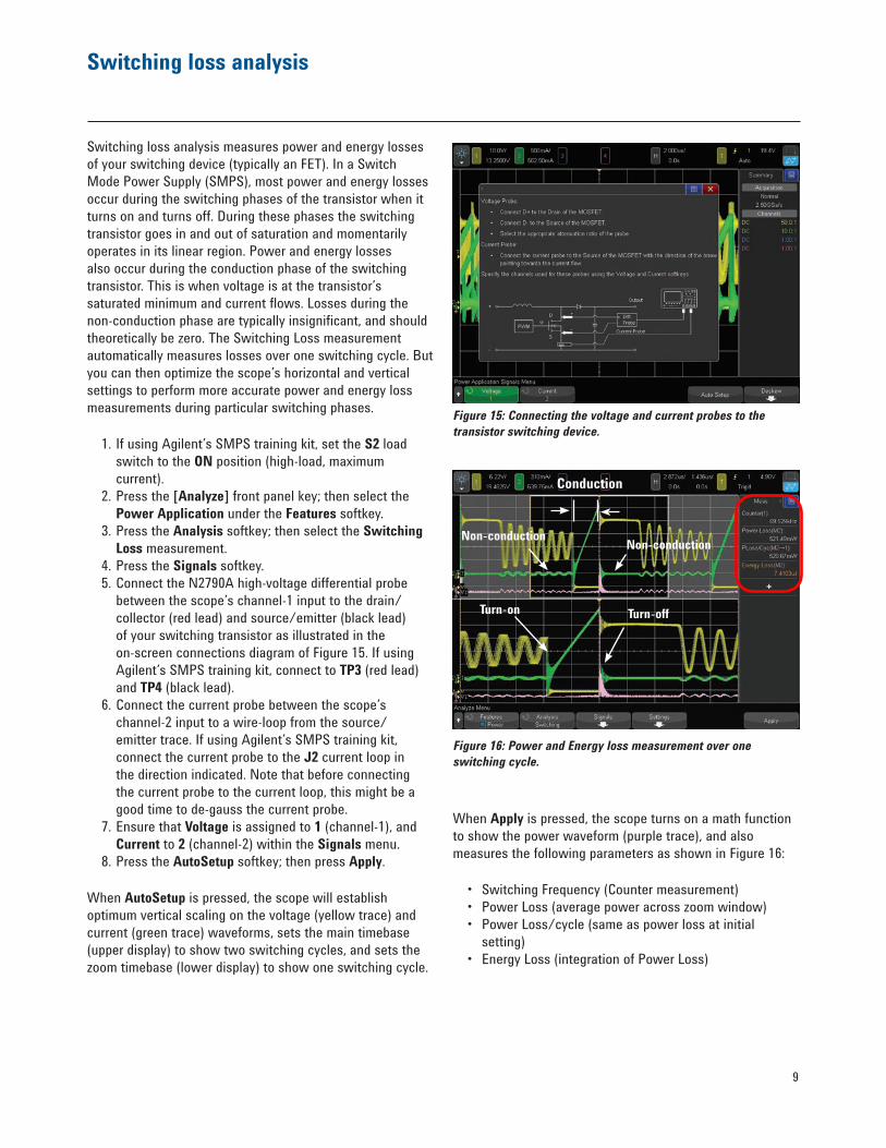
Switching loss analysis measures power and energy losses of your switching device (typically an FET). In a Switch Mode Power Supply (SMPS), most power and energy losses occur during the switching phases of the transistor when it turns on and turns off. During these phases the switching transistor goes in and out of saturation and momentarily operates in its linear region. Power and energy losses also occur during the conduction phase of the switching transistor. This is when voltage is at the transistor’s saturated minimum and current flows. Losses during the non-conduction phase are typically insignificant, and should theoretically be zero. The Switching Loss measurement automatically measures losses over one switching cycle. But you can then optimize the scope’s horizontal and vertical settings to perform more accurate power and energy loss measurements during particular switching phases.
1. If using Agilent’s SMPS training kit, set the S2 load switch to the ON position (high-load, maximum current). 2. Press the [Analyze] front panel key; then select the Power Application under the Features softkey. 3. Press the Analysis softkey; then select the Switching Loss measurement. 4. Press the Signals softkey. 5. Connect the N2790A high-voltage differential probe between the scope’s channel-1 input to the drain/ collector (red lead) and source/emitter (black lead) of your switching transistor as illustrated in the on-screen connections diagram of Figure 15. If using Agilent’s SMPS training kit, connect to TP3 (red lead) and TP4 (black lead). 6. Connect the current probe between the scope’s channel-2 input to a wire-loop from the source/ emitter trace. If using Agilent’s SMPS training kit, connect the current probe to the J2 current loop in the direction indicated. Note that before connecting the current probe to the current loop, this might be a good time to de-gauss the current probe. 7. Ensure that Voltage is assigned to 1 (channel-1), and Current to 2 (channel-2) within the Signals menu. 8. Press the AutoSetup softkey; then press Apply.
When AutoSetup is pressed, the scope will establish optimum vertical scaling on the voltage (yellow trace) and current (green trace) waveforms, sets the main timebase (upper display) to show two switching cycles, and sets the zoom timebase (lower display) to show one switching cycle.
Figure 15: Connecting the voltage and current probes to the transistor switching device.
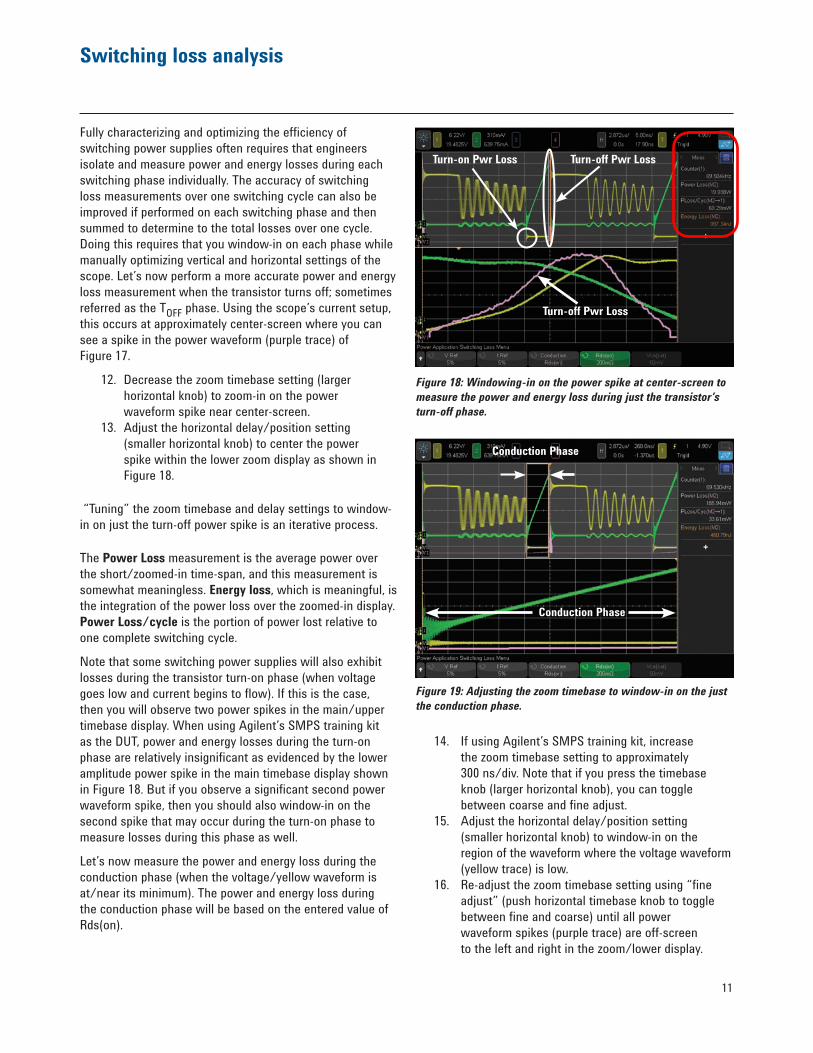
Figure 16: Power and Energy loss measurement over one switching cycle.
When Apply is pressed, the scope turns on a math function to show the power waveform (purple trace), and also measures the following parameters as shown in Figure 16:
• Switching Frequency (Counter measurement) • Power Loss (average power across zoom window) • Power Loss/cycle (same as power loss at initial setting) • Energy Loss (integration of Power Loss)
Conduction
Non-conduction Non-conduction
Turn-on Turn-off
10
Switching loss analysis
Figure 17: Measuring power and energy loss over one switching cycle based on an entered value of Rds(on).
Oscilloscopes don’t typically have sufficient dynamic range and resolution to perform accurate power and energy loss measurements during the conduction and non-conduction phases based on the voltage and current waveforms (Power = Voltage x Current). When amplitudes of the voltage and current waveform are near zero, a few tenths of a division of oscilloscope and/or probe offset error (even if they are within specification) can contribute to significant measurement error. Power and energy loss measurements can be performed more accurately if power is computed during the conduction phase using a entered and specified value of Rds(on) or Vce(sat). The scope will then compute and plot the power waveform based on the measured current waveform during just the conduction phase using the entered constant to compute power (Pwr = I2Rds(on) or IxVce(sat)). Let’s now setup the scope to perform a power and energy loss measurement over one switching cycle based on Rds(on). 9. Press the Settings softkey. 10. Press the Conduction Waveform softkey; then change from the Voltage Waveform setting to the Rds(on) setting. 11. Press the Rds(on) softkey; then enter an appropriate value of Rds(on) for your DUT. If using Agilent’s SMPS training kit, enter 200 mΩ.
Your scope’s display should now look similar to Figure 17, and the power and energy loss measurements shown on the right-hand side of the display should be more accurate — assuming that the entered value of Rds(on) is correct for the device under test. Compare the results of this power and energy loss measurement over one switching cycle based on an entered value of Rds(on) to the measurement shown in Figure 16, which was based purely on the digitized values of the voltage and current waveforms. When you select to make power and energy loss measurements based on Rds(on) or Vce(sat), the scope uses the V Ref and I Ref settings (also set in the Settings menu) to determine to the appropriate method for computing the power waveform for each switching phase. When the voltage waveform (yellow trace) is above the V Ref setting (default = 5%), the scope computes the power waveform as the product of the voltage and current waveforms (V x I). This typically only occurs during the transistor turn-on and turn-off phases. Note that you may
observe a large power spike near center-screen (turn-off), and possibly a shorter power spike (turn-on) coincident with the voltage waveform when it drops to near zero volts. It is during these relatively short phases of the waveform that the scope computes the power based on the product of the instantaneous voltage and current waveforms.
When the voltage waveform is below the V Ref setting, the scope will compute the power waveform as either I2Rds(on) or I x Vce(sat). This provides for a more accurate measure of losses during the conduction phase. We will zoom-in on this segment of the waveform next.
If the current waveform is below the I Ref setting (default = 5%), then the scope will compute the power waveform as V x 0 Amps, which will always be zero Watts. The scope uses this calculation method during the non-conduction phase of the switching waveforms when current drops to zero (theoretically).
11
Switching loss analysis
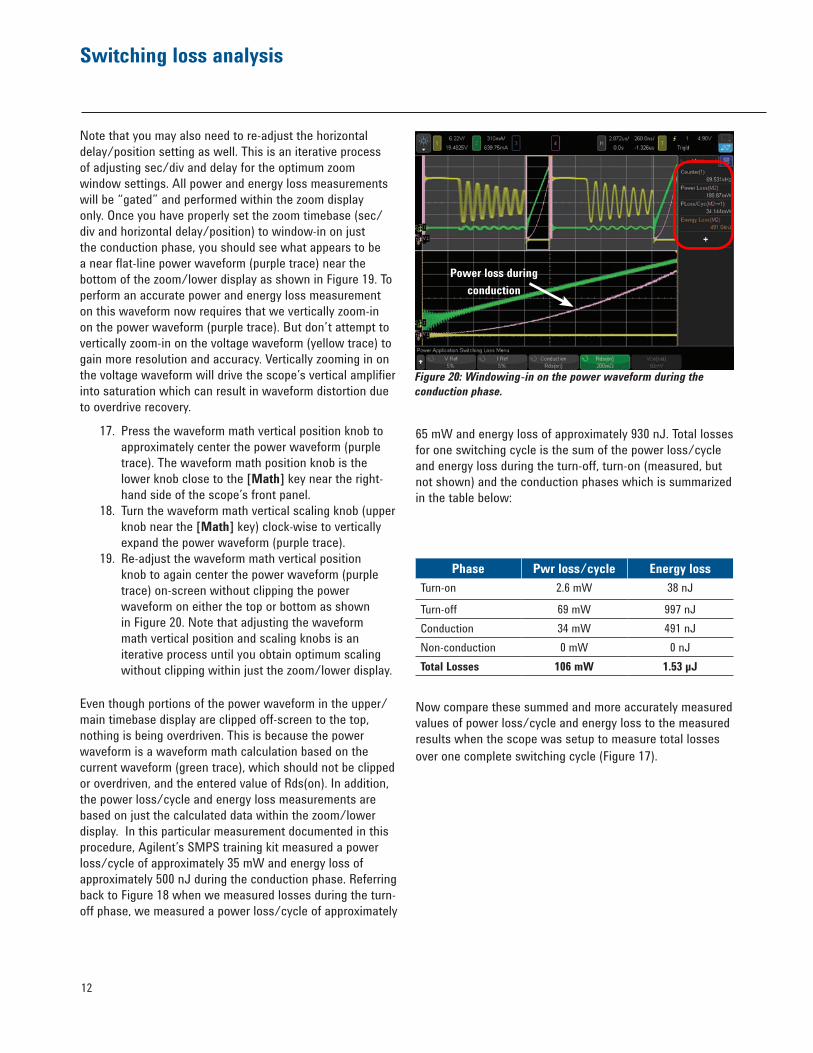
Fully characterizing and optimizing the efficiency of switching power supplies often requires that engineers isolate and measure power and energy losses during each switching phase individually. The accuracy of switching loss measurements over one switching cycle can also be improved if performed on each switching phase and then summed to determine to the total losses over one cycle. Doing this requires that you window-in on each phase while manually optimizing vertical and horizontal settings of the scope. Let’s now perform a more accurate power and energy loss measurement when the transistor turns off; sometimes referred as the TOFF phase. Using the scope’s current setup, this occurs at approximately center-screen where you can see a spike in the power waveform (purple trace) of Figure 17.
12. Decrease the zoom timebase setting (larger horizontal knob) to zoom-in on the power waveform spike near center-screen. 13. Adjust the horizontal delay/position setting (smaller horizontal knob) to center the power spike within the lower zoom display as shown in Figure 18.
“Tuning” the zoom timebase and delay settings to window-in on just the turn-off power spike is an iterative process.
The Power Loss measurement is the average power over the short/zoomed-in time-span, and this measurement is somewhat meaningless. Energy loss, which is meaningful, is the integration of the power loss over the zoomed-in display. Power Loss/cycle is the portion of power lost relative to one complete switching cycle.
Note that some switching power supplies will also exhibit losses during the transistor turn-on phase (when voltage goes low and current begins to flow). If this is the case, then you will observe two power spikes in the main/upper timebase display. When using Agilent’s SMPS training kit as the DUT, power and energy losses during the turn-on phase are relatively insignificant as evidenced by the lower amplitude power spike in the main timebase display shown in Figure 18. But if you observe a significant second power waveform spike, then you should also window-in on the second spike that may occur during the turn-on phase to measure losses during this phase as well.
Let’s now measure the power and energy loss during the conduction phase (when the voltage/yellow waveform is at/near its minimum). The power and energy loss during the conduction phase will be based on the entered value of Rds(on).
Figure 18: Windowing-in on the power spike at center-screen to measure the power and energy loss during just the transistor’s turn-off phase.
Figure 19: Adjusting the zoom timebase to window-in on the just the conduction phase.
14. If using Agilent’s SMPS training kit, increase the zoom timebase setting to approximately 300 ns/div. Note that if you press the timebase knob (larger horizontal knob), you can toggle between coarse and fine adjust. 15. Adjust the horizontal delay/position setting (smaller horizontal knob) to window-in on the region of the waveform where the voltage waveform (yellow trace) is low. 16. Re-adjust the zoom timebase setting using “fine adjust” (push horizontal timebase knob to toggle between fine and coarse) until all power waveform spikes (purple trace) are off-screen to the left and right in the zoom/lower display.
Turn-on Pwr Loss Turn-off Pwr Loss
Turn-off Pwr Loss
Conduction Phase
Conduction Phase
12
Switching loss analysis
Note that you may also need to re-adjust the horizontal delay/position setting as well. This is an iterative process of adjusting sec/div and delay for the optimum zoom window settings. All power and energy loss measurements will be “gated” and performed within the zoom display only. Once you have properly set the zoom timebase (sec/div and horizontal delay/position) to window-in on just the conduction phase, you should see what appears to be a near flat-line power waveform (purple trace) near the bottom of the zoom/lower display as shown in Figure 19. To perform an accurate power and energy loss measurement on this waveform now requires that we vertically zoom-in on the power waveform (purple trace). But don’t attempt to vertically zoom-in on the voltage waveform (yellow trace) to gain more resolution and accuracy. Vertically zooming in on the voltage waveform will drive the scope’s vertical amplifier into saturation which can result in waveform distortion due to overdrive recovery.
17. Press the waveform math vertical position knob to approximately center the power waveform (purple trace). The waveform math position knob is the lower knob close to the [Math] key near the right- hand side of the scope’s front panel. 18. Turn the waveform math vertical scaling knob (upper knob near the [Math] key) clock-wise to vertically expand the power waveform (purple trace). 19. Re-adjust the waveform math vertical position knob to again center the power waveform (purple trace) on-screen without clipping the power waveform on either the top or bottom as shown in Figure 20. Note that adjusting the waveform math vertical position and scaling knobs is an iterative process until you obtain optimum scaling without clipping within just the zoom/lower display.
Even though portions of the power waveform in the upper/main timebase display are clipped off-screen to the top, nothing is being overdriven. This is because the power waveform is a waveform math calculation based on the current waveform (green trace), which should not be clipped or overdriven, and the entered value of Rds(on). In addition, the power loss/cycle and energy loss measurements are based on just the calculated data within the zoom/lower display. In this particular measurement documented in this procedure, Agilent’s SMPS training kit measured a power loss/cycle of approximately 35 mW and energy loss of approximately 500 nJ during the conduction phase. Referring back to Figure 18 when we measured losses during the turn-off phase, we measured a power loss/cycle of approximately
Figure 20: Windowing-in on the power waveform during the conduction phase.
65 mW and energy loss of approximately 930 nJ. Total losses for one switching cycle is the sum of the power loss/cycle and energy loss during the turn-off, turn-on (measured, but not shown) and the conduction phases which is summarized in the table below:
Phase Pwr loss/cycle Energy lossTurn-on 2.6 mW 38 nJ
Now compare these summed and more accurately measured values of power loss/cycle and energy loss to the measured results when the scope was setup to measure total losses over one complete switching cycle (Figure 17).
Power loss during conduction
13
Slew rate analysis
Slew rate analysis measures the rate of change of the voltage and/or current waveform when the switching transistor of your power supply switches on and off.
1. If using Agilent’s SMPS training kit, set the S2 load switch to the ON position (high-load, maximum current). 2. Press the [Analyze] front panel key; then select the Power Application under the Features softkey. 3. Press the Analysis softkey; then select the Slew Rate measurement. 4. Press the Signals softkey; then connect the N2790A voltage probe between channel-1 of the scope to the drain/collector (red lead) and source/emitter (black lead) of your switching transistor as illustrated in the on-screen connections diagram of Figure 21. If using Agilent’s SMPS training kit, connect to TP3 (red lead) and TP4 (black lead). 5. Connect the current probe to a wire-loop of the source/emitter trace. If using Agilent’s SMPS training kit, connect the current probe to the J2 current loop in the direction indicated. 6. Ensure that Voltage is set to 1 (channel-1), and Current is set to 2 (channel-2). 7. Press the AutoSetup softkey; then press Apply.
Your scope’s display should now look similar to Figure 22. AutoSetup will optimally scale the voltage and current waveforms, sets the main timebase (upper display) to show one switching cycle across screen, and sets the zoom timebase (lower display) windowed-in on the turn-off phase of the switching voltage and current waveforms.
When Apply is pressed, the scope turns on the differentiate (dv/dt) math function (purple trace) based on the voltage waveform in order to dynamically plot the slew rate of the voltage waveform. Apply also turns on the Max and Min measurements in order to automatically measure the maximum and minimum slew rates of this waveform.
To measure the maximum and minimum slew rates of the current waveform, press the Source softkey and change the source setting from Voltage to Current.
To measure the slew rates of the voltage and current waveform during the transistor turn-on phase, adjust the horizontal delay/position knob until the zoom timebase is windowed-in on the turn-on phase (when voltage drops to near zero) as shown in Figure 23. Note that for a more stable display of the turn-on phase, you may want to leave the delay setting at zero, but then change the trigger edge from rising to falling. This will establish a more stable trigger during the turn-on phase with the zoom display centered on-screen.
Figure 22: Slew rate measurement of the voltage waveform during the transistor’s turn-off phase.
Figure 23: Slew rate measurement of the current waveform during the transistor turn-on phase.
dv/dt
14
Modulation analysis
Modulation analysis is typically used to characterize the pulse-width modulation (PWM) feedback from the DC output to the switching transistor’s gate terminal for dynamic voltage regulation. Unfortunately, this measurement cannot be demonstrated using Agilent’s SMPS training kit since the FET’s Gate terminal is not accessible for probing.
1. Press the [Analyze] front panel key; then select the Power Application under the Features softkey. 2. Press the Analysis softkey; then select the Modulation measurement. 3. Press the Signals softkey. 4. Connect the N2790A voltage probe between channel-1 of the scope to the gate/base (red lead) and source/ emitter (black lead) of your switching transistor as illustrated in the on-screen connections diagram of Figure 24. Note that although the connection diagrams also shows a current probe connected to the drain, this probe connection is not necessary for this measurement. 5. Ensure that Voltage is set to 1 (channel-1). 6. Press the AutoSetup softkey; then press Apply.
When AutoSetup is pressed the scope optimally scales the voltage waveform (gate-to-source signal) and sets the timebase based on the user-defined Duration setting.
When Apply is pressed, the scope turns on the Measurement Trend waveform math function (purple trace) based on sequential Duty Cycle measurements of the Gate-to-Source signal (yellow trace) across the scope’s display as shown in Figure 25. This is basically a plot of duty cycle on the vertical axis and time on the horizontal axis.
In this example, we have rescaled the timebase to 200 µs/div (2 ms duration) in order to optimally observe duty cycle modulation of the gate signal. The duty cycle of this switching device’s gate signal appears to be modulating at a 1 kHz rate with a maximum measured duty cycle of approximately 15% and minimum measured duty cycle of approximately 13%.
The Modulation measurement can also be very useful for characterizing turn-on characteristics of your switching power supply. Figure 26 shows an example of a single-shot measurement of the frequency of the switching transistor’s Gate signal when power is initially applied. In this case we have changed the measurement Type from Duty Cycle to Frequency, and then manually set up the scope to perform a single-shot acquisition. In this example we can observe the amplitude of the gate-to-source signal (yellow trace) ramp up to its steady-state condition in approximately 1.8 ms. And the Measurement Trend waveform (purple trace), which is based on sequential frequency measurements of the Gate signal across the display, shows that the transistor quickly ramps up to a steady-state switching frequency of 69 kHz in 600 µs.
Figure 25: Modulation measurement of Duty Cycle on the switching transistor’s Gate input.
Figure 26: Modulation measurement of Frequency on the switching transistor’s Gate input during power-up.
Measurement trend waveform of duty cycle
Measurement Trend waveform of Frequency
15
Output ripple analysis
Output ripple analysis measures the peak-to-peak extremes of the output DC signal of your power supply. It also measures AC-RMS of the output DC signal. The AC-RMS measurement is the same as Standard Deviation (σ), which is a commonly-used measurement to characterize random noise. Output Ripple is typically dominated by switching noise, but can also include other random noise and signal coupling from various sources in your system. This measurement basically measures the quality of the power supply’s voltage regulation and filtering to reject switching noise, as well as other noise/interference sources.
1. If using Agilent’s SMPS training kit, set the S2 load switch to the ON position (high-load, maximum current). 2. Press the [Analyze] front panel key; then select the Power Application under the Features softkey. 3. Press the Analysis softkey; then select the Output Ripple measurement. 4. Press the Signals softkey 5. Connect a standard 10:1 passive voltage probe between the scope’s channel-3 input to the DC output signal and ground as illustrated in the on-screen connections diagram shown in Figure 27. If using Agilent’s SMPS training kit, connect the 10:1 passive probe from channel-3 to TP5 (probe tip grabber) and TP6 (ground). 6. Press the Voltage softkey; then change setting to 3 (measured source will be channel-3). 7. Press the AutoSetup softkey; then press Apply.
Your scope’s display should now look similar to Figure 28. When AutoSetup is pressed the scope AC couples the input signal on the selected channel to eliminate the DC component, and then optimally scales the selected input channel’s vertical setting to display just the output ripple of the DC output signal.
When Apply is pressed, the scope measures the output ripple of the DC output signal in terms of peak-to-peak voltage, as well as AC-RMS (σ).
Note that for a well-regulated power supply that generates a very low level of output ripple, a 1:1 passive probe such as Agilent’s N2870A or 100070D, may be required for this measurement.
Figure 28: Output Ripple measurement on the DC output signal.
16
Turn on/turn off analysis
Turn-on analysis measures the time from when power is initially switched on until the dc output reaches 90% of its expected steady-state level. Turn-off analysis measures the time from when power is switched off until the DC output decays to 10% of the steady-state on level.
1. If using Agilent’s SMPS training kit, set the S2 load switch to the ON position (high-load, maximum current). 2. Press the [Analyze] front panel key; then select the Power Application under the Features softkey. 3. Press the Analysis softkey; then select the Turn On/ Turn Off measurement. 4. Press the Signals softkey. 5. Connect the N2790A differential active probe between the scope’s channel-1 input to Line (red lead) and Neutral (black lead) as illustrated in the on-screen connections diagram shown in Figure 29. If using Agilent’s power training kit, connect to TP2 (red lead) and TP1 (black lead). 6. Connect a standard 10:1 passive voltage probe between the scope’s channel-3 input to the DC output of your DUT. If using Agilent’s SMPS training kit, connect to TP5 (probe tip grabber) and TP6 (ground). 7. Press the Input V softkey; then set to 1 (channel-1). 8. Press the Output V softkey; then set to 3 (channel-3).
Note that the default settings for Duration, Max Vin, and Steady Vout have been optimized for Agilent’s SMPS training kit. If testing a different power supply, then enter the appropriate values for Max Vin (peak-to-peak) and Steady Vout. Also, you may want to begin your test with the default Duration setting of 500 ms, which will determine the scope’s timebase setting for this measurement.
9. Press the [Back] front panel key to return to the previous menu. 10. Press the Apply softkey to begin the test; then follow on-screen instructions, which are repeated below. 11. Turn OFF power; then press Next. 12. Turn ON power; then press Next.
If the turn-on time of your device under test is less than 400 ms, then your scope’s display should look similar to Figure 30. If the initial Duration setting is too low, then the measurement cannot be performed. If this is the case, then set the Duration time to a higher value as indicated by the on-screen message; then try again. Alternatively, to improve the timing resolution of this measurement you may want to set the Duration time to a lower value. After determining the best Duration time for this measurement, repeat the test several times to determine best- and worst-case turn-on time. Figure 31 shows this same test with the Duration time set to 50 ms.
Figure 29: Turn-on/Turn-off connections diagram in the Signals menu.
Figure 30: Turn-on test using a default Duration time setting of 500 ms.
Figure 31: Turn-on time test using a Duration time setting of 50 ms to improve measurement resolution and accuracy.
DC Output
AC Input
17
Turn on/turn off analysis
Let’s now perform a turn-off time measurement.
13. Continuing from the previous Turn On time measurement, press the Test softkey; then change from Turn On to Turn Off. 14. Press the Signals softkey; then note the default settings of Duration, Max Vin, and Steady Vout. These setting have been optimized for Agilent’s SMPS training kit used in this demo procedure. If testing a different power supply, Max Vin and Steady Vout should already be set to the correct values based on the previous Turn On test. But the default Duration time setting of 1.00 second may not be a valid setting for your power supply. 15. Press the [Back] front panel key to return to the previous menu; then press the Apply softkey and follow the step-by-step on-screen instructions, which are repeated below. 16. Turn ON power; then press Next. 17. Turn OFF power; then press Next.
Your scope’s display should now look similar to Figure 32. Repeat this measurement several times to determine the best- and worst-case turn-off times. Note that you may need to adjust the Duration time setting for this test.
If using Agilent’s SMPS training kit for this measurement, try setting the S2 switch to the OFF position (low-load, minimum current) and then repeat the Turn Off time measurement. You will probably need to increase the Duration time to 2.0 seconds with the S2 load switch in the OFF position. With a decreased output load, the output will decay more slowly when power is turned off.
Figure 32: Turn-off time test.
DC Output
AC Input
18
Transient response analysis
Figure 33: Transient Response connections diagram in the Signals menu.
Transient response analysis measures the time for the output DC voltage to settle within a user-set percentage of the expected output level after a sudden change in output load (increase or decrease in output current). Before setting up this measurement, you must first determine what the approximate output current levels are for various load conditions.
1. If using Agilent’s SMPS training kit, set the S2 load switch to the OFF position (low-load, minimum current). 2. Press the [Analyze] front panel key; then select the Power Application under the Features softkey. 3. Press the Analysis softkey; then select the Transient Response measurement. 4. Press the Signals softkey. 5. Connect the current probe between the scope’s channel-2 input to the output current signal on your device under test as illustrated in the on-screen connections diagram shown in Figure 33. If using Agilent’s SMPS training kit, connect to the J3 current loop in the direction indicated on the demo board. Note that the current-direction arrow on the current probe should be facing down towards your bench. 6. Connect a standard 10:1 passive voltage probe between the scope’s channel-3 input to the output DC voltage signal. If using Agilent’s power demo board, connect to TP5 (probe tip grabber) and TP6 (ground). 7. Press the Voltage softkey; then select 3 (channel-3). 8. Press the Current softkey; then select 2 (channel-2). 9. Set the Steady Vout for your DUT. If using Agilent’s SMPS training kit, the default level of 12.0 V is appropriate. 10. Press the [Back] front panel to return to the previous menu. 11. Press the Settings softkey; then set Initial I to the approximate low-load output current level (assuming that the S2 load switch is in the OFF position (low- load/low current). Also set the New I to the approximate high-load output current level. If using Agilent’s SMPS training kit, you can use the default settings of 60 mA and 215 mA respectively. 12. Press the [Back] front panel key to return to the previous menu. 13. Press the Apply softkey; then follow the on-screen step-by-step instructions, which are repeated below. 14. Increase the output load (higher current). If using Agilent’s SMPS training kit, move the S2 load switch to the ON position (away from the J3 current loop). 15. Press Next.
Figure 34: Transient Response settling time measurement when output load increases (output current suddenly increases).
Your scope’s display should now look similar to Figure 34. When output current measured by the channel-2 current probe (green trace) suddenly increases, output voltage (blue trace) momentarily drops and then settles back to within 10% of the expected output voltage level in approximately 12 ns.
V-out transient
I-out increase
19
Transient response analysis
Let’s now perform this Transient Response settling time measurement for when the output load decreases (lower output current).
16. If using Agilent’s SMPS training kit, make sure that the S2 load switch is now in the ON position (away from the J3 current loop). This will put the training kit into an initial high-load (high output current) condition. 17. Press the Settings softkey; if using Agilent’s SMPS training kit, then set Initial I to approximately 200 mA, and New I to approximately 60 mA. If making transient response measurements on your own power supply, then set to appropriate values. 18. Press the [Back] front panel key to return to the previous menu. 19. Press the Apply softkey; then follow the on-screen step-by-step instructions, which are repeated below. 20. Decrease the output load (lower current). If using Agilent’s SMPS training kit, move the S2 load switch to the OFF position (towards the J3 current loop). 21. Press Next.
Your scope’s display should now look similar to Figure 35. When output current (green trace) suddenly drops, output voltage (blue trace) momentarily increases and then settles to within 10% of the expected output voltage level in approximately 21 ns.
Note the Transient Response settling time measurement for both increasing and decreasing load conditions should be repeated several times in order to characterize best- and worst-case settling times.
Figure 35: Transient Response settling time measurement when output load decreases (output current suddenly decreases).
V-out transient
I-out decrease
20
PSRR analysis
Figure 36: PSRR connections diagram in the Signals menu.
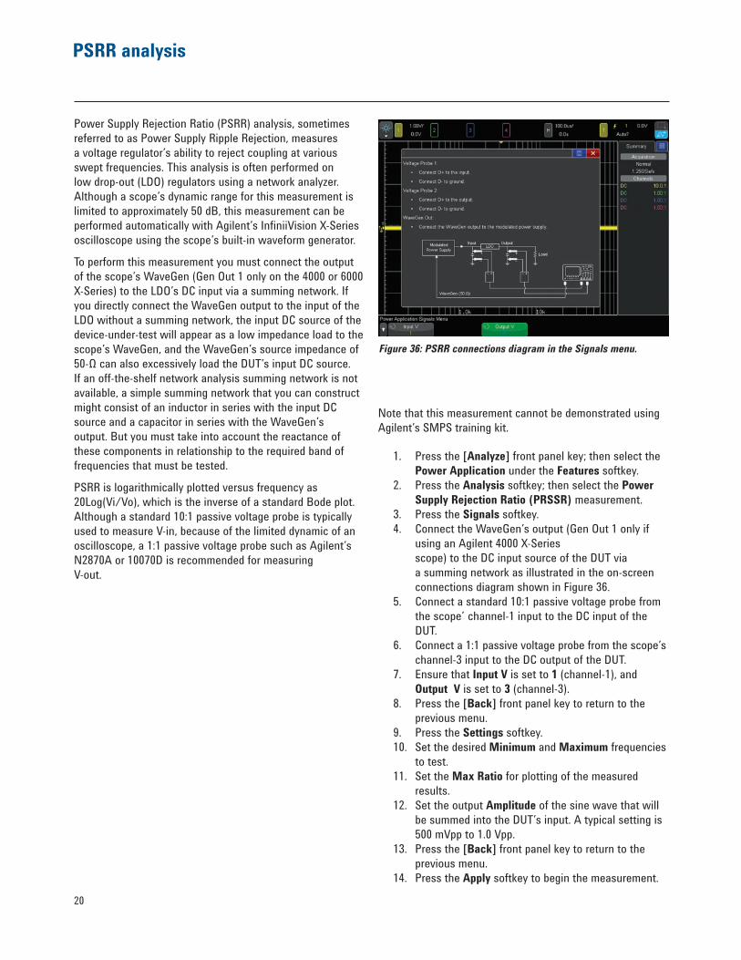
Power Supply Rejection Ratio (PSRR) analysis, sometimes referred to as Power Supply Ripple Rejection, measures a voltage regulator’s ability to reject coupling at various swept frequencies. This analysis is often performed on low drop-out (LDO) regulators using a network analyzer. Although a scope’s dynamic range for this measurement is limited to approximately 50 dB, this measurement can be performed automatically with Agilent’s InfiniiVision X-Series oscilloscope using the scope’s built-in waveform generator.
To perform this measurement you must connect the output of the scope’s WaveGen (Gen Out 1 only on the 4000 or 6000 X-Series) to the LDO’s DC input via a summing network. If you directly connect the WaveGen output to the input of the LDO without a summing network, the input DC source of the device-under-test will appear as a low impedance load to the scope’s WaveGen, and the WaveGen’s source impedance of 50-Ω can also excessively load the DUT’s input DC source. If an off-the-shelf network analysis summing network is not available, a simple summing network that you can construct might consist of an inductor in series with the input DC source and a capacitor in series with the WaveGen’s output. But you must take into account the reactance of these components in relationship to the required band of frequencies that must be tested.
PSRR is logarithmically plotted versus frequency as 20Log(Vi/Vo), which is the inverse of a standard Bode plot. Although a standard 10:1 passive voltage probe is typically used to measure V-in, because of the limited dynamic of an oscilloscope, a 1:1 passive voltage probe such as Agilent’s N2870A or 10070D is recommended for measuring V-out.
1. Press the [Analyze] front panel key; then select the Power Application under the Features softkey. 2. Press the Analysis softkey; then select the Power Supply Rejection Ratio (PRSSR) measurement. 3. Press the Signals softkey. 4. Connect the WaveGen’s output (Gen Out 1 only if using an Agilent 4000 X-Series scope) to the DC input source of the DUT via a summing network as illustrated in the on-screen connections diagram shown in Figure 36. 5. Connect a standard 10:1 passive voltage probe from the scope’ channel-1 input to the DC input of the DUT. 6. Connect a 1:1 passive voltage probe from the scope’s channel-3 input to the DC output of the DUT. 7. Ensure that Input V is set to 1 (channel-1), and Output V is set to 3 (channel-3). 8. Press the [Back] front panel key to return to the previous menu. 9. Press the Settings softkey. 10. Set the desired Minimum and Maximum frequencies to test. 11. Set the Max Ratio for plotting of the measured results. 12. Set the output Amplitude of the sine wave that will be summed into the DUT’s input. A typical setting is 500 mVpp to 1.0 Vpp. 13. Press the [Back] front panel key to return to the previous menu. 14. Press the Apply softkey to begin the measurement.
Note that this measurement cannot be demonstrated using Agilent’s SMPS training kit.
21
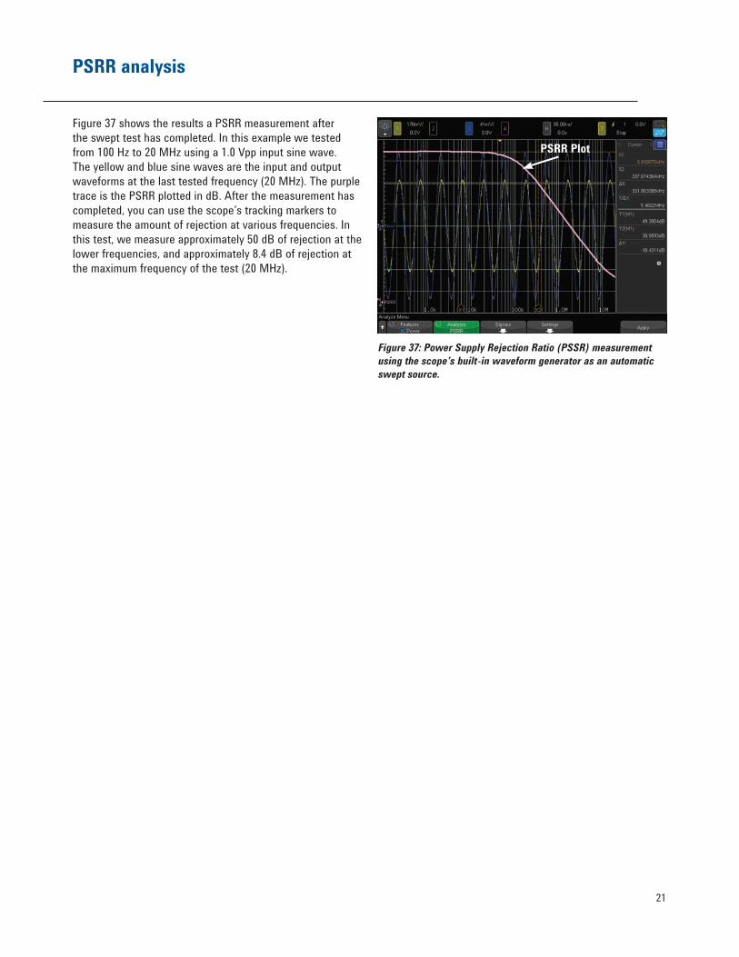
Figure 37: Power Supply Rejection Ratio (PSSR) measurement using the scope’s built-in waveform generator as an automatic swept source.
Figure 37 shows the results a PSRR measurement after the swept test has completed. In this example we tested from 100 Hz to 20 MHz using a 1.0 Vpp input sine wave. The yellow and blue sine waves are the input and output waveforms at the last tested frequency (20 MHz). The purple trace is the PSRR plotted in dB. After the measurement has completed, you can use the scope’s tracking markers to measure the amount of rejection at various frequencies. In this test, we measure approximately 50 dB of rejection at the lower frequencies, and approximately 8.4 dB of rejection at the maximum frequency of the test (20 MHz).
PSRR analysis
PSRR Plot
22
Efficiency analysis
Efficiency analysis measures the input real power and output power in order to compute the efficiency of your power supply (Efficiency = Pwr(out)/Pwr(in) x 100). Performing this measurement requires three active probes that require power (high-voltage differential active probe plus two active current probes). If two current probes are not available, then this measurement can be performed in a 2-step process: measure Input Power, measure Output Power, then compute efficiency. But let’s first show how to perform this measurement using two current probes in just one step.
1. If using Agilent’s SMPS training kit, set the S2 load switch to the ON position (high-load, maximum current). 2. Press the [Analyze] front panel key; then select the Power Application under the Features softkey. 3. Press the Analysis softkey; then select the Efficiency measurement. 4. Press the Signals softkey; then scroll to the bottom of the connections diagram. 5. Connect the N2790A high-voltage differential active probe between the scope’s channel-1 input to Line (red lead) and Neutral (black lead) as illustrated in the on-screen connections diagram shown in Figure 38. If using Agilent’s SMPS training kit, connect to TP2 (red lead) and TP1 (black lead). 6. Connect a current probe between the scope’s channel-2 input to the input Line current loop. If using Agilent’s SMPS training kit, connect to the J1 current loop in the direction indicated. 7. Connect a standard 10:1 passive voltage probe between the scope’s channel-3 input to the DC output signal. If using Agilent’s power demo board, connect to TP5 (probe tip grabber) and TP6 (ground). 8. If using an Agilent 4000 and 6000 X-Series oscilloscope, connect another current probe between the scope’s channel-4 input to the output DC current loop. If using Agilent’s SMPS training kit, connect to the J3 current loop in the direction indicated. If using an Agilent 3000 X-Series oscilloscope, you must use a second current probe that receives power from an external source since this scope can only power two active probes. 9. Press the Input V softkey; then set to 1 (channel-1). 10. Press the Input I softkey; then set to 2 (channel-2). 11. Press the Output V softkey; then set to 3 (channel-3). 12. Press the Output I softkey; then set to 4 (channel-4). 13. Press the AutoSetup softkey; then press Apply.
Your scope’s display should now look similar to Figure 39. Agilent’s SMPS training kit power supply measured an approximate efficiency of just 76% in this example.
Figure 38: Efficiency measurement connections diagram in the Signals menu.
Figure 39: Power Efficiency measurement results. .
23
Agilent Technologies OscilloscopesMultiple form factors from 20 MHz to > 90 GHz | Industry leading specs | Powerful applications
If two current probes are not available for this measurement, then follow the above procedure to measure the Input Power with your current probe connected between channel-2 and the input current loop. Connect nothing to the scope’s channel-4 input. After performing the above procedure, take note of the Input Power results, but ignore the Output Power and Efficiency measurements.
Next, move the current probe that is connected to the scope’s channel-2 input to channel-4. Then connect it to the output DC current loop (J3 if using Agilent’s SMPS training kit). Manually reposition and rescale channel-3 (V out) and channel-4 until both DC traces can be observed on-screen. Now take note of the Output Power results. Efficiency = Pwr-out/Pwr-in x 100%.
Publication title Publication type Publication numberInfiniiVision 6000 X-Series Oscilloscopes Data sheet 5991-4087ENInfiniiVision 4000 X-Series Oscilloscopes Data sheet 5991-1103ENInfiniiVision 3000 X-Series Oscilloscopes Data sheet 5990-6619ENDSOX3PWR/DSPX4PWR/DSOX6PWR Power Measurements Option Data sheet 5990-8869EN InfiniiVision Oscilloscope Probes & Accessories Data sheet 5968-8153ENN2790A 100-MHz, N2791A 25-MHz, N2891A 70-MHz Differential Active Probes Data sheet 5990-3780ENN2870A Series Passive Probes and Accessories Data sheet 5990-3930EN
To download these documents, insert the publication number in the URL: http://cp.literature.agilent.com/litweb/pdf/xxxx-xxxxEN.pdf
Product web site For the most up-to-date and complete application and product information, please visit our product Web site at: www.agilent.com/find/InfiniiVision
Related literature
Efficiency analysis
myAgilent
myAgilent
www.agilent.com/find/myagilentA personalized view into the information most relevant to you.
www.axiestandard.org
AdvancedTCA® Extensions for Instrumentation and Test (AXIe) is an open standard that extends the AdvancedTCA for general purpose and semiconductor test. Agilent is a founding member of the AXIe consortium.
www.lxistandard.org
LAN eXtensions for Instruments puts the power of Ethernet and the Web inside your test systems. Agilent is a founding member of the LXI consortium.
www.pxisa.org
PCI eXtensions for Instrumentation (PXI) modular instrumentation delivers a rugged, PC-based high-performance measurement and automation system.
Three-Year Warranty
www.agilent.com/find/ThreeYearWarrantyBeyond product specification, changing the ownership experience.Agilent is the only test and measurement company that offers three-year warranty on all instruments, worldwide.
Agilent Assurance Plans
www.agilent.com/find/AssurancePlansFive years of protection and no budgetary surprises to ensure your instruments are operating to specifications and you can continually rely on accurate measurements.
www.agilent.com/quality
Agilent Electronic Measurement GroupDEKRA Certified ISO 9001:2008 Quality Management System
Agilent Channel Partners
www.agilent.com/find/channelpartnersGet the best of both worlds: Agilent’s measurement expertise and product breadth, combined with channel partner convenience.
For more information on Agilent Technologies’ products, applications or services, please contact your local Agilent office. The complete list is available at:www.agilent.com/find/contactus