Page 1
RT9451®
DS9451-01 March 2017 www.richtek.com1
©Copyright 2017 Richtek Technology Corporation. All rights reserved. is a registered trademark of Richtek Technology Corporation.
Switch-Mode Single Cell Li-ion Battery Charger with USB OTG
General Description
The RT9451 integrates a high efficiency USB friendly switch
mode charger with On-The-Go (OTG) support for single
cell Li-ion and Li-polymer batteries, D+D− detection, and
a 50mA LDO regulator into a single chip.
The charger features a synchronous 375kHz PWM
controller with integrated power MOSFETs, input current
sensing and regulation, Minimum Input Voltage Regulation
(MIVR), high accuracy charge current and voltage
regulation, and charge termination. It charges the battery
in three phases : low current pre-charge, constant current
fast charge, and constant voltage trickle charge. The input
current is automatically limited to the value set by the
host. The charger can be configured to terminate charge
based on user-selectable minimum current level and
automatically restart the charge cycle if the battery voltage
falls below the recharge threshold. A safety timer with
reset control provides a safety backup for I2C interface.
The charger automatically enters sleep mode or high
impedance mode when the input supply is removed. The
charge status is reported to the host using the I2C interface
and the STAT pin. The D+D− detection circuit allows
automatic detection of a USB wall charger. If a wall charger
is detected, the input current limit will automatically
increase from 500mA to 975mA.
In OTG mode, the PWM controller boosts the battery
voltage to 5V and provides up to 1.6A of current to the
USB output. At very light load, the Boost operates in burst
mode to optimize efficiency. OTG mode can be enabled
either through I2C interface or GPIO control.
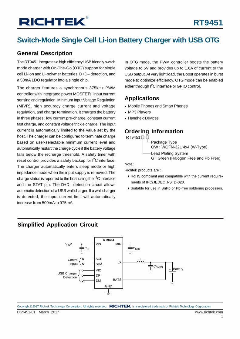
Simplified Application Circuit
RT9451
+ Battery
BATS
LX
VINVINCIN
CSYSS
L
MIDCMID
GND
DP
VIO
DM
SDA
SCLControl Inputs
USB Charger Detection
Ordering Information
Note :
Richtek products are :
RoHS compliant and compatible with the current require-
ments of IPC/JEDEC J-STD-020.
Suitable for use in SnPb or Pb-free soldering processes.
Applications Mobile Phones and Smart Phones
MP3 Players
Handheld Devices
RT9451Package TypeQW : WQFN-32L 4x4 (W-Type)
Lead Plating SystemG : Green (Halogen Free and Pb Free)
Page 2
RT9451
2
DS9451-01 March 2017www.richtek.com
©Copyright 2017 Richtek Technology Corporation. All rights reserved. is a registered trademark of Richtek Technology Corporation.
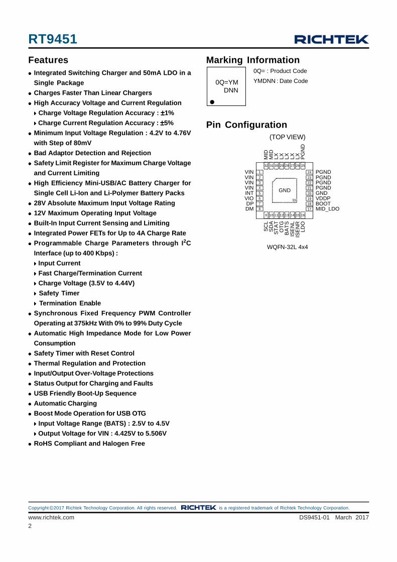
Pin Configuration
WQFN-32L 4x4
(TOP VIEW)
VIN
VINVINVIN
PGND
PGNDPGNDPGND
SD
AS
TA
TO
TG
BA
TS
MID
LX LX LX
VIOINT
VDDPGND
SC
LM
ID
ISE
NL
LX
DP BOOT
ISE
NR
LXLD
OP
GN
D
DM MID_LDO
33
24
23
22
21
1
2
3
4
10 11 12 13
31 30 29 28
20
19
5
6
9
32
14
27
187
15
26
16
25
178
GND
Features Integrated Switching Charger and 50mA LDO in a
Single Package
Charges Faster Than Linear Chargers
High Accuracy Voltage and Current Regulation
Charge Voltage Regulation Accuracy : ±±±±±1%
Charge Current Regulation Accuracy : ±±±±±5%
Minimum Input Voltage Regulation : 4.2V to 4.76V
with Step of 80mV
Bad Adaptor Detection and Rejection
Safety Limit Register for Maximum Charge Voltage
and Current Limiting
High Efficiency Mini-USB/AC Battery Charger for
Single Cell Li-Ion and Li-Polymer Battery Packs
28V Absolute Maximum Input Voltage Rating
12V Maximum Operating Input Voltage
Built-In Input Current Sensing and Limiting
Integrated Power FETs for Up to 4A Charge Rate
Programmable Charge Parameters through I2C
Interface (up to 400 Kbps) :
Input Current
Fast Charge/Termination Current
Charge Voltage (3.5V to 4.44V)
Safety Timer
Termination Enable
Synchronous Fixed Frequency PWM Controller
Operating at 375kHz With 0% to 99% Duty Cycle
Automatic High Impedance Mode for Low Power
Consumption
Safety Timer with Reset Control
Thermal Regulation and Protection
Input/Output Over-Voltage Protections
Status Output for Charging and Faults
USB Friendly Boot-Up Sequence
Automatic Charging
Boost Mode Operation for USB OTG
Input Voltage Range (BATS) : 2.5V to 4.5V
Output Voltage for VIN : 4.425V to 5.506V
RoHS Compliant and Halogen Free
Marking Information
0Q=YMDNN
0Q= : Product Code
YMDNN : Date Code
Page 3
RT9451
3
DS9451-01 March 2017 www.richtek.com
©Copyright 2017 Richtek Technology Corporation. All rights reserved. is a registered trademark of Richtek Technology Corporation.
Functional Pin DescriptionPin No. Pin Name Pin Function
1 to 4 VIN Power input. Bypass to PGND with a 10F ceramic capacitor. It also provides power to the load in boost mode.
5 INT Interrupt pin (open-drain). This pin is pulled low when a fault occurs.
6 VIO I/O reference voltage. A VIO level above 0.6V disables automatic D+/D detection.
7 DP USB port D+ input connection.
8 DM USB port D input connection.
9 SCL I2C interface clock input. Open-drain output, connect a 10k pull-up resistor.
10 SDA I2C interface data input. Open-drain output, connect a 10k pull-up resistor.
11 STAT Charge status indicator. Pull low when charge is in progress. Open-drain for other conditions. This pin can also be controlled through I2C register. The STAT
can be used to drive a LED or communicate with a host processor.
12 OTG Boost mode enable control. Boost mode is turned on whenever this pin is active. Polarity is user defined through I2C register. The pin is disabled by default and can be enabled through I2C register bit.
13 BATS Auxiliary power supply. Connect to the battery pack to provide power in high impedance mode. Bypass to GND with a 1F ceramic capacitor.
14 ISENL Charge current sense input. Battery current is sensed via the voltage drop across an external sense resistor. A 0.1F ceramic capacitor to PGND is required.
15 ISENR Battery voltage and current sense input. Bypass to PGND with a ceramic capacitor (minimum 0.1F) if there are long inductive leads to battery.
16 LDO LDO output. LDO is regulated to 4.9V and drives 60mA of current. Bypass LDO to GND with a minimum 1F ceramic capacitor. LDO is enabled when VIN is above the VIN UVLO threshold.
17 MID_LDO LDO input voltage. Please connect to MID.
18 BOOT Bootstrap supply for high-side gate driver. Connect a 100nF ceramic capacitor (voltage rating above 10V) from BOOT pin to LX pin.
19 VDDP Internal bias regulator voltage for driver. Connect a 1F ceramic capacitor from this output to PGND. External loads on VDDP is not allowed.
20, 33 (Exposed Pad)
GND Pure ground. The exposed pad must be soldered to a large PCB and connected to GND for maximum thermal dissipation.
21 to 25 PGND Power ground.
26 to 30 LX Switch node.
31, 32 MID Connection point between reverse blocking MOSFET and high-side MOSFET. Bypass to PGND with a minimum of 10F capacitor. No other circuits are recommended to connect at MID pin.
Page 4
RT9451
4
DS9451-01 March 2017www.richtek.com
©Copyright 2017 Richtek Technology Corporation. All rights reserved. is a registered trademark of Richtek Technology Corporation.
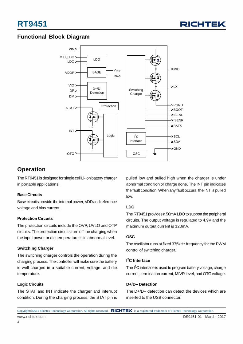
Functional Block Diagram
Operation
The RT9451 is designed for single cell Li-Ion battery charger
in portable applications.
Base Circuits
Base circuits provide the internal power, VDD and reference
voltage and bias current.
Protection Circuits
The protection circuits include the OVP, UVLO and OTP
circuits. The protection circuits turn off the charging when
the input power or die temperature is in abnormal level.
Switching Charger
The switching charger controls the operation during the
charging process. The controller will make sure the battery
is well charged in a suitable current, voltage, and die
temperature.
Logic Circuits
The STAT and INT indicate the charger and interrupt
condition. During the charging process, the STAT pin is
pulled low and pulled high when the charger is under
abnormal condition or charge done. The INT pin indicates
the fault condition. When any fault occurs, the INT is pulled
low.
LDO
The RT9451 provides a 50mA LDO to support the peripheral
circuits. The output voltage is regulated to 4.9V and the
maximum output current is 120mA.
OSC
The oscillator runs at fixed 375kHz frequency for the PWM
control of switching charger.
I2C Interface
The I2C interface is used to program battery voltage, charge
current, termination current, MIVR level, and OTG voltage.
D+/D−−−−− Detection
The D+/D− detection can detect the devices which are
inserted to the USB connector.
D+/D-Detection
SwitchingCharger
LDO
BASE
OSC
Protection
Logic I2C
Interface
VREF
IBIASVDDP
ISENL
BATS
ISENR
PGNDSTAT
LX
LDO
VIN
DP
VIO
SDA
DM
SCL
MID
OTG
INT
MID_LDO
GND
BOOT
Page 5
RT9451
5
DS9451-01 March 2017 www.richtek.com
©Copyright 2017 Richtek Technology Corporation. All rights reserved. is a registered trademark of Richtek Technology Corporation.
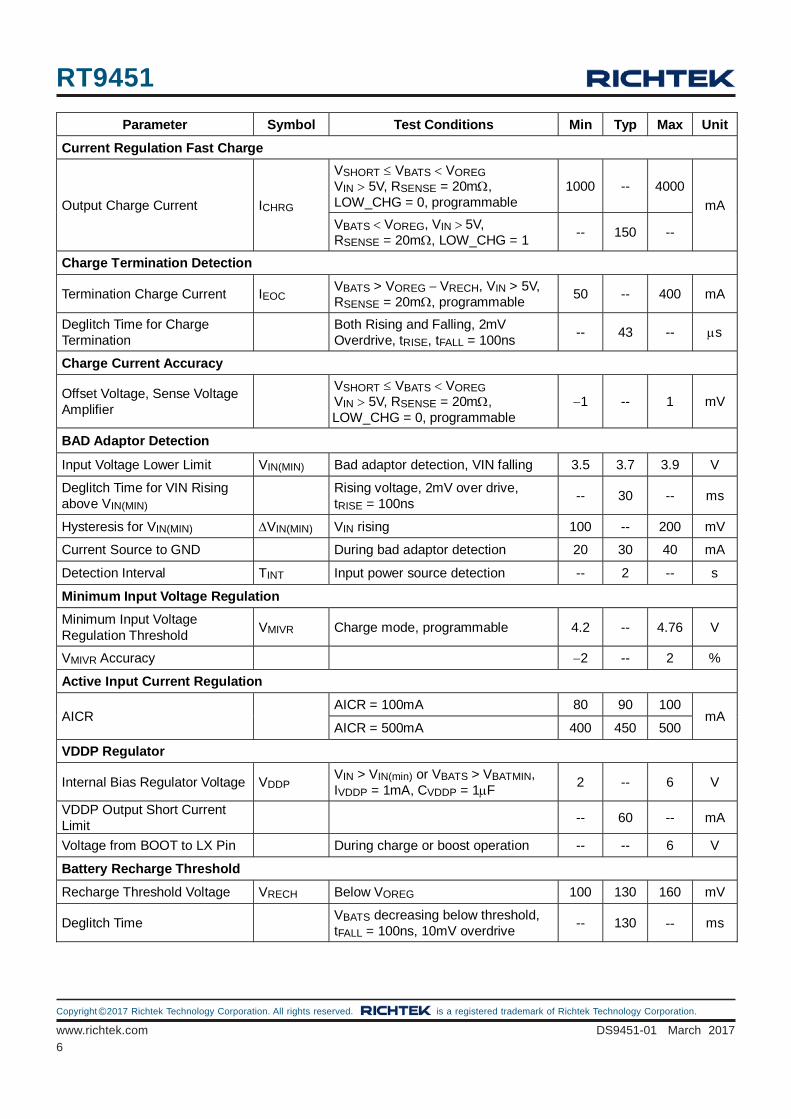
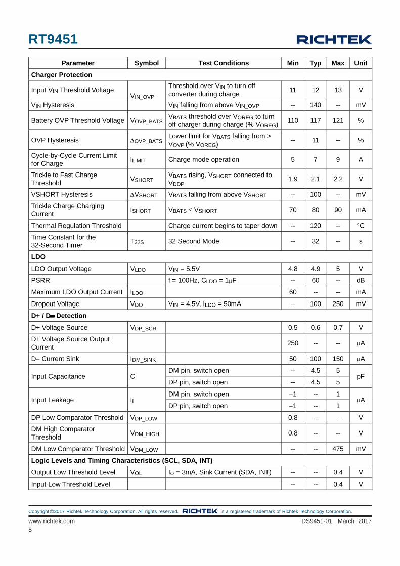
Electrical Characteristics
Parameter Symbol Test Conditions Min Typ Max Unit
Input Currents
Battery Discharge Current in
High Impedance Mode (ISENL, ISENR, LX, BATS Pins)
IDISCHARGE VBATS = 4.2 V High impedance mode, SDA = SCL = 0
-- 2 30 A
VIN Supply Current IQ VIN > VIN(MIN) Charger PWM ON -- 10000 --
A Charger PWM OFF -- -- 5000
Voltage Regulation
Output Charge Voltage VOREG Operating in voltage regulation, programmable
3.5 -- 4.44 V
Voltage Regulation Accuracy
0 to 85°C 1 -- 1 %
Recommended Operating Conditions (Note 4)
Supply Input Voltage Range, VIN -------------------------------------------------------------------------------------- 4.3V to 12V
Junction Temperature Range ------------------------------------------------------------------------------------------- −40°C to 125°C Ambient Temperature Range ------------------------------------------------------------------------------------------- −40°C to 85°C
Absolute Maximum Ratings (Note 1)
Supply Voltage VIN ------------------------------------------------------------------------------------------------------- −0.3V to 28V
MID, BOOT to PGND ---------------------------------------------------------------------------------------------------- −0.3V to 28V
Other Pins ------------------------------------------------------------------------------------------------------------------ −0.3V to 6V
VISENL to VISENR ----------------------------------------------------------------------------------------------------------- ±6V
Output Current (average) LX -------------------------------------------------------------------------------------------- 4A
Output Current (continuous) LDO ------------------------------------------------------------------------------------- 100mA
Power Dissipation, PD @ TA = 25°C
WQFN-32L 4x4 ------------------------------------------------------------------------------------------------------------ 3.59W
Package Thermal Resistance (Note 2)
WQFN-32L 4x4, θJA ------------------------------------------------------------------------------------------------------ 27.8°C/W
WQFN-32L 4x4, θJC ------------------------------------------------------------------------------------------------------ 7°C/W
Junction Temperature ---------------------------------------------------------------------------------------------------- 150°C Lead Temperature (Soldering, 10 sec.) ------------------------------------------------------------------------------ 260°C Storage Temperature Range -------------------------------------------------------------------------------------------- −65°C to 150°C ESD Susceptibility (Note 3)
HBM (Human Body Model) --------------------------------------------------------------------------------------------- 2kV
MM (Machine Model) ----------------------------------------------------------------------------------------------------- 200V
(VBATS = 3.6V ± 5%, TA = 25°C, unless otherwise specified)
Page 6
RT9451
6
DS9451-01 March 2017www.richtek.com
©Copyright 2017 Richtek Technology Corporation. All rights reserved. is a registered trademark of Richtek Technology Corporation.
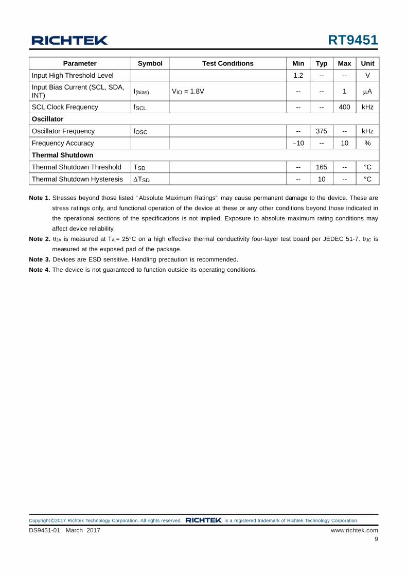
Parameter Symbol Test Conditions Min Typ Max Unit
Current Regulation Fast Charge
Output Charge Current ICHRG
VSHORT VBATS VOREG VIN 5V, RSENSE = 20m, LOW_CHG = 0, programmable
1000 -- 4000
mA
VBATS VOREG, VIN 5V, RSENSE = 20m, LOW_CHG = 1
-- 150 --
Charge Termination Detection
Termination Charge Current IEOC VBATS > VOREG VRECH, VIN > 5V, RSENSE = 20m, programmable
50 -- 400 mA
Deglitch Time for Charge Termination
Both Rising and Falling, 2mV Overdrive, tRISE, tFALL = 100ns
-- 43 -- s
Charge Current Accuracy
Offset Voltage, Sense Voltage Amplifier
VSHORT VBATS VOREG VIN 5V, RSENSE = 20m, LOW_CHG = 0, programmable
1 -- 1 mV
BAD Adaptor Detection
Input Voltage Lower Limit VIN(MIN) Bad adaptor detection, VIN falling 3.5 3.7 3.9 V
Deglitch Time for VIN Rising above VIN(MIN)
Rising voltage, 2mV over drive, tRISE = 100ns
-- 30 -- ms
Hysteresis for VIN(MIN) VIN(MIN) VIN rising 100 -- 200 mV
Current Source to GND During bad adaptor detection 20 30 40 mA
Detection Interval TINT Input power source detection -- 2 -- s
Minimum Input Voltage Regulation
Minimum Input Voltage Regulation Threshold
VMIVR Charge mode, programmable 4.2 -- 4.76 V
VMIVR Accuracy 2 -- 2 %
Active Input Current Regulation
AICR AICR = 100mA 80 90 100
mA AICR = 500mA 400 450 500
VDDP Regulator
Internal Bias Regulator Voltage VDDP VIN > VIN(min) or VBATS > VBATMIN, IVDDP = 1mA, CVDDP = 1F
2 -- 6 V
VDDP Output Short Current Limit
-- 60 -- mA
Voltage from BOOT to LX Pin During charge or boost operation -- -- 6 V
Battery Recharge Threshold
Recharge Threshold Voltage VRECH Below VOREG 100 130 160 mV
Deglitch Time VBATS decreasing below threshold, tFALL = 100ns, 10mV overdrive
-- 130 -- ms
Page 7
RT9451
7
DS9451-01 March 2017 www.richtek.com
©Copyright 2017 Richtek Technology Corporation. All rights reserved. is a registered trademark of Richtek Technology Corporation.
Parameter Symbol Test Conditions Min Typ Max Unit
Stat Output
Low Level Output Saturation Voltage
IO = 10mA, Sink Current -- -- 0.4 V
High Level Leakage Current Voltage on STAT pin is 5V -- -- 1 A
Reverse Protection Comparator
Reverse Protection Threshold, VIN VBATS
VSLP 2.3V VBATS VOREG, VIN Falling 0 40 100 mV
Reverse Protection Exit Hysteresis
VSLP-EXIT 2.3V VBATS VOREG 40 100 200 mV
Deglitch Time for VIN Rising above VSLP + VSLPEXIT
Rising Voltage -- 30 -- ms
VIN UVLO
Under-Voltage Lockout Threshold
VUVLO VIN Rising 3.05 3.3 3.55 V
Under-Voltage Lockout Threshold Hysteresis
VUVLO VIN falling from above VUVLO 120 150 -- mV
PWM
Internal N-MOSFET On-Resistance
High-Side RDSON_UG AICR = None, from VIN to LX -- 80 160 m
Low-Side RDSON_LG from LX to PGND -- 60 120
Maximum Duty Cycle DMAX -- 99.5 -- %
Minimum Duty Cycle DMIN 0 -- -- %
Boost Mode Operation for VIN
Boost Output Voltage Accuracy 2.5V < VIN < 4.5V; Including line and load regulation over full temp range
5 -- 5 %
Maximum Output Current for Boost
VIN_B = 5V, 2.5V < VBATS < 4.5V 1600 -- -- mA
Cycle-by-Cycle Current Limit for Boost
VIN_B = 5V, 2.5V < VBATS < 4.5V 4 6 8 A
Over-Voltage Protection Threshold for Boost (VIN Pin)
VIN_BOVP Threshold over VIN to turn off converter during boost
5.6 6 6.3 V
Over-Voltage Protection Hysteresis
VIN_BOVP VIN falling from above VIN_BOVP -- 200 -- mV
Maximum Battery Voltage for Boost
VBATMAX VBATS rising edge during boost 4.5 4.75 5 V
Maximum Battery Voltage Hysteresis
VBATMAX VBATS falling from above VBATMAX -- 200 -- mV
Minimum Battery Voltage for Boost (BATS pin)
VBATMIN During boosting -- 2.5 --
V Before boost Starts -- 2.9 3.05
Page 8
RT9451
8
DS9451-01 March 2017www.richtek.com
©Copyright 2017 Richtek Technology Corporation. All rights reserved. is a registered trademark of Richtek Technology Corporation.
Parameter Symbol Test Conditions Min Typ Max Unit
Charger Protection
Input VIN Threshold Voltage VIN_OVP
Threshold over VIN to turn off converter during charge
11 12 13 V
VIN Hysteresis VIN falling from above VIN_OVP -- 140 -- mV
Battery OVP Threshold Voltage VOVP_BATS VBATS threshold over VOREG to turn off charger during charge (% VOREG)
110 117 121 %
OVP Hysteresis OVP_BATS Lower limit for VBATS falling from > VOVP (% VOREG)
-- 11 -- %
Cycle-by-Cycle Current Limit for Charge
ILIMIT Charge mode operation 5 7 9 A
Trickle to Fast Charge Threshold
VSHORT VBATS rising, VSHORT connected to VDDP
1.9 2.1 2.2 V
VSHORT Hysteresis VSHORT VBATS falling from above VSHORT -- 100 -- mV
Trickle Charge Charging Current
ISHORT VBATS VSHORT 70 80 90 mA
Thermal Regulation Threshold Charge current begins to taper down -- 120 -- C
Time Constant for the 32-Second Timer
T32S 32 Second Mode -- 32 -- s
LDO
LDO Output Voltage VLDO VIN = 5.5V 4.8 4.9 5 V
PSRR f = 100Hz, CLDO = 1F -- 60 -- dB
Maximum LDO Output Current ILDO 60 -- -- mA
Dropout Voltage VDO VIN = 4.5V, ILDO = 50mA -- 100 250 mV
D+ / D Detection
D+ Voltage Source VDP_SCR 0.5 0.6 0.7 V
D+ Voltage Source Output Current
250 -- -- A
D Current Sink IDM_SINK 50 100 150 A
Input Capacitance CI DM pin, switch open -- 4.5 5
pF DP pin, switch open -- 4.5 5
Input Leakage II DM pin, switch open 1 -- 1
A DP pin, switch open 1 -- 1
DP Low Comparator Threshold VDP_LOW 0.8 -- -- V
DM High Comparator Threshold
VDM_HIGH 0.8 -- -- V
DM Low Comparator Threshold VDM_LOW -- -- 475 mV
Logic Levels and Timing Characteristics (SCL, SDA, INT)
Output Low Threshold Level VOL IO = 3mA, Sink Current (SDA, INT) -- -- 0.4 V
Input Low Threshold Level -- -- 0.4 V
Page 9
RT9451
9
DS9451-01 March 2017 www.richtek.com
©Copyright 2017 Richtek Technology Corporation. All rights reserved. is a registered trademark of Richtek Technology Corporation.
Parameter Symbol Test Conditions Min Typ Max Unit
Input High Threshold Level 1.2 -- -- V
Input Bias Current (SCL, SDA, INT)
I(bias) VIO = 1.8V -- -- 1 A
SCL Clock Frequency fSCL -- -- 400 kHz
Oscillator
Oscillator Frequency fOSC -- 375 -- kHz
Frequency Accuracy 10 -- 10 %
Thermal Shutdown
Thermal Shutdown Threshold TSD -- 165 -- °C
Thermal Shutdown Hysteresis TSD -- 10 -- °C
Note 1. Stresses beyond those listed “Absolute Maximum Ratings” may cause permanent damage to the device. These are
stress ratings only, and functional operation of the device at these or any other conditions beyond those indicated in
the operational sections of the specifications is not implied. Exposure to absolute maximum rating conditions may
affect device reliability.
Note 2. θJA is measured at TA = 25°C on a high effective thermal conductivity four-layer test board per JEDEC 51-7. θJC is
measured at the exposed pad of the package.
Note 3. Devices are ESD sensitive. Handling precaution is recommended.
Note 4. The device is not guaranteed to function outside its operating conditions.
Page 10
RT9451
10
DS9451-01 March 2017www.richtek.com
©Copyright 2017 Richtek Technology Corporation. All rights reserved. is a registered trademark of Richtek Technology Corporation.
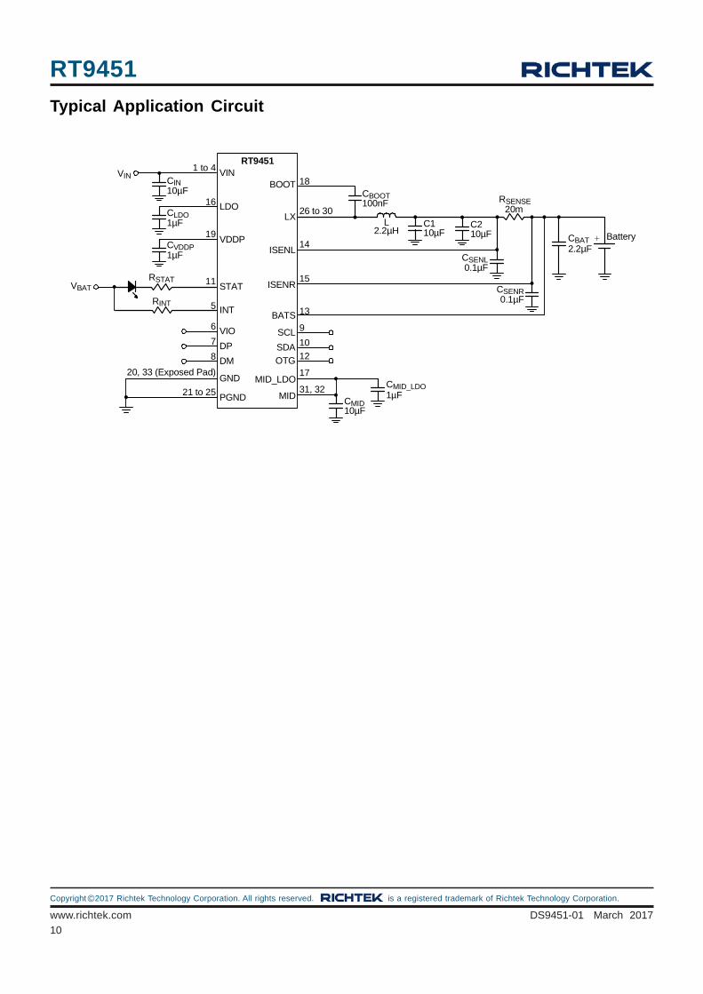
Typical Application Circuit
RT9451
26 to 30
10µF 10µF
100nF
2.2µH+ BatteryVDDP
ISENL
BATS
ISENRSTAT
LXLDO
VIN
DP
VIO
BOOT
INT
18
20m
CSENL
14
15
13
VIN
10µF
1 to 4
16
19
VBAT11
5
6
7
20, 33 (Exposed Pad)
CIN
1µFCLDO
1µFCVDDP
DM8
RSTAT
RINT
0.1µF
CSENR0.1µF
RSENSE
C1 C2L
CBOOT
SDA
SCL10
9
MID
10µF
31, 32CMID
MID_LDO
1µF
17CMID_LDO
OTG 12
PGND
GND
21 to 25
2.2µFCBAT
Page 11
RT9451
11
DS9451-01 March 2017 www.richtek.com
©Copyright 2017 Richtek Technology Corporation. All rights reserved. is a registered trademark of Richtek Technology Corporation.
Typical Operating CharacteristicsCharge Mode
Efficiency vs. Battery Voltage
60
65
70
75
80
85
90
95
100
3.4 3.5 3.6 3.7 3.8 3.9 4 4.1 4.2
Battery Voltage (V)
Effi
cie
ncy
(%
)
VIN = 5V
ICHRG = 1AICHRG = 1.4AICHRG = 1.8AICHRG = 2.2AICHRG = 2.6AICHRG = 3A
Efficiency vs. Battery Voltage
60
65
70
75
80
85
90
95
100
3.4 3.5 3.6 3.7 3.8 3.9 4 4.1 4.2
Battery Voltage (V)
Effi
cie
ncy
(%
)
VIN = 9V
ICHRG = 1AICHRG = 1.4AICHRG = 1.8AICHRG = 2.2AICHRG = 2.6AICHRG = 3A
Time (10ms/Div)
Adapter Insertion
LX(10V/Div)
IIN(200mA/Div)
VIN = 5V, VBAT = 3.7V
STAT(2V/Div)
VIN(5V/Div)
Time (5ms/Div)
Battery Removal
LX(5V/Div)
ILX(1A/Div)
VIN = 5V, VBAT = 3.7V, TERM_EN = 1
STAT(2V/Div)
VBAT(1V/Div)
Time (10ms/Div)
Bad Adapter
IIN(20mA/Div)
INT(5V/Div)
VIN = 5V/10mA, VBAT = 3.7V
VIN(5V/Div)
Time (250μs/Div)
Minimum Input Voltage Regulation
IIN(1A/Div)
INT(5V/Div)
VMIVR = 4.76V, VBAT = 3.7V
VIN(2V/Div)
VIN = 5V/1A, ICHRG = 2A,
No AICR
Page 12
RT9451
12
DS9451-01 March 2017www.richtek.com
©Copyright 2017 Richtek Technology Corporation. All rights reserved. is a registered trademark of Richtek Technology Corporation.
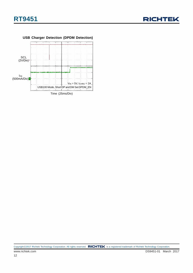
Time (25ms/Div)
USB Charger Detection (DPDM Detection)
IIN(500mA/Div)
SCL(2V/Div)
VIN = 5V, ICHRG = 2A
USB100 Mode, Short DP and DM Set DPDM_EN
Page 13
RT9451
13
DS9451-01 March 2017 www.richtek.com
©Copyright 2017 Richtek Technology Corporation. All rights reserved. is a registered trademark of Richtek Technology Corporation.
Boost Mode
Efficiency vs. Load Current
0
10
20
30
40
50
60
70
80
90
100
0 200 400 600 800 1000 1200 1400 1600 1800
Load Current (mA)
Effi
cie
ncy
(%
)
VIN = 5V
VBAT = 3.4VVBAT = 3.6VVBAT = 3.8VVBAT = 4VVBAT = 4.2V
Line Regulation
4.98
4.99
5.00
5.01
5.02
5.03
5.04
5.05
5.06
5.07
5.08
3.3 3.4 3.5 3.6 3.7 3.8 3.9 4 4.1 4.2 4.3
Battery Voltage (V)
Inp
ut V
olta
ge
(V
)
VIN = 5V
ILOAD = 0.1AILOAD = 0.4AILOAD = 0.7AILOAD = 1AILOAD = 1.3AILOAD = 1.6A
Load Regulation
4.98
4.99
5.00
5.01
5.02
5.03
5.04
5.05
5.06
5.07
5.08
0 200 400 600 800 1000 1200 1400 1600 1800
Load Current (mA)
Inp
ut V
olta
ge
(V
)
VIN = 5V
VBAT = 3.4VVBAT = 3.6VVBAT = 3.8VVBAT = 4VVBAT = 4.2V
Time (5ms/Div)
Battery Under-Voltage Protection
ILX(1A/Div)
VBAT(2V/Div)
INT(2V/Div)
VIN(5V/Div)
VIN = 5V, ILOAD = 500mA
Time (25μs/Div)
VIN Over-Voltage Protection
ILX(1A/Div)
INT(5V/Div)
VIN(5V/Div)
VIN = 5V, ILOAD = 0.5A, VBAT = 3.7V
Time (250μs/Div)
Load Transient Response
ILOAD(500mA/Div)
VIN_ac(100mV/Div)
ILOAD = 0.2A to 1A (30mA/μs)VIN = 5V, VBAT = 3.7V
Page 14
RT9451
14
DS9451-01 March 2017www.richtek.com
©Copyright 2017 Richtek Technology Corporation. All rights reserved. is a registered trademark of Richtek Technology Corporation.
Time (5s/Div)
32-Second Safety Timer
VIN(5V/Div)
ILX(200mA/Div)
VIN = 5V, VBAT = 3.7V, ILOAD = 0.2A
Without Timer Reset
Page 15
RT9451
15
DS9451-01 March 2017 www.richtek.com
©Copyright 2017 Richtek Technology Corporation. All rights reserved. is a registered trademark of Richtek Technology Corporation.
Application Information
The RT9451 is an integrated solution of single-cell Li-ion
and Li-polymer battery charger for portable applications.
The part integrates a synchronous PWM controller with
power MOSFETs to provide MIVR (Minimum Input Voltage
Regulation), input current sensing, high accuracy current
and voltage regulation, and charge termination in a small
package for space limited devices. The part also features
USB OTG (On-The-Go) function and USB charger detection
(DPDM detection) function.
The RT9451 provides three operation modes : charge
mode, boost mode (USB OTG), and high impedance mode.
In charge mode, the RT9451 supports a precision charging
system for single cell. In boost mode, the RT9451 works
as a Boost converter and boosts the voltage from battery
to VIN pin for sourcing the OTG devices. In high impedance
mode, the RT9451 stops charging or boosting and
operates in a mode with low quiescent current from VIN or
battery to reduce the power consumption when the
portable device is in standby mode.
In charge mode, the RT9451 integrates USB charger
detection for input current limit of 500mA and 1A. The
detection is automatically triggered after each POR. The
detection result can be ignored by the host via I2C interface.
The slave address for the RT9451 is“1001010”.
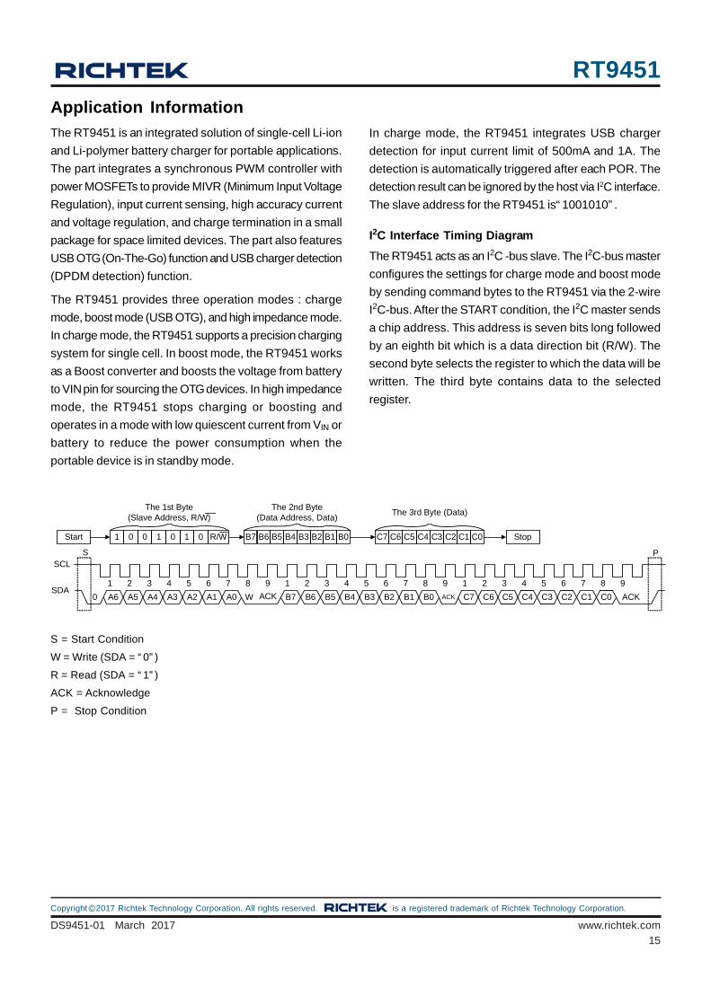
I2C Interface Timing Diagram
The RT9451 acts as an I2C -bus slave. The I2C-bus master
configures the settings for charge mode and boost mode
by sending command bytes to the RT9451 via the 2-wire
I2C-bus. After the START condition, the I2C master sends
a chip address. This address is seven bits long followed
by an eighth bit which is a data direction bit (R/W). The
second byte selects the register to which the data will be
written. The third byte contains data to the selected
register.
S = Start Condition
W = Write (SDA = “0”)
R = Read (SDA = “1”)
ACK = Acknowledge
P = Stop Condition
B7
1 2 3 4 5 6 7 8 9 1 2
B6 B2 B1 B0
3 4 5 6 7 8 9 1 2 3 4 5 6 7 8 9
C5 C4 C3 C2 C1 C0W ACK ACK
S P
0 B4 ACK
SCL
SDAA0A1A2A3A4A5A6 B5 C7 C6B3
Start 1 0 0 1 0 1 0 R/W B7 B6 B5 B4 B3 B2 B1 B0 C7 C6 C5 C4 C3 C2 C1 C0 Stop
The 2nd Byte (Data Address, Data)
The 3rd Byte (Data)The 1st Byte
(Slave Address, R/W)
Page 16
RT9451
16
DS9451-01 March 2017www.richtek.com
©Copyright 2017 Richtek Technology Corporation. All rights reserved. is a registered trademark of Richtek Technology Corporation.
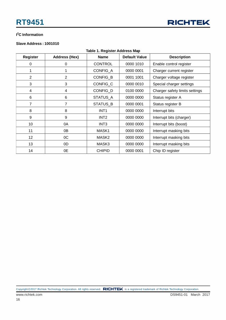
I2C Information
Slave Address : 1001010
Register Address (Hex) Name Default Value Description
0 0 CONTROL 0000 1010 Enable control register
1 1 CONFIG_A 0000 0001 Charger current register
2 2 CONFIG_B 0001 1001 Charger voltage register
3 3 CONFIG_C 0000 0010 Special charger settings
4 4 CONFIG_D 0100 0000 Charger safety limits settings
6 6 STATUS_A 0000 0000 Status register A
7 7 STATUS_B 0000 0001 Status register B
8 8 INT1 0000 0000 Interrupt bits
9 9 INT2 0000 0000 Interrupt bits (charger)
10 0A INT3 0000 0000 Interrupt bits (boost)
11 0B MASK1 0000 0000 Interrupt masking bits
12 0C MASK2 0000 0000 Interrupt masking bits
13 0D MASK3 0000 0000 Interrupt masking bits
14 0E CHIPID 0000 0001 Chip ID register
Table 1. Register Address Map
Page 17
RT9451
17
DS9451-01 March 2017 www.richtek.com
©Copyright 2017 Richtek Technology Corporation. All rights reserved. is a registered trademark of Richtek Technology Corporation.
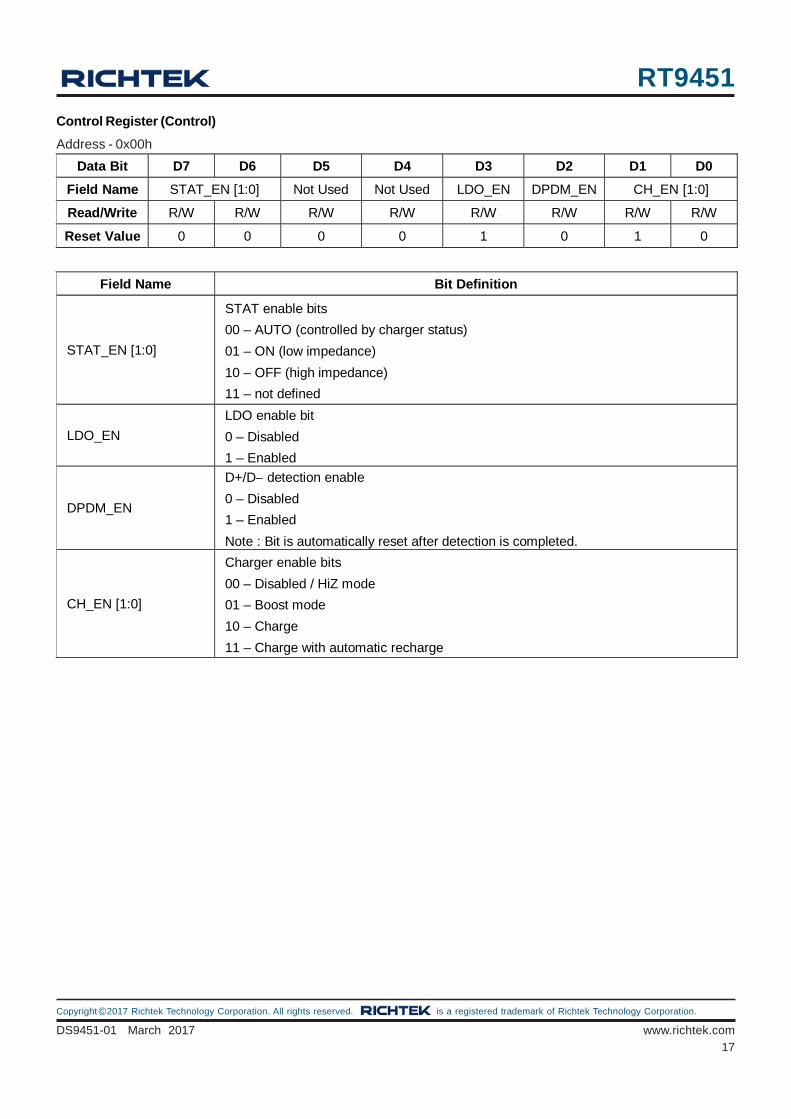
Control Register (Control)
Address - 0x00h
Data Bit D7 D6 D5 D4 D3 D2 D1 D0
Field Name STAT_EN [1:0] Not Used Not Used LDO_EN DPDM_EN CH_EN [1:0]
Read/Write R/W R/W R/W R/W R/W R/W R/W R/W
Reset Value 0 0 0 0 1 0 1 0
Field Name Bit Definition
STAT_EN [1:0]
STAT enable bits
00 – AUTO (controlled by charger status)
01 – ON (low impedance)
10 – OFF (high impedance)
11 – not defined
LDO_EN
LDO enable bit
0 – Disabled
1 – Enabled
DPDM_EN
D+/D detection enable
0 – Disabled
1 – Enabled
Note : Bit is automatically reset after detection is completed.
CH_EN [1:0]
Charger enable bits
00 – Disabled / HiZ mode
01 – Boost mode
10 – Charge
11 – Charge with automatic recharge
Page 18
RT9451
18
DS9451-01 March 2017www.richtek.com
©Copyright 2017 Richtek Technology Corporation. All rights reserved. is a registered trademark of Richtek Technology Corporation.
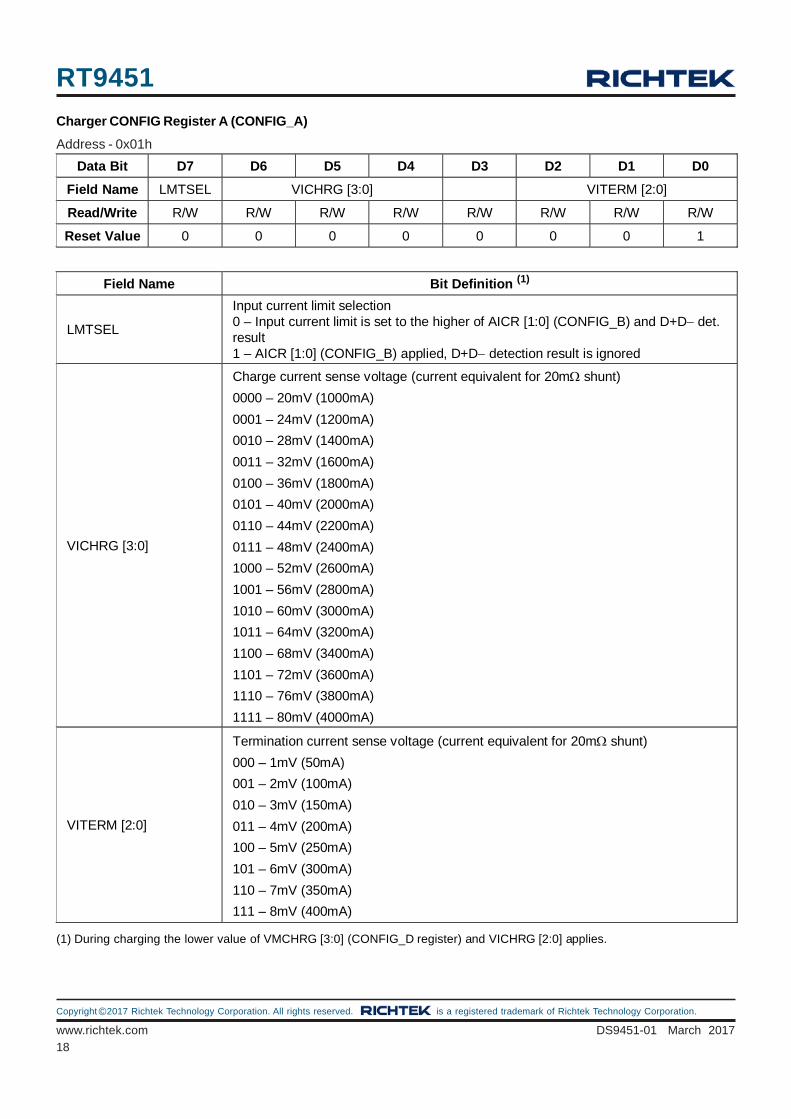
Charger CONFIG Register A (CONFIG_A)
Address - 0x01h
Data Bit D7 D6 D5 D4 D3 D2 D1 D0
Field Name LMTSEL VICHRG [3:0] VITERM [2:0]
Read/Write R/W R/W R/W R/W R/W R/W R/W R/W
Reset Value 0 0 0 0 0 0 0 1
Field Name Bit Definition (1)
LMTSEL
Input current limit selection 0 – Input current limit is set to the higher of AICR [1:0] (CONFIG_B) and D+D det. result 1 – AICR [1:0] (CONFIG_B) applied, D+D detection result is ignored
VICHRG [3:0]
Charge current sense voltage (current equivalent for 20m shunt)
0000 – 20mV (1000mA)
0001 – 24mV (1200mA)
0010 – 28mV (1400mA)
0011 – 32mV (1600mA)
0100 – 36mV (1800mA)
0101 – 40mV (2000mA)
0110 – 44mV (2200mA)
0111 – 48mV (2400mA)
1000 – 52mV (2600mA)
1001 – 56mV (2800mA)
1010 – 60mV (3000mA)
1011 – 64mV (3200mA)
1100 – 68mV (3400mA)
1101 – 72mV (3600mA)
1110 – 76mV (3800mA)
1111 – 80mV (4000mA)
VITERM [2:0]
Termination current sense voltage (current equivalent for 20m shunt)
000 – 1mV (50mA)
001 – 2mV (100mA)
010 – 3mV (150mA)
011 – 4mV (200mA)
100 – 5mV (250mA)
101 – 6mV (300mA)
110 – 7mV (350mA)
111 – 8mV (400mA)
(1) During charging the lower value of VMCHRG [3:0] (CONFIG_D register) and VICHRG [2:0] applies.
Page 19
RT9451
19
DS9451-01 March 2017 www.richtek.com
©Copyright 2017 Richtek Technology Corporation. All rights reserved. is a registered trademark of Richtek Technology Corporation.
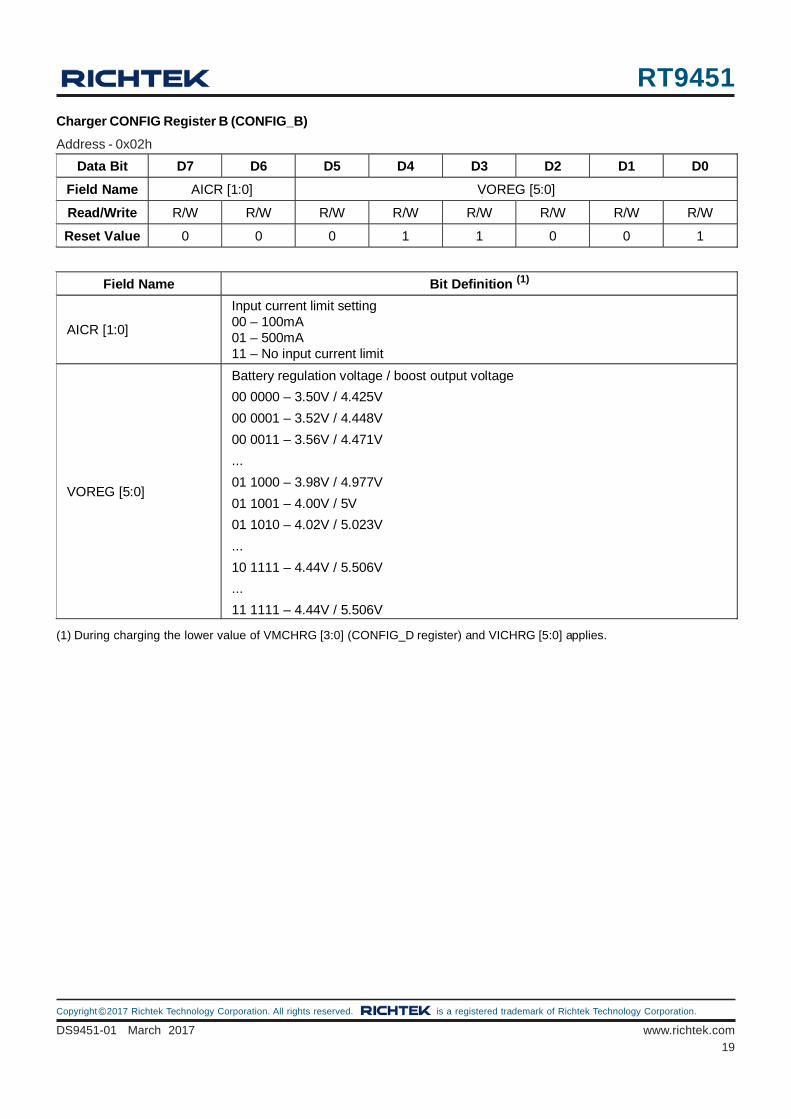
Charger CONFIG Register B (CONFIG_B)
Address - 0x02h
Data Bit D7 D6 D5 D4 D3 D2 D1 D0
Field Name AICR [1:0] VOREG [5:0]
Read/Write R/W R/W R/W R/W R/W R/W R/W R/W
Reset Value 0 0 0 1 1 0 0 1
Field Name Bit Definition (1)
AICR [1:0]
Input current limit setting 00 – 100mA 01 – 500mA 11 – No input current limit
VOREG [5:0]
Battery regulation voltage / boost output voltage
00 0000 – 3.50V / 4.425V
00 0001 – 3.52V / 4.448V
00 0011 – 3.56V / 4.471V
...
01 1000 – 3.98V / 4.977V
01 1001 – 4.00V / 5V
01 1010 – 4.02V / 5.023V
...
10 1111 – 4.44V / 5.506V
...
11 1111 – 4.44V / 5.506V
(1) During charging the lower value of VMCHRG [3:0] (CONFIG_D register) and VICHRG [5:0] applies.
Page 20
RT9451
20
DS9451-01 March 2017www.richtek.com
©Copyright 2017 Richtek Technology Corporation. All rights reserved. is a registered trademark of Richtek Technology Corporation.
Charger CONFIG Register C (CONFIG_C)
Address - 0x03h
Data Bit D7 D6 D5 D4 D3 D2 D1 D0
Field Name Not Used OTG_PL OTG_EN TERM_EN LOW_CHG MIVR [2:0]
Read/Write R/W R/W R/W R/W R/W R/W R/W R/W
Reset Value 0 0 0 0 0 0 1 0
Field Name Bit Definition
OTG_PL OTG pin polarity 0 – Active low 1 – Active high
OTG_EN OTG pin enable 0 – Pin is disabled 1 – Pin is enabled
TERM_EN Charge termination enable 0 – Disabled 1 – Enabled
LOW_CHG Low charge current enable bit (current equivalent for 20m shunt) 0 – Normal charge current sense voltage per register CONFIG_A 1 – 3mV (150mA)
MIVR [2:0]
Input voltage MIVR regulation voltage
000 – 4.20V
001 – 4.28V
010 – 4.36V
011 – 4.44V
100 – 4.52V
101 – 4.60V
110 – 4.68V
111 – 4.76V
Page 21
RT9451
21
DS9451-01 March 2017 www.richtek.com
©Copyright 2017 Richtek Technology Corporation. All rights reserved. is a registered trademark of Richtek Technology Corporation.
Charger CONFIG Register D (CONFIG_D)
Address - 0x04h
Data Bit D7 D6 D5 D4 D3 D2 D1 D0
Field Name VMCHRG [3:0] VMREG [3:0]
Read/Write R/W R/W R/W R/W R/W R/W R/W R/W
Reset Value 0 1 0 0 0 0 0 0
Field Name Bit Definition (1)
VMCHRG [3:0]
Maximum charge current sense voltage (current equivalent for 20m shunt) 0000 – 20mV (1000mA) 0001 – 24mV (1200mA) 0010 – 28mV (1400mA) 0011 – 32mV (1600mA) 0100 – 36mV (1800mA) 0101 – 40mV (2000mA) 0110 – 44mV (2200mA) 0111 – 48mV (2400mA) 1000 – 52mV (2600mA) 1001 – 56mV (2800mA) 1010 – 60mV (3000mA) 1011 – 64mV (3200mA) 1100 – 68mV (3400mA) 1101 – 72mV (3600mA) 1110 – 76mV (3800mA) 1111 – 80mV (4000mA)
VMREG [3:0]
Maximum Battery Regulation Voltage / Maximum OTG Regulation Voltage 0000 – 4.20V / 5.230V 0001 – 4.22V / 5.253V 0010 – 4.24V / 5.276V … 1100 – 4.44V / 5.506V ... 1111 – 4.44V / 5.506V
Page 22
RT9451
22
DS9451-01 March 2017www.richtek.com
©Copyright 2017 Richtek Technology Corporation. All rights reserved. is a registered trademark of Richtek Technology Corporation.
STATUS Register A (STATUS_A)
Address - 0x06h
Data Bit D7 D6 D5 D4 D3 D2 D1 D0
Field Name Not Used STANDBY Not Used CHSTAT [2:0] LDO Not Used
Read/Write R R R R R R R R
Reset Value 0 0 0 0 0 0 0 0
Field Name Bit Definition (1)
Not used N/A
STANDBY Standby status indicator 0 – Device is in ACTIVE mode 1 – Device is in STANDBY mode
Not used N/A
CHSTAT [2:0]
Charger status bit
000 – High impedance mode or ready to charge
001 – Charge in progress (fast charge)
010 – Charge done
011 – Boost mode
100 – Charge in progress (pre charge)
101 – Not defined
110 – Not defined
111 – Not defined
LDO LDO status bit 0 – LDO is disabled (OFF) 1 – LDO is enabled (ON), no fault
Not used N/A
(1) Default values reflect state after Power On Reset, no charger plugged in, no faults present.
Page 23
RT9451
23
DS9451-01 March 2017 www.richtek.com
©Copyright 2017 Richtek Technology Corporation. All rights reserved. is a registered trademark of Richtek Technology Corporation.
STATUS Register B (STATUS_B)
Address - 0x07h
Data Bit D7 D6 D5 D4 D3 D2 D1 D0
Field Name RESET Not used Not used Not used Not used DPDM_D DPDM_R OTG
Read/Write W R R R R R R R
Reset Value 0 0 0 0 0 0 0 1
Field Name Bit Definition (1)
RESET
Reset
0 – No effect
1 – Reset all parameters to default values
Note : Read always returns “0”
Not used N/A
Not used N/A
Not used N/A
Not used N/A
DPDM_D D+/D detection done bit 0 – DPDM detection in progress or not started after initial power up reset 1 – DPDM detection is complete
DPDM_R D+D detection result 0 – Standard USB port (500mA current limit) 1 – USB charger (975mA current limit)
OTG OTG pin status 0 – OTG pin at low level 1 – OTG pin at high level
(1) Default values reflect state after Power On Reset, no charger plugged in, no faults present, OTG pin high.
Page 24
RT9451
24
DS9451-01 March 2017www.richtek.com
©Copyright 2017 Richtek Technology Corporation. All rights reserved. is a registered trademark of Richtek Technology Corporation.
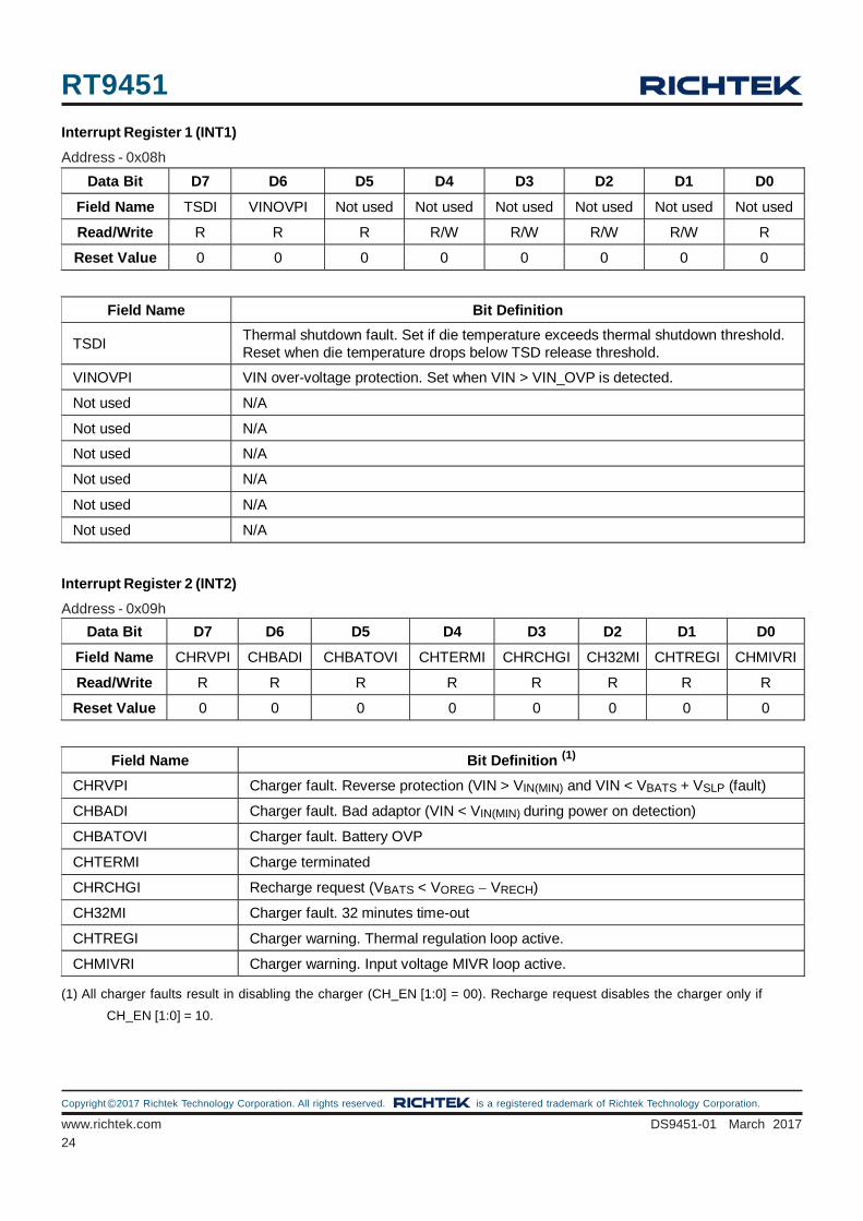
Interrupt Register 1 (INT1)
Address - 0x08h
Data Bit D7 D6 D5 D4 D3 D2 D1 D0
Field Name TSDI VINOVPI Not used Not used Not used Not used Not used Not used
Read/Write R R R R/W R/W R/W R/W R
Reset Value 0 0 0 0 0 0 0 0
Field Name Bit Definition
TSDI Thermal shutdown fault. Set if die temperature exceeds thermal shutdown threshold. Reset when die temperature drops below TSD release threshold.
VINOVPI VIN over-voltage protection. Set when VIN > VIN_OVP is detected.
Not used N/A
Not used N/A
Not used N/A
Not used N/A
Not used N/A
Not used N/A
Interrupt Register 2 (INT2)
Address - 0x09h
Data Bit D7 D6 D5 D4 D3 D2 D1 D0
Field Name CHRVPI CHBADI CHBATOVI CHTERMI CHRCHGI CH32MI CHTREGI CHMIVRI
Read/Write R R R R R R R R
Reset Value 0 0 0 0 0 0 0 0
Field Name Bit Definition (1)
CHRVPI Charger fault. Reverse protection (VIN > VIN(MIN) and VIN < VBATS + VSLP (fault)
CHBADI Charger fault. Bad adaptor (VIN < VIN(MIN) during power on detection)
CHBATOVI Charger fault. Battery OVP
CHTERMI Charge terminated
CHRCHGI Recharge request (VBATS < VOREG VRECH)
CH32MI Charger fault. 32 minutes time-out
CHTREGI Charger warning. Thermal regulation loop active.
CHMIVRI Charger warning. Input voltage MIVR loop active.
(1) All charger faults result in disabling the charger (CH_EN [1:0] = 00). Recharge request disables the charger only if
CH_EN [1:0] = 10.
Page 25
RT9451
25
DS9451-01 March 2017 www.richtek.com
©Copyright 2017 Richtek Technology Corporation. All rights reserved. is a registered trademark of Richtek Technology Corporation.
Interrupt Register 3 (INT3)
Address - 0x0Ah
Data Bit D7 D6 D5 D4 D3 D2 D1 D0
Field Name BSTVINOVI BSTOLI BSTLOWVI BSTBATOVI BST32SI Not
used Not
used Not
used
Read/Write R R R R R R R R
Reset Value 0 0 0 0 0 0 0 0
Field Name Bit Definition (1)
BSTVINOVI Boost fault. VIN OVP (VIN > VIN_BOVP)
BSTOLI Boost fault. Over load.
BSTLOWVI Boost fault. Battery voltage is too low.
BSTBATOVI Boost fault. Battery over voltage.
BST32SI Boost fault. 32s time-out fault.
Not used N/A
Not used N/A
Not used N/A
(1) All charger faults result in disabling the charger (CH_EN [1:0] = 00).
Interrupt MASK Register 1 (MASK1)
Address - 0x0Bh
Data Bit D7 D6 D5 D4 D3 D2 D1 D0
Field Name TSDM VINOVPM Not used Not used Not used Not used Not used Not used
Read/Write R/W R/W R/W R/W R/W R/W R/W R/W
Reset Value 0 0 0 0 0 0 0 0
Field Name Bit Definition (1)
TSDM TSD fault interrupt mask 0 – Interrupt not masked 1 – Interrupt masked
VINOVPM VIN OVP fault interrupt mask 0 – Interrupt not masked 1 – Interrupt masked
Not used N/A
Not used N/A
Not used N/A
Not used N/A
Not used N/A
Not used N/A
(1) Setting any of the interrupt mask bits does not disable protection circuits. When set, the respective fault will not be
signaled on the INT pin.
Page 26
RT9451
26
DS9451-01 March 2017www.richtek.com
©Copyright 2017 Richtek Technology Corporation. All rights reserved. is a registered trademark of Richtek Technology Corporation.
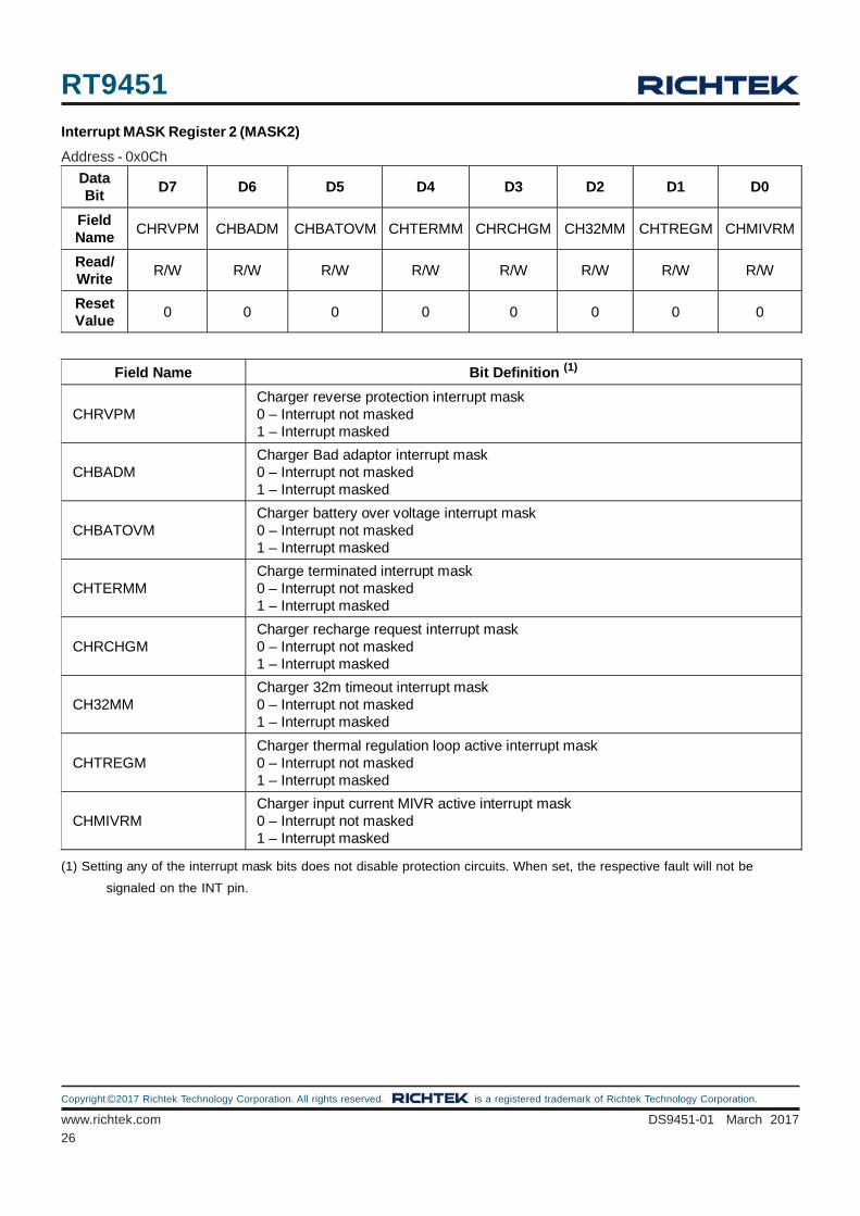
Interrupt MASK Register 2 (MASK2)
Address - 0x0Ch
Data Bit
D7 D6 D5 D4 D3 D2 D1 D0
Field Name
CHRVPM CHBADM CHBATOVM CHTERMM CHRCHGM CH32MM CHTREGM CHMIVRM
Read/Write
R/W R/W R/W R/W R/W R/W R/W R/W
Reset Value
0 0 0 0 0 0 0 0
Field Name Bit Definition (1)
CHRVPM Charger reverse protection interrupt mask 0 – Interrupt not masked 1 – Interrupt masked
CHBADM Charger Bad adaptor interrupt mask 0 – Interrupt not masked 1 – Interrupt masked
CHBATOVM Charger battery over voltage interrupt mask 0 – Interrupt not masked 1 – Interrupt masked
CHTERMM Charge terminated interrupt mask 0 – Interrupt not masked 1 – Interrupt masked
CHRCHGM Charger recharge request interrupt mask 0 – Interrupt not masked 1 – Interrupt masked
CH32MM Charger 32m timeout interrupt mask 0 – Interrupt not masked 1 – Interrupt masked
CHTREGM Charger thermal regulation loop active interrupt mask 0 – Interrupt not masked 1 – Interrupt masked
CHMIVRM Charger input current MIVR active interrupt mask 0 – Interrupt not masked 1 – Interrupt masked
(1) Setting any of the interrupt mask bits does not disable protection circuits. When set, the respective fault will not be
signaled on the INT pin.
Page 27
RT9451
27
DS9451-01 March 2017 www.richtek.com
©Copyright 2017 Richtek Technology Corporation. All rights reserved. is a registered trademark of Richtek Technology Corporation.
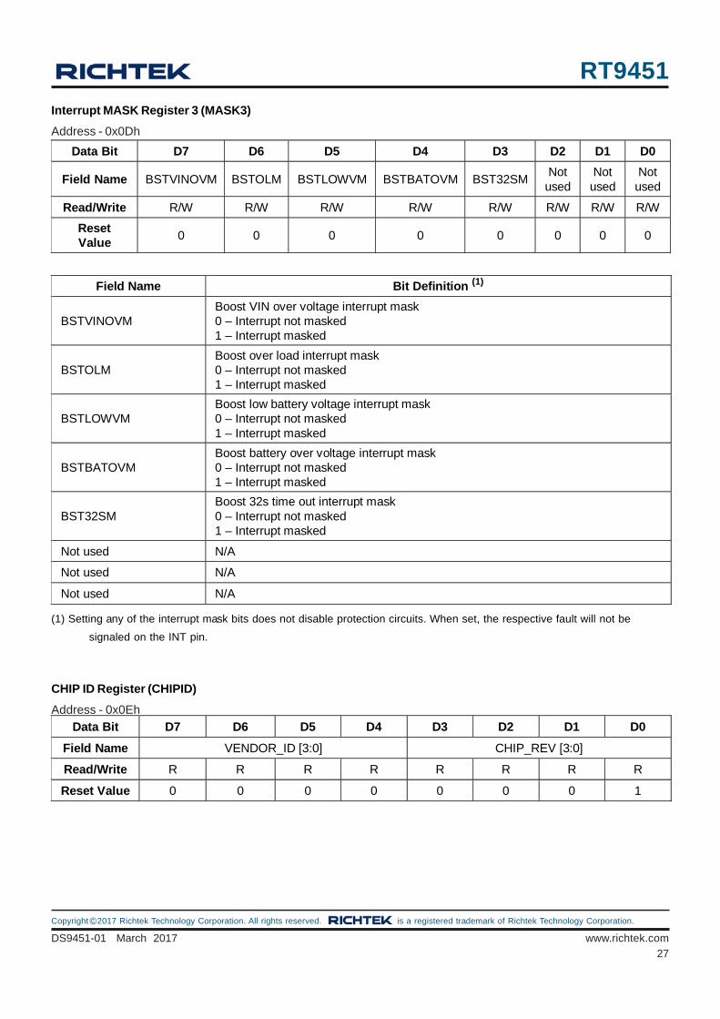
Interrupt MASK Register 3 (MASK3)
Address - 0x0Dh
Data Bit D7 D6 D5 D4 D3 D2 D1 D0
Field Name BSTVINOVM BSTOLM BSTLOWVM BSTBATOVM BST32SM Not
used Not
used Not
used
Read/Write R/W R/W R/W R/W R/W R/W R/W R/W
Reset Value
0 0 0 0 0 0 0 0
Field Name Bit Definition (1)
BSTVINOVM Boost VIN over voltage interrupt mask 0 – Interrupt not masked 1 – Interrupt masked
BSTOLM Boost over load interrupt mask 0 – Interrupt not masked 1 – Interrupt masked
BSTLOWVM Boost low battery voltage interrupt mask 0 – Interrupt not masked 1 – Interrupt masked
BSTBATOVM Boost battery over voltage interrupt mask 0 – Interrupt not masked 1 – Interrupt masked
BST32SM Boost 32s time out interrupt mask 0 – Interrupt not masked 1 – Interrupt masked
Not used N/A
Not used N/A
Not used N/A
(1) Setting any of the interrupt mask bits does not disable protection circuits. When set, the respective fault will not be
signaled on the INT pin.
CHIP ID Register (CHIPID)
Address - 0x0Eh
Data Bit D7 D6 D5 D4 D3 D2 D1 D0
Field Name VENDOR_ID [3:0] CHIP_REV [3:0]
Read/Write R R R R R R R R
Reset Value 0 0 0 0 0 0 0 1
Page 28
RT9451
28
DS9451-01 March 2017www.richtek.com
©Copyright 2017 Richtek Technology Corporation. All rights reserved. is a registered trademark of Richtek Technology Corporation.
Charge Mode Operation
Minimum Input Voltage Regulation (MIVR)
The RT9451 features input voltage MIVR function to prevent
input voltage drop due to insufficient current provided by
the adaptor or USB input. If MIVR function is enabled, the
input voltage decreases when the over current of the input
power source occurs and is regulated at a predetermined
voltage level which can be set from 4.20V to 4.76V with
the step of 80mV by I2C interface to MIVR [2:0] in the
register of address 0X03. The INT pin is pulled low to notify
the host and the CHMIVR bit is set to high. At this time,
the current drawn by the RT9451 equals to the maximum
current value that the input power can provide at the
predetermined voltage level, instead of the set value. And
CHMIVR bit is set to “1” and INT pin is pulled low to
notify the host. The MIVR function is initially set to 4.36V.
Figure 1
USB Power Source Detection (DPDM Detection)
An USB charger detection mechanism is integrated in
RT9451 to detect between dedicated charger or not. The
detection is triggered by VIN power on or DPDN_EN bit in
the register address of 0x00h. The DPDN_EN bit is
automatically reset to “0” after it is triggered. The DPDM
detection status and result are reported in DPDM_D
DPDM_R bits in the register address of 0x07h. The result
is set to 975mA for dedicated charger (DP and DM pins
short together) or 500mA for others. The detection
mechanism can be disable by pulling VIO pin high.
Active Input Current Regulation (AICR)
The AICR setting is determined by both AICR [1:0] in
register 0x02h, DPDM_R bit in register 0x07h and LMTSEL
bit in register 0x01h. If LMTSEL bit is set to “0”, the valid
current limit is the maximum value of AICR [1:0] and
DPDM_R result. If LMTSEL bit is set to “1”, the AICR
[1:0] dominates and DPDM_R result is ignored. For the
latter, the input current limit of “00”, “01” and “10” in
AICR [1:0] corresponds to 100mA, 500mA and 975mA
respectively. If the application does not need input current
limit, write “11” into the AICR [1:0].
Charge Profile
The RT9451 provides a precision Li-ion or Li-polymer
charging solution for single-cell applications. Input current
limit, charge current, termination current, charge voltage
and input voltage MIVR are all programmable via the I2C
interface. In charge mode, the RT9451 has five control
loops to regulate input current, charge current, charge
voltage, input voltage MIVR and device junction
temperature. During the charging process, all five loops
are enabled and the dominant one will take over the control.
For normal charging process, the Li-ion or Li-polymer
battery is charged in three charging modes depending on
the battery voltage. At the beginning of the charging
process, the RT9451 is in pre-charge mode. When the
battery voltage rises above pre-charge threshold voltage
(VPREC), the RT9451 enters fast-charge mode. Once the
battery voltage is close to the regulation voltage (VOREG),
the RT9451 enters constant voltage mode.
Pre-Charge Mode
For life-cycle consideration, the battery can not be charged
with large current under low battery condition. When the
BATS pin voltage is below pre-charge threshold voltage
(VPREC), the charger is in pre-charge mode with a weak
charge current which equals to the pre-charge current
(IPREC). In pre-charge mode, the charger basically works
as an LDO. The pre-charge current also acts as the current
limit when the BATS pin is shorted.
VIN
IIN
Expected IIN
VIN MIVR
Final IIN
set charge current
Page 29
RT9451
29
DS9451-01 March 2017 www.richtek.com
©Copyright 2017 Richtek Technology Corporation. All rights reserved. is a registered trademark of Richtek Technology Corporation.
Fast-Charge Mode and Settings
As the BATS pin rises above VPREC, the charger enters
fast-charge mode and the power MOSFETs starts
switching. Unlike the linear charger, the switching charger
is a current amplifier. The current drawn by the RT9451 is
different from the current into the battery. The user can
set the input current limit (IIN_LIMIT) and output charge
current (ICHRG) respectively. The real charging current is
determined by both IIN_LIMIT [1:0] and VICHRG [3:0].
Cycle-by-Cycle Current Limit
The charger of the RT9451 has an embedded cycle-by-
cycle current limit for inductor. Once the inductor current
touches the threshold (5.5A min.), the charger stops
charging immediately to prevent over current from damaging
the device. Notice that, the mechanism can not be disabled
by any way.
Low Current Charging (LOW_CHG)
The RT9451 has two charge current settings for the charge
current in fast-charge mode. One is LOW_CHG bit, the
other is VICHRG[3:0] bits. If LOW_CHG is set to “1”,
the charge current is limited to 150mA (RSENSE = 20mΩ).
If LOW_CHG is set to “0” , the charge current is
determined by VICHRG[3:0] bits.
Charge Current (ICHRG)
The charge current into the battery is determined by the
sense resistor (RSENSE) and VICHRG [3:0] bits in the
register of address 0x01. The voltage between the ISENL
and ISENR pins is regulated to the voltage controlled by
VICHRG [3:0]. The charge current equals to the voltage
between the ISENL and ISENR pins (VICHRG) divided by
RSENSE :ICHRG
CHRGSENSE
VI = R
For example, for a 20mΩ sense resistor, the charge current
can be set from 1000mA (VICHRG [3:0] = “0000”) to
4000mA (VICHRG [3:0] = “1111”).
When input current limit and charge current are both set,
the charge current in fast charge phase is calculated as
below :
IN_LIMITICHRGCHRG
SENSE
IVI = MIN , R D
where D is the duty cycle and η is the efficiency.
Constant Voltage Mode and Settings
The RT9451 enters constant voltage mode when the BATS
voltage is close to the output-charge voltage (VOREG). Once
entering this mode, the charge current begins decreasing.
For default settings (charge current termination is disabled,
TERM_EN = 0), the RT9451 does not turn off and always
regulates the battery voltage at VOREG. However, once
the charge current termination is enabled, the charger
terminates if the charge current is below termination
current (VITERM [2:0] / RSENSE) in constant-voltage mode.
The charge current termination function is controlled by
TERM_EN bit in the register of address 0x01 via the I2C
interface. After termination, a new charge cycle restarts
when one of the following conditions is detected :
The BATS pin voltage falls below the VOREG−VRECH
threshold and CH_EN [1:0] = 11.
VIN Power On Reset (POR).
CH_EN [1:0] is set from “0X” to “1X”.
Output Charge Voltage (VOREG)
The output-charge voltage is set by the VOREG [5:0] in
the register 0x02h. Its range is from 3.5V to 4.45V. The
default is 4V (011001).
Termination Current (IEOC)
If the charger current termination is enabled (TERM_EN
= “1”), the end-of-charge current is determined by both
the termination current sense voltage (VITERM [2:0]) and
sense resistor (RSENSE). VITERM range is from 1mV to
8mV with the step of 1mV. The end-of-charge current is
calculated as below :
ITERMEOC
SENSE
VI = R
Page 30
RT9451
30
DS9451-01 March 2017www.richtek.com
©Copyright 2017 Richtek Technology Corporation. All rights reserved. is a registered trademark of Richtek Technology Corporation.
Recharge Behavior
There are two recharge behavior depending on
CH_EN [1:0] setting. If CH_EN [1:0] = “11”, the RT9451
will recharge automatically once BATS falls below VOREG−VRECH threshold. If CH_EN [1:0] = “10”, the RT9451 will
not recharge automatically but set CHRECH flag and pull
low INT pin to notify the host the battery need to be
recharged.
Safety Timer in Charge Mode
To implement safety mechanism in charge mode, the
RT9451 has a 32-minute timer. At the beginning of a
charging operation, the RT9451 starts 32-minute timer
that can be reset by any write or read action performed by
the host through the I2C interface. Once 32-minute timer
is expired, the RT9451 enters to high impedance mode.
The I2C registers are all reset to default value and CH32M
bit is set to “1” to prevent the charger against uncontrolled
charging when the dead lock of the host occurs.
During normal charging process, the host needs to reset
32-minute timer periodically.
Input Voltage Protection in Charge Mode
During charge mode, there are three protection
mechanisms against poor input power source and over-
voltage condition : bad adapter detection, sleep mode and
input over-voltage protection.
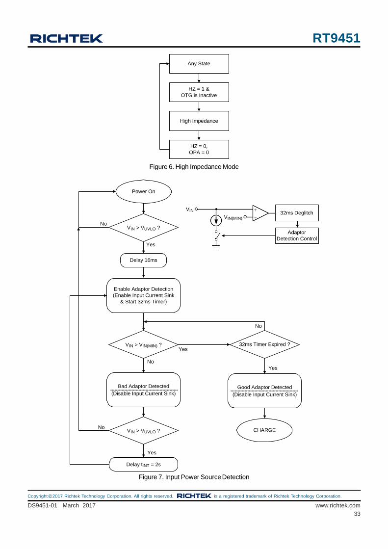
Bad Adapter Detection (CHBADI)
A mechanism is used to justify the power source capability
when power on at the VIN pin. When VIN rises above
VIN(MIN), a sink current of 30mA (typ.) is connected to VIN
pin to detection adaptor status. After the detection period
(30ms typ.), the sink current is removed. At the same
time, if VIN is still above VIN(MIN), the detection passes
and enters charge mode. If VIN is below VIN(MIN), the bad
adapter condition occurs. The RT9451 stops working, sets
CHBADI and repeats detection flow every 2 second (typ.).
Sleep Mode (VIN - VBATS < VSLP, CHRVPI)
The RT9451 enters sleep mode if the voltage drop between
the VIN and BATS pins falls below VSLP. In sleep mode,
the reverse blocking switch and PWM are all turned off.
This function prevents battery drain during poor or no input
power source.
Input Over-Voltage Protection (VINOVPI)
When VIN voltage raises above the input over-voltage
threshold (VOVP_IN), the RT9451 stops charging and then
sets fault status bits and sends out fault pulse via the
STAT pin. The condition is released when VIN falls below
VOVP_IN VOVP_IN. The RT9451 then resumes charging
operation.
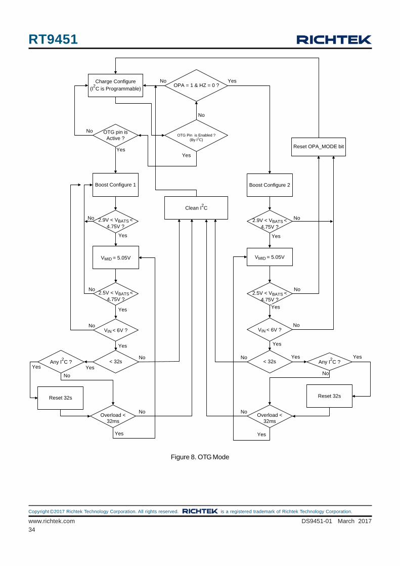
Boost Mode Operation (OTG)
Trigger and Operation
The RT9451 features USB OTG support. There are two
trigger method : One is to set CH_EN [1:0] = “01” (for
I2C control), the other is to set OTG_EN, OTG_PL and
OTG pin (for GPIO control). Notice that when using OTG
pin to trigger boost mode, it needs an edge trigger and
then keep it to the level defined by OTG_PL. When OTG
function is enabled, the synchronous Boost control loop
takes over the power MOSFETs and reverses the power
flow from the battery to the VIN pin. In normal boost mode,
the MID pin is regulated to the voltage level determined
by VOREG [5:0] whose range is from 4.75 and provides
up to 1.6A current to support other USB OTG devices
connected to the USB connector.
Safety Timer in Boost Mode (BST32SI)
Initially, the RT9451 starts a 32-second timer that can be
reset by any write or read action performed by the host
through the I2C interface. Once 32-second timer is expired,
the RT9451 enters to high impedance mode, the I2C
registers are all reset to default value and BST32S bit is
set to “1” to prevent the charger against uncontrolled
discharging when the dead lock of the host occurs.
During normal discharging process, the host needs to
reset 32-second timer periodically.
Output Over-Voltage Protection (VIN pin,
BSTVINOVI)
In boost mode, the output over-voltage protection is
triggered when the VIN voltage is above the output OVP
Page 31
RT9451
31
DS9451-01 March 2017 www.richtek.com
©Copyright 2017 Richtek Technology Corporation. All rights reserved. is a registered trademark of Richtek Technology Corporation.
threshold (6V typ.). When OVP occurs, the RT9451 stop
switching then enters high impedance mode.
Output Overload Protection (BSTOL)
The RT9451 provides an overload protection to prevent
the device and battery from damage when VIN is in
overload. Once the inductor current reaches cycle-by-cycle
current limit, the reverse blocking switch operates in linear
region to limit the output current while the MID voltage
remains in voltage regulation. If the overload condition lasts
for more than 30ms, the RT9451 determines the overload
fault condition and resets registers to the default settings.
Status Output (STAT pin)
The STAT pin is used to indicate operating conditions of
the RT9451 and is enabled by writing “00” to the
EN_STAT [1:0] in the register of address 0x00. When
charging is in progress, the STAT pin is pulled low. In
other conditions, the STAT pin acts as a high impedance
output. The STAT pin can also be always pulled low or
high impedance by writing “01” and “10” respectively.
Battery Protection
Battery Over-Voltage Protection in Charge Mode
(CHBATOVI)
The RT9451 monitors BATS voltage for output over-voltage
protection. In charge mode, if the BATS voltage rises above
VOVP_BAT x VOREG, for example, when the battery is
suddenly removed, the RT9451 stops charging and then
sets fault status bits and pull low INT pin. The condition is
released when BATS falls below (VOVP_BAT − ΔVOVP_BAT) x
VOVP_BAT. The RT9451 then resumes charging process
with default settings and the fault is cleared.
Battery Over/Under-Voltage Protection in Boost
Mode (BSTBATOVI, BSTLOWVI)
In boost mode, if the BATS voltage rises above the BATS
maximum input voltage (4.75V typ.) or below BATS
minimum input voltage (2.5V typ. for operating, 3V typ.
for start), battery over/under-voltage protection is triggered.
The RT9451 stops switching, and then enters high
impedance mode.
Thermal Considerations
For continuous operation, do not exceed absolute
maximum junction temperature. The maximum power
dissipation depends on the thermal resistance of the IC
package, PCB layout, rate of surrounding airflow, and
difference between junction and ambient temperature. The
maximum power dissipation can be calculated by the
following formula :
PD(MAX) = (TJ(MAX) − TA) / θJA
where TJ(MAX) is the maximum junction temperature, TA is
the ambient temperature, and θJA is the junction to ambient
thermal resistance.
For recommended operating condition specifications, the
maximum junction temperature is 125°C. The junction to
ambient thermal resistance, θJA, is layout dependent. For
WQFN-32L 4x4 package, the thermal resistance, θJA, is
27.8°C/W on a standard JEDEC 51-7 four-layer thermal
test board. The maximum power dissipation at TA = 25°Ccan be calculated by the following formula :
PD(MAX) = (125°C − 25°C) / (27.8°C/W) = 3.59W for
WQFN-32L 4x4 package
The maximum power dissipation depends on the operating
ambient temperature for fixed TJ(MAX) and thermal
resistance, θJA. The derating curve in Figure 2 allows the
designer to see the effect of rising ambient temperature
on the maximum power dissipation.
Figure 2. Derating Curve of Maximum Power Dissipation
0.0
0.5
1.0
1.5
2.0
2.5
3.0
3.5
4.0
0 25 50 75 100 125
Ambient Temperature (°C)
Ma
xim
um
Po
we
r D
issi
pa
tion
(W
) 1 Four-Layer PCB
Page 32
RT9451
32
DS9451-01 March 2017www.richtek.com
©Copyright 2017 Richtek Technology Corporation. All rights reserved. is a registered trademark of Richtek Technology Corporation.
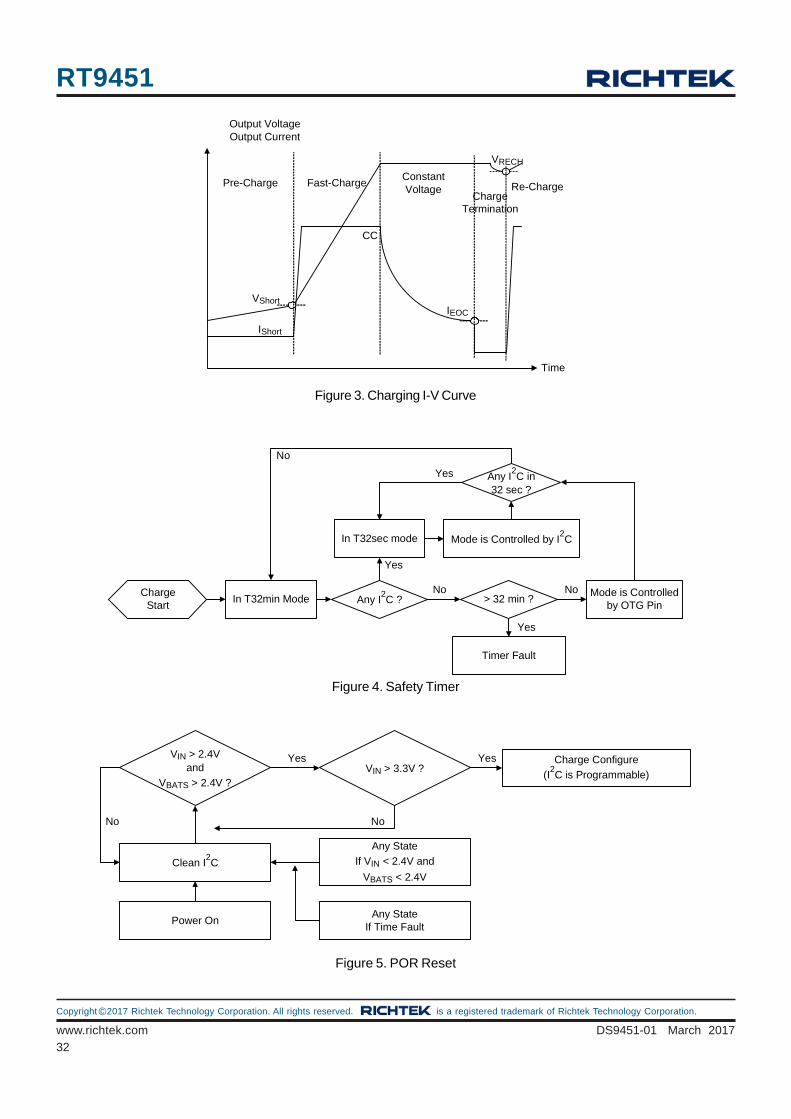
Figure 3. Charging I-V Curve
Figure 4. Safety Timer
Charge Start
In T32min Mode Any I2C ?
In T32sec mode
> 32 min ?
Timer Fault
Mode is Controlled by OTG Pin
Mode is Controlled by I2C
Any I2C in
32 sec ?
No
Yes
Yes
No No
Yes
Figure 5. POR Reset
Time
Output VoltageOutput Current
VShort
Pre-Charge
CC
VRECH
IShort
IEOC
Fast-ChargeConstant Voltage
Charge Termination
Re-Charge
VIN > 2.4Vand
VBATS > 2.4V ?
Charge Configure
(I2C is Programmable)
VIN > 3.3V ?
Power On
Clean I2C
Any State
If VIN < 2.4V and
VBATS < 2.4V
Any StateIf Time Fault
No
Yes Yes
No
Page 33
RT9451
33
DS9451-01 March 2017 www.richtek.com
©Copyright 2017 Richtek Technology Corporation. All rights reserved. is a registered trademark of Richtek Technology Corporation.
Figure 6. High Impedance Mode
Delay 16ms
Enable Adaptor Detection(Enable Input Current Sink
& Start 32ms Timer)
VIN > VIN(MIN) ?
Bad Adaptor Detected(Disable Input Current Sink)
Delay tINT = 2s
32ms Timer Expired ?
Good Adaptor Detected(Disable Input Current Sink)
Power On
CHARGE
VIN > VUVLO ?
VIN > VUVLO ?
Yes
Yes
Yes
Yes
No
No
No
No
VIN(MIN)
Adaptor Detection Control
32ms DeglitchVIN +
-
HZ = 1 & OTG is Inactive
High Impedance
HZ = 0, OPA = 0
Any State
Figure 7. Input Power Source Detection
Page 34
RT9451
34
DS9451-01 March 2017www.richtek.com
©Copyright 2017 Richtek Technology Corporation. All rights reserved. is a registered trademark of Richtek Technology Corporation.
2.9V < VBATS < 4.75V ?
Reset OPA_MODE bit
Boost Configure 2
VMID = 5.05V
Yes
2.5V < VBATS < 4.75V ?
Yes
VIN < 6V ?No
OTG pin is Active ?
Yes
Boost Configure 1
No
Charge Configure
(I2C is Programmable)
No
OPA = 1 & HZ = 0 ?
OTG Pin is Enabled ?(By I2C)
No
Yes
2.9V < VBATS < 4.75V ?
VMID = 5.05V
Yes
2.5V < VBATS < 4.75V ?
Yes
VIN < 6V ?
No
No
Overload < 32ms
Yes
Yes
Yes
Yes
No
Overload < 32ms
Any I2C ? < 32s
Yes
Reset 32s
Yes
No
< 32sYes
Any I2C ?
Reset 32s
Yes
No
Clean I2C
No
No
No No
No
No
Yes
Figure 8. OTG Mode
Page 35
RT9451
35
DS9451-01 March 2017 www.richtek.com
©Copyright 2017 Richtek Technology Corporation. All rights reserved. is a registered trademark of Richtek Technology Corporation.
Figure 9. Operation Flow Chart
Any State
OTG_EN = 1?
OTG Pin from High to Low @ OTG_PL = 0? or
OTG Pin from Low to High @ OTG_PL = 1?
OTG Mode
OTG Pin=High @ OTG_PL = 0? orOTG Pin=Low @ OTG_PL = 1?
VIN > VPOR_IN?
Power On
Load I2C with Default
Settings
VBATS > VSHORT? Charge with ISHORT
Fast-Charge with Low-CHRG
ICHRG < IEOC?
Termination is Enabled?
Keep in CV Mode
Charge Done------------------------
INT of Charge Termination
Re-Charge is Enabled?
VBATS < VRECH?
INT of Re-Charge
32 Min Timer Expired?
32 Min Timer Expired?
INT of TFault
Fault in Buck Mode(1) OVP(2) CHRVPI(3) TFault(4) CVOVP
OTG Mode
CH_EN[1:0] = [0,1]?
Fault?---------------------------------
VINOVP, VOCP, VBATUVP,
VBATOVP, T32s Fault
Set to Hi-Z Mode--------------------------CH_EN[1:0] = [0,0]
No
No
No No
No
No
No
No
No
No
Yes
No
Yes
Yes
Yes
Yes
Yes
Yes
Yes
Yes
Yes
Yes
Yes
Yes
No
Yes
No
Page 36
RT9451
36
DS9451-01 March 2017www.richtek.com
©Copyright 2017 Richtek Technology Corporation. All rights reserved. is a registered trademark of Richtek Technology Corporation.
Layout Considerations
Place the input and output capacitors as close to the input
and output pins as possible.
Keep the main power traces as wide and short as
possible.
The output inductor and bootstrap capacitor should be
placed close to the chip and LX pins.
To optimize current sense accuracy, connect the traces
to RSENSE with Kelvin sense connection.
Figure 10. PCB Layout Guide
VIN
VINVINVIN
PGND
PGNDPGNDPGND
SD
AS
TA
TO
TG
BA
TS
MID
LX
LX
LX
VIOINT
VDDPGND
SC
LM
ID
ISE
NL
LX
DP BOOT
ISE
NR
LX
LD
OP
GN
D
DM MID_LDO
33
24
23
22
21
1
2
3
4
10 11 12 13
31 30 29 28
20
19
5
6
9
32
14
27
187
15
26
16
25
178
GND
To System
To Battery
GND
GND
To optimize current and voltage sense accuracy, connect the traces to pins with Kelvin sense connection.
Keep the main power traces as wide and short as possible.
Keep the main power traces as wide and short as possible.
The output inductor and bootstrap capacitor should be placed close to the chip And LX pins.
Keep the main power traces as wide and short as possible.
Place the input and output capacitors as close to the input and output pins as possible.
Page 37
RT9451
37
DS9451-01 March 2017 www.richtek.com
Richtek Technology Corporation5F, No. 20, Taiyuen Street, Chupei City
Hsinchu, Taiwan, R.O.C.
Tel: (8863)5526789
Richtek products are sold by description only. Richtek reserves the right to change the circuitry and/or specifications without notice at any time. Customers should
obtain the latest relevant information and data sheets before placing orders and should verify that such information is current and complete. Richtek cannot
assume responsibility for use of any circuitry other than circuitry entirely embodied in a Richtek product. Information furnished by Richtek is believed to be
accurate and reliable. However, no responsibility is assumed by Richtek or its subsidiaries for its use; nor for any infringements of patents or other rights of third
parties which may result from its use. No license is granted by implication or otherwise under any patent or patent rights of Richtek or its subsidiaries.
Outline Dimension
Dimensions In Millimeters Dimensions In Inches Symbol
Min Max Min Max
A 0.700 0.800 0.028 0.031
A1 0.000 0.050 0.000 0.002
A3 0.175 0.250 0.007 0.010
b 0.150 0.250 0.006 0.010
D 3.900 4.100 0.154 0.161
D2 2.650 2.750 0.104 0.108
E 3.900 4.100 0.154 0.161
E2 2.650 2.750 0.104 0.108
e 0.400 0.016
L 0.300 0.400 0.012 0.016
W-Type 32L QFN 4x4 Package
Note : The configuration of the Pin #1 identifier is optional,
but must be located within the zone indicated.
DETAIL A
Pin #1 ID and Tie Bar Mark Options
11
2 2