22
Yifei Li, Zhen Zhang and Nathan M. Neihart Iowa State University MWSCAS 2014-College Station, TX. Switchless Matching Networks for Dual-Band Class-E Power Amplifiers

Yifei Li, Zhen Zhang and Nathan M. Neihart
Iowa State University
MWSCAS 2014-College Station, TX.
Switchless Matching Networks for
Dual-Band Class-E Power Amplifiers

Outline
Motivations
Dual-Band Matching Networks for Power Amplifiers
Proposed Dual-Band Matching Networks for Class E PA
Simulation Results
Conclusion
2/22

Motivations
Multi-band radio is a basic requirement for today’s
wireless devices
Non-contiguous Carrier Aggregation requires
concurrent operation
Simultaneous tasks
20 MHz
20 MHz
20 MHz
20 MHz
20 MHz Carrier #1
Carrier #2
Carrier #3
Carrier #5
Carrier #4
AggregatedMobile Data
Pipe
100 MHzCapacity
3/22

Primary
Antenna
Antenna
Switch
GSM Tx
GSM Tx
WCDMA Tx
WCDMA Tx
PA
PA
Motivation for Dual-Band/Multi-Band Power Amplifier
PA is a major part of
RF front end
Multi-band PA brings
Smaller area
Lower costIPhone 5 mother board
Typical PA module 4/22

Outline
Motivations
Dual-Band Output Matching Networks for Power Amplifiers Switch-Based
Transmission-Line Based
Lumped Element Based
Proposed Dual-Band Matching Networks for Class E PA
Simulation Results
Conclusion
5/22

Single and Dual-Band Output Matching Networks
Output matching networksconverts 50Ω antenna load to desired load impedance(ZLoad) seen by the transistor
Usually low impedance Single-band OMN:
conversion onlyachieved at one frequency
Dual-band OMN:conversion can beachieved at two frequencies
We care about: desired impedance loss
50Ω
ZLoad
50Ω
ZLoad
6/22

Switch-Based Output Matching Networks
Disadvantages
Extra cost of RF switches
Extra loss of RF switches
Does not support concurrent operation
Advantages
Simple design
Can be extended to multiple bands
50Ω
ZLoad
7/22Luca Larcher et al, Design, Automation & Test in Europe Conference & Exhibition, Apr. 2009, pp.364-368.

Transmission Line and Lumped Element Output
Matching Networks
Transmission line OMN
Disadvantages: Large area
Advantages: Low loss
Lump element OMN
Advantages: Small area.
Disadvantages: Circuit complexity an loss increase with number of
supported frequency bands (beyond 3 bands)
This particular lumped element OMN has no control on harmonics
50Ω
VDD
λ/4 @ 3f2
λ/4 @ 3f2
λ/4 @ 3f1
λ/2 @ 2f2λ/4 @ 2f1
ZLoad
50Ω
VDD
ZLoad
8/22Danish Kalim et al, IEEE International Microwave Symposium Digest(MTT), Jun. 2011, PP.1-4.Koji Uchida et al, IEEE Asian-Pacific Microwave Conference Proceedings, Dec.2005.
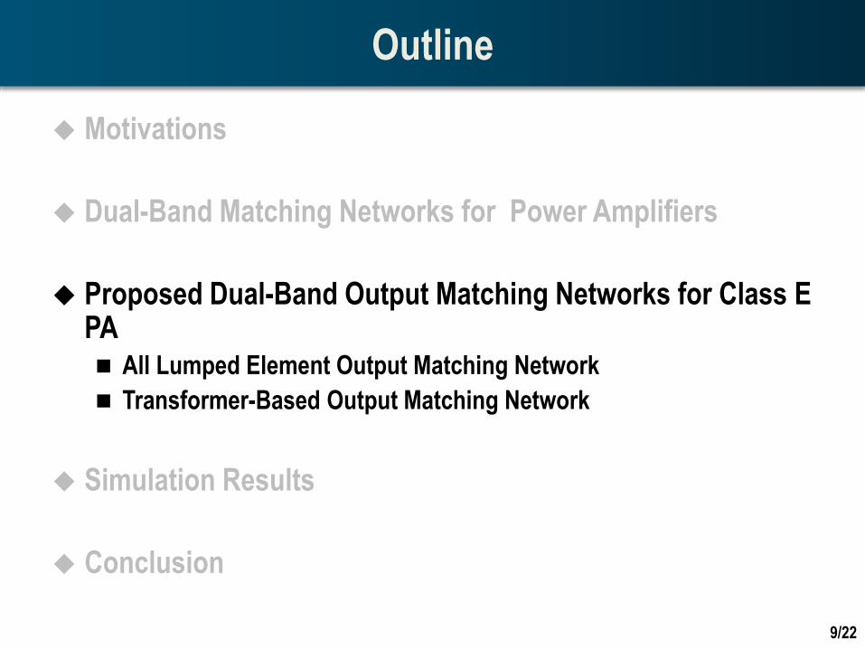
Outline
Motivations
Dual-Band Matching Networks for Power Amplifiers
Proposed Dual-Band Output Matching Networks for Class E PA All Lumped Element Output Matching Network
Transformer-Based Output Matching Network
Simulation Results
Conclusion
9/22

Conventional Single-Band Output Matching Network for
Class E PA
Desired ZLoad=7+j8 Ω at the design frequency, and high
absolute impedance at harmonics
Part A realizes real-to-real impedance conversion,
providing real part of desired impedance, RL, at design
frequency
Part B provides XL at the design frequency and high
impedance at harmonics
10/22
50Ω AB
RLZLoad=jXL+RL
Lx CoLo Cs
Lp

Proposed Dual-Band Output Matching Networks for
Class E PA
Desired impedance: 7+j8 Ω @ 800MHz and 1900MHz
Proposed all-lumped element output matching network
Proposed transformer-based output matching network
50Ω CPLP
CSLSL1
L2
CO
C2
k
Zeff A
RL
B
ZLoad=jXL+RL 11/22
50Ω
CPLP
CSLS
L1 L2CO
C2 AB
RLZLoad=jXL+RL

All-Lumped Element Dual-Band OMN
First consider the real-to-real
impedance conversion
Part A converts 50Ω to 7Ω at bothfrequencies
CsL, LpL form equivalent low-band
L match
CsH, LpH form equivalent high-band
L match
Component values in equivalent
single-band MNs can be
calculated at each
frequency CpH
LsH
50Ω
CsL
LpL50Ω
Low Band High Band
50Ω
CPLP
CSLS
RL
RL,Low RL,High
12/22
50Ω
CPLP
CSLS
L1 L2CO
C2 AB
RLZLoad=jXL+RL

50Ω
CPLP
CSLS
L1 L2CO
C2 AB
RLZLoad=jXL+RL
All-Lumped Element Dual-Band OMN
Now consider the positive reactance Part B provides +j8 Ω at both frequencies and high impedance at
their harmonics
Green box acts as a variable inductor
How to determine CO
Trade off between harmonic impedance (loss in power transistor) and loss in the matching network
LxH CoLoH LxL CoLoL
High band Low band
13/22

Transformer-Based Dual-Band OMN
Part B provides +j8 Ω at both frequencies, and high impedance at their harmonics
Green box acts as a variable inductor Red part of the expression is what we used
The rest is parasitic resistance
where
𝜔𝑜 = 1/ 𝐿2𝐶2,
𝑄 =𝜔𝑜𝐿2𝑅2
,
𝑎(𝐿,𝐻) = 𝜔(𝐿,𝐻)/𝜔𝑜
LxH CoLoH LxL CoLoL
High band Low band
𝑍𝑒𝑓𝑓 = 𝜔𝐿1
𝑘2𝑎
𝑄
1
𝑎−𝑎
2+
1
𝑄2
+ 𝑗𝜔𝐿1 1 +𝑘2 1−𝑎2
1
𝑎−𝑎
2+
1
𝑄2
14/22
50Ω CPLP
CSLSL1
L2
C2
k
Zeff A
RL
B
ZLoad=jXL+RL
CO

Loss Optimization of Transformer-Based OMN
Sweep 𝜔𝑜, for each 𝜔𝑜, the values
of 𝐿1and 𝑘 can be determined.
Loss model
Total loss in terms of parasitic resistance is expressed as
Parasitic resistance from the primary winding
Reflected parasitic resistance from the secondary winding
𝐿1 1 +𝑘2 1−𝑎2
1
𝑎−𝑎
2+
1
𝑄2
= 𝜔𝐿(𝐿𝑋𝐿+𝐿𝑂𝐿)
𝐿1 1 +𝑘2 1−𝑎2
1
𝑎−𝑎
2+
1
𝑄2
= 𝜔𝐻(𝐿𝑋𝐻+𝐿𝑂𝐻)
𝑃𝑎𝑟𝑎𝑠𝑖𝑡𝑖𝑐 𝑅𝑒𝑠 Ω = 𝜔𝐿1
𝑘2𝑎𝑄
1𝑎 − 𝑎
2
+1𝑄2
+𝜔𝐿1𝑄𝑥
𝑄𝑥 is the quality factor of 𝐿1 at each frequency
LxH CoLoH LxL CoLoL
High bandLow band
15/22
50Ω CPLP
CSLSL1
L2
C2
k
Zeff A
RL
B
ZLoad=jXL+RL
CO

Loss Optimization of Transformer-Based OMN
Trade off between OMN loss and transistor loss
Higher harmonic impedance -> low loss in transistor
To increase the impedance at the 2nd harmonic of low band, 𝝎𝟎 should be
closer to 𝟐𝒇𝑳.
𝜔𝑜is set at 2π*1.25G rad/s
Higher loss in high band OMN
Higher loss in low band power transistor
16/22Resonant frequency [GHz]
Para
siti
c R
esH [Ω
]
Resonant frequency [GHz]
Par
asit
ic R
esL [Ω
]
Outline
Motivations
Dual-Band Matching Networks for Power Amplifiers
Proposed Dual-Band Matching Networks for Class E PA
Simulation Results
Conclusion
17/22

Simulation Results
Simulation environment
HBT power transistor with 3.5V power supply
TDK MHG0603 (mm) inductors
Murata GJM 0603 (mm) capacitor
Low DC resistance (mΩ) 1μH choke Inductor
Operation frequencies: 800MHz and 1900MHz
Substrate: 2-layer PCB with a thickness of 864μm, average dielectric constant of 3.57, metal thickness of 18μm, average loss tangent of 0.0036
Component values
L1 (nH) L2 (nH) C2 (pF) C3 (pF) k
All-lumped 7 3.7 3.5 3.6 –
Transformer-based
8.1 4 4.1 4.5 0.64
LS (nH) CS (pF) LP (nH) CP (pF)
2.5 6.6 2.3 7.2
18/22
OMN
50Ω
VDD
Choke Ind

Simulation Results
All-lumped output matching network
At 800MHz, η=71%@30.2dBm
At 1.9GHz, η=68%@29dBm
Transformer-based output matching network
At 800MHz, η=75%@30.1dBm
At 1.9GHz, η=67%@27.4dBm
19/22All-lumped element Transformer based

Simulated Performance Comparison
RefFrequency Band
(GHz)
Simulated output Power*
(watt/V2)
Simulated Efficiency(%)
Load Type
[2] 0.9/1.8 0.011 η=44/40Switch-
based/off chip
[3]1.9/2.3/2.6/3.5
0.02η=64/62/59/58
On-chip
[4] 1.81/2.65 0.0075η=73.6/
70.1TLs
[6]** 0.8/1.5 0.05/0.026PAE=51.6/
51.9Lumped/Off chip
This work all-lump load network
0.8/1.9 0.067/0.038 η=75/67 Lumped/Off chip
This work transformer
based 0.8/1.9 0.038 η=71/68 Lumped/
Off chip
* Output power normalized to V2DD
** Measured Result
20/22
Luca Larcher et al, Design, Automation & Test in Europe Conference & Exhibition, Apr. 2009, pp.364-368.Ki Young Kim et al, IEEE Microwave and Wireless Components Letters, vol.21, no.7, July.2011.Danish Kalim et al, IEEE International Microwave Symposium Digest (MTT), Jun. 2011, pp.1-4.Koji Uchida et al, IEEE Asian-Pacific Microwave Conference Proceedings, Dec.2005.
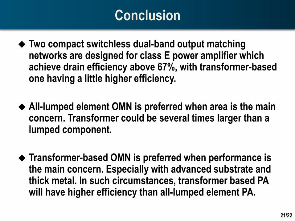
Conclusion
Two compact switchless dual-band output matching networks are designed for class E power amplifier which achieve drain efficiency above 67%, with transformer-based one having a little higher efficiency.
All-lumped element OMN is preferred when area is the main concern. Transformer could be several times larger than a lumped component.
Transformer-based OMN is preferred when performance is the main concern. Especially with advanced substrate and thick metal. In such circumstances, transformer based PA will have higher efficiency than all-lumped element PA.
21/22

Questions
22/22


