25
SYEN 3330 Digital Systems Jung H. Kim Chapter 3 1 SYEN 3330 Digital Systems Chapter 3
| Date post: | 01-Jan-2016 |
| Category: |
Documents |
| Upload: | zoe-singleton |
| View: | 53 times |
| Download: | 0 times |

SYEN 3330 Digital Systems Jung H. Kim Chapter 3 1
SYEN 3330Digital Systems
Chapter 3
SYEN 3330 Digital Systems Chapter 3 Page 2
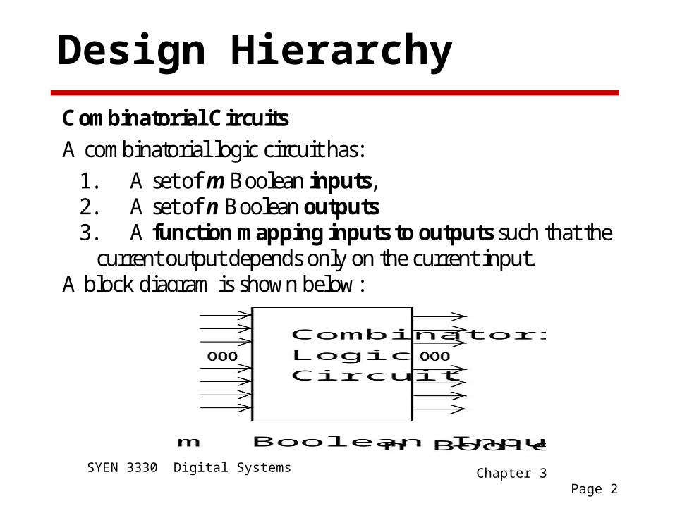
Design Hierarchy
Combinatorial Circuits
A combinatorial logic circuit has:
1. A set of m Boolean inputs,2. A set of n Boolean outputs3. A function mapping inputs to outputs such that the
current output depends only on the current input.A block diagram is shown below:
SYEN 3330 Digital Systems Chapter 3 Page 3
Hierarchical Design
The function mapping inputs to outputs may be very complex.
To control complexity, we decompose the function into smaller pieces called blocks.
The blocks are subdivided into finer blocks.
The "leaves” in the hierarchy are called primitive blocks.
Example: 16 input parity tree
Top Level: 16 inputs, one output
2nd Level: 5- four bit parity trees in two levels.
3rd Level: 3, two-bit exclusive-OR functions.
Primitive level: 4 two-input NANDs
The design requires 5 X 3 X 4 = 64 two-input NAND gates.
SYEN 3330 Digital Systems Chapter 3 Page 4
Reusable Functions and Design
Wherever possible, we try to decompose a complex design into common, reusable function blocks.
These blocks are tested and well documented.
Computer-aided design (CAD) tools might include them in libraries.
Computer-aided manufacturing (CAM) tools might know how to manufacture and test them.
Other tools: Schematic Capture
Logic Simulators
Timing Verifiers
Hardware Description Languages (HDL)
SYEN 3330 Digital Systems Chapter 3 Page 5
Top-Down verses Bottom Up
A Top-Down design proceeds from an abstract, high level specification to a more and more detailed design by decomposition and successive refinement.
A Bottom-Up design starts with detailed primitive elements and combines them into larger and larger and more complex functions.
Designs usually proceed from both directions simultaneously.
Top-Down design answers: What are we building?
Bottom-Up design answers: How do we build it?
Top-Down controls complexity while Bottom-Up "sweats" the details.
We will start first with ANALYSIS.
SYEN 3330 Digital Systems Chapter 3 Page 6
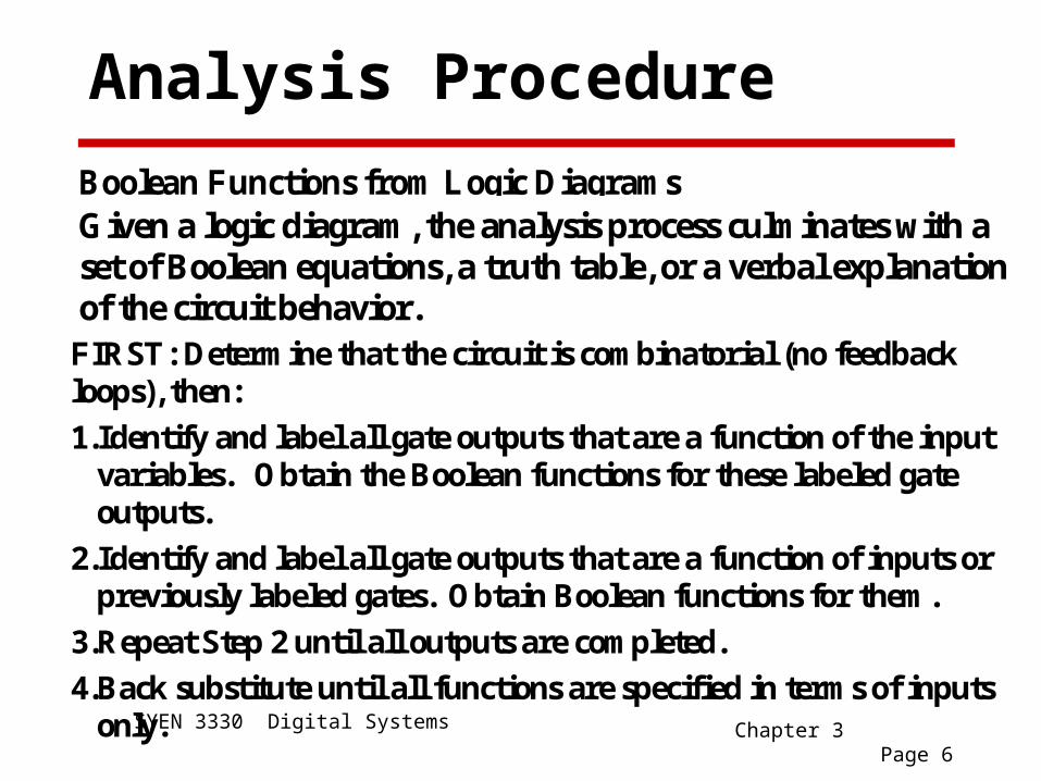
Analysis Procedure
Given a logic diagram, the analysis process culminates with a set of Boolean equations, a truth table, or a verbal explanation of the circuit behavior.
Boolean Functions from Logic Diagrams
FIRST: Determine that the circuit is combinatorial (no feedback loops), then:
1. Identify and label all gate outputs that are a function of the input variables. Obtain the Boolean functions for these labeled gate outputs.
2. Identify and label all gate outputs that are a function of inputs or previously labeled gates. Obtain Boolean functions for them.
3. Repeat Step 2 until all outputs are completed.
4. Back substitute until all functions are specified in terms of inputs only.
SYEN 3330 Digital Systems Chapter 3 Page 7
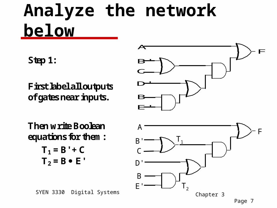
Analyze the network below
FA
B'C
D'
B
E'
FA
B'C
D'
B
E'
T1
T2
T3
T4
Step 1:
First label all outputs of gates near inputs.
Then write Boolean equations for them:
T1 = B' + C T2 = B E'
FA
B'C
D'
BE'
T1
T2
SYEN 3330 Digital Systems Chapter 3 Page 8
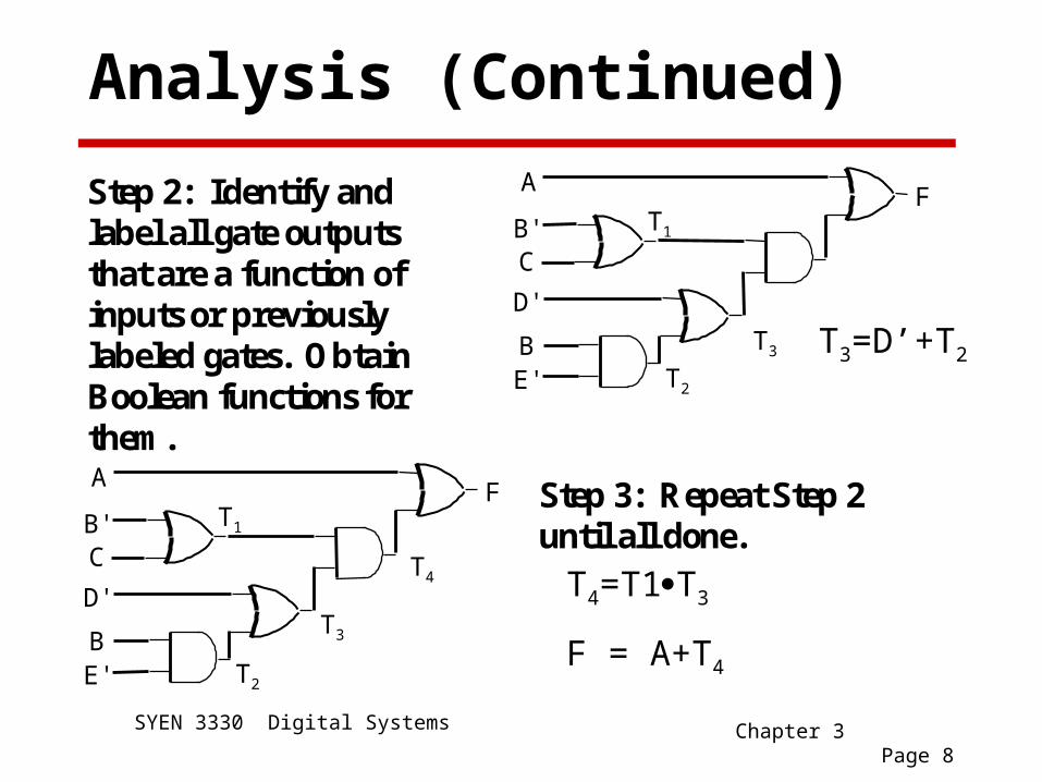
Analysis (Continued)
Step 2: Identify and label all gate outputs that are a function of inputs or previously labeled gates. Obtain Boolean functions for them.
Step 3: Repeat Step 2 until all done.
FA
B'C
D'
BE'
T1
T2
T3
FA
B'C
D'
BE'
T1
T2
T4
T3
T3=D’+T2
T4=T1T3
F = A+T4
SYEN 3330 Digital Systems Chapter 3 Page 9
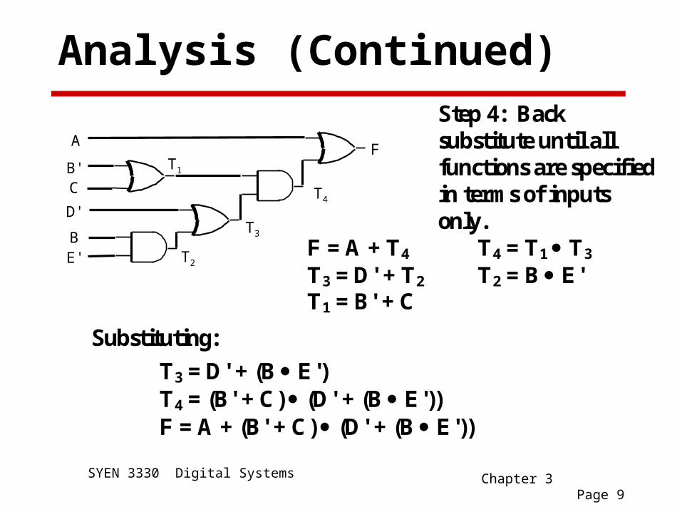
Analysis (Continued)Step 4: Back substitute until all functions are specified in terms of inputs only.
F = A + T4 T4 = T1 T3 T3 = D' + T2 T2 = B E' T1 = B' + C
Substituting:
T3 = D' + (B E') T4 = (B' + C) (D' + (B E')) F = A + (B' + C) (D' + (B E'))
FA
B'C
D'
BE'
T1
T2
T4
T3
SYEN 3330 Digital Systems Chapter 3 Page 10
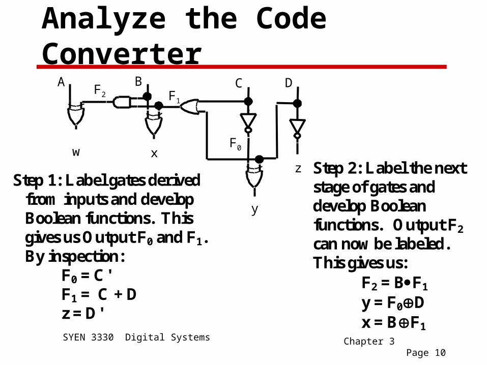
Analyze the Code Converter
Step 1: Label gates derived from inputs and develop Boolean functions. This gives us Output F0 and F1. By inspection: F0 = C' F1 = C + D z = D'
Step 2: Label the next stage of gates and develop Boolean functions. Output F2 can now be labeled. This gives us: F2 = BF1 y = F0D x = BF1
w x
y
z
A B C DF1
F2
F0
SYEN 3330 Digital Systems Chapter 3 Page 11
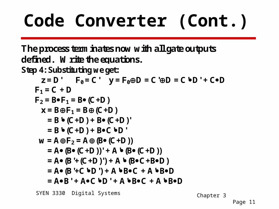
Code Converter (Cont.)
The process terminates now with all gate outputs defined. Write the equations.
Step 4: Substituting we get: z = D' F0 = C' y = F0D = C'D = C'D' + CD F1 = C + D F2 = BF1 = B(C+D) x = BF1 = B(C+D) = B'(C+D) + B(C+D)' = B'(C+D) + BC'D' w = AF2 = A(B(C+D)) = A(B(C+D))' + A'(B(C+D)) = A(B'+(C+D)') + A'(BC+BD) = A(B'+C'D') + A'BC + A'BD = AB' + AC'D' + A'BC + A'BD
SYEN 3330 Digital Systems Chapter 3 Page 12
Truth Tables from Diagrams
1. Determine the number of input variables, n. There will be 2n input vectors from zero to 2n -1. Enter them in the table.
2. Label the outputs of selected gates with symbols and enter a column for each one in the table.
3. Obtain the truth table for the outputs of those gates that are a function of only input variables.
4. Proceed to fill in the outputs of all gates that are derived from inputs and previously calculated terms.
Example: Find the function table for the code converter.
We will use the same markings as before and define a truth table on those values.

SYEN 3330 Digital Systems Chapter 3 Page 13
Code Converter Truth Table
Four inputs give 16 input vectors. Start with F0, F1 and z:
ABCD F0 F1 F2 w x y z 0000 1 1 0001 1 0 0010 0 1 0011 0 0 0100 1 1 0101 1 0 0110 0 1 0111 0 0 1000 1 1 1001 1 0 1010 0 1 1011 0 0 1100 1 1 1101 1 0 1110 0 1 1111 0 0

SYEN 3330 Digital Systems Chapter 3 Page 14
Truth Table Fill-In
Now we can calculate x, y, and F2:
ABCD F0 F1 F2 w x y z 0000 1 0 0 0 1 1 0001 1 1 1 1 0 0 0010 0 1 1 1 0 1 0011 0 1 1 1 1 0 0100 1 0 1 1 1 1 0101 1 1 1 0 0 0 0110 0 1 1 0 0 1 0111 0 1 1 0 1 0 1000 1 0 0 0 1 1 1001 1 1 1 1 0 0 1010 0 1 1 1 0 1 1011 0 1 1 1 1 0 1100 1 0 1 1 1 1 1101 1 1 1 0 0 0 1110 0 1 1 0 0 1 1111 0 1 1 0 1 0

SYEN 3330 Digital Systems Chapter 3 Page 15
Finish Up Entries
Finally we can add w to complete the table:
ABCD F0 F1 F2 w x y z 0000 1 0 0 0 0 1 1 0001 1 1 1 0 1 0 0 0010 0 1 1 0 1 0 1 0011 0 1 1 0 1 1 0 0100 1 0 1 0 1 1 1 0101 1 1 1 1 0 0 0 0110 0 1 1 1 0 0 1 0111 0 1 1 1 0 1 0 1000 1 0 0 1 0 1 1 1001 1 1 1 1 1 0 0 1010 0 1 1 1 1 0 1 1011 0 1 1 1 1 1 0 1100 1 0 1 1 1 1 1 1101 1 1 1 0 0 0 0 1110 0 1 1 0 0 0 1 1111 0 1 1 0 0 1 0
SYEN 3330 Digital Systems Chapter 3 Page 16
What Does the Circuit Do?
By inspection, we notice that the output variable vector (w,x,y,z) is just the input variable vector (A,B,C,D) plus three.
The function(s) F(A,B,C,D) = (w,x,y,z) are: "ADD THREE TO THE INPUT VECTOR"
Function F1 has the meaning: "ADD ONE TO THE UPPER TWO BITS"
Similarly, function F2 has the meaning: "ADD ONE TO THE UPPER BIT"
Generally, it is not this obvious to figure out what the functions mean!

SYEN 3330 Digital Systems Chapter 3 Page 17
Final Note (and warning)The use of "Don't Cares" in the original specification can
cloud the analysis.
Note that the functions for the "w" bit differ from the implementation in Ex. 3-2 of the book. The book made an assignment to the "Don't Cares" to simplify the logic. The example here did not.
This can be seen by inspecting the two Karnaugh Maps for the function w:
Ex. 3-2 in book Example here(used dc's) (no dc's)
SYEN 3330 Digital Systems Chapter 3 Page 18
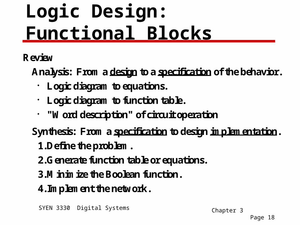
Logic Design: Functional Blocks
Review
Analysis: From a design to a specification of the behavior. Logic diagram to equations. Logic diagram to function table. "Word description" of circuit operation
Synthesis: From a specification to design implementation.
1. Define the problem.
2. Generate function table or equations.
3. Minimize the Boolean function.
4. Implement the network.

SYEN 3330 Digital Systems Chapter 3 Page 19
Review Combinatorial Logic
A combinatorial logic circuit has: 1. A set of m Boolean inputs, 2. A set of n Boolean outputs 3. A function mapping inputs to outputs.
We think of the function as n separate Boolean functions of m inputs.
Procedure: Treat each output as a separate function. Minimize the equations for each function. Implement each function independently.
Sometimes an implementation can share product or sum logic terms to arrive at a lower literal cost solution.

SYEN 3330 Digital Systems Chapter 3 Page 20
Design Procedure
First, start with the specification of the circuit to be designed.
Note: this can sometimes require a lot of work to complete the specification process, especially if it is poorly specified initially.
Second, follow these steps:
1. Identify the inputs and outputs.
2. Derive truth table.
3. Obtain simplified Boolean equations.
4. Draw the logic diagram
5. Check your work to verify correctness.
We will study the design of a code converter to see these steps.

SYEN 3330 Digital Systems Chapter 3 Page 21
Code Converter DesignA code converter transforms one internal representation of
data to another.
We will start with a table of the desired conversion and minimize the resulting Multiple Output Boolean function.
Sometimes terms can be shared to minimize the implementation cost.
The Problem:
Design a BCD to Excess-3 code converter.
Specification:
BCD code -- 4-bit patterns "0000" to "1001" for digits 0 to 9 base 10.
Excess-3 -- BCD code plus binary "0011" for digits 0 to 9 base 10.

SYEN 3330 Digital Systems Chapter 3 Page 22
Example: BCD to Excess 3
Function table: Input BCD A B C D
Output Excess-3 w x y z
0 0 0 0 0 0 1 1 0 0 0 1 0 1 0 0 0 0 1 0 0 1 0 1 0 0 1 1 0 1 1 0 0 1 0 0 0 1 1 1 0 1 0 1 1 0 0 0 0 1 1 0 1 0 0 1 0 1 1 1 1 0 1 0 1 0 0 0 1 0 1 1 1 0 0 1 1 0 1 1
Note:
All BCD codes greater than "9" can be assigned "Don't Cares" in the K-Map. Such BCD codes are never possible.

SYEN 3330 Digital Systems Chapter 3 Page 23
Example (Cont.): BCD to Excess 3
Minimize each equation
Minimized Equations:
z = D '
y=CD + C 'D ' (exnor)
x=B 'C + B 'D + BC 'D '
w = A + BC + BD

SYEN 3330 Digital Systems Chapter 3 Page 24
BCD to Excess 3 Implementation
First we will manipulate the equations to expose some shared terms:
z = D'
y = CD + C'D' (This is an EXNOR)
x = B'C + B'D + BC'D' = B'(C + D) + BC'D'
w = A + BC + BD = A + B(C + D)
The term (C + D) can be used more than once to simplify the implementation.
See Fig. 3-10 in Mano and Kime for the implementation.

SYEN 3330 Digital Systems Chapter 3 Page 25
BCD to Excess 3
Another Approach: Note that Excess-3 is defined as "BCD plus 3". Thus we can use the simple algorithm shown below to compute Excess-3 from BCD.
One implementation is:
CoCi
x y
S
HACo
x y
S
HACoCi
x y
S
FACo
x y
S
HA
A B C D"1""1"
w x y z
A B C D
+ 0 0 1 1
w x y z
Here HA is a Half-Adder and FA is a Full-Adder (We will discuss these later in the chapter).


