20
SYEN 3330 Digital Systems Jung H. Kim Chapter 2-7 1 SYEN 3330 Digital Systems Chapter 2 Part 7
| Date post: | 22-Dec-2015 |
| Category: |
Documents |
| View: | 227 times |
| Download: | 0 times |

SYEN 3330 Digital Systems Jung H. Kim Chapter 2-7 1
SYEN 3330 Digital Systems
Chapter 2 Part 7
SYEN 3330 Digital Systems Chapter 2-7 Page 2
NAND and NOR Implementation
We found that we could implement general Boolean equations with these three primitives:
1. AND
2. OR
3. NOT
In this section we will find that either of two gates, the NAND gate or the NOR gate can be used to implement arbitrary logic functions.
NOTE: The book uses the Positive Logic Convention (where all signals are active high) and uses a small circle to represent complementation.
SYEN 3330 Digital Systems Chapter 2-7 Page 3
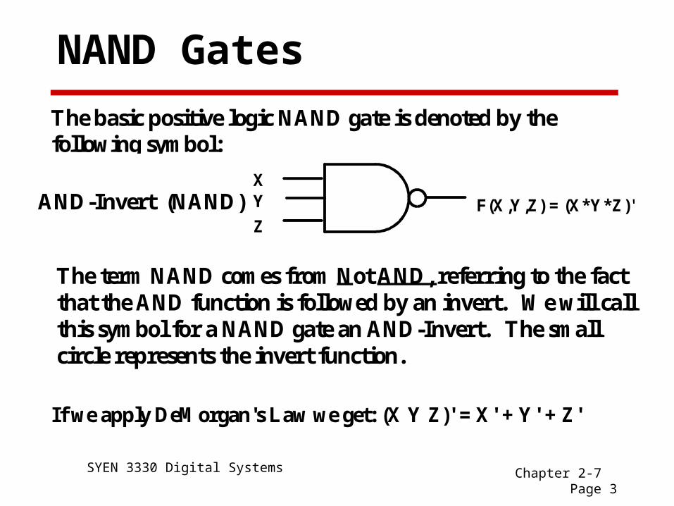
NAND Gates
The basic positive logic NAND gate is denoted by the following symbol:
XY
ZF(X,Y,Z) = (X*Y*Z)'AND-Invert (NAND)
The term NAND comes from Not AND, referring to the fact that the AND function is followed by an invert. We will call this symbol for a NAND gate an AND-Invert. The small circle represents the invert function.
If we apply DeMorgan's Law we get: (X Y Z)' = X' + Y' + Z'

SYEN 3330 Digital Systems Chapter 2-7 Page 4
NAND Gates (Cont.)
The application of DeMorgan's Law leads to the following symbol for a NAND Gate:
XY
ZF(X,Y,Z) = X'+Y'+Z'Invert-Or
We call this symbol the Invert-OR since all inputs are inverted, followed by the OR function. Note that both symbols are used to represent the NAND gate - it is sometimes more convenient (or logically descriptive) to use one form over the other.
A single NAND gate with one input is degenerate and becomes an inverter.

SYEN 3330 Digital Systems Chapter 2-7 Page 5
NAND ImplementationNAND gates can be used to implement a simplified Sum-of-Products form of a Boolean equation. To see this, let us construct a two level NAND-NAND gate function thus:
The first level uses two, 2-input NAND gates shown as the AND-Invert symbol. The second level uses one, 2-input NAND gate shown as the Invert-OR symbol. Using the NAND relationship, we have:
A
B
C
DG(A,B,C,D) = A*B + C*D
G(A,B,C,D)
G(A,B,C,D) = ((AB)'(CD)')' = ((AB)')'+((CD)')' = (AB) + (CD)
SYEN 3330 Digital Systems Chapter 2-7 Page 6
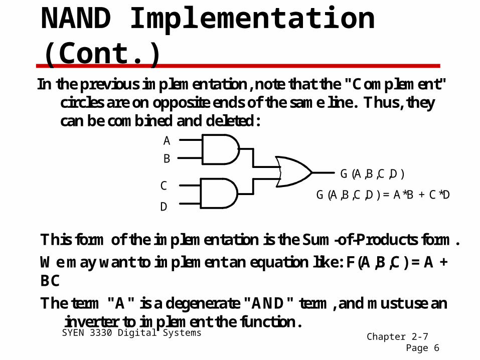
NAND Implementation (Cont.)
In the previous implementation, note that the "Complement" circles are on opposite ends of the same line. Thus, they can be combined and deleted:
A
B
C
DG(A,B,C,D) = A*B + C*D
G(A,B,C,D)
This form of the implementation is the Sum-of-Products form.
We may want to implement an equation like: F(A,B,C) = A + BC
The term "A" is a degenerate "AND" term, and must use an inverter to implement the function.
SYEN 3330 Digital Systems Chapter 2-7 Page 7
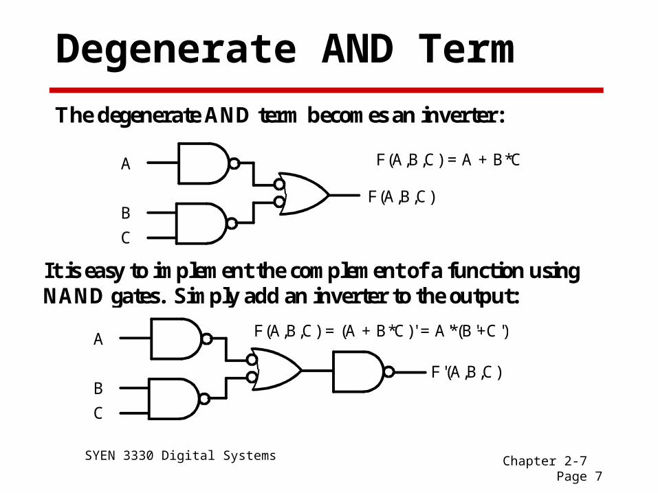
Degenerate AND Term
A
B
C
F(A,B,C) = A + B*C
F(A,B,C)
A
B
C
F(A,B,C) = (A + B*C)' = A'*(B'+C')
F'(A,B,C)
It is easy to implement the complement of a function using NAND gates. Simply add an inverter to the output:
The degenerate AND term becomes an inverter:
SYEN 3330 Digital Systems Chapter 2-7 Page 8
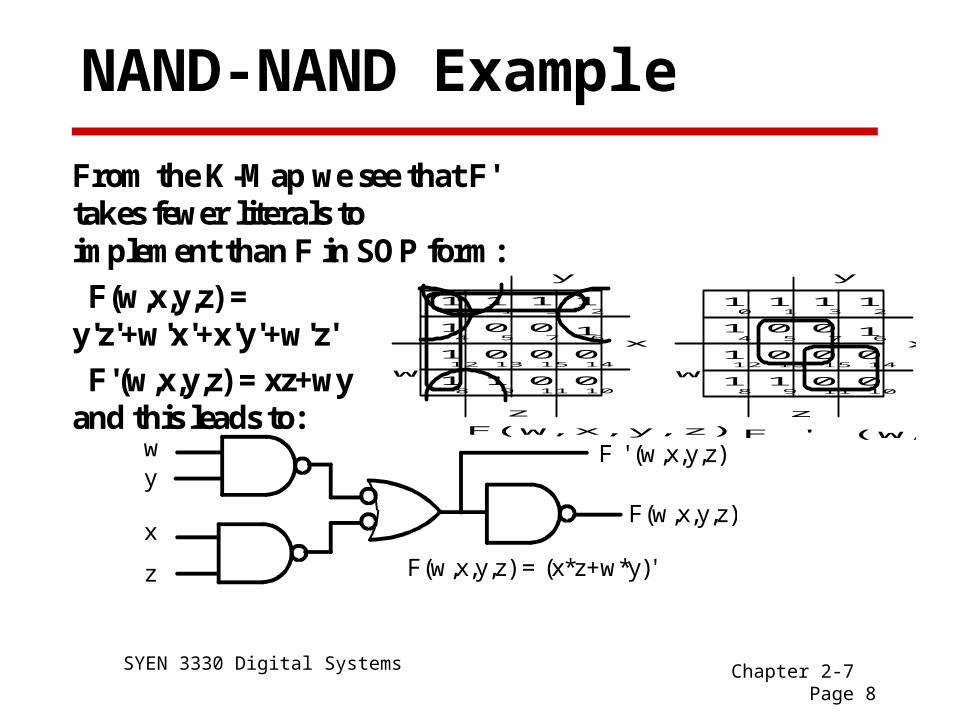
NAND-NAND Example
x
y
z
w
0 1 3 2
4 5 7 6
12 13 15 14
8 9 11 10
1 1 1 1
11
1
1 1
0 0
0 0 0
0 0
x
z
w
0 1 3 2
4 5 7 6
12 13 15 14
8 9 11 10
1 1 1 1
11
1
1 1
0 0
0 0 0
0 0
y
F(w,x,y,z) F ' (w,x,y,z)
From the K-Map we see that F' takes fewer literals to implement than F in SOP form:
F(w,x,y,z) = y'z'+w'x'+x'y'+w'z'
F'(w,x,y,z) = xz+wy and this leads to:
F(w,x,y,z) = (x*z+w*y)'
F(w,x,y,z)
wy
x
z
F ' (w,x,y,z)
SYEN 3330 Digital Systems Chapter 2-7 Page 9
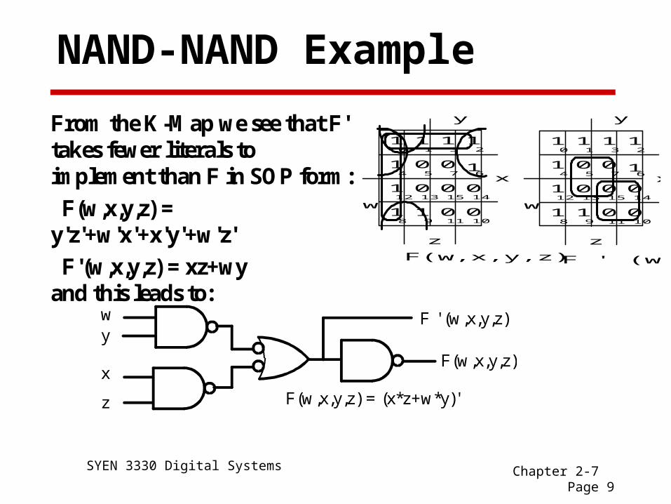
NAND-NAND Example
x
y
z
w
0 1 3 2
4 5 7 6
12 13 15 14
8 9 11 10
1 1 1 1
11
1
1 1
0 0
0 0 0
0 0
x
z
w
0 1 3 2
4 5 7 6
12 13 15 14
8 9 11 10
1 1 1 1
11
1
1 1
0 0
0 0 0
0 0
y
F(w,x,y,z) F ' (w,x,y,z)
From the K-Map we see that F' takes fewer literals to implement than F in SOP form:
F(w,x,y,z) = y'z'+w'x'+x'y'+w'z'
F'(w,x,y,z) = xz+wy and this leads to:
F(w,x,y,z) = (x*z+w*y)'
F(w,x,y,z)
wy
x
z
F ' (w,x,y,z)
SYEN 3330 Digital Systems Chapter 2-7 Page 10
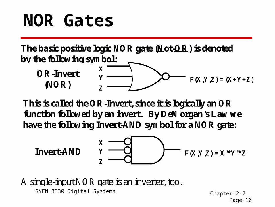
NOR Gates
The basic positive logic NOR gate (Not-OR) is denoted by the following symbol:
XY
ZF(X,Y,Z) = (X+Y+Z)'
OR-Invert (NOR)
This is called the OR-Invert, since it is logically an OR function followed by an invert. By DeMorgan's Law we have the following Invert-AND symbol for a NOR gate:
XY
ZF(X,Y,Z) = X'*Y'*Z'Invert-AND
A single-input NOR gate is an inverter, too.
SYEN 3330 Digital Systems Chapter 2-7 Page 11
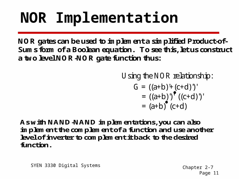
NOR ImplementationNOR gates can be used to implement a simplified Product-of-Sums form of a Boolean equation. To see this, let us construct a two level NOR-NOR gate function thus:
Using the NOR relationship:
G = ((a+b)'+(c+d)')' = ((a+b)')'((c+d)')' = (a+b)(c+d)
As with NAND-NAND implementations, you can also implement the complement of a function and use another level of inverter to complement it back to the desired function.
SYEN 3330 Digital Systems Chapter 2-7 Page 12
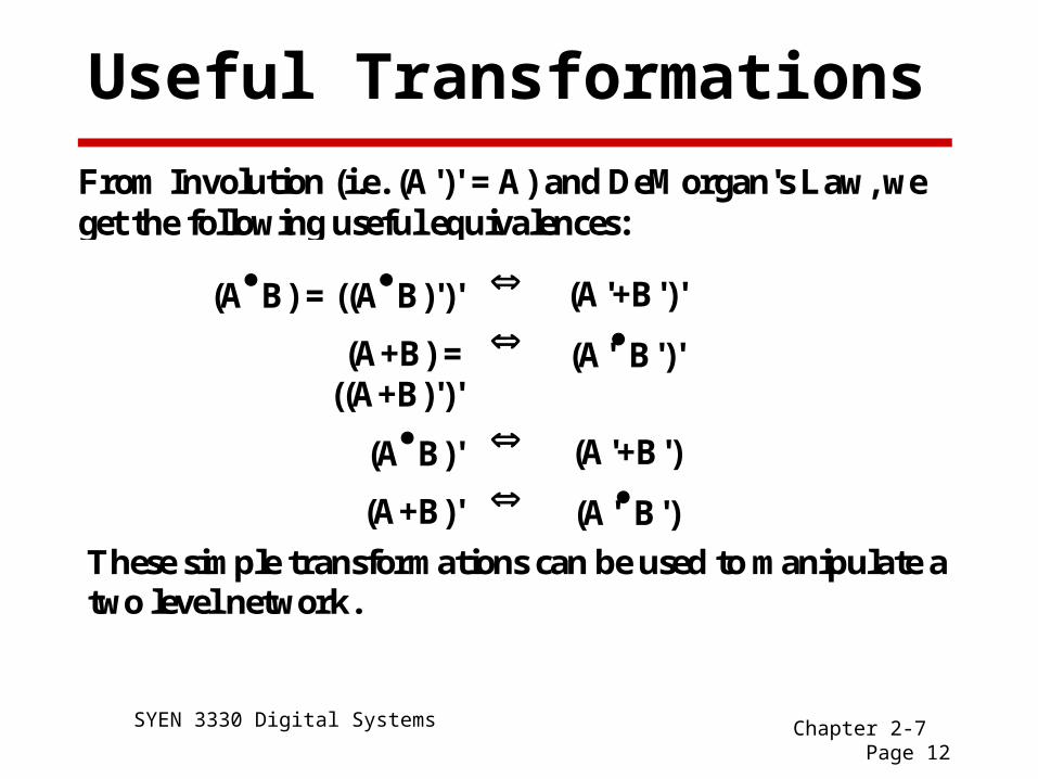
Useful Transformations
From Involution (i.e. (A')' = A) and DeMorgan's Law, we get the following useful equivalences:
(AB) = ((AB)')' (A'+B')'
(A+B) = ((A+B)')'
(A'B')'
(AB)' (A'+B')
(A+B)' (A'B') These simple transformations can be used to manipulate a
two level network.

SYEN 3330 Digital Systems Chapter 2-7 Page 13
Graphical Transformations
The relations from the previous slide lead to the following transformations:
Also, two complement bubbles in series can be removed from the network.
(AB) = ((AB)')' (A'+B')'
(A+B) = ((A+B)')'
(A'B')'
(AB)' (A'+B')
(A+B)' (A'B')
SYEN 3330 Digital Systems Chapter 2-7 Page 14
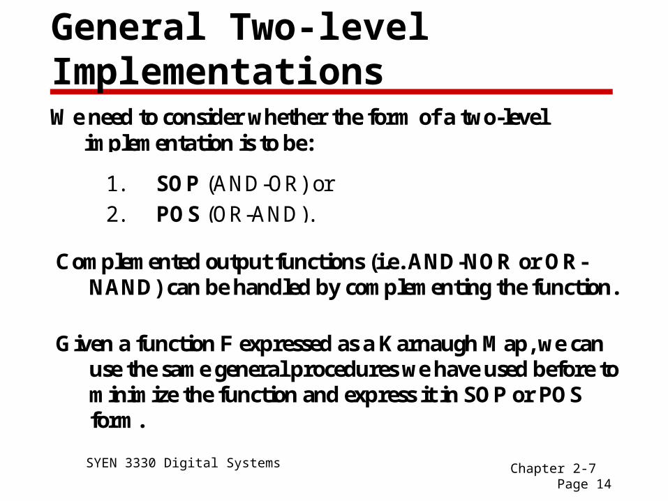
General Two-level Implementations
We need to consider whether the form of a two-level implementation is to be:
1. SOP (AND-OR) or
2. POS (OR-AND).
Complemented output functions (i.e. AND-NOR or OR-NAND) can be handled by complementing the function.
Given a function F expressed as a Karnaugh Map, we can use the same general procedures we have used before to minimize the function and express it in SOP or POS form.
SYEN 3330 Digital Systems Chapter 2-7 Page 15
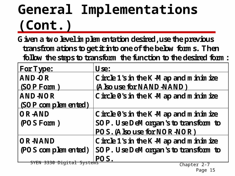
General Implementations (Cont.)
Given a two level implementation desired, use the previous transfromations to get it into one of the below forms. Then follow the steps to transform the function to the desired form:
For Type: Use: AND-OR (SOP Form)
Circle 1's in the K-Map and minimize (Also use for NAND-NAND)
AND-NOR (SOP complemented)
Circle 0's in the K-Map and minimize
OR-AND (POS Form)
Circle 0's in the K-Map and minimize SOP. Use DeMorgan's to transform to POS. (Also use for NOR-NOR)
OR-NAND (POS complemented)
Circle 1's in the K-Map and minimize SOP. Use DeMorgan's to transform to POS.

SYEN 3330 Digital Systems Chapter 2-7 Page 16
Implementation Example
Implement the function in NOR-OR. This transforms to OR-NAND, a POS form with the output variable complemented, so we want to implement the complement of F in POS form. Circle the 1's and minimize:
A
B
C
1
1
1
1
10
0 0
A
B
C
1
1
1
1
10
0 0
F = B' + A'C' Use DeMorgan's Law:
F' = B(A+C)
We can remove the "Inverter" and replace it with the complement of the input variable
SYEN 3330 Digital Systems Chapter 2-7 Page 17
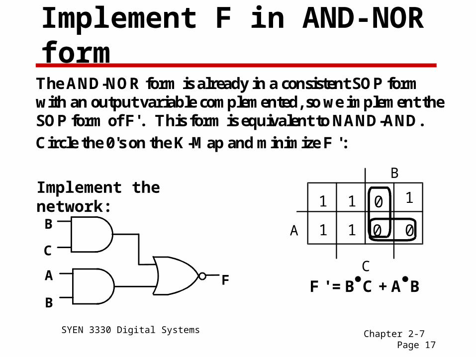
Implement F in AND-NOR form
The AND-NOR form is already in a consistent SOP form with an output variable complemented, so we implement the SOP form of F'. This form is equivalent to NAND-AND.
Circle the 0's on the K-Map and minimize F ':
A
B
C
1
1
1
1
10
0 0
F ' = BC + AB F
C
B
A
B
Implement the network:

SYEN 3330 Digital Systems Chapter 2-7 Page 18
Multi-level NAND Implementations
• Add inverters in two-level implementation into the cost picture
• Attempt to “combine” inverters to reduce the term count
• Attempt to reduce literal + term count by factoring expression into POSOP or SOPOS
SYEN 3330 Digital Systems Chapter 2-7 Page 19
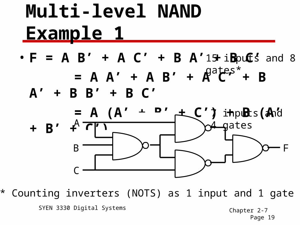
Multi-level NAND Example 1
• F = A B’ + A C’ + B A’ + B C’
= A A’ + A B’ + A C’ + B A’ + B B’ + B C’
= A (A’ + B’ + C’) + B (A’ + B’ + C’)
F
A
C
B
7 inputs and 4 gates
15 inputs and 8 gates*
* Counting inverters (NOTS) as 1 input and 1 gate

SYEN 3330 Digital Systems Chapter 2-7 Page 20
Multilevel NAND Example 2
• F = AB + AD’ + BC + CD’ 12 inputs & 5 gates
= A(B + D’) + C(B + D’) 8 inputs & 5 gates
F
A
C
B
D


