772 DOI: 10.13164/re.2015.0772 APPLICATION OF WIRELESS COMMUNICATIONS Symbol Synchronization for SDR Using a Polyphase Filterbank Based on an FPGA Pavel FIALA, Richard LINHART Dept. of Applied Electronics and Telecom., University of West Bohemia, Univerzitní 26, 306 14 Plze , Czech Republic [email protected], [email protected]Abstract. This paper is devoted to the proposal of a highly efficient symbol synchronization subsystem for Software Defined Radio. The proposed feedback phase-locked loop timing synchronizer is suitable for parallel implementation on an FPGA. The polyphase FIR filter simultaneously performs matched-filtering and arbitrary interpolation between acquired samples. Determination of the proper sampling instant is achieved by selecting a suitable poly- phase filterbank using a derived index. This index is deter- mined based on the output either the Zero-Crossing or Gardner Timing Error Detector. The paper will extensively focus on simulation of the proposed synchronization sys- tem. On the basis of this simulation, a complete, fully pipe- lined VHDL description model is created. This model is composed of a fully parallel polyphase filterbank based on distributed arithmetic, timing error detector and interpola- tion control block. Finally, RTL synthesis on an Altera Cyclone IV FPGA is presented and resource utilization in comparison with a conventional model is analyzed. Keywords Digital communication, digital filters, FPGA, signal processing, synchronization, VHDL 1. Introduction The increasing popularity of Software Defined Radio (SDR) in recent years is forcing complex digital signal processing blocks to be implemented in parallel design flow on an FPGA or ASIC. FPGA technology has under- gone rapid evolution in the last decade and low-end gate arrays like the Altera Cyclone IV are now available for Digital Signal Processing (DSP) at a reasonable price. Symbol synchronization and carrier synchronization are crucial digital receiver blocks. Symbol synchronization is the method of estimating a clock signal, aligned in phase and frequency with the clock signal generated at the trans- mitter side [1]. The clock must be extracted from the re- ceived (noisy) signal because it is not efficient at allocating the spectrum for next the channel, which carries clock information only. Synchronization can be performed using polyphase filter banks, which allow greater flexibility and efficiency in the receiver by computing only those multi- plications necessary for matched filtering, while simultane- ously interpolating in order to achieve a sample point suffi- ciently close to the optimum [2]. The application of the polyphase filter to perform the desired interpolation required for symbol synchronization in general was presented in [1], using the Maximum Like- lihood (ML) approach. The ML timing error detector re- quires the Matched Filter and the Derivative Matched Filter to operate correctly. This approach was further expanded upon by the authors of [2], [3] and [4]. In our work we utilize a Zero-Crossing or Gardner Timing Error Detector, which do not need a derivative matched filter. We also pay particular attention to the polyphase FIR filterbank because this structure has a significant impact on performance of the overall system. The new architecture presented in this paper can be thought of as the significant evolution of symbol synchronization for high-performance digital re- ceivers and demonstrates the deployment of distributed arithmetic. This method is well suited for fixed-point im- plementation within FPGAs and ASICs. This paper is organized as follows. In Sec. 2 we dis- cuss the symbol timing techniques and definitions assumed in this paper, respectively. In Sec. 3 we describe each part of the proposed synchronization system and VHDL de- scription is also provided. In Sec. 4 we present experi- mental results obtained from simulations. The second part of this section deals with the RTL synthesis, the usage of the system resources are discussed. Section 5 is devoted to conclusions. 2. Symbol Timing Recovery The symbol synchronization loop can generally ac- commodate either a feed-forward or feedback structure. The first variant is frequently used in packetized burst communication and relies on a sequence of known sym- bols. Additional classification can be carried out according to their treatment of the following two data categories: Data-Aided and Non-Data-Aided (NDA) methods [5]. The Data-Aided method assumes that transmitted symbols (a training sequence) are known. Decision-Directed (DD) technique, a special subcategory of Data-Aided, is a tech- nique where decoded symbols are used for decision mak- ing. This paper further focuses on feedback (digital) Phase- P. FIALA, R. LINHART, SYMBOL SYNCHRONIZATION FOR SDR USING A POLYPHASE FILTER BANK BASED ON AN FPGA
Transcript
772 P. FIALA, R. LINHART, SYMBOL SYNCHRONIZATION FOR SDR USING A POLYPHASE FILTER BANK BASED ON FPGA
DOI: 10.13164/re.2015.0772 APPLICATION OF WIRELESS COMMUNICATIONS
Symbol Synchronization for SDR Using a Polyphase Filterbank Based on an FPGA
Pavel FIALA, Richard LINHART
Dept. of Applied Electronics and Telecom., University of West Bohemia, Univerzitní 26, 306 14 Plze , Czech Republic
Abstract. This paper is devoted to the proposal of a highly efficient symbol synchronization subsystem for Software Defined Radio. The proposed feedback phase-locked loop timing synchronizer is suitable for parallel implementation on an FPGA. The polyphase FIR filter simultaneously performs matched-filtering and arbitrary interpolation between acquired samples. Determination of the proper sampling instant is achieved by selecting a suitable poly-phase filterbank using a derived index. This index is deter-mined based on the output either the Zero-Crossing or Gardner Timing Error Detector. The paper will extensively focus on simulation of the proposed synchronization sys-tem. On the basis of this simulation, a complete, fully pipe-lined VHDL description model is created. This model is composed of a fully parallel polyphase filterbank based on distributed arithmetic, timing error detector and interpola-tion control block. Finally, RTL synthesis on an Altera Cyclone IV FPGA is presented and resource utilization in comparison with a conventional model is analyzed.
Keywords Digital communication, digital filters, FPGA, signal processing, synchronization, VHDL
1. Introduction The increasing popularity of Software Defined Radio
(SDR) in recent years is forcing complex digital signal processing blocks to be implemented in parallel design flow on an FPGA or ASIC. FPGA technology has under-gone rapid evolution in the last decade and low-end gate arrays like the Altera Cyclone IV are now available for Digital Signal Processing (DSP) at a reasonable price. Symbol synchronization and carrier synchronization are crucial digital receiver blocks. Symbol synchronization is the method of estimating a clock signal, aligned in phase and frequency with the clock signal generated at the trans-mitter side [1]. The clock must be extracted from the re-ceived (noisy) signal because it is not efficient at allocating the spectrum for next the channel, which carries clock information only. Synchronization can be performed using polyphase filter banks, which allow greater flexibility and efficiency in the receiver by computing only those multi-
plications necessary for matched filtering, while simultane-ously interpolating in order to achieve a sample point suffi-ciently close to the optimum [2].
The application of the polyphase filter to perform the desired interpolation required for symbol synchronization in general was presented in [1], using the Maximum Like-lihood (ML) approach. The ML timing error detector re-quires the Matched Filter and the Derivative Matched Filter to operate correctly. This approach was further expanded upon by the authors of [2], [3] and [4]. In our work we utilize a Zero-Crossing or Gardner Timing Error Detector, which do not need a derivative matched filter. We also pay particular attention to the polyphase FIR filterbank because this structure has a significant impact on performance of the overall system. The new architecture presented in this paper can be thought of as the significant evolution of symbol synchronization for high-performance digital re-ceivers and demonstrates the deployment of distributed arithmetic. This method is well suited for fixed-point im-plementation within FPGAs and ASICs.
This paper is organized as follows. In Sec. 2 we dis-cuss the symbol timing techniques and definitions assumed in this paper, respectively. In Sec. 3 we describe each part of the proposed synchronization system and VHDL de-scription is also provided. In Sec. 4 we present experi-mental results obtained from simulations. The second part of this section deals with the RTL synthesis, the usage of the system resources are discussed. Section 5 is devoted to conclusions.
2. Symbol Timing Recovery The symbol synchronization loop can generally ac-
commodate either a feed-forward or feedback structure. The first variant is frequently used in packetized burst communication and relies on a sequence of known sym-bols. Additional classification can be carried out according to their treatment of the following two data categories: Data-Aided and Non-Data-Aided (NDA) methods [5]. The Data-Aided method assumes that transmitted symbols (a training sequence) are known. Decision-Directed (DD) technique, a special subcategory of Data-Aided, is a tech-nique where decoded symbols are used for decision mak-ing. This paper further focuses on feedback (digital) Phase-
P. FIALA, R. LINHART, SYMBOL SYNCHRONIZATION FOR SDR USING A POLYPHASE FILTER BANK BASED ON AN FPGA
RADIOENGINEERING, VOL. 24, NO. 3, SEPTEMBER 2015 773
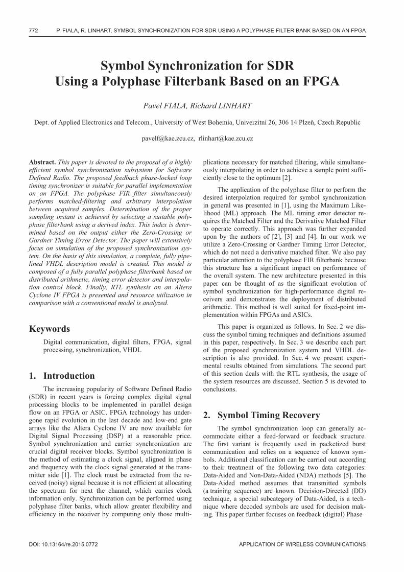
Fig. 1. Block diagram of a discrete feedback PLL timing loop.
locked loop (PLL) NDA/DD synchronization methods for the software defined m-QAM receiver. Figure 1 shows the conventional feedback PLL DSP approach to symbol syn-chronization.
The samples labeled x(n) are initially processed in the Matched Filter (MF) and the interpolation filter calculates samples y(k) at the desired positions from the offset sam-ples provided by the free-running ADC. These position corrected samples are used by the timing error detector to form the timing error signal e(k). The interpolation control section estimates the coefficients (namely, the fractional interval μk [6]) of the interpolation filter via the filtered error signal.
The timing error detector plays an important role in the synchronization system because the overall architecture of this timing loop depends on it. We have chosen to use a Zero-Crossing Timing Error Detector (ZCTED). The ZCTED is based on determining zero crossing in the eye diagram. It operates using 2 samples / symbol and produces zero error when every other sample is time-aligned with zero crossing in the matched filter output [6]. We assume that the matched filter produces outputs at a rate of 2 sam-ples / symbol and are indexed by the symbol index k:
( )( ) ( )( ) ( )( )( ) ( )( )
, 1 , 1 / 2 , ,
1 / 2 , 1 ,s s s
s s
x k T x k T x kT
x k T x k T
τ τ τ
τ
… − − − − −
+ − + … (1)
The timing error signal e(k) can then be expressed as
( ) ( )( ) ( ) ( )1 2 1ˆ/ZCTED se k x k T a k a kτ= − + − − (2)
where Ts is the sampling period (the sample clock is inde-pendent of the data clock used by the transmitter); is the timing offset; is the timing delay estimate for the detector and symbol decisions a for the DD detector are
( ) ( )( )( ) ( )
1 sgn 1 ,
sgn
ˆ
ˆ .
s
s
a k x k T
a k x kT
τ
τ
− = − +
= + (3)
Special modification of the ZCTED is called Gardner Timing Error Detector (GTED). This exclusively NDA detector is independent of any carrier phase rotation and can be placed before the carrier synchronization subsystem [6]. It also operates using 2 samples / symbol where the error signal e(k) is
( ) ( )( )( )( ) ( )
ˆ
ˆ ˆ
1 / 2
1 .
GTED s
s s
e k x k T
x k T x kT
τ
τ τ
= − +
− + − + (4)
Polyphase filter decomposition is useful when imple-menting decimation or interpolation. This approach can be applied to symbol synchronization using an upsample filter performed solely by a polyphase filterbank (or else by a polyphase interpolator). The discrete impulse response of the m-th filter in the bank of M filters is given by [2]
( )m s s smh mT h nT TM
= + . (5)
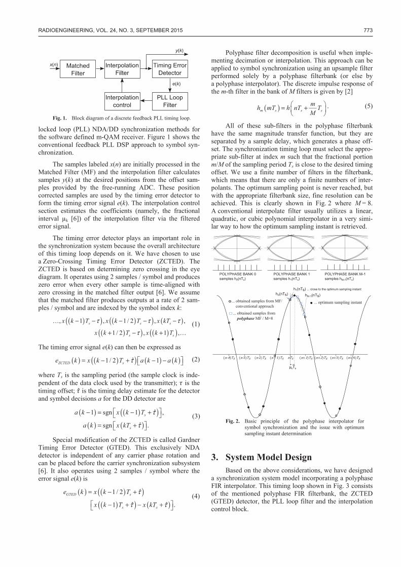
All of these sub-filters in the polyphase filterbank have the same magnitude transfer function, but they are separated by a sample delay, which generates a phase off-set. The synchronization timing loop must select the appro-priate sub-filter at index m such that the fractional portion m/M of the sampling period Ts is close to the desired timing offset. We use a finite number of filters in the filterbank, which means that there are only a finite numbers of inter-polants. The optimum sampling point is never reached, but with the appropriate filterbank size, fine resolution can be achieved. This is clearly shown in Fig. 2 where M = 8. A conventional interpolate filter usually utilizes a linear, quadratic, or cubic polynomial interpolator in a very simi-lar way to how the optimum sampling instant is retrieved.
Fig. 2. Basic principle of the polyphase interpolator for
symbol synchronization and the issue with optimum sampling instant determination
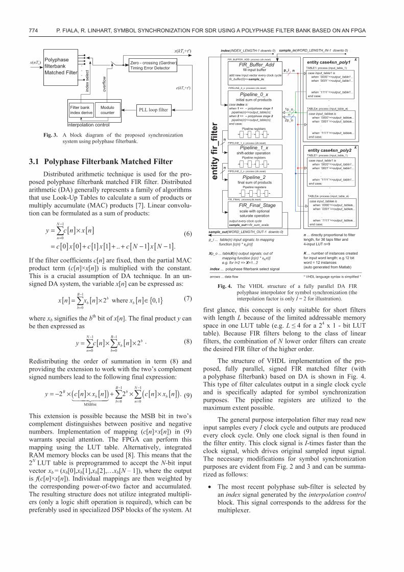
3. System Model Design Based on the above considerations, we have designed
a synchronization system model incorporating a polyphase FIR interpolator. This timing loop shown in Fig. 3 consists of the mentioned polyphase FIR filterbank, the ZCTED (GTED) detector, the PLL loop filter and the interpolation control block.
774 P. FIALA, R. LINHART, SYMBOL SYNCHRONIZATION FOR SDR USING A POLYPHASE FILTER BANK BASED ON FPGA
Fig. 3. A block diagram of the proposed synchronization
system using polyphase filterbank.
3.1 Polyphase Filterbank Matched Filter Distributed arithmetic technique is used for the pro-
posed polyphase filterbank matched FIR filter. Distributed arithmetic (DA) generally represents a family of algorithms that use Look-Up Tables to calculate a sum of products or multiply accumulate (MAC) products [7]. Linear convolu-tion can be formulated as a sum of products:
[ ] [ ]
[ ] [ ] [ ] [ ] [ ] [ ]
1
0
0 0 1 1 .. 1 1 .
N
n
y c n x n
c x c x c N x N
−
=
= ×
= + + + − −
(6)
If the filter coefficients c[n] are fixed, then the partial MAC product term (c[n]×x[n]) is multiplied with the constant. This is a crucial assumption of DA technique. In an un-signed DA system, the variable x[n] can be expressed as:
[ ] [ ] [ ] { }1
0
2 where 0,1B
bb b
b
x n x n x n−
=
= × ∈ (7)
where xb signifies the bth bit of x[n]. The final product y can be then expressed as
[ ] [ ]1 1
0 0
2 N B
bb
n b
y c n x n− −
= =
= × × . (8)
Redistributing the order of summation in term (8) and providing the extension to work with the two’s complement signed numbers lead to the following final expression:
[ ] [ ]( ) [ ] [ ]( )1 1
0 0MSBbit
2 2 . B N
B bb b
b n
y c n x n c n x n− −
= =
= − × × + × × (9)
This extension is possible because the MSB bit in two’s complement distinguishes between positive and negative numbers. Implementation of mapping (c[n]×x[n]) in (9) warrants special attention. The FPGA can perform this mapping using the LUT table. Alternatively, integrated RAM memory blocks can be used [8]. This means that the 2N LUT table is preprogrammed to accept the N-bit input vector xb = (xb[0],xb[1],xb[2],…xb[N – 1]), where the output is f(c[n]×x[n]). Individual mappings are then weighted by the corresponding power-of-two factor and accumulated. The resulting structure does not utilize integrated multipli-ers (only a logic shift operation is required), which can be preferably used in specialized DSP blocks of the system. At
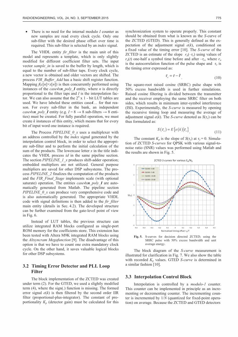
Fig. 4. The VHDL structure of a fully parallel DA FIR
polyphase interpolator for symbol synchronization (the interpolation factor is only I = 2 for illustration).
first glance, this concept is only suitable for short filters with length L because of the limited addressable memory space in one LUT table (e.g. L 4 for a 24 x 1 - bit LUT table). Because FIR filters belong to the class of linear filters, the combination of N lower order filters can create the desired FIR filter of the higher order.
The structure of VHDL implementation of the pro-posed, fully parallel, signed FIR matched filter (with a polyphase filterbank) based on DA is shown in Fig. 4. This type of filter calculates output in a single clock cycle and is specifically adapted for symbol synchronization purposes. The pipeline registers are utilized to the maximum extent possible.
The general purpose interpolation filter may read new input samples every I clock cycle and outputs are produced every clock cycle. Only one clock signal is then found in the filter entity. This clock signal is I-times faster than the clock signal, which drives original sampled input signal. The necessary modifications for symbol synchronization purposes are evident from Fig. 2 and 3 and can be summa-rized as follows:
• The most recent polyphase sub-filter is selected by an index signal generated by the interpolation control block. This signal corresponds to the address for the multiplexer.
P. FIALA, R. LINHART, SYMBOL SYNCHRONIZATION FOR SDR USING A POLYPHASE FILTER BANK BASED ON AN FPGA
RADIOENGINEERING, VOL. 24, NO. 3, SEPTEMBER 2015 775
• There is no need for the internal modulo I counter as new samples are read every clock cycle. Only one sub-filter with the desired phase offset over time is required. This sub-filter is selected by an index signal.
The VHDL entity fir_filter is the main unit of this model and represents a template, which is only slightly modified for different coefficient filter sets. The input vector sample_in is saved to the buffer by length, which is equal to the number of sub-filter taps. Every clock cycle, a new vector is obtained and older vectors are shifted. The process FIR_Buffer_Add has a basic shift register function. Mapping f(c[n]×x[n]) is then concurrently performed using instances of the case4xn_poly_I entity, where n is directly proportional to the filter taps and I is the interpolation fac-tor. We can also assume that the 24 x 1 - bit LUT tables are used. We have labeled these entities case4… for that rea-son. For every sub-filter in the bank, an independent case4xn_poly_I entity (e.g. I = 8 8 sub-filters 8 enti-ties) must be created. For fully parallel operation, we must create k instances of this entity, which means that for every bit of input word one instance is required.
The Process PIPELINE_0_x uses a multiplexer with an address controlled by the index signal generated by the interpolation control block, in order to select the appropri-ate sub-filter and to perform the initial calculation of the sum of the products. The lowercase letter x in the title indi-cates the VHDL process id in the same pipeline section. The section PIPELINE_1_x produces shift-adder operation; embedded multipliers are not utilized. General purpose multipliers are saved for other DSP subsystems. The pro-cess PIPELINE_2 finalizes the computation of the products and the FIR_Final_Stage implements scale (with optional saturate) operation. The entities case4xn_poly_I are auto-matically generated from Matlab. The pipeline section PIPELINE_0_x can produce very comprehensive code and is also automatically generated. The appropriate VHDL code with signal definitions is then added to the fir_filter main entity (details in Sec. 4.2). The developed structure can be further examined from the gate-level point of view in Fig. 6.
Instead of LUT tables, the previous structure can utilize integrated RAM blocks configured as single-port ROM memory for the coefficients store. This extension has been tested with Altera M9K integrated RAM blocks using the Altsyncram Megafunction [9]. The disadvantage of this option is that we have to count one extra mandatory clock cycle. On the other hand, it saves valuable logical blocks for other DSP subsystems.
3.2 Timing Error Detector and PLL Loop Filter The block implementation of the ZCTED was created
under term (2). For the GTED, we used a slightly modified term (4), where the sign(.) function is missing. The formed error signal e(k) is then filtered by the second order IIR filter (proportional-plus-integrator). The constant of pro-portionality Kp (detector gain) must be calculated for this
synchronization system to operate properly. This constant should be obtained from what is known as the S-curve of the ZCTED (GTED). This is generally defined as the ex-pectation of the adjustment signal e(k), conditioned on a fixed value of the timing error [10]. The S-curve of the ZCTED is an estimate of the slope ra(– e) using values of ra(t) one-half a symbol time before and after – e, where ra is the autocorrelation function of the pulse shape and e is the timing error expressed as:
ˆeτ τ τ= − . (10)
The square-root raised cosine (SRRC) pulse shape with 50% excess bandwidth is used in further simulations. Raised cosine filtering is divided between the transmitter and the receiver employing the same SRRC filter on both sides, which results in minimum inter-symbol interference (ISI). Experimentally, the S-curve is measured by opening the recursive timing loop and measuring the average of adjustment signal e(k). The S-curve denoted as S( e) can be thus formulated as:
( ) ( ){ }e eS E e kτ τ= . (11)
The constant Kp is the slope of S( e) at e = 0. Simula-tion of ZCTED S-curves for QPSK with various signal-to-noise ratio (SNR) values was performed using Matlab and the results are shown in Fig. 5.
Fig. 5. S-curves for decision directed ZCTED; using the
SRRC pulse with 50% excess bandwidth and unit average energy.
The block diagram of the S-curve measurement is illustrated for clarification in Fig. 7. We also show the table with recorded Kp values. GTED S-curve is determined in a similar fashion [10].
3.3 Interpolation Control Block Interpolation is controlled by a modulo-1 counter.
This counter can be implemented in principle as an incre-menting or decrementing counter. The incrementing coun-ter is incremented by 1/N (quantized for fixed-point opera-tion) on average. Because the ZCTED and GTED detectors
-3
-2
-1
0
1
2
3
-0,5 -0,4 -0,3 -0,2 -0,1 0 0,1 0,2 0,3 0,4 0,5
S( e)
Normalized timing offset e/T
ZCTED S-curves for various Eb/N0
Eb/N0= 0 dB
Eb/N0= 5 dB
Eb/N0= 10 dB
Eb/N0= 20 dB
776 P. FIALA, R. LINHART, SYMBOL SYNCHRONIZATION FOR SDR USING A POLYPHASE FILTER BANK BASED ON FPGA
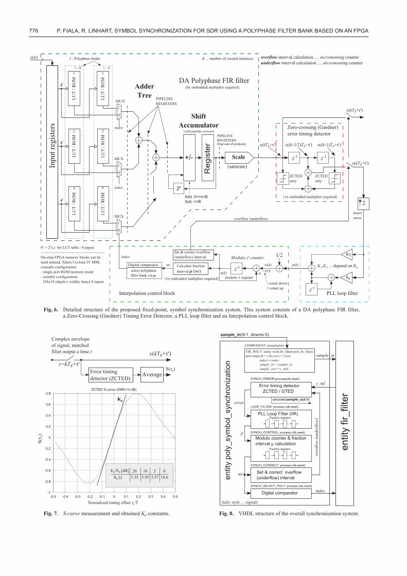
Fig. 6. Detailed structure of the proposed fixed-point, symbol synchronization system. This system consists of a DA polyphase FIR filter,
a Zero-Crossing (Gardner) Timing Error Detector, a PLL loop filter and an Interpolation control block.
Fig. 7. S-curve measurement and obtained Kp constants.
Fig. 8. VHDL structure of the overall synchronization system.
P. FIALA, R. LINHART, SYMBOL SYNCHRONIZATION FOR SDR USING A POLYPHASE FILTER BANK BASED ON AN FPGA
RADIOENGINEERING, VOL. 24, NO. 3, SEPTEMBER 2015 777
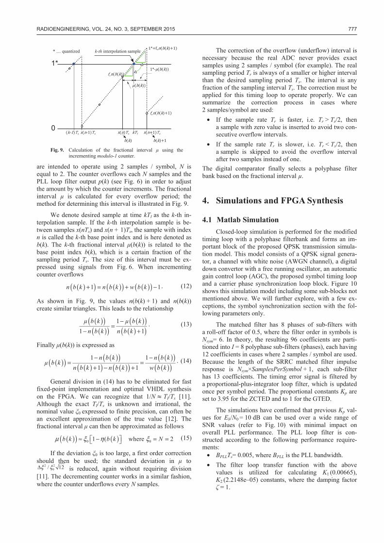
Fig. 9. Calculation of the fractional interval μ using the
incrementing modulo-1 counter.
are intended to operate using 2 samples / symbol, N is equal to 2. The counter overflows each N samples and the PLL loop filter output p(k) (see Fig. 6) in order to adjust the amount by which the counter increments. The fractional interval μ is calculated for every overflow period; the method for determining this interval is illustrated in Fig. 9.
We denote desired sample at time kTI as the k-th in-terpolation sample. If the k-th interpolation sample is be-tween samples x(nTs) and x(n + 1)Ts, the sample with index n is called the k-th base point index and is here denoted as b(k). The k-th fractional interval (b(k)) is related to the base point index b(k), which is a certain fraction of the sampling period Ts. The size of this interval must be ex-pressed using signals from Fig. 6. When incrementing counter overflows
( )( ) ( )( ) ( )( )1 1n b k n b k w b k+ = + − . (12)
As shown in Fig. 9, the values n(b(k) + 1) and n(b(k)) create similar triangles. This leads to the relationship
( )( )( )( )
( )( )( )( )
11 1μ b k μ b k
n b k n b k−
=− +
. (13)
Finally (b(k)) is expressed as
( )( ) ( )( )( )( ) ( )( )
( )( )( )( )
1 11 1n b k n b k
μ b kn b k n b k w b k
− −= =
+ − +. (14)
General division in (14) has to be eliminated for fast fixed-point implementation and optimal VHDL synthesis on the FPGA. We can recognize that 1/N TI/Ts [11]. Although the exact TI/Ts is unknown and irrational, the nominal value 0 expressed to finite precision, can often be an excellent approximation of the true value [12]. The fractional interval can then be approximated as follows
( )( ) ( )0 01 ( where 2b k b k Nμ ξ η ξ≈ − = = (15)
If the deviation 0 is too large, a first order correction should then be used; the standard deviation in to
2 20/ 12ξ ξΔ is reduced, again without requiring division
[11]. The decrementing counter works in a similar fashion, where the counter underflows every N samples.
The correction of the overflow (underflow) interval is necessary because the real ADC never provides exact samples using 2 samples / symbol (for example). The real sampling period Tr is always of a smaller or higher interval than the desired sampling period Ts. The interval is any fraction of the sampling interval Ts. The correction must be applied for this timing loop to operate properly. We can summarize the correction process in cases where 2 samples/symbol are used: • If the sample rate Tr is faster, i.e. Tr > Ts/2, then
a sample with zero value is inserted to avoid two con-secutive overflow intervals.
• If the sample rate Tr is slower, i.e. Tr < Ts/2, then a sample is skipped to avoid the overflow interval after two samples instead of one.
The digital comparator finally selects a polyphase filter bank based on the fractional interval μ.
4. Simulations and FPGA Synthesis
4.1 Matlab Simulation Closed-loop simulation is performed for the modified
timing loop with a polyphase filterbank and forms an im-portant block of the proposed QPSK transmission simula-tion model. This model consists of a QPSK signal genera-tor, a channel with white noise (AWGN channel), a digital down convertor with a free running oscillator, an automatic gain control loop (AGC), the proposed symbol timing loop and a carrier phase synchronization loop block. Figure 10 shows this simulation model including some sub-blocks not mentioned above. We will further explore, with a few ex-ceptions, the symbol synchronization section with the fol-lowing parameters only.
The matched filter has 8 phases of sub-filters with a roll-off factor of 0.5, where the filter order in symbols is Nsym= 6. In theory, the resulting 96 coefficients are parti-tioned into I = 8 polyphase sub-filters (phases), each having 12 coefficients in cases where 2 samples / symbol are used. Because the length of the SRRC matched filter impulse response is Nsym×SamplesPerSymbol + 1, each sub-filter has 13 coefficients. The timing error signal is filtered by a proportional-plus-integrator loop filter, which is updated once per symbol period. The proportional constants Kp are set to 3.95 for the ZCTED and to 1 for the GTED.
The simulations have confirmed that previous Kp val-ues for Eb/N0 = 10 dB can be used over a wide range of SNR values (refer to Fig. 10) with minimal impact on overall PLL performance. The PLL loop filter is con-structed according to the following performance require-ments: • BPLLTs= 0.005, where BPLL is the PLL bandwidth. • The filter loop transfer function with the above
values is utilized for calculating K1 (0.00665), K2 (2.2148e–05) constants, where the damping factor = 1.
778 P. FIALA, R. LINHART, SYMBOL SYNCHRONIZATION FOR SDR USING A POLYPHASE FILTER BANK BASED ON FPGA
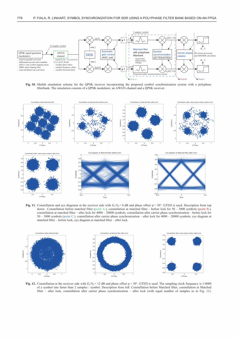
Fig. 10. Matlab simulation scheme for the QPSK receiver incorporating the proposed symbol synchronization system with a polyphase
filterbank. The simulation consists of a QPSK modulator, an AWGN channel and a QPSK receiver.
Fig. 11. Constellation and eye diagrams at the receiver side with Eb/N0 = 8 dB and phase offset = 30°. GTED is used. Description from top
down: Constellation before matched filter (point A.), constellation at matched filter – before lock for 50 – 3000 symbols (point B.), constellation at matched filter – after lock for 4000 – 20000 symbols, constellation after carrier phase synchronization – before lock for 50 – 3000 symbols (point C.), constellation after carrier phase synchronization – after lock for 4000 – 20000 symbols, eye diagram at matched filter – before lock, eye diagram at matched filter – after lock.
Fig. 12. Constellation at the receiver side with Eb/N0 = 12 dB and phase offset = 30°. GTED is used. The sampling clock frequency is 1/4000 of a symbol rate faster than 2 samples / symbol. Description from left: Constellation before Matched filter, constellation at Matched filter – after lock, constellation after carrier phase synchronization – after lock (with equal number of samples as in Fig. 11).
-1 -0.5 0 0.5 1
-1
-0.5
0
0.5
1
Qua
drat
ure
In-Phase
Constellation before Matched filter
-1 -0.5 0 0.5 1
-1
-0.5
0
0.5
1
Qua
drat
ure
In-Phase
Constellation at Matched filter (before lock)
-1 -0.5 0 0.5 1
-1
-0.8
-0.6
-0.4
-0.2
0
0.2
0.4
0.6
0.8
1
Qua
drat
ure
In-Phase
Constellation at Matched filter (after lock)
-1 -0.5 0 0.5 1
-1
-0.5
0
0.5
1
Qua
drat
ure
In-Phase
Constellation after carrier phase rotation (before lock)
-0.5 0 0.5
-0.8
-0.6
-0.4
-0.2
0
0.2
0.4
0.6
0.8
Qua
drat
ure
In-Phase
Constellation after carrier phase rotation (after lock)
-0.5 0 0.5-1
-0.8
-0.6
-0.4
-0.2
0
0.2
0.4
0.6
0.8
1
Time
Am
plitu
de
Eye diagram at Matched filter (before lock)
-0.5 0 0.5-0.8
-0.6
-0.4
-0.2
0
0.2
0.4
0.6
0.8
Time
Am
plitu
deEye diagram at Matched filter (after lock)
-1 -0.5 0 0.5 1
-1
-0.5
0
0.5
1
Qua
drat
ure
In-Phase
Constellation before Matched filter
-1 -0.5 0 0.5 1-1
-0.8
-0.6
-0.4
-0.2
0
0.2
0.4
0.6
0.8
1
Qua
drat
ure
In-Phase
Constellation at Matched filter (after lock)
-0.5 0 0.5-0.8
-0.6
-0.4
-0.2
0
0.2
0.4
0.6
0.8
Qua
drat
ure
In-Phase
Constellation after carrier phase rotation (after lock)
P. FIALA, R. LINHART, SYMBOL SYNCHRONIZATION FOR SDR USING A POLYPHASE FILTER BANK BASED ON AN FPGA
RADIOENGINEERING, VOL. 24, NO. 3, SEPTEMBER 2015 779
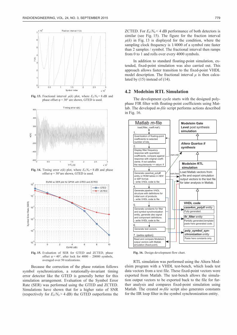
Fig. 13. Fractional interval μ(k) plot, where Eb/N0 = 8 dB and
phase offset = 30° are shown, GTED is used.
Fig. 14. Timing error e(k) plot, where Eb/N0 = 8 dB and phase
offset = 30°are shown, GTED is used.
Fig. 15. Evaluation of SER for GTED and ZCTED, phase
offset = 40°, after lock for 4000 – 20000 symbols, averaged over 50 realizations.
Because the correction of the phase rotation follows symbol synchronization, a rotationally-invariant timing error detector like the GTED is generally better for this simulation arrangement. Evaluation of the Symbol Error Rate (SER) was performed using the GTED and ZCTED. Simulations have shown that for a higher ratio of SNR (respectively for Eb/N0 > 4 dB) the GTED outperforms the
ZCTED. For Eb/N0 < 4 dB performance of both detectors is similar (see Fig. 15). The figure for the fraction interval μ(k) in Fig. 13 is displayed for the condition, where the sampling clock frequency is 1/4000 of a symbol rate faster than 2 samples / symbol. The fractional interval then ramps from 0 to 1 and rolls over every 4000 symbols.
In addition to standard floating-point simulation, ex-tended, fixed-point simulation was also carried out. This approach allows faster transition to the fixed-point VHDL model description. The fractional interval is then calcu-lated by (15) instead of (14).
4.2 Modelsim RTL Simulation The development cycle starts with the designed poly-
phase FIR filter with floating-point coefficients using Mat-lab. The developed m-file script performs actions described in Fig. 16.
Fig. 16. Design development flow chart.
RTL simulation was performed using the Altera Mod-elsim program with a VHDL test-bench, which loads test data vectors from a text file. These fixed-point vectors were exported from Matlab. The test-bench allows the simula-tion output vectors to be exported back to the file for fur-ther analysis and compares fixed-point simulation using Matlab. The created m-file script also generates constants for the IIR loop filter in the symbol synchronization entity.
0 0.5 1 1.5 2 2.5 3
x 104
0
1
2
3
4
5
6
7x 10⁴ Fract ion interval 7 (k)
Symbol index
7(k
)
0 0.5 1 1.5 2 2.5 3
x 104
-600
-400
-200
0
200
400
600T iming error e(k)
t=Ts (s)
e(k)
-2 0 2 4 6 8 1010-5
10-4
10-3
10-2
10-1
100
Eb/N0 (dB)
Sym
bol E
rror R
ate
(SE
R)
Eb/N0 vs SER plot for QPSK with GTED and ZCTED
GTEDZCTED
780 P. FIALA, R. LINHART, SYMBOL SYNCHRONIZATION FOR SDR USING A POLYPHASE FILTER BANK BASED ON FPGA
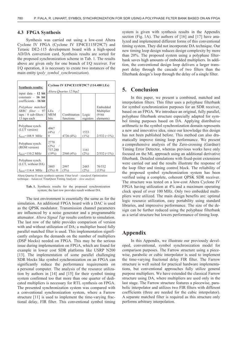
4.3 FPGA Synthesis Synthesis was carried out using a low-cost Altera
Cyclone IV FPGA (Cyclone IV EP4CE115F29C7) and Terasic DE2-115 development board with a high-speed AD/DA conversion card. Synthesis results are sorted for the proposed synchronization scheme in Tab. 1. The results above are given only for one branch of I/Q receiver. For I/Q operation, it is necessary to create two instances of the main entity (poly_symbol_synchronization).
Synthesis results:
input data – 12 bit constants – 16 bit coefficients – 16 bit
Altera Quartus II main synthesis options: Fitter level – standard; Optimization technique – balanced, TimeQuest Timing Analyzer – slow analysis
Tab. 1. Synthesis results for the proposed synchronization system; the last row provides result without DA.
The test environment is essentially the same as for the simulation. An additional FPGA board with a DAC is used as the QPSK modulator. Transmission channel parameters are influenced by a noise generator and a programmable attenuator. Altera Signal Tap results conform to simulation. The last row of the table provides comparison of version with and without utilization of DA; a multiplier based fully parallel matched filter is used. This implementation signifi-cantly enlarges the demands on the number of multipliers (DSP blocks) needed on FPGA. This may be the serious issue during implementation on FPGA, which are found for example in lower cost SDR platforms like USRP N200 [13]. The implementation of some parallel challenging SDR blocks like symbol synchronization on an FPGA can significantly reduce the performance requirements on a personal computer. The analysis of the resource utiliza-tion by authors in [14] and [15] for their symbol timing system confirmed too that more than one quarter of dedi-cated multipliers is necessary for RTL synthesis on FPGA. The presented synchronization system was compared with a conventional synchronization system, where a Farrow structure [11] is used to implement the time-varying frac-tional delay, FIR filter. This conventional symbol timing
system is given with synthesis results in the Appendix section (Fig. 1A). The authors of [16] and [17] have ana-lyzed and implemented different forms of this conventional timing system. They did not incorporate DA technique. Our new timing loop design reduces design complexity by more than 20%. The proposed system using a polyphase filter-bank saves high amounts of embedded multipliers. In addi-tion, the conventional design loop delivers a larger trans-port delay through the cascade of two filters than the filterbank design’s loop through the delay of a single filter.
5. Conclusion In this paper, we present a combined, matched and
interpolation filters. This filter uses a polyphase filterbank for symbol synchronization purposes for an SDR receiver, based on an FPGA. We introduce an original, fully parallel, polyphase filterbank structure especially adapted for sym-bol timing purposes based on DA. Applying distributive arithmetic to the symbol synchronization domain represents a new and innovative idea, since our knowledge this design has not been published before. This method can also dra-matically improve timing loop performance. We present a comprehensive analysis of the Zero-crossing (Gardner) Timing Error Detector, whereas previous works have only focused on the ML approach using an additional derivative filterbank. Detailed simulations with fixed-point extensions were carried out and the results illustrate the response of the loop filter and timing control block. The reliability of the proposed symbol synchronization system has been verified using a complete, coherent QPSK SDR receiver. The structure was tested on a low-cost Altera Cyclone IV FPGA having utilization at 4% and a maximum operating clock speed of over 100 MHz. Only two embedded multi-pliers were utilized. The main design benefits are: optimal logic resource utilization, easy portability using standard libraries, and impressive performance. The size of the de-sign can be further reduced using the polyphase filterbank as a serial structure but lowers performance of timing loop.
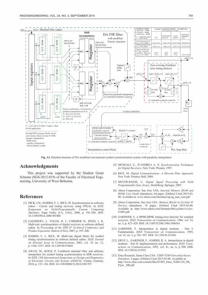
Appendix In this Appendix, we illustrate our previously devel-
oped, conventional, symbol synchronization model for comparison purposes. The Farrow structure using a piece-wise, parabolic or cubic interpolator is used to implement the time-varying fractional delay FIR filter. The Farrow structure is well suited for practical hardware implementa-tions, but conventional approaches fully utilize general purpose multipliers. We have extended the classical Farrow structure using DA, where multipliers are used only in the last stage. The Farrow structure features a piecewise, para-bolic interpolator and utilizes two FIR filters with different coefficients (three are needed for the cubic interpolator). A separate matched filter is required as this structure only performs arbitrary interpolation.
P. FIALA, R. LINHART, SYMBOL SYNCHRONIZATION FOR SDR USING A POLYPHASE FILTER BANK BASED ON AN FPGA
RADIOENGINEERING, VOL. 24, NO. 3, SEPTEMBER 2015 781
Fig. A1. Detailed structure of DA modified conventional symbol synchronization system with parabolic interpolator.
Acknowledgments This project was supported by the Student Grant
Scheme (SGS-2012-019) of the Faculty of Electrical Engi-neering, University of West Bohemia.
References [1] DICK, CH., HARRIS, F. J., RICE, M. Synchronization in software
radios - Carrier and timing recovery using FPGAs. In IEEE Symposium on Field-Programmable Custom Computing Machines. Napa Valley (CA, USA), 2000, p. 195–204. DOI: 10.1109/FPGA.2000.903406
[2] GAEDDERT, J., VOLOS, H. I., CORMIER D., REED, J. H. Multi-rate synchronization of digital receivers in software-defined radios. In Proceeding of the SDR 07 Technical Conference and Product Exposition. Denver (USA), 2007, p. 195–200.
[3] HARRIS, F. J., RICE, M. Multi-rate digital filters for symbol timing synchronization in software defined radios. IEEE Journal on Selected Areas in Communications, 2001, vol. 19, no. 12, p. 2346–2357. DOI: 10.1109/49.974601
[4] AWAN, M., KOCH, P. Combined matched filter and arbitrary interpolator for symbol timing synchronization in SDR receivers. In IEEE 13th International Symposium on Design and Diagnostics of Electronic Circuits and Systems (DDECS). Vienna (Austria), 2010, p. 153–156. DOI: 10.1109/DDECS.2010.5491797
[5] MENGALI, U., D’ANDREA A. N. Synchronization Techniques for Digital Receivers. New York: Plenum, 1997.
[6] RICE, M. Digital Communications: A Discrete-Time Approach. New York: Prentice Hall, 2009.
[7] MEYER-BAESE, U. Digital Signal Processing with Field Programmable Gate Arrays. Heidelberg: Springer, 2007.
[8] Altera Corporation, San Jose USA. Internal Memory (RAM and ROM) User Guide (datasheet). 64 pages. [Online] Cited 2015-03-08. Available at: www.altera.com/literature/ug/ug_ram_rom.pdf
[9] Altera Corporation, San Jose USA. Memory Blocks in Cyclone IV Devices (datasheet). 18 pages. [Online] Cited 2015-03-08. Available at: http://www.altera.com/literature/hb/cyclone-iv/cyiv-51003.pdf
[10] GARDNER, F. A BPSK/QPSK timing-error detector for sampled receivers. IEEE Transactions on Communications, 1986, vol. 34, no. 5, p. 423–429. DOI: 10.1109/TCOM.1986.1096561
[11] GARDNER, F. Interpolation in digital modems – Part I: Fundamentals. IEEE Transactions on Communications, 1993, vol. 41, no. 3, p. 501–507. DOI: 10.1109/26.221081
[12] ERUP, L., GARDNER, F., HARRIS, R. A. Interpolation in digital modems – Part II: Implementation and performance. IEEE Trans-actions on Communications, 1993, vol. 41, no. 6, p. 998–1008. DOI: 10.1109/26.231921
[13] Ettus Research, Santa Clara USA. USRP N200 Networked Series Datasheet. 2 pages. [Online] Cited 2015-03-08. Available at: http://www.ettus.com/content/files/07495_Ettus_N200-210_DS_ Flyer _HR.pdf
782 P. FIALA, R. LINHART, SYMBOL SYNCHRONIZATION FOR SDR USING A POLYPHASE FILTER BANK BASED ON FPGA
[14] MONTAZERI, A., KIASALEH, K. Design and performance analysis of a low complexity digital clock recovery algorithm for software defined radio applications. IEEE Transactions on Consumer Electronics, 2010, vol. 56, no. 3, p. 1258–1263. DOI: 10.1109/TCE.2010.5606256
[15] LIN, CH., ZHANG, J., SHAO, B. A high speed parallel timing recovery algorithm and its FPGA implementation. In 2nd Interna-tional Symposium on Intelligence Information Processing and Trusted Computing (IEEE IPTC). Hubei (China), 2011, p. 63–66. DOI: 10.1109/IPTC.2011.23
[16] KIM, S. C., PLISHKER, W. L., BHATTACHARYYA, S. S., CAVALLARO, J. R. GPU-based acceleration of symbol timing recovery. In Design and Architectures for Signal and Image Processing (IEEE DASIP). Karlsruhe (Germany), 2012, p. 1–8.
[17] HUA, J., ZHOU, L., CHEN, CH., JIANG, L. Synchronization for QDPSK Costas loop and Gardner algorithm using FPGAs. In 13th Internat. Conf. on Computer and Information Science. Taiyuan (China), 2014, p. 27–31. DOI: 10.1109/ICIS.2014.6912102
About the Authors ... Pavel FIALA was born in 1984 in the Czech Republic. In 2010 he received his M.Sc. from the Faculty of Electrical Engineering, University of West Bohemia in Pilsen. Since 2010 he has been a Ph.D. student and assistant at the fac-ulty. His research interests cover software and cognitive radio. He specializes in digital signal processing using FPGAs.
Richard LINHART received his Ph.D. in Electrical Engi-neering from the Faculty of Electrical Engineering, Univer-sity of West Bohemia in Pilsen in 2012. He is currently an Assistant Professor at the faculty. His research interests include wireless systems and space hardware design. He specializes in analog RF frontend design.
P. FIALA, R. LINHART, SYMBOL SYNCHRONIZATION FOR SDR USING A POLYPHASE FILTER BANK BASED ON AN FPGA