International Journal of Industrial Electronics, Control and Optimization c 2018 IECO Vol. 1, No. 2, pp. 91-101, September (2018) Symmetric and Asymmetric Configurations for a Multilevel Inverter Using Less Number of Power Switches Farzad Sedaghati a) and Seyed Naser Hashemipour b) This paper proposes a multilevel inverter that produces many steps in output voltage using fewer power electronic switches. The configuration of the proposed inverter is modular and extendable. The suggested topology consists of a combination of series-connected switching units and a conventional H-bridge converter. The presented multilevel inverter is analyzed in both symmetric and asymmetric configurations. Two different methods to determine the size of DC voltage sources of the asymmetric configurations are presented to achieve the maximum steps in the output voltage. The characteristics of both symmetric and asymmetric configurations are given and compared together in detail. The comparison results show that the asymmetric configuration with second design method uses less power switches and has less power losses than symmetric and first design method asymmetric configurations. However, it has more (Total Voltage Rating) TVR than two others. The comparison between symmetric configuration of the proposed multilevel inverter and four similar multilevel inverters shows that the proposed inverter uses fewer power switches and has less power losses. Finally, a laboratory prototype of the multilevel inverter is implemented and the experimental measurement results are given. The experimental measurement results validate proper operation of the proposed multilevel inverter. A B S T R A C T ARTICLE INFO Keywords: Inverter Multilevel H-bridge converter Symmetric and asymmetric configurations Article history: Received March. 28, 2018 Accepted May. 15, 2018 I. INTRODUCTION Multilevel inverters include an array of power semi- conductors and DC voltage sources, the output of which generate voltages with staircase waveforms 1 . Multilevel inverters have become a new field of interest in industry and research. While the classical topologies have proved to be a viable alternative in a wide range of high-power medium-voltage applications, there has been an active interest in the evolution of newer topologies 2 . By increas- ing the number of levels in the multilevel inverters, the output voltages have more steps in staircase waveform, which has a reduced harmonic distortion. However, the increase in output voltage levels increases the number of devices that must be controlled 3 . a) Corresponding Author: [email protected], Tel: +98- 45-3351-2910, Fax: +98-45-3351-2904, Department of Electrical Engineering, Faculty of Engineering, University of Mohaghegh Ard- abili b) Department of Electrical and Computer Engineering, Faculty of Engineering, University of Mohaghegh Ardabili http://dx.doi.org/10.22111/ieco.2018.24526.1030 The first converter topology to produce multilevel volt- age from various DC voltage sources was proposed by Baker and Bannister in 1970 4 . The topology consists of single-phase inverters connected in series that is known as cascaded H-bridge (CHB) inverter. In contrast to the CHB inverters, modified multilevel inverter topology was proposed in 1980 that can produce multilevel volt- age from a single DC source with some diodes connected to the neutral point. This topology is known as the neutral point clamped (NPC) inverter or diode clamped topology 2 . Other well-known multilevel inverter known as flying capacitor was introduced in the 1990 5,6 . The cascaded H-bridge, diode clamped and flying ca- pacitors topologies are referred to as the “classical topolo- gies”multilevel inverters. Classical topologies have been analyzed more and more during paste decades 7–12 . How- ever, beside their advantages, many researchers have fo- cused on new topologies with more advantages during the recent decades. A multilevel topology based on dual two-level voltage source inverter to obtain a multilevel waveform thereby reducing grid side current harmonics and mitigating output voltage derivatives was introduced in 13 . A modification in the conventional cascaded H- bridge configuration using an active front end to solve re- generative mode of operation problem and effective con- trol of the input current and output voltage was pre- sented in 14 . In 15 , presentation and implementation of a cascaded multilevel boost inverter for electric vehicle and hybrid electric vehicle applications without using of inductors and multiple power supplies, and utilizing a fundamental switching frequency modulation scheme was shown. The other important multilevel inverter topol- ogy is modular multilevel converter (MMC) 16 . MMC has become an attractive topology for medium and high power applications because of its several advantages such as modularity and redundancy. A configuration of cascaded multilevel inverter in which each module is made up of full and half-bridges,
Symmetric and Asymmetric Configurations for a Multilevel Inverter UsingLess Number of Power Switches
Farzad Sedaghatia) and Seyed Naser Hashemipourb)
This paper proposes a multilevel inverter that produces many steps in output voltage using fewer power electronic switches. The
configuration of the proposed inverter is modular and extendable. The suggested topology consists of a combination of series-connected
switching units and a conventional H-bridge converter. The presented multilevel inverter is analyzed in both symmetric and asymmetric
configurations. Two different methods to determine the size of DC voltage sources of the asymmetric configurations are presented
to achieve the maximum steps in the output voltage. The characteristics of both symmetric and asymmetric configurations are given
and compared together in detail. The comparison results show that the asymmetric configuration with second design method uses less
power switches and has less power losses than symmetric and first design method asymmetric configurations. However, it has more
(Total Voltage Rating) TVR than two others. The comparison between symmetric configuration of the proposed multilevel inverter
and four similar multilevel inverters shows that the proposed inverter uses fewer power switches and has less power losses. Finally, a
laboratory prototype of the multilevel inverter is implemented and the experimental measurement results are given. The experimental
measurement results validate proper operation of the proposed multilevel inverter.
ABSTRACT
ARTICLE INFO
Keywords:
Inverter
Multilevel
H-bridge converter
Symmetric and asymmetric configurations
Article history:
Received March. 28, 2018
Accepted May. 15, 2018
I. INTRODUCTION
Multilevel inverters include an array of power semi-conductors and DC voltage sources, the output of whichgenerate voltages with staircase waveforms1. Multilevelinverters have become a new field of interest in industryand research. While the classical topologies have provedto be a viable alternative in a wide range of high-powermedium-voltage applications, there has been an activeinterest in the evolution of newer topologies2. By increas-ing the number of levels in the multilevel inverters, theoutput voltages have more steps in staircase waveform,which has a reduced harmonic distortion. However, theincrease in output voltage levels increases the number ofdevices that must be controlled3.
a)Corresponding Author: [email protected], Tel: +98-45-3351-2910, Fax: +98-45-3351-2904, Department of ElectricalEngineering, Faculty of Engineering, University of Mohaghegh Ard-abilib)Department of Electrical and Computer Engineering, Faculty ofEngineering, University of Mohaghegh Ardabilihttp://dx.doi.org/10.22111/ieco.2018.24526.1030
The first converter topology to produce multilevel volt-age from various DC voltage sources was proposed byBaker and Bannister in 19704. The topology consists ofsingle-phase inverters connected in series that is knownas cascaded H-bridge (CHB) inverter. In contrast tothe CHB inverters, modified multilevel inverter topologywas proposed in 1980 that can produce multilevel volt-age from a single DC source with some diodes connectedto the neutral point. This topology is known as theneutral point clamped (NPC) inverter or diode clampedtopology2. Other well-known multilevel inverter knownas flying capacitor was introduced in the 19905,6.
The cascaded H-bridge, diode clamped and flying ca-pacitors topologies are referred to as the “classical topolo-gies”multilevel inverters. Classical topologies have beenanalyzed more and more during paste decades7–12. How-ever, beside their advantages, many researchers have fo-cused on new topologies with more advantages duringthe recent decades. A multilevel topology based on dualtwo-level voltage source inverter to obtain a multilevelwaveform thereby reducing grid side current harmonicsand mitigating output voltage derivatives was introducedin13. A modification in the conventional cascaded H-bridge configuration using an active front end to solve re-generative mode of operation problem and effective con-trol of the input current and output voltage was pre-sented in14. In15, presentation and implementation ofa cascaded multilevel boost inverter for electric vehicleand hybrid electric vehicle applications without using ofinductors and multiple power supplies, and utilizing afundamental switching frequency modulation scheme wasshown. The other important multilevel inverter topol-ogy is modular multilevel converter (MMC)16. MMChas become an attractive topology for medium and highpower applications because of its several advantages suchas modularity and redundancy.
A configuration of cascaded multilevel inverter inwhich each module is made up of full and half-bridges,
two isolated equal DC sources and a bidirectional aux-iliary circuit is studied in17. In this configuration, oneleg of the H-bridge and the half-bridge are cut and therelated terminals are connected to the both ends of anequal split DC source. Each stage of presented inverterin18 is composed of capacitor-based unit including twofloating capacitors, one embedded DC voltage source andthree power switches. In this inverter, the balanced volt-age of integrated capacitors can be precisely providedas self-voltage balancing without using any auxiliary cir-cuits or close-loop systems. A three-phase hybrid cas-caded modular multilevel inverter topology which is de-rived from a modified configuration of H-bridge moduleis given in19. For renewable energy source such as pho-tovoltaic (PV), it enables the tranformerless operationand enhances the power quality. A new multilevel in-verter configuration which introduces a combination ofcascaded H-bridge multilevel inverter with a double levelcircuit is introduced in20. The double level circuit is ahalf-bridge inverter when combined with a cascaded H-bridge multilevel inverter, increases the output voltagelevel to nearly twice that of a conventional cascaded H-bridge multilevel inverter.
In this paper, a new topology for multilevel inverteris presented. The proposed topology consists of series-connected switching units. The proposed multilevel in-verter uses reduced number of switching devices. Sym-metric and asymmetric configurations of proposed in-verter are analyzed. The configuration and operationof proposed multilevel inverter make it suitable for oper-ation of modular fuel cell (FC) stacks, motor drive sys-tems and also, harmonic compensation. Finally, a labo-ratory scale prototype of the presented multilevel inverteris tested, and measurement results are given.
II. PROPOSED MULTILEVEL INVERTERCONFIGURATION
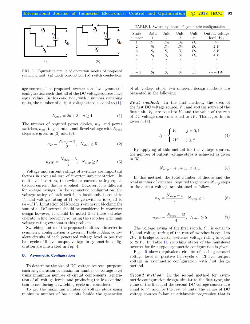
Configuration of proposed multilevel inverter is shownin Fig. 1 The proposed topology consists of series-connected basic switching units which are composed of aDC voltage source, a power transistor and a diode. Fig.2a shows the basic unit for the proposed inverter. Basicswitching units can be connected in series to increase thenumber of voltage level appears in the converter output,as shown in Fig. 2b.
Operation modes of the switching unit are shown inFig. 3. As shown in this figure, the proposed switchingunit has two operation modes. In these modes, the powerswitch and power diode operate complementary. In thefirst mode, when the power switch is off, the diode be-comes forward biased through the DC voltage source andconducts the current. In this mode, unit output voltage,Vdc, is equal to zero. In the second mode, the switch isturned on, and the diode becomes reverse biased throughthe switch and voltage source, and then turns off and theunit output voltage is equal to Vj .
Operation of the extended configuration of switching
FIG. 1. Configuration of proposed multilevel inverter.
(a)
(b)
FIG. 2. (a) Basic unit for DC voltage source switching, (b)extended configuration of basic switching unit.
unit is similar to the operation of each switching unit sothat, if a power switch does not receive any gate pulse, itscomplement diode conducts. When the power switch isturned on, its complement diode becomes reverse biasedand turns off. As a result, the DC voltage source of theunit is connected in series with the previous DC voltagesource. Therefore, it is possible to generate a multi-stepDC voltage using the mentioned extended configuration.
The output voltage of the extended configuration isalways positive. To operate as an inverter, the outputvoltage polarity should be changed in each switching cy-cle. To get this aim, a conventional H-bridge converteris added to output of the extended configuration. Con-sidering the proposed multilevel inverter structure, it isrealized that the generated multilevel voltage is providedusing less number of power switches.
III. SYMMETRIC AND ASYMMETRICCONFIGURATIONS OF PROPOSED MULTILEVELINVERTER
A. Symmetric Configuration
In design of DC voltage source size for a multilevel in-verter, it should be noted that all the voltage steps shouldbe generated in the converter output using available volt-
FIG. 3. Equivalent circuit of operation modes of proposedswitching unit: (a) diode conduction, (b) switch conduction.
age sources. The proposed inverter can have symmetricconfiguration such that all of the DC voltage sources haveequal values. In this condition, with n number switchingunits, the number of output voltage steps is equal to (1).
Nstep = 2n+ 3, n ≥ 1 (1)
The number of required power diodes, nD, and powerswitches, nsw, to generate a multilevel voltage with Nstepsteps are given in (2) and (3).
nD =Nstep − 3
2, Nstep ≥ 5 (2)
nSW =Nstep + 5
2, Nstep ≥ 5 (3)
Voltage and current ratings of switches are importantfactors in cost and size of inverter implementation. Inmultilevel inverters, the switches current rating equalsto load current that is supplied. However, it is differentfor voltage ratings. In the symmetric configuration, thevoltage rating of each switch in basic unit is equal toV , and voltage rating of H-bridge switches is equal to(n+1)V . Limitation of H-bridge switches in blocking thesum of all DC sources should be considered in converterdesign however, it should be noted that these switchesoperate in line frequency so, using the switches with highvoltage rating extenuates this problem.
Switching states of the proposed multilevel inverter insymmetric configuration is given in Table I. Also, equiv-alent circuits of each generated voltage level in positivehalf-cycle of 9-level output voltage in symmetric config-uration are illustrated in Fig. 4.
B. Asymmetric Configurations
To determine the size of DC voltage sources, purposessuch as generation of maximum number of voltage levelusing minimum number of circuit components, genera-tion of all voltage levels, and producing the less conduc-tion losses during a switching cycle are considered.
To get the maximum number of voltage steps usingminimum number of basic units beside the generation
TABLE I. Switching states of symmetric configuration
State Unit. Unit. Unit. Unit. Output voltagenumber 1 2 3 n level, Vdc
of all voltage steps, two different design methods arepresented in the following:
First method: In the first method, the sizes ofthe first DC voltage source, V0, and voltage source of thefirst unit, V1, are equal to V , and the value of the restof DC voltage sources is equal to 2V . This algorithm isgiven in (4).
Vj =
V, j = 0, 1
2V, j ≥ 2(4)
By applying of this method for the voltage sources,the number of output voltage steps is achieved as givenin (5).
Nstep = 4n+ 1, n ≥ 1 (5)
In this method, the total number of diodes and thetotal number of switches, required to generate Nstep stepsin the output voltage, are obtained as follow.
nD =Nstep − 1
4, Nstep ≥ 5 (6)
nSW =Nstep + 15
4, Nstep ≥ 5 (7)
The voltage rating of the first switch, S1, is equal toV , and voltage rating of the rest of switches is equal to2V . H-bridge converter switches voltage rating is equalto 2nV . In Table II, switching states of the multilevelinverter for first type asymmetric configuration is given.
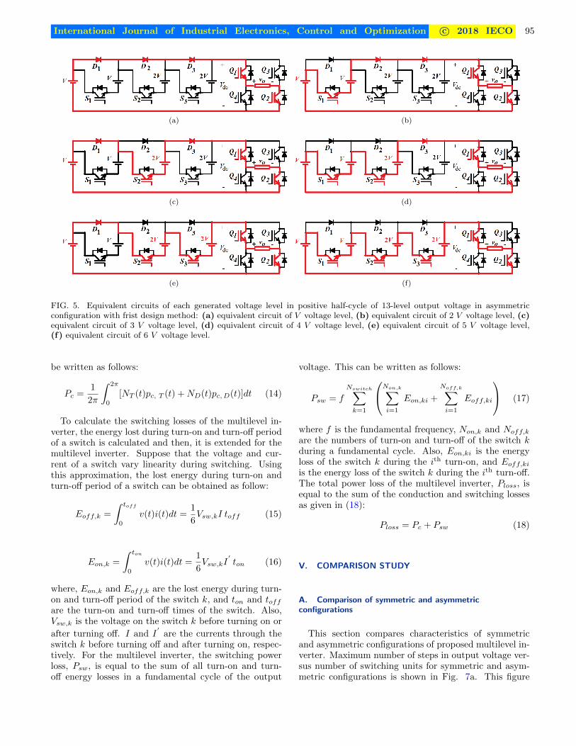
Fig. 5 shows equivalent circuits of each generatedvoltage level in positive half-cycle of 13-level outputvoltage in asymmetric configuration with first designmethod.
Second method: In the second method for asym-metric configuration design, similar to the first type, thevalue of the first and the second DC voltage sources areequal to V , and for the rest of units, the values of DCvoltage sources follow an arithmetic progression that is
FIG. 4. Equivalent circuits of each generated voltage level in positive half-cycle of 9-level output voltage in symmetric configu-ration: (a) equivalent circuit of V voltage level, (b) equivalent circuit of 2 V voltage level, (c) equivalent circuit of 3 V voltagelevel, (d) equivalent circuit of 4 V voltage level.
given in (8).
Vj =
V, j = 0, 1
2(j − 1)V, j ≥ 2(8)
By applying of this method for sizing of DC voltagesources, the number of output voltage steps is equal to(9).
Nstep = 2n2 − 2n+ 5 , n ≥ 2 (9)
and the total number of diodes and switches, required toproduce Nstep steps in the output voltage are calculatedusing (10) and (11).
nD =1 +
√2Nstep − 9
2, Nstep ≥ 5 (10)
nSW =9 +
√2Nstep − 9
2, Nstep ≥ 5 (11)
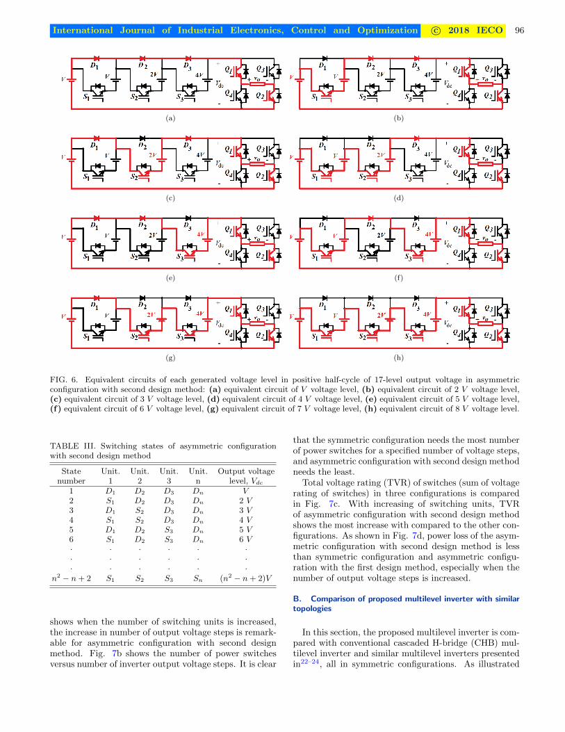
Similar to the previous method, the voltage rating ofthe first switch is equal to V , and voltage rating of switchin jth unit is equal to 2(j− 1)V . Also, the voltage ratingof H-bridge switches is equal to (n2−n+2)V . Switchingstates of asymmetric configuration in the second methodare given in Table III. In Fig. 6, equivalent circuits ofeach generated voltage level in positive half-cycle of 17-level output voltage with second design method are illus-trated.
IV. POWER LOSS CALCULATION
Power losses of the switches in a multilevel invertermainly include conduction loss and switching loss. Inthe low switching frequencies, the conduction losses aredominant. However, in the high switching frequencies,
TABLE II. Switching states of asymmetric configuration withfirst design method
State Unit. Unit. Unit. Unit. Output voltagenumber 1 2 3 n level, Vdc
the switching losses become considerable. For a transis-tor with the anti-parallel diode, both the transistor andthe diode have on-state resistance and on-state voltagewhich cause conduction losses. Although, their varia-tion with temperature is considered constant to simplifyanalysis. Assume that the on-state voltages of the diodeand transistor are VT and VD, respectively and their re-sistances are considered to be RT and RD, respectively.Instantaneous conduction loss of a diode, Pc,D(t), and atransistor, Pc,T (t), can be written as follow21:
pc, T (t) = [VT +RT iβ(t)]i(t) (12)
pc,D(t) = [VD +RDi(t)]i(t) (13)
where β is constant of the transistor, i(t) is the instanta-neous current through the transistor or diode. Consider-ing that at the instant of t, there are NT transistors andND diodes in the current path, the average value of theconduction power loss, Pc, of the multilevel inverter can
FIG. 5. Equivalent circuits of each generated voltage level in positive half-cycle of 13-level output voltage in asymmetricconfiguration with frist design method: (a) equivalent circuit of V voltage level, (b) equivalent circuit of 2 V voltage level, (c)equivalent circuit of 3 V voltage level, (d) equivalent circuit of 4 V voltage level, (e) equivalent circuit of 5 V voltage level,(f) equivalent circuit of 6 V voltage level.
be written as follows:
Pc =1
2π
∫ 2π
0
[NT (t)pc, T (t) +ND(t)pc,D(t)]dt (14)
To calculate the switching losses of the multilevel in-verter, the energy lost during turn-on and turn-off periodof a switch is calculated and then, it is extended for themultilevel inverter. Suppose that the voltage and cur-rent of a switch vary linearity during switching. Usingthis approximation, the lost energy during turn-on andturn-off period of a switch can be obtained as follow:
Eoff,k =
∫ toff
0
v(t)i(t)dt =1
6Vsw,kI toff (15)
Eon,k =
∫ ton
0
v(t)i(t)dt =1
6Vsw,kI
′ton (16)
where, Eon,k and Eoff,k are the lost energy during turn-on and turn-off period of the switch k, and ton and toffare the turn-on and turn-off times of the switch. Also,Vsw,k is the voltage on the switch k before turning on or
after turning off. I and I′
are the currents through theswitch k before turning off and after turning on, respec-tively. For the multilevel inverter, the switching powerloss, Psw, is equal to the sum of all turn-on and turn-off energy losses in a fundamental cycle of the output
voltage. This can be written as follows:
Psw = f
Nswitch∑k=1
Non,k∑i=1
Eon,ki +
Noff,k∑i=1
Eoff,ki
(17)
where f is the fundamental frequency, Non,k and Noff,kare the numbers of turn-on and turn-off of the switch kduring a fundamental cycle. Also, Eon,ki is the energyloss of the switch k during the ith turn-on, and Eoff,kiis the energy loss of the switch k during the ith turn-off.The total power loss of the multilevel inverter, Ploss, isequal to the sum of the conduction and switching lossesas given in (18):
Ploss = Pc + Psw (18)
V. COMPARISON STUDY
A. Comparison of symmetric and asymmetricconfigurations
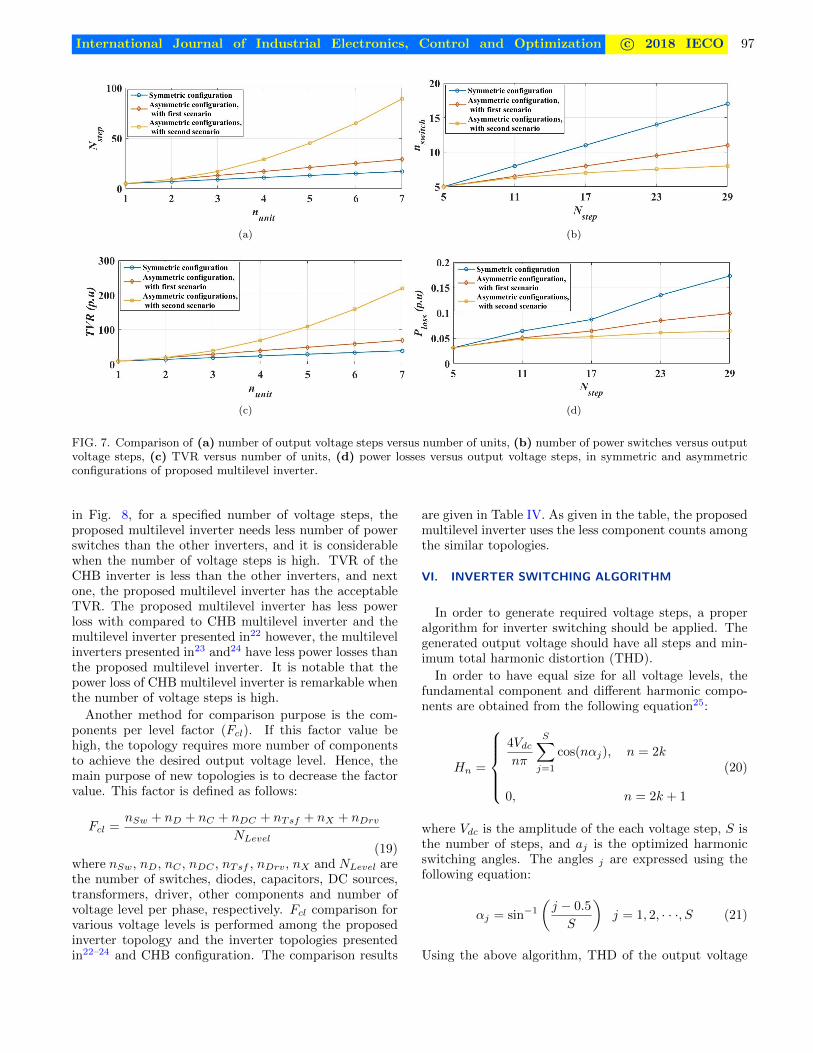
This section compares characteristics of symmetricand asymmetric configurations of proposed multilevel in-verter. Maximum number of steps in output voltage ver-sus number of switching units for symmetric and asym-metric configurations is shown in Fig. 7a. This figure
FIG. 6. Equivalent circuits of each generated voltage level in positive half-cycle of 17-level output voltage in asymmetricconfiguration with second design method: (a) equivalent circuit of V voltage level, (b) equivalent circuit of 2 V voltage level,(c) equivalent circuit of 3 V voltage level, (d) equivalent circuit of 4 V voltage level, (e) equivalent circuit of 5 V voltage level,(f) equivalent circuit of 6 V voltage level, (g) equivalent circuit of 7 V voltage level, (h) equivalent circuit of 8 V voltage level.
TABLE III. Switching states of asymmetric configurationwith second design method
State Unit. Unit. Unit. Unit. Output voltagenumber 1 2 3 n level, Vdc
shows when the number of switching units is increased,the increase in number of output voltage steps is remark-able for asymmetric configuration with second designmethod. Fig. 7b shows the number of power switchesversus number of inverter output voltage steps. It is clear
that the symmetric configuration needs the most numberof power switches for a specified number of voltage steps,and asymmetric configuration with second design methodneeds the least.
Total voltage rating (TVR) of switches (sum of voltagerating of switches) in three configurations is comparedin Fig. 7c. With increasing of switching units, TVRof asymmetric configuration with second design methodshows the most increase with compared to the other con-figurations. As shown in Fig. 7d, power loss of the asym-metric configuration with second design method is lessthan symmetric configuration and asymmetric configu-ration with the first design method, especially when thenumber of output voltage steps is increased.
B. Comparison of proposed multilevel inverter with similartopologies
In this section, the proposed multilevel inverter is com-pared with conventional cascaded H-bridge (CHB) mul-tilevel inverter and similar multilevel inverters presentedin22–24, all in symmetric configurations. As illustrated
FIG. 7. Comparison of (a) number of output voltage steps versus number of units, (b) number of power switches versus outputvoltage steps, (c) TVR versus number of units, (d) power losses versus output voltage steps, in symmetric and asymmetricconfigurations of proposed multilevel inverter.
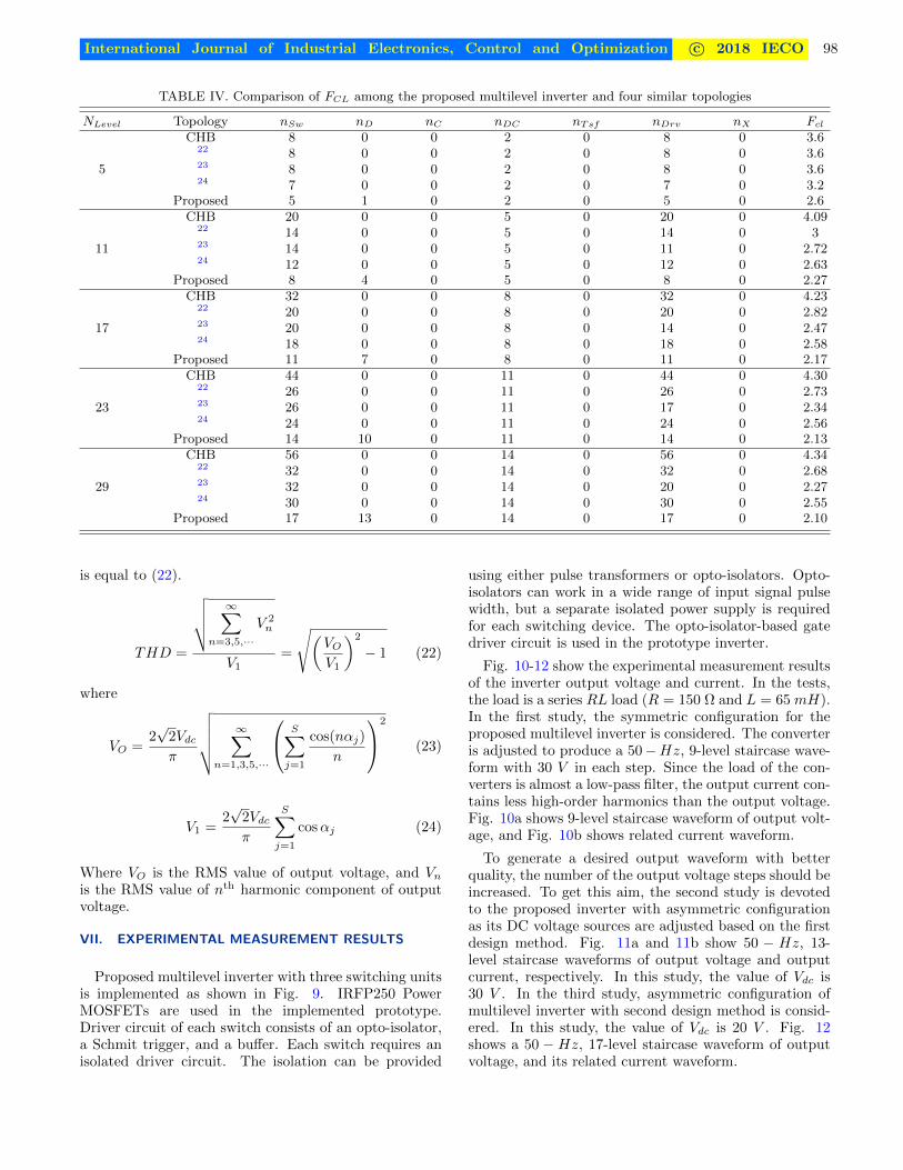
in Fig. 8, for a specified number of voltage steps, theproposed multilevel inverter needs less number of powerswitches than the other inverters, and it is considerablewhen the number of voltage steps is high. TVR of theCHB inverter is less than the other inverters, and nextone, the proposed multilevel inverter has the acceptableTVR. The proposed multilevel inverter has less powerloss with compared to CHB multilevel inverter and themultilevel inverter presented in22 however, the multilevelinverters presented in23 and24 have less power losses thanthe proposed multilevel inverter. It is notable that thepower loss of CHB multilevel inverter is remarkable whenthe number of voltage steps is high.
Another method for comparison purpose is the com-ponents per level factor (Fcl). If this factor value behigh, the topology requires more number of componentsto achieve the desired output voltage level. Hence, themain purpose of new topologies is to decrease the factorvalue. This factor is defined as follows:
Fcl =nSw + nD + nC + nDC + nTsf + nX + nDrv
NLevel(19)
where nSw, nD, nC , nDC , nTsf , nDrv, nX and NLevel arethe number of switches, diodes, capacitors, DC sources,transformers, driver, other components and number ofvoltage level per phase, respectively. Fcl comparison forvarious voltage levels is performed among the proposedinverter topology and the inverter topologies presentedin22–24 and CHB configuration. The comparison results
are given in Table IV. As given in the table, the proposedmultilevel inverter uses the less component counts amongthe similar topologies.
VI. INVERTER SWITCHING ALGORITHM
In order to generate required voltage steps, a properalgorithm for inverter switching should be applied. Thegenerated output voltage should have all steps and min-imum total harmonic distortion (THD).
In order to have equal size for all voltage levels, thefundamental component and different harmonic compo-nents are obtained from the following equation25:
Hn =
4Vdcnπ
S∑j=1
cos(nαj), n = 2k
0, n = 2k + 1
(20)
where Vdc is the amplitude of the each voltage step, S isthe number of steps, and aj is the optimized harmonicswitching angles. The angles j are expressed using thefollowing equation:
αj = sin−1(j − 0.5
S
)j = 1, 2, · · ·, S (21)
Using the above algorithm, THD of the output voltage
Where VO is the RMS value of output voltage, and Vnis the RMS value of nth harmonic component of outputvoltage.
VII. EXPERIMENTAL MEASUREMENT RESULTS
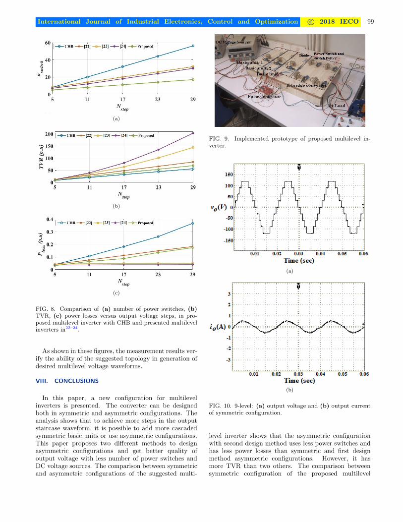
Proposed multilevel inverter with three switching unitsis implemented as shown in Fig. 9. IRFP250 PowerMOSFETs are used in the implemented prototype.Driver circuit of each switch consists of an opto-isolator,a Schmit trigger, and a buffer. Each switch requires anisolated driver circuit. The isolation can be provided
using either pulse transformers or opto-isolators. Opto-isolators can work in a wide range of input signal pulsewidth, but a separate isolated power supply is requiredfor each switching device. The opto-isolator-based gatedriver circuit is used in the prototype inverter.
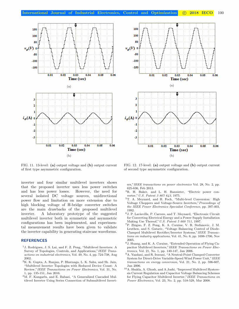
Fig. 10-12 show the experimental measurement resultsof the inverter output voltage and current. In the tests,the load is a series RL load (R = 150 Ω and L = 65 mH).In the first study, the symmetric configuration for theproposed multilevel inverter is considered. The converteris adjusted to produce a 50−Hz, 9-level staircase wave-form with 30 V in each step. Since the load of the con-verters is almost a low-pass filter, the output current con-tains less high-order harmonics than the output voltage.Fig. 10a shows 9-level staircase waveform of output volt-age, and Fig. 10b shows related current waveform.
To generate a desired output waveform with betterquality, the number of the output voltage steps should beincreased. To get this aim, the second study is devotedto the proposed inverter with asymmetric configurationas its DC voltage sources are adjusted based on the firstdesign method. Fig. 11a and 11b show 50 − Hz, 13-level staircase waveforms of output voltage and outputcurrent, respectively. In this study, the value of Vdc is30 V . In the third study, asymmetric configuration ofmultilevel inverter with second design method is consid-ered. In this study, the value of Vdc is 20 V . Fig. 12shows a 50 − Hz, 17-level staircase waveform of outputvoltage, and its related current waveform.
FIG. 8. Comparison of (a) number of power switches, (b)TVR, (c) power losses versus output voltage steps, in pro-posed multilevel inverter with CHB and presented multilevelinverters in22–24.
As shown in these figures, the measurement results ver-ify the ability of the suggested topology in generation ofdesired multilevel voltage waveforms.
VIII. CONCLUSIONS
In this paper, a new configuration for multilevelinverters is presented. The converter can be designedboth in symmetric and asymmetric configurations. Theanalysis shows that to achieve more steps in the outputstaircase waveform, it is possible to add more cascadedsymmetric basic units or use asymmetric configurations.This paper proposes two different methods to designasymmetric configurations and get better quality ofoutput voltage with less number of power switches andDC voltage sources. The comparison between symmetricand asymmetric configurations of the suggested multi-
FIG. 9. Implemented prototype of proposed multilevel in-verter.
(a)
(b)
FIG. 10. 9-level: (a) output voltage and (b) output currentof symmetric configuration.
level inverter shows that the asymmetric configurationwith second design method uses less power switches andhas less power losses than symmetric and first designmethod asymmetric configurations. However, it hasmore TVR than two others. The comparison betweensymmetric configuration of the proposed multilevel
FIG. 11. 13-level: (a) output voltage and (b) output currentof first type asymmetric configuration.
inverter and four similar multilevel inverters showsthat the proposed inverter uses less power switchesand has less power losses. However, the need forseveral isolated DC voltage sources, unidirectionalpower flow and limitation on more extension due tohigh blocking voltage of H-bridge converter switchesare the main drawbacks of the proposed multilevelinverter. A laboratory prototype of the suggestedmultilevel inverter both in symmetric and asymmetricconfigurations has been implemented, and experimen-tal measurement results have been given to validatethe inverter capability in generating staircase waveforms.
REFERENCES
1J. Rodriguez, J. S. Lai, and F. Z. Peng, “Multilevel Inverters: ASurvey of Topologies, Controls, and Applications,”IEEE Trans-actions on industrial electronics, Vol. 49, No. 4, pp. 724-738, Aug2002.
2K. K. Gupta, A. Ranjan, P. Bhatnaga, L. K. Sahu, and Sh. Jain,“Multilevel Inverter Topologies with Reduced Device Count: AReview,”IEEE Transactions on Power Electronics, Vol. 31, No.1, pp. 135-151, Jan 2016.
3M. F. Kangarlu, and E. Babaei, “A Generalized Cascaded Mul-tilevel Inverter Using Series Connection of Submultilevel Invert-
(a)
(b)
FIG. 12. 17-level: (a) output voltage and (b) output currentof second type asymmetric configuration.
ers,”IEEE transactions on power electronics Vol. 28, No. 2, pp.625-636, Feb 2013.
4R. H. Baker, and L. H. Bannister, “Electric power con-verter,”U.S. Patent 3 867 643, 1975.
5T. A. Meynard, and H. Foch, “Multi-level Conversion: HighVoltage Choppers and Voltage-Source Inverters,”Proceedings ofthe IEEE Power Electronics Specialist Conference, pp. 397-403,1992.
6J. P. Lavieville, P. Carrere, and T. Meynard, “Electronic Circuitfor Converting Electrical Energy and a Power Supply InstallationMaking Use Thereof,”U.S. Patent 5 668 711, 1997.
7P. Zhiguo, F. Z. Peng, K. A. Corzine, V. R. Stefanovic, J. M.Leuthen, and S. Gataric, “Voltage Balancing Control of Diode-Clamped Multilevel Rectifier/Inverter Systems,”IEEE Transac-tions on industry applications, Vol. 41, No. 6, pp. 1698-1706, Nov2005.
8J. Huang, and K. A. Corzine, “Extended Operation of Flying Ca-pacitor Multilevel Inverters,”IEEE Transactions on Power Elec-tronics, Vol. 21, No. 1, pp. 140-147, Jan 2006.
9A. Yazdani, and R. Iravani, “A Neutral-Point Clamped ConverterSystem for Direct-Drive Variable-Speed Wind Power Unit,”IEEEtransactions on energy conversion, Vol. 21, No. 2, pp. 596-607,Jun 2006.
10A. Shukla, A. Ghosh, and A.Joshi, “Improved Multilevel Hystere-sis Current Regulation and Capacitor Voltage Balancing Schemesfor Flying Capacitor Multilevel Inverter,”IEEE Transactions onPower Electronics, Vol. 23, No. 2, pp. 518-529, Mar 2008.
11H. Akagi, and T. Hatada, “Voltage Balancing Control for aThree-Level Diode-Clamped Converter in a Medium-VoltageTransformerless Hybrid Active Filter,”IEEE Transactions onPower Electronics, Vol. 24, No. 3, pp. 571-579, Mar 2009.
12M. Khazraei, H. Sepahvand, K. A. Corzine, and M. Ferdowsi,“Active Capacitor Voltage Balancing in Single-Phase Flying-Capacitor Multilevel Power Converters,”IEEE Transactions onIndustrial Electronics, Vol. 59, No. 2, pp. 769-778, Feb 2012.
13G. Grandi, D. Ostojic, C.Rossi, and A. Lega, “Control Strat-egy for a Multilevel Inverter in Grid-Connected Photovoltaic Ap-plications,”Electrical Machines and Power Electronics, ACEMP’07. International Aegean Conference on, pp.156-161, 2007.
14P. Lezana, J. Rodriguez, and D. A. Oyarzun, “Cascaded Multi-level Inverter with Regeneration Capability and Reduced Num-ber of Switches,”IEEE Transactions on Industrial Electronics,Vol. 55, No. 3, pp. 1059-1066, March 2008.
15Z. Du, B. Ozpineci, L. M. Tolbert, and J. N. Chiasson, “DC-ACCascaded H-Bridge Multilevel Boost Inverter With No Inductorsfor Electric/Hybrid Electric Vehicle Applications,”IEEE Trans-actions on Industry Applications, Vol. 45, No. 3, pp. 963-970,May 2009.
16S. Debnath, J. Qin, B. Bahrani, M. Saeedifard and P. Barbosa,“Operation, Control, and Applications of the Modular MultilevelConverter: A Review,”IEEE Transactions on Power Electronics,Vol. 30, No. 1, pp. 37-53, Jan 2015.
17Ch. I. Odeh, E. S. Obe, and O. Ojo, “Topology for CascadedMultilevel Inverter,”IET Power Electronics, Vol. 9, NO. 5, pp.921-929, Apr 2016.
18R. Barzegarkhoo, E. Zamiri, N. Vosoughi, H. M. Kojabadi, and L.Chang, “Cascaded Multilevel Inverter Using Series Connection ofNovel Capacitor-based Units with Minimum Switch Count,”IETPower Electronics, Vol. 9, NO. 10, pp. 2060-2075, Aug 2016.
19R. R. Karasani, V. B. Borghate, P. M. Meshram, H. M.Suryawanshi, and S. Sabyasachi, “A Three-Phase Hybrid Cas-caded Modular Multilevel Inverter for Renewable Energy Envi-ronment,”IEEE Transactions on Power Electronics, Vol. 32, No.2, pp. 1070-1087, Feb 2017.
20N. Prabaharan, and K. Palanisamy, “Analysis of Cascaded H-Bridge Multilevel Inverter Configuration with Double Level Cir-cuit,”IET Power Electronics, Vol. 10, No. 9, pp. 1023-1033, Jul2017.
21E. Babaei, S. Alilu, and S. Laali, “A New General Topology forCascaded Multilevel Inverters with Reduced Number of Com-ponents Based on Developed H-bridge,”IEEE Transactions onIndustrial Electronics, Vol. 61, No. 8, pp. 3932-3939, Aug 2014.
22E. Babaei, and S. H Hosseini, “New Cascaded Multilevel InverterTopology with Minimum Number of Switches,”Energy Conver-sion and Management, Vol. 50, No. 11, pp. 2761-2767, Nov 2009.
23M. Farhadi Kangarlu and E. Babaei, “A Generalized CascadedMultilevel Inverter Using Series Connection of Sub-Multilevel In-verters,”IEEE transactions on power electronics, Vol. 28, No. 2,pp. 625-636, Feb 2013.
24H. Samsami, A. Taheri, and R. Samanbakhsh, “New Bidirec-tional Multilevel Inverter Topology with Staircase Cascading forSymmetric and Asymmetric Structures,”IET Power Electronics,Vol. 10, No. 11, pp. 1315-1323, Nov 2017.
25E. Babaei, S. H. Hosseini, G. B. Gharehpetian, M. T. Haque,and M. Sabahi, “Reduction of DC Voltage Sources and Switchesin Asymmetrical Multilevel Converters Using a Novel Topol-ogy,”Electric Power Systems Research, Vol. 77, No. 8, pp. 1073-1085, Jun 2007.
Farzad Sedaghati was bornin Ardabil, Iran, in 1984. Hereceived the M.S. and Ph.Ddegrees both in electrical en-gineering in 2010 and 2014from the University of Tabriz,Tabriz, Iran. In 2014, he joinedthe Faculty of Engineering, Mo-haghegh Ardabili, where hehas been an Assistant Profes-sor since 2014. His current re-search interests include power
electronic converters design and applications.
Seyed Naser Hashemipourwas born in Kermanshah, Iran,in 1991. He received the B.Sc.degree in electrical engineeringfrom University of MohagheghArdabili, Ardabil, Iran, in 2015.Currently, he is M.S. studentof Power Systems in ShirazUniversity of Technology, Shi-raz, Iran. His research inter-ests include distribution systemanalysis, energy management,