SN54ALS569A, SN74ALS568A, SN74ALS569A SYNCHRONOUS 4-BIT UP/DOWN DECADE AND BINARY COUNTERS WITH 3-STATE OUTPUTS SDAS229A – APRIL 1982 – REVISED JANUARY 1995 Copyright 1995, Texas Instruments Incorporated 1 POST OFFICE BOX 655303 • DALLAS, TEXAS 75265 • 3-State Q Outputs Drive Bus Lines Directly • Counter Operation Independent of 3-State Output • Fully Synchronous Clear, Count, and Load • Asynchronous Clear Is Also Provided • Fully Cascadable • Package Options Include Plastic Small-Outline (DW) Packages, Ceramic Chip Carriers (FK), and Standard Plastic (N) and Ceramic (J) 300-mil DIPs description The SN74ALS568A decade counter and ′ALS569A binary counters are programmable, count up or down, and offer both synchronous and asynchronous clearing. All synchronous functions are executed on the positive-going edge of the clock (CLK) input. The clear function is initiated by applying a low level to either asynchronous clear (ACLR ) or synchronous clear (SCLR ). Asynchronous (direct) clearing overrides all other functions of the device, while synchronous clearing overrides only the other synchronous functions. Data is loaded from the A, B, C, and D inputs by holding load (LOAD ) low during a positive-going clock transition. The counting function is enabled only when enable P (ENP ) and enable T (ENT ) are low and ACLR , SCLR , and LOAD are high. The up/down (U/D ) input controls the direction of the count. These counters count up when U/D is high and count down when U/D is low. A high level at the output-enable (OE ) input forces the Q outputs into the high-impedance state, and a low level enables those outputs. Counting is independent of OE . ENT is fed forward to enable the ripple-carry output (RCO ) to produce a low-level pulse while the count is zero (all Q outputs low) when counting down or maximum (9 or 15) when counting up. The clocked carry output (CCO ) produces a low-level pulse for a duration equal to that of the low level of the clock when RCO is low and the counter is enabled (both ENP and ENT are low); otherwise, CCO is high. CCO does not have the glitches commonly associated with a ripple-carry output. Cascading is normally accomplished by connecting RCO or CCO of the first counter to ENT of the next counter. However, for very high-speed counting, RCO should be used for cascading since CCO does not become active until the clock returns to the low level. The SN54ALS569A is characterized for operation over the full military temperature range of – 55°C to 125°C. The SN74ALS568A and SN74ALS569A are characterized for operation from 0°C to 70°C. 1 2 3 4 5 6 7 8 9 10 20 19 18 17 16 15 14 13 12 11 U/D CLK A B C D ENP ACLR SCLR GND V CC RCO CCO OE Q A Q B Q C Q D ENT LOAD SN54ALS569A . . . J PACKAGE SN74ALS568A, SN74ALS569A . . . DW OR N PACKAGE (TOP VIEW) 3 2 1 20 19 9 10 11 12 13 4 5 6 7 8 18 17 16 15 14 CCO OE Q A Q B Q C B C D ENP ACLR SN54ALS569A . . . FK PACKAGE (TOP VIEW) A CLK U/D ENT Q RCO SCLR GND LOAD V CC D PRODUCTION DATA information is current as of publication date. Products conform to specifications per the terms of Texas Instruments standard warranty. Production processing does not necessarily include testing of all parameters.
Transcript
SN54ALS569A, SN74ALS568A, SN74ALS569A SYNCHRONOUS 4-BIT UP/DOWN DECADE AND BINARY COUNTERS
WITH 3-STATE OUTPUTS SDAS229A – APRIL 1982 – REVISED JANUARY 1995
Copyright 1995, Texas Instruments Incorporated
1POST OFFICE BOX 655303 • DALLAS, TEXAS 75265
• 3-State Q Outputs Drive Bus Lines Directly
• Counter Operation Independent of 3-StateOutput
• Fully Synchronous Clear, Count, and Load
• Asynchronous Clear Is Also Provided
• Fully Cascadable
• Package Options Include PlasticSmall-Outline (DW) Packages, CeramicChip Carriers (FK), and Standard Plastic (N)and Ceramic (J) 300-mil DIPs
description
The SN74ALS568A decade counter and′ALS569A binary counters are programmable,count up or down, and offer both synchronous andasynchronous clearing. All synchronous functionsare executed on the positive-going edge of theclock (CLK) input.
The clear function is initiated by applying a lowlevel to either asynchronous clear (ACLR) orsynchronous clear (SCLR). Asynchronous (direct)clearing overrides all other functions of the device,while synchronous clearing overrides only theother synchronous functions. Data is loaded fromthe A, B, C, and D inputs by holding load (LOAD)low during a positive-going clock transition. Thecounting function is enabled only when enable P(ENP) and enable T (ENT) are low and ACLR,SCLR, and LOAD are high. The up/down (U/D)input controls the direction of the count. Thesecounters count up when U/D is high and countdown when U/D is low.
A high level at the output-enable (OE) input forces the Q outputs into the high-impedance state, and a low levelenables those outputs. Counting is independent of OE. ENT is fed forward to enable the ripple-carry output(RCO) to produce a low-level pulse while the count is zero (all Q outputs low) when counting down or maximum(9 or 15) when counting up. The clocked carry output (CCO) produces a low-level pulse for a duration equal tothat of the low level of the clock when RCO is low and the counter is enabled (both ENP and ENT are low);otherwise, CCO is high. CCO does not have the glitches commonly associated with a ripple-carry output.Cascading is normally accomplished by connecting RCO or CCO of the first counter to ENT of the next counter.However, for very high-speed counting, RCO should be used for cascading since CCO does not become activeuntil the clock returns to the low level.
The SN54ALS569A is characterized for operation over the full military temperature range of –55°C to 125°C.The SN74ALS568A and SN74ALS569A are characterized for operation from 0°C to 70°C.
1
2
3
4
5
6
7
8
9
10
20
19
18
17
16
15
14
13
12
11
U/DCLK
ABCD
ENPACLRSCLRGND
VCCRCOCCOOEQAQBQCQDENTLOAD
SN54ALS569A . . . J PACKAGESN74ALS568A, SN74ALS569A . . . DW OR N PACKAGE
(TOP VIEW)
3 2 1 20 19
9 10 11 12 13
4
5
6
7
8
18
17
16
15
14
CCOOEQAQBQC
BCD
ENPACLR
SN54ALS569A . . . FK PACKAGE(TOP VIEW)
A CLK
U/D
EN
TQ
RC
O
SC
LRG
ND
LOA
DV C
C
D
PRODUCTION DATA information is current as of publication date.Products conform to specifications per the terms of Texas Instrumentsstandard warranty. Production processing does not necessarily includetesting of all parameters.
SN54ALS569A, SN74ALS568A, SN74ALS569ASYNCHRONOUS 4-BIT UP/DOWN DECADE AND BINARY COUNTERSWITH 3-STATE OUTPUTSSDAS229A – APRIL 1982 – REVISED JANUARY 1995
2 POST OFFICE BOX 655303 • DALLAS, TEXAS 75265
FUNCTION TABLE
INPUTSOPERATION
OE ACLR SCLR LOAD ENT ENP U/D CLKOPERATION
H X X X X X X X Q outputs disabled
L L X X X X X X Asynchronous clear
L H L X X X X ↑ Synchronous clear
L H H L X X X ↑ Load
L H H H L L H ↑ Count up
L H H H L L L ↑ Count down
L H H H H X X X Inhibit count
L H H H X H X X Inhibit count
SN54ALS569A, SN74ALS568A, SN74ALS569A SYNCHRONOUS 4-BIT UP/DOWN DECADE AND BINARY COUNTERS
WITH 3-STATE OUTPUTS SDAS229A – APRIL 1982 – REVISED JANUARY 1995
3POST OFFICE BOX 655303 • DALLAS, TEXAS 75265
logic symbols †
ENP
CTRDIV10
LOAD
3,5D3
A4
B5
C6
D
C5/1,4,7,8,+/2,4,7,8–
191,7 (CT=9) G9
10 QA
QB
QC
QD
U/D
ENT RCO
2,7 (CT=0) G9
186,7,8,9 CCO
EN1017
M2 [DOWN]
M1 [UP]1
Z6
2CLK
G712
G87
5CT=09
M4 [COUNT]
M3 [LOAD]11
CT=08
OE
SCLR
ACLR
16
15
14
13
SN74ALS568A
ENP
CTRDIV16
LOAD
3,5D3
A4
B5
C6
D
C5/1,4,7,8,+/2,4,7,8–
191,7 (CT=15) G9
10 QA
QB
QCQD
U/D
ENT RCO
2,7 (CT=0) G9
186,7,8,9 CCO
EN1017
M2 [DOWN]
M1 [UP]1
Z6
2CLK
G712
G87
5CT=09
M4 [COUNT]
M3 [LOAD]11
CT=08
OE
SCLR
ACLR
16
15
14
13
′ALS569A
† These symbols are in accordance with ANSI/IEEE Std 91-1984 and IEC Publication 617-12.
SN54ALS569A, SN74ALS568A, SN74ALS569ASYNCHRONOUS 4-BIT UP/DOWN DECADE AND BINARY COUNTERSWITH 3-STATE OUTPUTSSDAS229A – APRIL 1982 – REVISED JANUARY 1995
4 POST OFFICE BOX 655303 • DALLAS, TEXAS 75265
logic diagrams (positive logic)
C11DR
C11DR
C11DR
C11DR
17
1
2
12
9
11
8
3
4
5
6
7
18
19
16
15
14
13
CCO
RCO
QA
QB
QC
QD
OE
U/D
CLK
ENT
ENP
SCLR
LOAD
ACLR
A
B
C
D
SN74ALS568A
SN54ALS569A, SN74ALS568A, SN74ALS569A SYNCHRONOUS 4-BIT UP/DOWN DECADE AND BINARY COUNTERS
WITH 3-STATE OUTPUTS SDAS229A – APRIL 1982 – REVISED JANUARY 1995
5POST OFFICE BOX 655303 • DALLAS, TEXAS 75265
logic diagrams (positive logic) (continued)
C11DR
C11DR
C11DR
C11DR
17
1
2
12
9
11
8
3
4
5
6
7
18
19
16
15
14
13
CCO
RCO
QA
QB
QC
QD
OE
U/D
CLK
ENT
ENP
SCLR
LOAD
ACLR
A
B
C
D
′ALS569A
SN54ALS569A, SN74ALS568A, SN74ALS569ASYNCHRONOUS 4-BIT UP/DOWN DECADE AND BINARY COUNTERSWITH 3-STATE OUTPUTSSDAS229A – APRIL 1982 – REVISED JANUARY 1995
6 POST OFFICE BOX 655303 • DALLAS, TEXAS 75265
typical load, count, and inhibit sequences
ÌÌÌÌÌÌÌÌÌÌÌÌ
ÌÌÌÌÌÌÌÌ
Hi Z
ÌÌÌÌ
ÌÌÌÌÌÌÌÌÌÌÌÌ
ÌÌÌÌÌÌÌÌÌÌÌÌÌÌÌÌÌÌÌÌÌÌÌÌÌÌÌÌÌÌÌÌÌÌÌÌÌÌÌÌÌÌÌÌÌÌ
LOAD
A
CLK
U/D
ENT
RCO
QA
QB
QC
QD
AsyncClear
1 2
Count Down
Don’t CareDon’t Care
ÌÌÌÌÌÌÌÌÌÌÌÌÌÌÌÌÌÌÌÌÌÌÌÌÌÌÌÌÌB Don’t CareDon’t Care
ÌÌÌÌÌÌÌÌÌÌÌÌÌÌÌÌÌÌÌÌÌÌÌÌÌÌÌÌÌÌÌÌÌÌÌÌÌÌÌÌÌÌÌÌÌÌ
ÌÌÌÌÌÌÌÌÌÌÌÌ
C Don’t CareDon’t Care
ÌÌÌÌÌÌÌÌÌÌÌÌÌÌÌÌÌÌÌÌÌÌÌÌÌÌÌÌÌÌÌÌÌÌÌÌÌÌÌÌÌÌÌÌÌÌ
ÌÌÌÌÌÌÌÌÌÌÌÌ
D Don’t CareDon’t Care
Don’t Care
ÌÌÌÌ
ÌÌÌÌÌÌÌÌ
Don’t Care
ENPÌÌÌÌ
ÌÌÌÌÌÌÌÌ
Don’t Care
ÌÌÌÌ
SCLRÌÌÌÌ
ACLR
OE
ÌÌÌÌÌÌÌÌ
Hi Z
ÌÌÌÌÌÌÌÌ
Hi Z
ÌÌÌÌHi Z
CCO
Count UpInhibit
Counting
CountUp
SyncClear
SyncLoad
0 7 8 9 0 1 2 3 4 3 2 1 0 9 8
SN74ALS568A
SN54ALS569A, SN74ALS568A, SN74ALS569A SYNCHRONOUS 4-BIT UP/DOWN DECADE AND BINARY COUNTERS
WITH 3-STATE OUTPUTS SDAS229A – APRIL 1982 – REVISED JANUARY 1995
7POST OFFICE BOX 655303 • DALLAS, TEXAS 75265
typical load, count, and inhibit sequences (continued)
ÌÌÌÌÌÌÌÌÌÌÌÌ
ÌÌÌÌÌÌÌÌ
Hi Z
ÌÌÌÌ
ÌÌÌÌÌÌÌÌÌÌÌÌ
ÌÌÌÌÌÌÌÌÌÌÌÌÌÌÌÌÌÌÌÌÌÌÌÌÌÌÌÌÌÌÌÌÌÌÌÌÌÌÌÌÌÌÌÌÌÌ
LOAD
A
CLK
U/D
ENT
RCO
QA
QB
QC
QD
AsyncClear
1 2
Count Down
Don’t CareDon’t Care
ÌÌÌÌÌÌÌÌÌÌÌÌÌÌÌÌÌÌÌÌÌÌÌÌÌÌÌÌÌB Don’t CareDon’t Care
ÌÌÌÌÌÌÌÌÌÌÌÌÌÌÌÌÌÌÌÌÌÌÌÌÌÌÌÌÌÌÌÌÌÌÌÌÌÌÌÌÌÌÌÌÌÌ
ÌÌÌÌÌÌÌÌÌÌÌÌ
C Don’t CareDon’t Care
ÌÌÌÌÌÌÌÌÌÌÌÌÌÌÌÌÌÌÌÌÌÌÌÌÌÌÌÌÌÌÌÌÌÌÌÌÌÌÌÌÌÌÌÌÌÌ
ÌÌÌÌÌÌÌÌÌÌÌÌ
D Don’t CareDon’t Care
Don’t Care
ÌÌÌÌ
ÌÌÌÌÌÌÌÌ
Don’t Care
ENPÌÌÌÌ
ÌÌÌÌÌÌÌÌ
Don’t Care
ÌÌÌÌ
SCLRÌÌÌÌ
ACLR
OE
ÌÌÌÌÌÌÌÌ
Hi Z
ÌÌÌÌÌÌÌÌ
Hi Z
ÌÌÌÌHi Z
CCO
Count UpInhibit
Counting
CountUp
SyncClear
SyncLoad
0 13 14 15 0 1 2 3 4 3 2 1 0 15 14
′ALS569A
SN54ALS569A, SN74ALS568A, SN74ALS569ASYNCHRONOUS 4-BIT UP/DOWN DECADE AND BINARY COUNTERSWITH 3-STATE OUTPUTSSDAS229A – APRIL 1982 – REVISED JANUARY 1995
8 POST OFFICE BOX 655303 • DALLAS, TEXAS 75265
absolute maximum ratings over operating free-air temperature range (unless otherwise noted) †
† Stresses beyond those listed under “absolute maximum ratings” may cause permanent damage to the device. These are stress ratings only, andfunctional operation of the device at these or any other conditions beyond those indicated under “recommended operating conditions” is notimplied. Exposure to absolute-maximum-rated conditions for extended periods may affect device reliability.
recommended operating conditions
SN54ALS569ASN74ALS568ASN74ALS569A UNIT
MIN NOM MAX MIN NOM MAX
VCC Supply voltage 4.5 5 5.5 4.5 5 5.5 V
VIH High-level input voltage 2 2 V
VIL Low-level input voltage 0.7 0.8 V
IOH High level output currentQ outputs –1 –2.6
mAIOH High-level output currentCCO and RCO –0.4 –0.4
mA
IOL Low level output currentQ outputs 12 24
mAIOL Low-level output currentCCO and RCO 4 8
mA
f l k Clock frequencySN74ALS568A 0 20
MHzfclock Clock frequency′ALS569A 0 22 0 30
MHz
ACLR or LOAD low 20 15
SN74ALS568ACLK high 25
tw Pulse durationSN74ALS568A
CLK low 25 ns
′ALS569ACLK high 20 16.5
′ALS569ACLK low 23 16.5
Data at A, B, C, D 25 20
ENP ENTHigh 35 30
ENP, ENTLow 25 20
SCLRLow 20 15
tsu Setup time before CLK↑SCLR
High (inactive) 35 30 ns
LOADLow 20 15
LOADHigh (inactive) 35 30
U/D 35 30
ACLR inactive 10 10
th Hold time after CLK↑ for any input 0 0 ns
TA Operating free-air temperature –55 125 0 70 °C
SN54ALS569A, SN74ALS568A, SN74ALS569A SYNCHRONOUS 4-BIT UP/DOWN DECADE AND BINARY COUNTERS
WITH 3-STATE OUTPUTS SDAS229A – APRIL 1982 – REVISED JANUARY 1995
9POST OFFICE BOX 655303 • DALLAS, TEXAS 75265
electrical characteristics over recommended operating free-air temperature range (unlessotherwise noted)
PARAMETER TEST CONDITIONSSN54ALS569A
SN74ALS568ASN74ALS569A UNIT
MIN TYP† MAX MIN TYP† MAX
VIK VCC = 4.5 V, II = –18 mA –1.5 –1.5 V
All outputs VCC = 4.5 V to 5.5 V, IOH = –0.4 mA VCC –2 VCC –2
CCO and RCO VCC = 4 5 VIOL = 4 mA 0.25 0.4 0.25 0.4
V
CCO and RCO VCC = 4.5 VIOL = 8 mA 0.35 0.5
IOZH VCC = 5.5 V, VO = 2.7 V 20 20 µA
IOZL VCC = 5.5 V, VO = 0.4 V –20 –20 µA
II VCC = 5.5 V, VI = 7 V 0.1 0.1 mA
IIH VCC = 5.5 V, VI = 2.7 V 20 20 µA
IIL VCC = 5.5 V, VI = 0.4 V –0.2 –0.2 mA
IO‡CCO and RCO
VCC = 5 5 V VO = 2 25 V–15 –70 –15 –70
mAIO‡Q outputs
VCC = 5.5 V, VO = 2.25 V–20 –112 –30 –112
mA
Outputs high 16 26 16 26
ICC VCC = 5.5 V Outputs low 20 32 20 32 mA
Outputs disabled 20 32 20 32
† All typical values are at VCC = 5 V, TA = 25°C.‡ The output conditions have been chosen to produce a current that closely approximates one half of the true short-circuit output current, IOS.
SN54ALS569A, SN74ALS568A, SN74ALS569ASYNCHRONOUS 4-BIT UP/DOWN DECADE AND BINARY COUNTERSWITH 3-STATE OUTPUTSSDAS229A – APRIL 1982 – REVISED JANUARY 1995
10 POST OFFICE BOX 655303 • DALLAS, TEXAS 75265
switching characteristics (see Figure 1)
PARAMETERFROM
(INPUT)TO
(OUTPUT)
VCC = 4.5 V to 5.5 V,CL = 50 pF,R1 = 500 Ω,R2 = 500 Ω,TA = MIN to MAX † UNIT(INPUT) (OUTPUT)
SN54ALS569ASN74ALS568ASN74ALS569A
MIN MAX MIN MAX
fSN74ALS568A 20
MHzfmax ′ALS569A 22 30MHz
tPLHCLK An Q
4 21 4 13ns
tPHLCLK Any Q
7 19 7 16ns
tPLHCLK RCO
12 37 12 28ns
tPHLCLK RCO
10 28 10 19ns
tPLHCLK CCO
5 17 5 13ns
tPHLCLK CCO
6 30 6 25ns
tPLHU/D RCO
9 31 9 23ns
tPHLU/D RCO
9 33 9 19ns
tPLHENT RCO
6 21 6 15ns
tPHLENT RCO
4 20 4 13ns
tPLHENT CCO
5 18 5 13ns
tPHLENT CCO
9 32 9 23ns
tPLHENP CCO
4 18 4 12ns
tPHLENP CCO
5 18 5 14ns
tPHL ACLR Any Q 9 25 9 20 ns
tPZHOE An Q
6 23 6 18ns
tPZLOE Any Q
6 29 6 24ns
tPHZOE Any Q
1 12 1 10ns
tPLZOE Any Q
3 29 3 13ns
† For conditions shown as MIN or MAX, use the appropriate value specified under recommended operating conditions.
SN54ALS569A, SN74ALS568A, SN74ALS569A SYNCHRONOUS 4-BIT UP/DOWN DECADE AND BINARY COUNTERS
WITH 3-STATE OUTPUTS SDAS229A – APRIL 1982 – REVISED JANUARY 1995
11POST OFFICE BOX 655303 • DALLAS, TEXAS 75265
PARAMETER MEASUREMENT INFORMATIONSERIES 54ALS/74ALS AND 54AS/74AS DEVICES
tPHZ
tPLZ
tPHLtPLH
0.3 V
tPZL
tPZH
tPLHtPHL
LOAD CIRCUITFOR 3-STATE OUTPUTS
From OutputUnder Test
Test Point
R1
S1
CL(see Note A)
7 V
1.3 V
1.3 V1.3 V
3.5 V
3.5 V
0.3 V
0.3 V
thtsu
VOLTAGE WAVEFORMSSETUP AND HOLD TIMES
TimingInput
DataInput
1.3 V 1.3 V3.5 V
3.5 V
0.3 V
0.3 V
High-LevelPulse
Low-LevelPulse
tw
VOLTAGE WAVEFORMSPULSE DURATIONS
Input
Out-of-PhaseOutput
(see Note C)
1.3 V 1.3 V
1.3 V1.3 V
1.3 V 1.3 V
1.3 V1.3 V
1.3 V
1.3 V
3.5 V
3.5 V
0.3 V
0.3 V
VOL
VOH
VOH
VOL
OutputControl
(low-levelenabling)
Waveform 1S1 Closed
(see Note B)
Waveform 2S1 Open
(see Note B)0 V
VOH
VOL
3.5 V
In-PhaseOutput
0.3 V
1.3 V 1.3 V
VOLTAGE WAVEFORMSPROPAGATION DELAY TIMES
VOLTAGE WAVEFORMSENABLE AND DISABLE TIMES, 3-STATE OUTPUTS
R2
VCC
RL
Test Point
From OutputUnder Test
CL(see Note A)
LOAD CIRCUITFOR OPEN-COLLECTOR OUTPUTS
LOAD CIRCUIT FOR BI-STATE
TOTEM-POLE OUTPUTS
From OutputUnder Test
Test Point
CL(see Note A)
RL
RL = R1 = R2
NOTES: A. CL includes probe and jig capacitance.B. Waveform 1 is for an output with internal conditions such that the output is low except when disabled by the output control.
Waveform 2 is for an output with internal conditions such that the output is high except when disabled by the output control.C. When measuring propagation delay items of 3-state outputs, switch S1 is open.D. All input pulses have the following characteristics: PRR ≤ 1 MHz, tr = tf = 2 ns, duty cycle = 50%.E. The outputs are measured one at a time with one transition per measurement.
Figure 1. Load Circuits and Voltage Waveforms
PACKAGE OPTION ADDENDUM
www.ti.com 17-Mar-2017
Addendum-Page 1
PACKAGING INFORMATION
Orderable Device Status(1)
Package Type PackageDrawing
Pins PackageQty
Eco Plan(2)
Lead/Ball Finish(6)
MSL Peak Temp(3)
Op Temp (°C) Device Marking(4/5)
Samples
83025022A ACTIVE LCCC FK 20 1 TBD POST-PLATE N / A for Pkg Type -55 to 125 83025022ASNJ54ALS569AFK
8302502RA ACTIVE CDIP J 20 1 TBD A42 N / A for Pkg Type -55 to 125 8302502RASNJ54ALS569AJ
SN54ALS569AJ ACTIVE CDIP J 20 1 TBD A42 N / A for Pkg Type -55 to 125 SN54ALS569AJ
SN74ALS569ADWR ACTIVE SOIC DW 20 2000 Green (RoHS& no Sb/Br)
CU NIPDAU Level-1-260C-UNLIM 0 to 70 ALS569A
SN74ALS569AN ACTIVE PDIP N 20 20 Pb-Free(RoHS)
CU NIPDAU N / A for Pkg Type 0 to 70 SN74ALS569AN
SN74ALS569ANE4 ACTIVE PDIP N 20 20 Pb-Free(RoHS)
CU NIPDAU N / A for Pkg Type 0 to 70 SN74ALS569AN
SNJ54ALS569AFK ACTIVE LCCC FK 20 1 TBD POST-PLATE N / A for Pkg Type -55 to 125 83025022ASNJ54ALS569AFK
SNJ54ALS569AJ ACTIVE CDIP J 20 1 TBD A42 N / A for Pkg Type -55 to 125 8302502RASNJ54ALS569AJ
(1) The marketing status values are defined as follows:ACTIVE: Product device recommended for new designs.LIFEBUY: TI has announced that the device will be discontinued, and a lifetime-buy period is in effect.NRND: Not recommended for new designs. Device is in production to support existing customers, but TI does not recommend using this part in a new design.PREVIEW: Device has been announced but is not in production. Samples may or may not be available.OBSOLETE: TI has discontinued the production of the device.
(2) Eco Plan - The planned eco-friendly classification: Pb-Free (RoHS), Pb-Free (RoHS Exempt), or Green (RoHS & no Sb/Br) - please check http://www.ti.com/productcontent for the latest availabilityinformation and additional product content details.TBD: The Pb-Free/Green conversion plan has not been defined.Pb-Free (RoHS): TI's terms "Lead-Free" or "Pb-Free" mean semiconductor products that are compatible with the current RoHS requirements for all 6 substances, including the requirement thatlead not exceed 0.1% by weight in homogeneous materials. Where designed to be soldered at high temperatures, TI Pb-Free products are suitable for use in specified lead-free processes.Pb-Free (RoHS Exempt): This component has a RoHS exemption for either 1) lead-based flip-chip solder bumps used between the die and package, or 2) lead-based die adhesive used betweenthe die and leadframe. The component is otherwise considered Pb-Free (RoHS compatible) as defined above.Green (RoHS & no Sb/Br): TI defines "Green" to mean Pb-Free (RoHS compatible), and free of Bromine (Br) and Antimony (Sb) based flame retardants (Br or Sb do not exceed 0.1% by weightin homogeneous material)
(3) MSL, Peak Temp. - The Moisture Sensitivity Level rating according to the JEDEC industry standard classifications, and peak solder temperature.
(4) There may be additional marking, which relates to the logo, the lot trace code information, or the environmental category on the device.
(5) Multiple Device Markings will be inside parentheses. Only one Device Marking contained in parentheses and separated by a "~" will appear on a device. If a line is indented then it is a continuationof the previous line and the two combined represent the entire Device Marking for that device.
(6) Lead/Ball Finish - Orderable Devices may have multiple material finish options. Finish options are separated by a vertical ruled line. Lead/Ball Finish values may wrap to two lines if the finishvalue exceeds the maximum column width.
Important Information and Disclaimer:The information provided on this page represents TI's knowledge and belief as of the date that it is provided. TI bases its knowledge and belief on informationprovided by third parties, and makes no representation or warranty as to the accuracy of such information. Efforts are underway to better integrate information from third parties. TI has taken andcontinues to take reasonable steps to provide representative and accurate information but may not have conducted destructive testing or chemical analysis on incoming materials and chemicals.TI and TI suppliers consider certain information to be proprietary, and thus CAS numbers and other limited information may not be available for release.
In no event shall TI's liability arising out of such information exceed the total purchase price of the TI part(s) at issue in this document sold by TI to Customer on an annual basis.
OTHER QUALIFIED VERSIONS OF SN54ALS569A, SN74ALS569A :
• Catalog: SN74ALS569A
• Military: SN54ALS569A
NOTE: Qualified Version Definitions:
• Catalog - TI's standard catalog product
• Military - QML certified for Military and Defense Applications
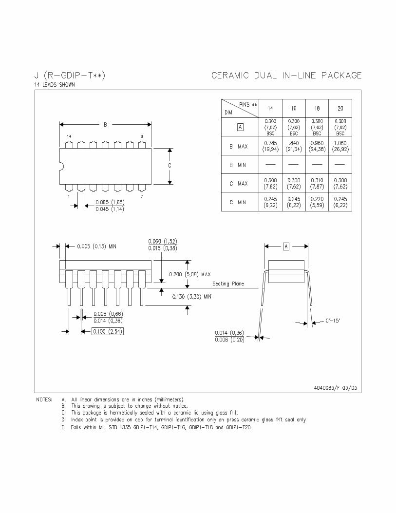
NOTES: 1. All linear dimensions are in millimeters. Dimensions in parenthesis are for reference only. Dimensioning and tolerancing per ASME Y14.5M. 2. This drawing is subject to change without notice. 3. This dimension does not include mold flash, protrusions, or gate burrs. Mold flash, protrusions, or gate burrs shall not exceed 0.15 mm per side. 4. This dimension does not include interlead flash. Interlead flash shall not exceed 0.43 mm per side.5. Reference JEDEC registration MS-013.
120
0.25 C A B
1110
PIN 1 IDAREA
NOTE 4
SEATING PLANE
0.1 C
SEE DETAIL A
DETAIL ATYPICAL
SCALE 1.200
www.ti.com
EXAMPLE BOARD LAYOUT
(9.3)
0.07 MAXALL AROUND
0.07 MINALL AROUND
20X (2)
20X (0.6)
18X (1.27)
(R )TYP
0.05
4220724/A 05/2016
SOIC - 2.65 mm max heightDW0020ASOIC
SYMM
SYMM
LAND PATTERN EXAMPLESCALE:6X
1
10 11
20
NOTES: (continued) 6. Publication IPC-7351 may have alternate designs. 7. Solder mask tolerances between and around signal pads can vary based on board fabrication site.
METALSOLDER MASKOPENING
NON SOLDER MASKDEFINED
SOLDER MASK DETAILS
SOLDER MASKOPENING
METAL UNDERSOLDER MASK
SOLDER MASKDEFINED
www.ti.com
EXAMPLE STENCIL DESIGN
(9.3)
18X (1.27)
20X (0.6)
20X (2)
4220724/A 05/2016
SOIC - 2.65 mm max heightDW0020ASOIC
NOTES: (continued) 8. Laser cutting apertures with trapezoidal walls and rounded corners may offer better paste release. IPC-7525 may have alternate design recommendations. 9. Board assembly site may have different recommendations for stencil design.
SYMM
SYMM
1
10 11
20
SOLDER PASTE EXAMPLEBASED ON 0.125 mm THICK STENCIL
SCALE:6X
IMPORTANT NOTICE
Texas Instruments Incorporated (TI) reserves the right to make corrections, enhancements, improvements and other changes to itssemiconductor products and services per JESD46, latest issue, and to discontinue any product or service per JESD48, latest issue. Buyersshould obtain the latest relevant information before placing orders and should verify that such information is current and complete.TI’s published terms of sale for semiconductor products (http://www.ti.com/sc/docs/stdterms.htm) apply to the sale of packaged integratedcircuit products that TI has qualified and released to market. Additional terms may apply to the use or sale of other types of TI products andservices.Reproduction of significant portions of TI information in TI data sheets is permissible only if reproduction is without alteration and isaccompanied by all associated warranties, conditions, limitations, and notices. TI is not responsible or liable for such reproduceddocumentation. Information of third parties may be subject to additional restrictions. Resale of TI products or services with statementsdifferent from or beyond the parameters stated by TI for that product or service voids all express and any implied warranties for theassociated TI product or service and is an unfair and deceptive business practice. TI is not responsible or liable for any such statements.Buyers and others who are developing systems that incorporate TI products (collectively, “Designers”) understand and agree that Designersremain responsible for using their independent analysis, evaluation and judgment in designing their applications and that Designers havefull and exclusive responsibility to assure the safety of Designers' applications and compliance of their applications (and of all TI productsused in or for Designers’ applications) with all applicable regulations, laws and other applicable requirements. Designer represents that, withrespect to their applications, Designer has all the necessary expertise to create and implement safeguards that (1) anticipate dangerousconsequences of failures, (2) monitor failures and their consequences, and (3) lessen the likelihood of failures that might cause harm andtake appropriate actions. Designer agrees that prior to using or distributing any applications that include TI products, Designer willthoroughly test such applications and the functionality of such TI products as used in such applications.TI’s provision of technical, application or other design advice, quality characterization, reliability data or other services or information,including, but not limited to, reference designs and materials relating to evaluation modules, (collectively, “TI Resources”) are intended toassist designers who are developing applications that incorporate TI products; by downloading, accessing or using TI Resources in anyway, Designer (individually or, if Designer is acting on behalf of a company, Designer’s company) agrees to use any particular TI Resourcesolely for this purpose and subject to the terms of this Notice.TI’s provision of TI Resources does not expand or otherwise alter TI’s applicable published warranties or warranty disclaimers for TIproducts, and no additional obligations or liabilities arise from TI providing such TI Resources. TI reserves the right to make corrections,enhancements, improvements and other changes to its TI Resources. TI has not conducted any testing other than that specificallydescribed in the published documentation for a particular TI Resource.Designer is authorized to use, copy and modify any individual TI Resource only in connection with the development of applications thatinclude the TI product(s) identified in such TI Resource. NO OTHER LICENSE, EXPRESS OR IMPLIED, BY ESTOPPEL OR OTHERWISETO ANY OTHER TI INTELLECTUAL PROPERTY RIGHT, AND NO LICENSE TO ANY TECHNOLOGY OR INTELLECTUAL PROPERTYRIGHT OF TI OR ANY THIRD PARTY IS GRANTED HEREIN, including but not limited to any patent right, copyright, mask work right, orother intellectual property right relating to any combination, machine, or process in which TI products or services are used. Informationregarding or referencing third-party products or services does not constitute a license to use such products or services, or a warranty orendorsement thereof. Use of TI Resources may require a license from a third party under the patents or other intellectual property of thethird party, or a license from TI under the patents or other intellectual property of TI.TI RESOURCES ARE PROVIDED “AS IS” AND WITH ALL FAULTS. TI DISCLAIMS ALL OTHER WARRANTIES ORREPRESENTATIONS, EXPRESS OR IMPLIED, REGARDING RESOURCES OR USE THEREOF, INCLUDING BUT NOT LIMITED TOACCURACY OR COMPLETENESS, TITLE, ANY EPIDEMIC FAILURE WARRANTY AND ANY IMPLIED WARRANTIES OFMERCHANTABILITY, FITNESS FOR A PARTICULAR PURPOSE, AND NON-INFRINGEMENT OF ANY THIRD PARTY INTELLECTUALPROPERTY RIGHTS. TI SHALL NOT BE LIABLE FOR AND SHALL NOT DEFEND OR INDEMNIFY DESIGNER AGAINST ANY CLAIM,INCLUDING BUT NOT LIMITED TO ANY INFRINGEMENT CLAIM THAT RELATES TO OR IS BASED ON ANY COMBINATION OFPRODUCTS EVEN IF DESCRIBED IN TI RESOURCES OR OTHERWISE. IN NO EVENT SHALL TI BE LIABLE FOR ANY ACTUAL,DIRECT, SPECIAL, COLLATERAL, INDIRECT, PUNITIVE, INCIDENTAL, CONSEQUENTIAL OR EXEMPLARY DAMAGES INCONNECTION WITH OR ARISING OUT OF TI RESOURCES OR USE THEREOF, AND REGARDLESS OF WHETHER TI HAS BEENADVISED OF THE POSSIBILITY OF SUCH DAMAGES.Unless TI has explicitly designated an individual product as meeting the requirements of a particular industry standard (e.g., ISO/TS 16949and ISO 26262), TI is not responsible for any failure to meet such industry standard requirements.Where TI specifically promotes products as facilitating functional safety or as compliant with industry functional safety standards, suchproducts are intended to help enable customers to design and create their own applications that meet applicable functional safety standardsand requirements. Using products in an application does not by itself establish any safety features in the application. Designers mustensure compliance with safety-related requirements and standards applicable to their applications. Designer may not use any TI products inlife-critical medical equipment unless authorized officers of the parties have executed a special contract specifically governing such use.Life-critical medical equipment is medical equipment where failure of such equipment would cause serious bodily injury or death (e.g., lifesupport, pacemakers, defibrillators, heart pumps, neurostimulators, and implantables). Such equipment includes, without limitation, allmedical devices identified by the U.S. Food and Drug Administration as Class III devices and equivalent classifications outside the U.S.TI may expressly designate certain products as completing a particular qualification (e.g., Q100, Military Grade, or Enhanced Product).Designers agree that it has the necessary expertise to select the product with the appropriate qualification designation for their applicationsand that proper product selection is at Designers’ own risk. Designers are solely responsible for compliance with all legal and regulatoryrequirements in connection with such selection.Designer will fully indemnify TI and its representatives against any damages, costs, losses, and/or liabilities arising out of Designer’s non-compliance with the terms and provisions of this Notice.


![S.Padmini SRM University Page 1 · SRM University Page 14 •74HC190 (Synchronous [BCD] Decade Up/DownCounter) •74LS47 (Dual D Flip-Flop Problems of asynchronous counters. Although](https://static.documents.pub/doc/80x56/5c85ca7a09d3f289588c8a41/spadmini-srm-university-page-1-srm-university-page-14-74hc190-synchronous.jpg)


![[EXPERIMENT20] DeSIGN OF SYNCHRONOUS COUNTERS](https://static.documents.pub/doc/80x56/58ee8b2c1a28ab91548b4587/experiment20-design-of-synchronous-counters.jpg)