1 Advanced Digital IC-Design Clocking & Timing Overview Synchronous Asynchronous Self Timed Design Self Timed Design Synchronous Circuit CLK REG Logic D Q REG Logic D Q REG D Q IN OUT Global synchronization Clock period > Max Delay (t logic + t R ) Asynchronous Circuit Req Ak Handshake Handshake Req Ak Req REG Logic D Q REG Logic D Q IN OUT Ack Go Done Ack Ack Go Done Local synchronization (handshaking): Request Acknowledge
Transcript
1
Advanced Digital IC-Design
Clocking & Timing
Overview
Synchronous
Asynchronous
Self Timed DesignSelf Timed Design
Synchronous Circuit
CLK
REGLogic
D Q
REGLogic
D Q
REGD Q
IN OUT
Global synchronizationClock period > Max Delay (tlogic + tR)
Asynchronous Circuit
Req
A kHandshake Handshake
Req
A k
Req
REGLogic
D Q
REGLogic
D Q
IN OUT
AckGo Done
AckAckGo Done
Local synchronization (handshaking):RequestAcknowledge
2
Globally Async Locally Sync (GALS)
Clocked Domain
Local
REGLogic
D Q
REGD Q
IN
Inte
rfac
e
Inte
rfac
e OUT
Req
Ack
Req
Ack
Clocked Domain
Local Clock
Asynchronous Environment
Synchronous Design
The purpose of the clock is toThe purpose of the clock is to
Synchronize the registers on the chip with each other
Synchronize the registers on the chip with the external world
Clock skew is a large problem
Sequential Logic
Registers
LatchesCombinational Latches
Flip-flops
Logic
State
Comb.Logic StateComb.
Logic State Comb.Logic State
Latch versus Register
Latch stores data when clock is low (high)Flip-Flop (or Register) stores data when clock rises (falls)
Register:Edge Triggered
Latch:Level Sensitive
Clk
DClk
Q
Latc
h
Clk
Reg
iste
rDClk
Q
D
Q
D
Q
Q on Clock EdgeQ on Data
3
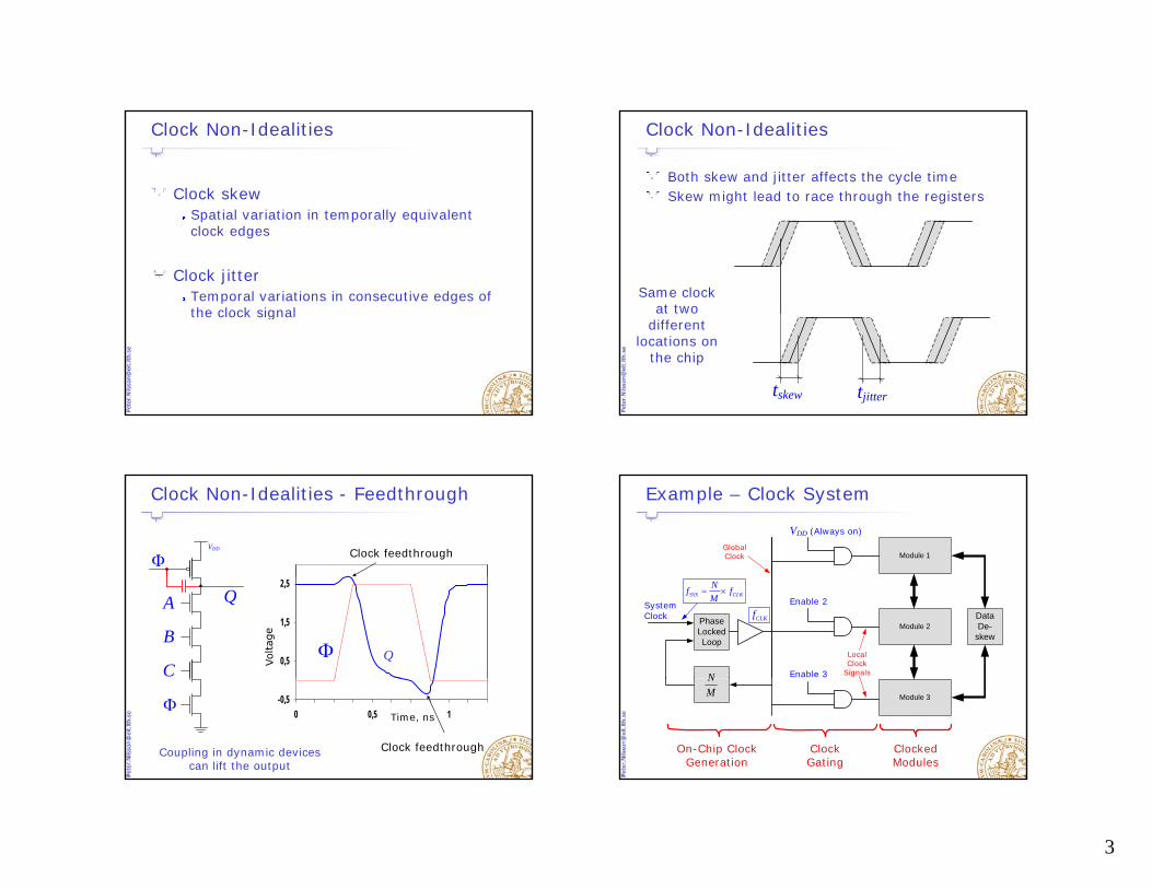
Clock Non-Idealities
Clock skewSpatial a iation in tempo all eq i alent Spatial variation in temporally equivalent clock edges
Clock jitterTemporal variations in consecutive edges of the clock signalthe clock signal
Clock Non-Idealities
Both skew and jitter affects the cycle timeSkew might lead to race through the registers
Same clock at two
tskew tjitter
different locations on
the chip
Clock Non-Idealities - Feedthrough
Clock feedthroughVDD
Φ
0,5
1,5
2,5
Q
A
C
B
Q
Φ
-0,50 0,5 1Time, ns
Clock feedthrough
Φ
Coupling in dynamic devicescan lift the output
Example – Clock System
VDD (Always on)
Module 1Global Clock
Module 2Data De-
skew
Enable 2
Enable 3
Phase Locked Loop
N
System Clock CLKf
SYS CLKNf fM
= ×
Local Clock
Signals
Module 3
NM
On-Chip Clock Generation
ClockGating
ClockedModules
4
Synchronous Pipelined Datapath
In
tpd,reg tpd1
DR1
Q
CLK
LogicBlock #1
tpd2
DR2
QLogic
Block #2
tpd3
DR3
Q DR4
QLogic
Block #3
Delay DelayDelay
The delay give clock skew
Clock Skew
10x10 mm Chip
Absolute SkewRelative Skew
Example: 15 mm wire
C = 300 fFR = 4 kΩ
tpHL = 0.69RC = 0.8 ns
Δ L = 15mm
CLK“Max frequency”
1 1 600 MHz2 2 0.8 nspHLt
= =×
Clock Skew
Negative Skew
OutREG Abs
REG Lo
g
REG
REG
In
Clock and data routing
R
Positive SkewCLK
Setup- and Hold-times
Data bus
tji tter tho ld
Clock line
tji tter tsetup ji tter ho ldji tter setup
5
Clock Skew
Ext.CLK
φ1CLK
φ2
φ1
Large skew require large non-overlap
φ1
φ2
General Clock Distribution Tree
R t
Branches
Leaves
Clock Source
Root Trunk
Have a large relative skew
Balanced Clock Net
Distributed Buffers
All wires and buffers are
carefully balanced
Clock
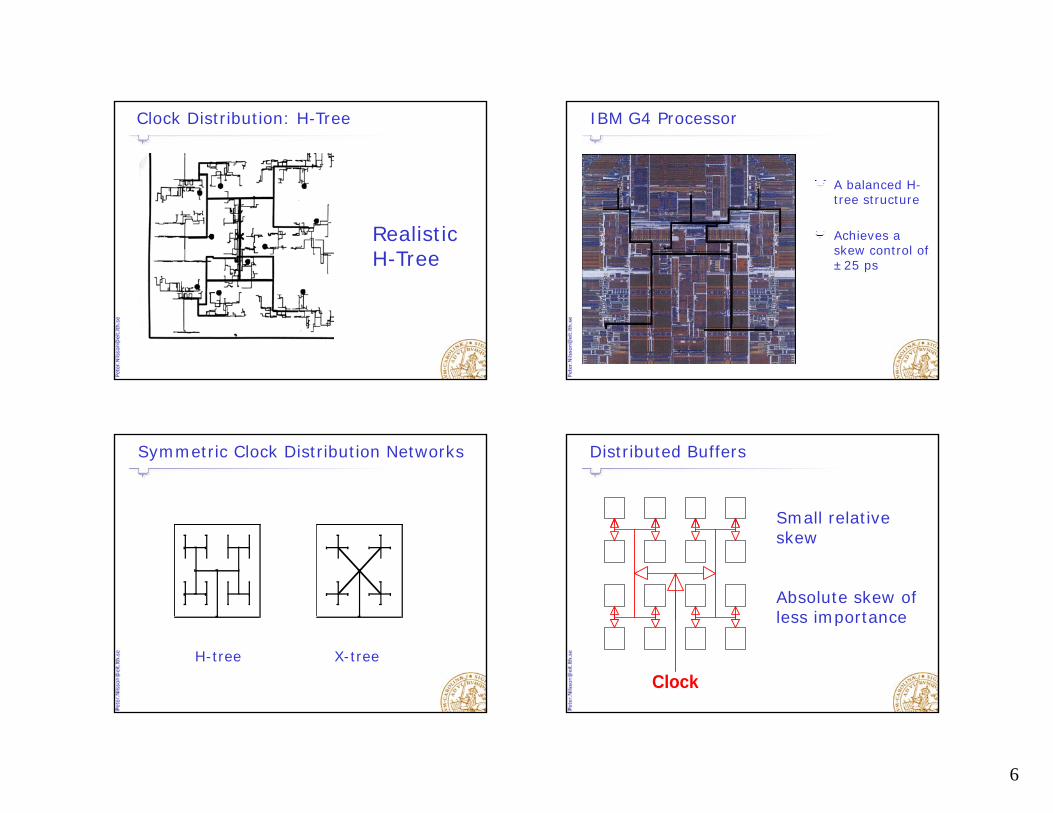
Clock Distribution: H-Tree
Small relative skew
Absolute skew of less importanceless importance
Clock
6
Clock Distribution: H-Tree
Realistic H-Tree
IBM G4 Processor
A balanced H-tree structure
Achieves a skew control of ±25 ps
Symmetric Clock Distribution Networks
H-tree X-tree
Distributed Buffers
Small relative skew
Absolute skew of less importanceless importance
Clock
7
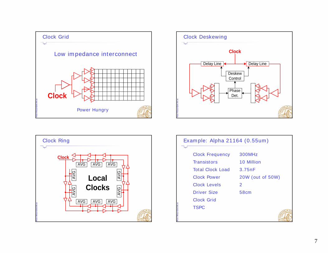
Clock Grid
Low impedance interconnect
ClockPower Hungry
Clock Deskewing
Clock
Ph
DeskewControl
Delay LineDelay Line
PhaseDet.
Clock Ring
ClockAVG AVGAVGAVG AVGAVG
AV
GA
VG
AV
GA
VG
LocalClocks
A A
AVGAVG AVG
Example: Alpha 21164 (0.55um)
Clock Frequency 300MHz
Transistors 10 Million
Total Clock Load 3.75nF
Clock Power 20W (out of 50W)
Clock Levels 2
Driver Size 58cmDriver Size 58cm
Clock Grid
TSPC
8
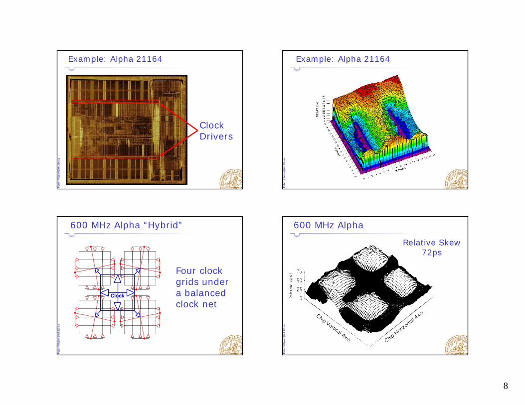
Example: Alpha 21164
ClockDrivers
Example: Alpha 21164
600 MHz Alpha “Hybrid”
Four clock grids under a balanced clock net
Clock
Relative Skew 72ps
600 MHz Alpha
9
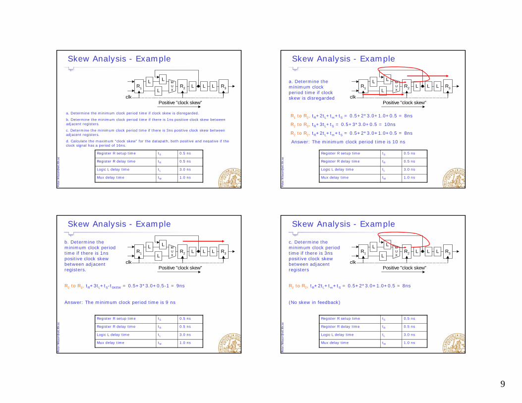
Skew Analysis - Example
R1
MUX
L L LR2 R3
L L
Llk
a. Determine the minimum clock period time if clock skew is disregarded.
b. Determine the minimum clock period time if there is 1ns positive clock skew between adjacent registers.
c. Determine the minimum clock period time if there is 3ns positive clock skew between adjacent registers.
d. Calculate the maximum “clock skew” for the datapath, both positive and negative if the
clkPositive "clock skew"
d. Calculate the maximum clock skew for the datapath, both positive and negative if the clock signal has a period of 16ns.
Register R setup time tS 0.5 ns
Register R delay time tR 0.5 ns
Logic L delay time tL 3.0 ns
Mux delay time tM 1.0 ns
R1
MUX
L L LR2 R3
L L
Llk
a. Determine the minimum clock period time if clock
Skew Analysis - Example
Answer: The minimum clock period time is 10 ns
clkPositive "clock skew"
skew is disregarded
R2 to R3, tR+3tL+tS = 0.5+3*3.0+0.5 = 10ns
R2 to R2, tR+2tL+tm+tS = 0.5+2*3.0+1.0+0.5 = 8ns
R1 to R2, tR+2tL+tm+tS = 0.5+2*3.0+1.0+0.5 = 8ns
Answer: The minimum clock period time is 10 ns
Register R setup time tS 0.5 ns
Register R delay time tR 0.5 ns
Logic L delay time tL 3.0 ns
Mux delay time tM 1.0 ns
R1
MUX
L L LR2 R3
L L
Llk
b. Determine the minimum clock period time if there is 1ns positive clock skew
Skew Analysis - Example
R2 to R3, tR+3tL+tS-tSKEW = 0.5+3*3.0+0.5-1 = 9ns
Answer: The minimum clock period time is 9 ns
clkPositive "clock skew"
between adjacent registers.
Register R setup time tS 0.5 ns
Register R delay time tR 0.5 ns
Logic L delay time tL 3.0 ns
Mux delay time tM 1.0 ns
R1
MUX
L L LR2 R3
L L
Llk
c. Determine the minimum clock period time if there is 3ns positive clock skew
Skew Analysis - Example
R2 to R2, tR+2tL+tm+tS = 0.5+2*3.0+1.0+0.5 = 8ns
(No skew in feedback)
clkPositive "clock skew"
between adjacent registers
Register R setup time tS 0.5 ns
Register R delay time tR 0.5 ns
Logic L delay time tL 3.0 ns
Mux delay time tM 1.0 ns
10
R1
MUX
L L LR2 R3
L L
Llk
d. Calculate the maximum “clock skew” for the datapath, both positive and negative if
From asynchronous domains or From synchronous domains with different clock
Synchronizing Signals (Metastability)
AsynchronousAsynchronoussystemsystem
synchronoussynchronoustt
periods
systemsystem systemsystem
synchronizationsynchronization
Metastable state: possible output from a flip-flop
Synchronizing Signals (Metastability)
Aperture window
tres is important
tres
Many designers are not aware ofmetastability
important for MTBF
Can occur if the setup tSU, hold time tH, or clock pulse width tPW of a flip-flop is not met
Synchronizing Signals (Metastability)
D QDATA IN
CLK
Q1
DATA IN
tW
tSU
trestCO
CLK
Q1
“1”
“0”
tW = Time window where input transition may cause a metastable conditiontSU = Actual clock setup time for flip-floptCO = Actual flip-flop propagation delaytres = Metastability resolution time
11
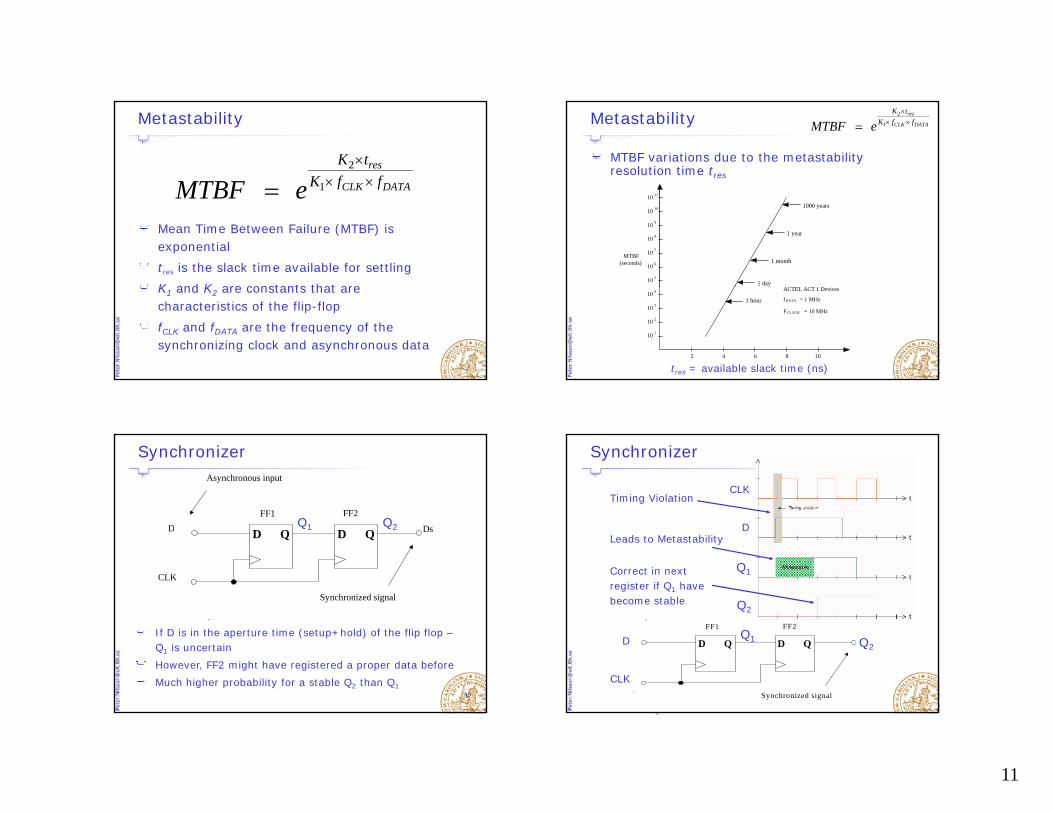
Metastability
2
1 res
CLK DATA
K tK f fMTBF e
×× ×=
Mean Time Between Failure (MTBF) is exponential
tres is the slack time available for settling
K and K are constants that are
MTBF e=
K1 and K2 are constants that are characteristics of the flip-flop
fCLK and fDATA are the frequency of the synchronizing clock and asynchronous data
MTBF variations due to the metastabilityresolution time tres
11
Metastability 2
1 res
CLK DATA
K tK f fMTBF e
×× ×=
10 5
10 6
10 7
10 8
10 9
10 10
10 11
MTBF(seconds)
1000 years
1 year
1 month
1 dayi
tres (ns)
10 1
10 2
10 3
10 4
2 4 6 8 10
1 hour fDATA = 1 MHz
FCLOCK = 10 MHz
ACTEL ACT 1 Devices
tres = available slack time (ns)
D D
FF1 FF2
Asynchronous input
Synchronizer
Q1 Q2D QD Q
CLK
Da Ds
Synchronized signal
Q1 Q2
A5
Global low-skew clockIf D is in the aperture time (setup+hold) of the flip flop –Q1 is uncertain
However, FF2 might have registered a proper data before
Much higher probability for a stable Q2 than Q1
Synchronizer
CLK
D
Timing Violation
Q1
Asynchronous input
D
Q2
Leads to Metastability
Correct in next register if Q1 have become stable
D QD Q
CLK
Da Ds
FF1 FF2
Synchronized signal
Q1 Q2D
CLK
12
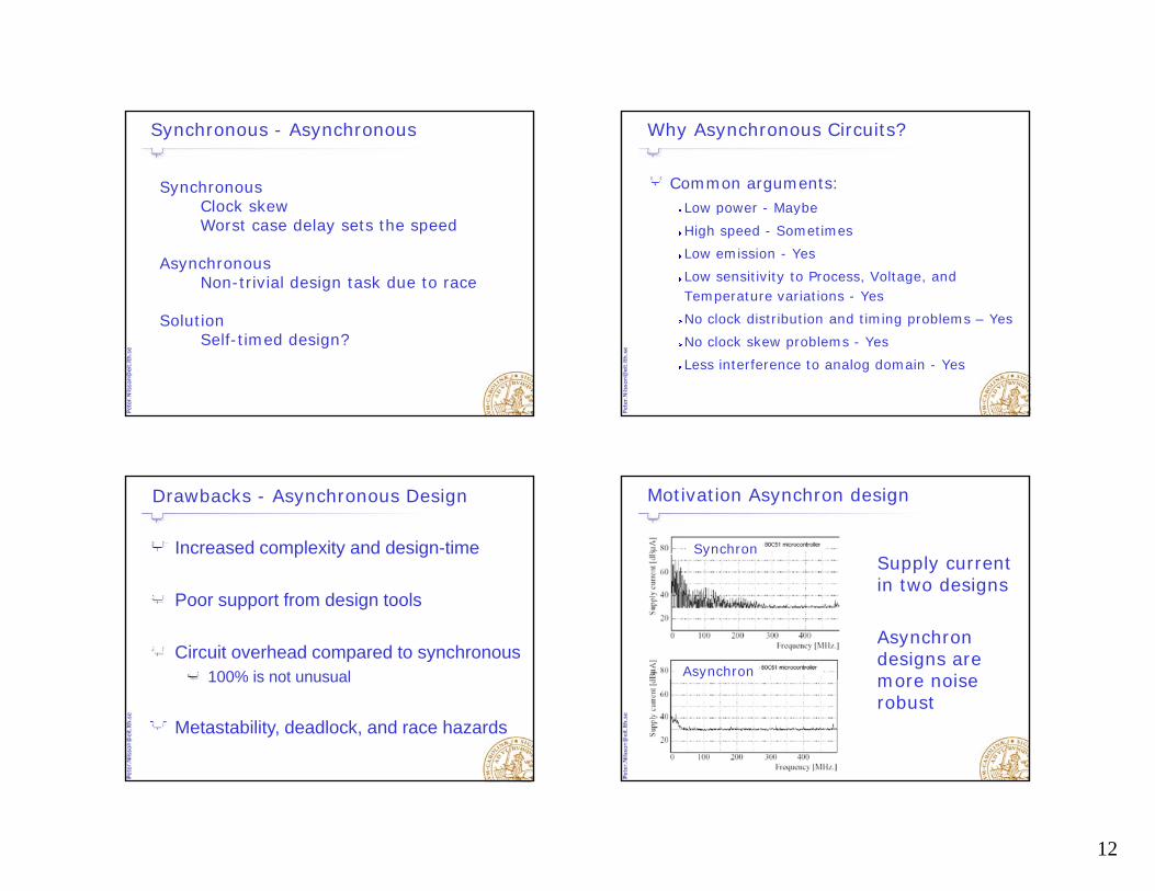
Synchronous - Asynchronous
SynchronousClock skewWorst case delay sets the speed
AsynchronousNon-trivial design task due to race
S l iSolutionSelf-timed design?
Why Asynchronous Circuits?
Common arguments:Low power - MaybeLow power Maybe
High speed - Sometimes
Low emission - Yes
Low sensitivity to Process, Voltage, and Temperature variations - Yes
N l k di t ib ti d ti i bl YNo clock distribution and timing problems – Yes
No clock skew problems - Yes
Less interference to analog domain - Yes
Drawbacks - Asynchronous Design
Increased complexity and design-time
Poor support from design tools
Circuit overhead compared to synchronous100% is not unusual100% is not unusual
Metastability, deadlock, and race hazards
Motivation Asynchron design
Supply current d
Synchron
in two designs
Asynchron designs are more noise
Asynchronmore noise robust
13
Noise in Supply Plane
Synchron DSP Asynchron DSP
Source: James Awad, Octasic Semiconductor
Asynchronous Modules
logic logic
handshake handshake
go done go donereq req req
data data data
ack ack ack
The most Basic Protocol
1.The sender issues a request 2.The receiver replies by an acknowledge 3.Then the sender sends the data
Module 1
Module 2
1. Req
2. Ack
3. Data
If the sender initiates the data transferThe transfer channel is a push-channel
If the receiver initiates the transfer The channel is a pull-channel
n
The Two-Phase Protocol
1. The sender establish stable dataOn both raising
and falling edges
(No return-to-zero 2. The sender produces a request
(No return-to-zero transitions)3. The receiver absorbs data and
produces an acknowledge
1Data
2
3Req
Ack
Cycle 1 Cycle 2
14
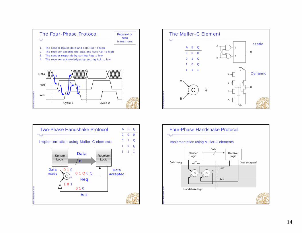
The Four-Phase Protocol
1. The sender issues data and sets Req to high2. The receiver absorbs the data and sets Ack to high3 The sender responds by setting Req to low
Return-to-zero
transitions
3. The sender responds by setting Req to low4. The receiver acknowledges by setting Ack to low
1Data
3
2
Req
Ack
Cycle 1 Cycle 2
34
The Muller-C Element
A B Q
0 0 0 Q
A
R
SStatic
0 1 Q
1 0 Q
1 1 1
A
BR
A
VDD
B
Dynamic
Q
B
CQ
B
B
A
Two-Phase Handshake Protocol
Implementation using Muller-C elements
A B Q
0 0 0
0 1 Q
1 0 Q
1 1 1
Data ready
C
Sender Logic
R
Receiver Logic
Data accepted
Data
n
00 1
1 Q0
0 QQ
1 1 1
Req
Ack
01
10 1
0
Q
Four-Phase Handshake Protocol
Implementation using Muller-C elements
Data
Data ready Data accepted
ReqS
C C
Senderlogic
Receiverlogic
Handshake logic
Ack
15
Clocking & Timing
Advanced Digital IC-Design
Clocking & Timing
ContCont.
Student Lectures
Send your slides to me, latest the night before your presentation
Preferred format - .ppt
You will be evaluated by your fiends
Please look at the template:Please look at the template:
http://www.eit.lth.se/course/eti135 -> Home Exercises
Deadline: March 8
Invited Lecture
Advanced Digital IC Design
Static timing analysis 11/02, 15.15-17.00
Design for test is canceledes g o test s ca ce ed
16
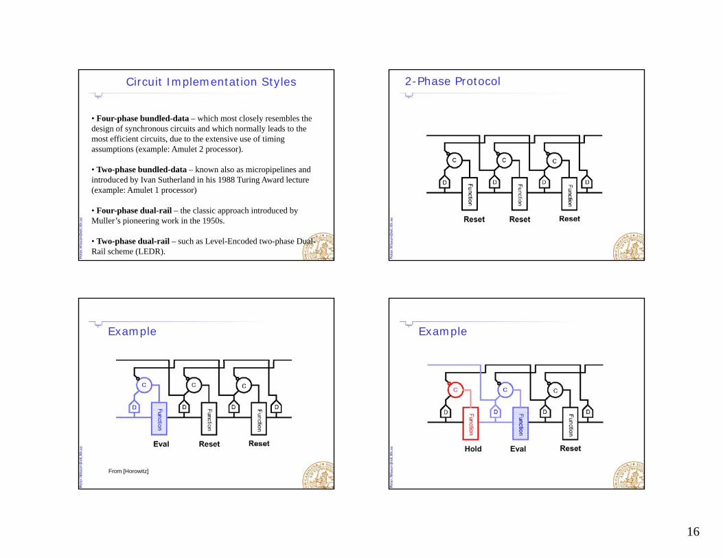
Circuit Implementation Styles
• Four-phase bundled-data – which most closely resembles the design of synchronous circuits and which normally leads to the g y ymost efficient circuits, due to the extensive use of timing assumptions (example: Amulet 2 processor).
• Two-phase bundled-data – known also as micropipelines and introduced by Ivan Sutherland in his 1988 Turing Award lecture (example: Amulet 1 processor)
• Four-phase dual-rail – the classic approach introduced by Muller’s pioneering work in the 1950s.
• Two-phase dual-rail – such as Level-Encoded two-phase Dual-Rail scheme (LEDR).
2-Phase Protocol
Example
From [Horowitz]
Example
17
Example Example
Completion Signal Generation
B0
Start
PDN PDNDual
A&AB&B
Start
B1
B
Dual Rail
Used in Phase B0 B1 B CommentPrecharge 0 0 0 Not DoneEvaluation 0 1 1 DoneEvaluation 1 0 1 DoneIllegal 1 1 - Illegal
Used in self-timed modules
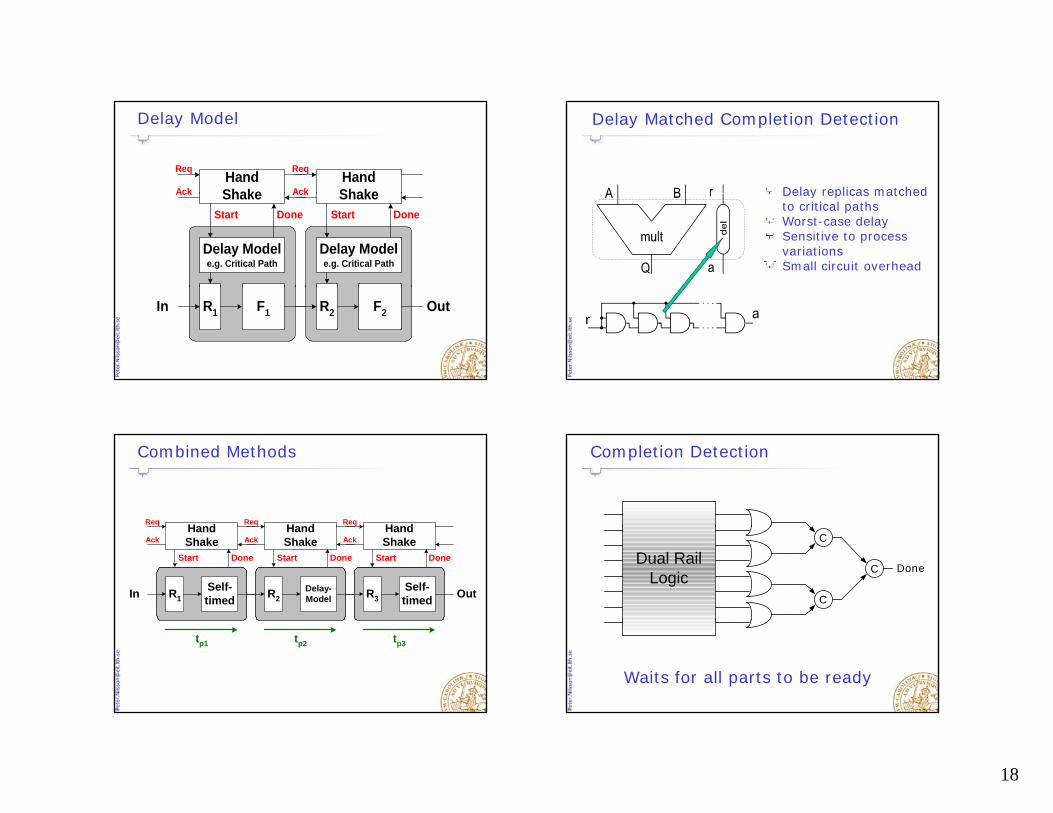
Self-Timed Pipelining
In R1 F1
HandShake
Start Done
Ack
Req
R2 F2
HandShake
Start Done
Ack
Req
R3 F3
HandShake
Start Done
Ack
Req
Out
tp1 tp3tp2
18
Delay Model
HandShakeAck
Req HandShakeAck
Req
ShakeStart Done
Ack ShakeStart Done
Ack
Delay Modele.g. Critical Path
Delay Modele.g. Critical Path
In R1 F1 R2 F2 Out
Delay Matched Completion Detection
Delay replicas matched Delay replicas matched to critical pathsWorst-case delaySensitive to process variationsSmall circuit overhead
Combined Methods
HandReq HandReq HandReq
In R1Self-timed
HandShake
Start Done
Ack
R2Delay-Model
HandShake
Start Done
Ack
R3Self-timed
HandShake
Start Done
Ack
Out
tp1 tp3tp2
Completion Detection
Done
C
C
CDual Rail
Logic
Waits for all parts to be ready
19
Other Asynchron Modules
Linear Pipelines (only one input and output)
F
F
Non-Linear Pipelines
F
F
ForkJoin
Conditional Split
Conditional Join
FF
Synchronous – Asynchronous
Global
Synchronous Asynchronous
ract
icedGALSTr
aditi
onal
Globally AsynchronousLocally Synchronous
Local
Pr
Divide into smaller synchronous blocks
Clocking becomes less troublesome for small clock domains
Globally Asynchronous Locally Synchronous to Avoid Skew