www.ti.com SLUS953A –AUGUST 2009–REVISED APRIL 2012
SYNCHRONOUS SWITCHMODE, LI-ION AND LI-POLYMER CHARGE-MANAGEMENTIC WITH INTEGRATED POWER FETs ( bqSWITCHER™)
Check for Samples: bq24105-Q1
1FEATURES DESCRIPTIONThe bqSWITCHER™ series are highly integrated Li-
23• Qualified for Automotive Applicationsion and Li-polymer switch-mode charge management
• Ideal For Highly Efficient Charger Designs For devices targeted at a wide range of portableSingle-, Two-, or Three-Cell Li-Ion and Li- applications. The bqSWITCHER™ series offersPolymer Battery Packs integrated synchronous PWM controller and power
FETs, high-accuracy current and voltage regulation,• Also for LiFePO4 Battery (see Using bq24105charge preconditioning, charge status, and chargeto Charge LiFePO4 Battery)termination, in a small, thermally enhanced QFN• Integrated Synchronous Fixed-Frequencypackage.
PWM Controller Operating at 1.1 MHzThe bqSWITCHER charges the battery in threeWith 0% to 100% Duty Cyclephases: conditioning, constant current, and constant• Integrated Power FETs For Up To 2-A Chargevoltage. Charge is terminated based on user-Rate selectable minimum current level. A programmable
• High-Accuracy Voltage and Current Regulation charge timer provides a safety backup for chargetermination. The bqSWITCHER automatically restarts• Stand-Alone (Built-In Charge Management andthe charge cycle if the battery voltage falls below anControl) Versioninternal threshold. The bqSWITCHER automatically• Status Outputs For LED or Host Processor enters sleep mode when VCC supply is removed.
Interface Indicates Charge-In-Progress, ChargeCompletion, Fault, and AC-Adapter Present
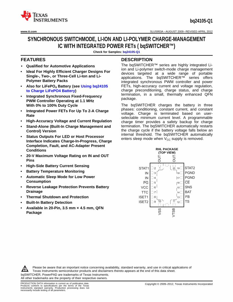
RHL PACKAGEConditions(TOP VIEW)
• 20-V Maximum Voltage Rating on IN and OUTPins
• High-Side Battery Current Sensing• Battery Temperature Monitoring• Automatic Sleep Mode for Low Power
Drainage• Thermal Shutdown and Protection• Built-In Battery Detection• Available in 20-Pin, 3.5 mm × 4.5 mm, QFN
Package
1
Please be aware that an important notice concerning availability, standard warranty, and use in critical applications ofTexas Instruments semiconductor products and disclaimers thereto appears at the end of this data sheet.
2bqSWITCHER, PowerPAD are trademarks of Texas Instruments.3All other trademarks are the property of their respective owners.
SLUS953A –AUGUST 2009–REVISED APRIL 2012 www.ti.com
This integrated circuit can be damaged by ESD. Texas Instruments recommends that all integrated circuits be handled withappropriate precautions. Failure to observe proper handling and installation procedures can cause damage.
ESD damage can range from subtle performance degradation to complete device failure. Precision integrated circuits may be moresusceptible to damage because very small parametric changes could cause the device not to meet its published specifications.
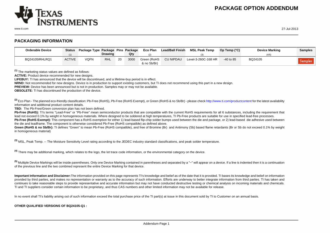
ORDERING INFORMATION (1)
TA PACKAGE (2) ORDERABLE PART NUMBER TOP-SIDE MARKING
–40°C to 85°C QFN – RHL Reel of 3000 BQ24105IRHLRQ1 BQ24105
(1) For the most current package and ordering information, see the Package Option Addendum at the end of this document, or see the TIweb site at www.ti.com.
(2) Package drawings, thermal data, and symbolization are available at www.ti.com/packaging.
ABSOLUTE MAXIMUM RATINGS (1)
over operating free-air temperature range (unless otherwise noted)
Supply voltage range (with respect to VSS) IN, VCC 20 V
STAT1, STAT2, PG, CE, SNS, BAT –0.3 V to 20 V
OUT –0.7 V to 20 V
Input voltage range (with respect to VSS and PGND) TS, TTC 7 V
VTSB 3.6 V
ISET1, ISET2 3.3 V
Voltage difference between SNS and BAT inputs (VSNS – VBAT) ±1 V
Output sink STAT1, STAT2, PG 10 mA
Output current (average) OUT 2.2 A
TA Operating free-air temperature range –40°C to 85°C
TJ Junction temperature range –40°C to 125°C
Tstg Storage temperature –65°C to 150°C
Lead temperature 1,6 mm (1/16 inch) from case for 10 seconds 300°C
(1) Stresses beyond those listed under absolute maximum ratings may cause permanent damage to the device. These are stress ratingsonly, and functional operation of the device at these or any other conditions beyond those indicated under recommended operatingconditions is not implied. Exposure to absolute-maximum-rated conditions for extended periods may affect device reliability.
PACKAGE DISSIPATION RATINGSTA < 40°C DERATING FACTORPACKAGE θJA θJC POWER RATING ABOVE TA = 40°C
RHL (1) 46.87°C/W 2.5°C/W 1.81 W 0.021 W/°C
(1) This data is based on using the JEDEC High-K board, and the exposed die pad is connected to a copper pad on the board. This isconnected to the ground plane by a 2x3 via matrix.
RECOMMENDED OPERATING CONDITIONSMIN MAX UNIT
Supply voltage, VCC and IN (Tie together) 4.35 (1) 16 (2) V
Operating junction temperature range, TJ –40 125 °C
(1) The IC continues to operate below Vmin, to 3.5 V, but the specifications are not tested and not specified.(2) The inherent switching noise voltage spikes should not exceed the absolute maximum rating on either the IN or OUT pins. A tight layout
minimizes switching noise.
ELECTRICAL CHARACTERISTICSTJ = 0°C to 125°C and recommended supply voltage range (unless otherwise stated)
tdg-SLP Deglitch time for sleep modeVCC decreasing below threshold,tFALL = 100 ns, 10-mV overdrive, 20 30 40 msSTATx pins turn off
UVLO
VUVLO-ON IC active threshold voltage VCC rising 3.15 3.30 3.50 V
IC active hysteresis VCC falling 120 150 mV
PWM
7 V ≤ VCC ≤ VCC(max) 400Internal P-channel MOSFET on-resistance
4.5 V ≤ VCC ≤ 7 V 500mΩ
7 V ≤ VCC ≤ VCC(max) 130Internal N-channel MOSFET on-resistance
4.5 V ≤ VCC ≤ 7 V 150
fOSC Oscillator frequency 1.1 MHz
Frequency accuracy –9% 9%
DMAX Maximum duty cycle 100%
DMIN Minimum duty cycle 0%
tTOD Switching delay time (turn on) 20 ns
tsyncmin Minimum synchronous FET on time 60 ns
Synchronous FET minimum current-off 50 400 mAthreshold (2)
Battery Detection
Battery detection current during time-outIDETECT VI(BAT) < VOREG – VRCH 2 mAfault
IDISCHRG1 Discharge current VSHORT < VI(BAT) < VOREG – VRCH 400 μA
tDISCHRG1 Discharge time VSHORT < VI(BAT) < VOREG – VRCH 1 s
IWAKE Wake current VSHORT < VI(BAT) < VOREG – VRCH 2 mA
tWAKE Wake time VSHORT < VI(BAT) < VOREG – VRCH 0.5 s
Begins after termination detected,IDISCHRG2 Termination discharge current 400 μAVI(BAT) ≤ VOREG
tDISCHRG2 Termination time 262 ms
Output Capacitor
Required output ceramic capacitor rangeCOUT from SNS to PGND, between inductor and 4.7 10 47 μF
RSNS
Required SNS capacitor (ceramic) at SNSCSNS 0.1 μFpin
Protection
Threshold over VOREG to turn off P-channelVOVP OVP threshold voltage MOSFET, STAT1, and STAT2 during charge 110 117 121 %VO(REG)
or termination states
ILIMIT Cycle-by-cycle current limit 2.6 3.6 4.5 A
VSHORT Short-circuit voltage threshold, BAT VI(BAT) falling 1.95 2 2.05 V/cell
ISHORT Short-circuit current VI(BAT) ≤ VSHORT 35 65 mA
TSHTDWN Thermal trip 165 °C
Thermal hysteresis 10 °C
(1) For bq24105 and bq24115 only. RIN is connected between IN and PGND pins and needed to ensure sleep entry.(2) N-channel always turns on for ~60 ns and then turns off if current is too low.
SLUS953A –AUGUST 2009–REVISED APRIL 2012 www.ti.com
TERMINAL FUNCTIONSTERMINAL
I/O DESCRIPTIONNAME NO.
Battery voltage sense input. Bypass it with a 0.1 μF capacitor to PGND if there are long inductive leadsBAT 14 I to battery.
Charger enable input. This active low input, if set high, suspends charge and places the device in theCE 16 I low-power sleep mode. Do not pull up this input to VTSB.
Output voltage analog feedback adjustment. Connect the output of a resistive voltage divider poweredFB 13 I from the battery terminals to this node to adjust the output battery voltage regulation.
IN 3, 4 I Charger input voltage.
ISET1 8 I/O Charger current set point 1 (fast charge). Use a resistor to ground to set this value.
ISET2 9 I/O Charge current set point 2 (precharge and termination), set by a resistor connected to ground.
Charge current output inductor connection. Connect a zener TVS diode between OUT pin and PGNDOUT 1, 20 O pin to clamp the voltage spike to protect the power MOSFETs during abnormal conditions.
Power-good status output (open drain). The transistor turns on when a valid VCC is detected. It is turnedPG 5 O off in the sleep mode. PG can be used to drive a LED or communicate with a host processor.
PGND 17,18 Power ground input
Charge current-sense input. Battery current is sensed via the voltage drop developed on this pin by anSNS 15 I external sense resistor in series with the battery pack. A 0.1-μF capacitor to PGND is required.
Charge status 1 (open-drain output). When the transistor turns on indicates charge in process. When itSTAT1 2 O is off and with the condition of STAT2 indicates various charger conditions (see Table 1).
Charge status 2 (open-drain output). When the transistor turns on indicates charge is done. When it isSTAT2 19 O off and with the condition of STAT1 indicates various charger conditions (see Table 1).
Temperature sense input. This input monitors its voltage against an internal threshold to determine ifTS 12 I charging is allowed. Use an NTC thermistor and a voltage divider powered from VTSB to develop this
voltage (see Figure 6).
Timer and termination control. Connect a capacitor from this node to GND to set the bqSWITCHERTTC 7 I timer. When this input is low, the timer and termination detection are disabled.
VCC 6 I Analog device input. A 0.1-μF capacitor to VSS is required.
VSS 10 Analog ground input
TS internal bias regulator voltage. Connect capacitor (with a value between a 0.1-μF and 1-μF) betweenVTSB 11 O this output and VSS.
There is an internal electrical connection between the exposed thermal pad and VSS. The exposedExposed thermal pad must be connected to the same potential as the VSS pin on the printed circuit board. ThePadThermal Pad power pad can be used as a star ground connection between VSS and PGND. A common ground plane
may be used. VSS pin must be connected to ground at all times.
*NOTE: If the TTC pin ispulled low, the safety timerand termination aredisabled; the chargercontinues to regulate, andthe STAT pins indicatecharge in progress.
If the TTC pin is pulled high(VTSB), only the safetytimer is disabled(termination is normal).
bq24105-Q1
SLUS953A –AUGUST 2009–REVISED APRIL 2012 www.ti.com
OPERATIONAL FLOW CHART
Figure 4. Stand-Alone Version Operational Flow Chart
www.ti.com SLUS953A –AUGUST 2009–REVISED APRIL 2012
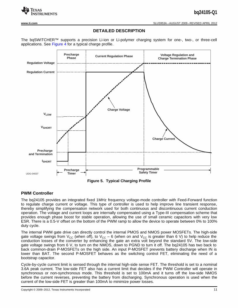
DETAILED DESCRIPTION
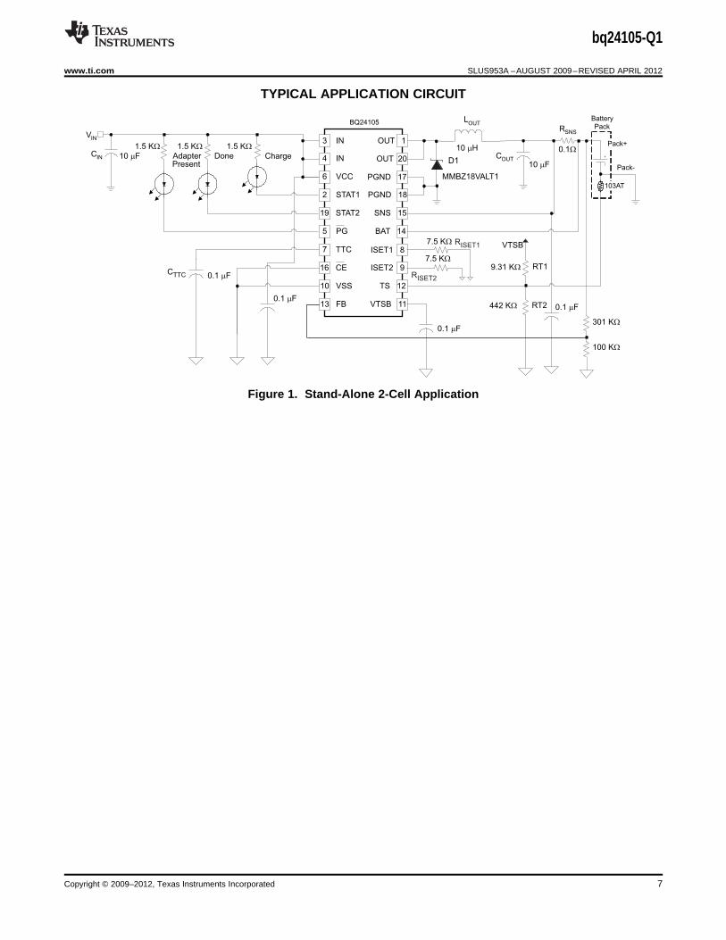
The bqSWITCHER™ supports a precision Li-ion or Li-polymer charging system for one-, two-, or three-cellapplications. See Figure 4 for a typical charge profile.
Figure 5. Typical Charging Profile
PWM Controller
The bq24105 provides an integrated fixed 1MHz frequency voltage-mode controller with Feed-Forward functionto regulate charge current or voltage. This type of controller is used to help improve line transient response,thereby simplifying the compensation network used for both continuous and discontinuous current conductionoperation. The voltage and current loops are internally compensated using a Type-III compensation scheme thatprovides enough phase boost for stable operation, allowing the use of small ceramic capacitors with very lowESR. There is a 0.5-V offset on the bottom of the PWM ramp to allow the device to operate between 0% to 100%duty cycle.
The internal PWM gate drive can directly control the internal PMOS and NMOS power MOSFETs. The high-sidegate voltage swings from VCC (when off), to VCC – 6 (when on and VCC is greater than 6 V) to help reduce theconduction losses of the converter by enhancing the gate an extra volt beyond the standard 5V. The low-sidegate voltage swings from 6 V, to turn on the NMOS, down to PGND to turn it off. The bq24105 has two back toback common-drain P-MOSFETs on the high side. An input P-MOSFET prevents battery discharge when IN islower than BAT. The second P-MOSFET behaves as the switching control FET, eliminating the need of abootstrap capacitor.
Cycle-by-cycle current limit is sensed through the internal high-side sense FET. The threshold is set to a nominal3.6A peak current. The low-side FET also has a current limit that decides if the PWM Controller will operate insynchronous or non-synchronous mode. This threshold is set to 100mA and it turns off the low-side NMOSbefore the current reverses, preventing the battery from discharging. Synchronous operation is used when thecurrent of the low-side FET is greater than 100mA to minimize power losses.
SLUS953A –AUGUST 2009–REVISED APRIL 2012 www.ti.com
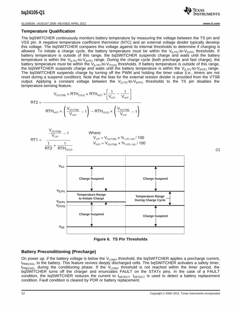
Temperature Qualification
The bqSWITCHER continuously monitors battery temperature by measuring the voltage between the TS pin andVSS pin. A negative temperature coefficient thermistor (NTC) and an external voltage divider typically developthis voltage. The bqSWITCHER compares this voltage against its internal thresholds to determine if charging isallowed. To initiate a charge cycle, the battery temperature must be within the V(LTF)-to-V(HTF) thresholds. Ifbattery temperature is outside of this range, the bqSWITCHER suspends charge and waits until the batterytemperature is within the V(LTF)-to-V(HTF) range. During the charge cycle (both precharge and fast charge), thebattery temperature must be within the V(LTF)-to-V(TCO) thresholds. If battery temperature is outside of this range,the bqSWITCHER suspends charge and waits until the battery temperature is within the V(LTF)-to-V(HTF) range.The bqSWITCHER suspends charge by turning off the PWM and holding the timer value (i.e., timers are notreset during a suspend condition). Note that the bias for the external resistor divider is provided from the VTSBoutput. Applying a constant voltage between the V(LTF)-to-V(HTF) thresholds to the TS pin disables thetemperature-sensing feature.
(1)
Figure 6. TS Pin Thresholds
Battery Preconditioning (Precharge)
On power up, if the battery voltage is below the VLOWV threshold, the bqSWITCHER applies a precharge current,IPRECHG, to the battery. This feature revives deeply discharged cells. The bqSWITCHER activates a safety timer,tPRECHG, during the conditioning phase. If the VLOWV threshold is not reached within the timer period, thebqSWITCHER turns off the charger and enunciates FAULT on the STATx pins. In the case of a FAULTcondition, the bqSWITCHER reduces the current to IDETECT. IDETECT is used to detect a battery replacementcondition. Fault condition is cleared by POR or battery replacement.
www.ti.com SLUS953A –AUGUST 2009–REVISED APRIL 2012
The magnitude of the precharge current, IO(PRECHG), is determined by the value of programming resistor, R(ISET2),connected to the ISET2 pin.
(2)
whereRSNS is the external current-sense resistorV(ISET2) is the output voltage of the ISET2 pinK(ISET2) is the V/A gain factorV(ISET2) and K(ISET2) are specified in the Electrical Characteristics table.
Battery Charge Current
The battery charge current, IO(CHARGE), is established by setting the external sense resistor, R(SNS), and theresistor, R(ISET1), connected to the ISET1 pin.
In order to set the current, first choose R(SNS) based on the regulation threshold VIREG across this resistor. Thebest accuracy is achieved when the VIREG is between 100 mV and 200 mV.
(3)
If the results is not a standard sense resistor value, choose the next larger value. Using the selected standardvalue, solve for VIREG. Once the sense resistor is selected, the ISET1 resistor can be calculated using thefollowing equation:
(4)
Battery Voltage Regulation
The voltage regulation feedback occurs through the BAT pin. This input is tied directly to the positive side of thebattery pack. The bqSWITCHER monitors the battery-pack voltage between the BAT and VSS pins.
Output regulation voltage is specified as:
(5)
where R1 and R2 are resistor divider from BAT to FB and FB to VSS, respectively.
SLUS953A –AUGUST 2009–REVISED APRIL 2012 www.ti.com
Charge Termination and Recharge
The bqSWITCHER monitors the charging current during the voltage regulation phase. Once the terminationthreshold, ITERM, is detected, the bqSWITCHER terminates charge. The termination current level is selected bythe value of programming resistor, R(ISET2), connected to the ISET2 pin.
(7)
whereR(SNS) is the external current-sense resistorVTERM is the output of the ISET2 pinK(ISET2) is the A/V gain factorVTERM and K(ISET2) are specified in the Electrical Characteristics table
As a safety backup, the bqSWITCHER also provides a programmable charge timer. The charge time isprogrammed by the value of a capacitor connected between the TTC pin and GND by the following formula:
(8)
whereC(TTC) is the capacitor connected to the TTC pinK(TTC) is the multiplier
A new charge cycle is initiated when one of the following conditions is detected:• The battery voltage falls below the VRCH threshold.• Power-on reset (POR), if battery voltage is below the VRCH threshold• CE toggle• TTC pin, described as follows.
In order to disable the charge termination and safety timer, the user can pull the TTC input below the VTTC_ENthreshold. Going above this threshold enables the termination and safety timer features and also resets the timer.Tying TTC high disables the safety timer only.
www.ti.com SLUS953A –AUGUST 2009–REVISED APRIL 2012
Sleep Mode
The bqSWITCHER enters the low-power sleep mode if the VCC pin is removed from the circuit. This featureprevents draining the battery during the absence of VCC.
Charge Status Outputs
The open-drain STAT1 and STAT2 outputs indicate various charger operations as shown in Table 1. Thesestatus pins can be used to drive LEDs or communicate to the host processor. Note that OFF indicates that theopen-drain transistor is turned off.
Table 1. Status Pins Summary
Charge State STAT1 STAT2
Charge-in-progress ON OFF
Charge complete OFF ON
Charge suspend, timer fault, overvoltage, sleep mode, battery absent OFF OFF
Table 2. Status Pins Summary
Charge State STAT1 STAT2
Battery absent OFF OFF
Charge-in-progress ON OFF
Charge complete OFF ON
Battery over discharge, VI(BAT) < V(SC) ON/OFF (0.5 Hz) OFF
Charge suspend (due to TS pin and internal thermal protection) ON/OFF (0.5 Hz) OFF
Precharge timer fault ON/OFF (0.5 Hz) OFF
Fast charge timer fault ON/OFF (0.5 Hz) OFF
Sleep mode OFF OFF
PG Output
The open-drain PG (power good) indicates when the AC-to-DC adapter (i.e., VCC) is present. The output turns onwhen sleep-mode exit threshold, VSLP-EXIT, is detected. This output is turned off in the sleep mode. The PG pincan be used to drive an LED or communicate to the host processor.
CE Input (Charge Enable)
The CE digital input is used to disable or enable the charge process. A low-level signal on this pin enables thecharge and a high-level VCC signal disables the charge. A high-to-low transition on this pin also resets all timersand fault conditions. Note that the CE pin cannot be pulled up to VTSB voltage. This may create power-upissues.
Recovery method: bqSWITCHER waits for the battery voltage to fall below the recharge threshold. This couldhappen as a result of a load on the battery, self-discharge or battery removal. Once the battery falls below therecharge threshold, the bqSWITCHER clears the fault and enters the battery absent detection routine. A POR orCE toggle also clears the fault.
Condition 2 Charge voltage below recharge threshold (VOREG – VRCH) and timeout fault occurs
Recovery method: Under this scenario, the bqSWITCHER applies the IDETECT current. This small current is usedto detect a battery removal condition and remains on as long as the battery voltage stays below the rechargethreshold. If the battery voltage goes above the recharge threshold, then the bqSWITCHER disables the IDETECTcurrent and executes the recovery method described in Condition 1. Once the battery falls below the rechargethreshold, the bqSWITCHER clears the fault and enters the battery absent detection routine. A POR or CE togglealso clears the fault.
Output Overvoltage Protection
The bqSWITCHER provides a built-in overvoltage protection to protect the device and other components againstdamages if the battery voltage gets too high, as when the battery is suddenly removed. When an overvoltagecondition is detected, this feature turns off the PWM and STATx pins. The fault is cleared once VIBAT drops to therecharge threshold (VOREG – VRCH).
Inductor, Capacitor, and Sense Resistor Selection Guidelines
The bqSWITCHER provides internal loop compensation. With this scheme, best stability occurs when LCresonant frequency, fo is approximately 16 kHz (8 kHz to 32 kHz). Equation 9 can be used to calculate the valueof the output inductor and capacitor. Table 3 provides a summary of typical component values for various chargerates.
Detection routine runs on power upand if VBAT drops below refreshthreshold due to removing batteryor discharging battery.
VI(BAT) >VO(REG)-VRCH
bq24105-Q1
www.ti.com SLUS953A –AUGUST 2009–REVISED APRIL 2012
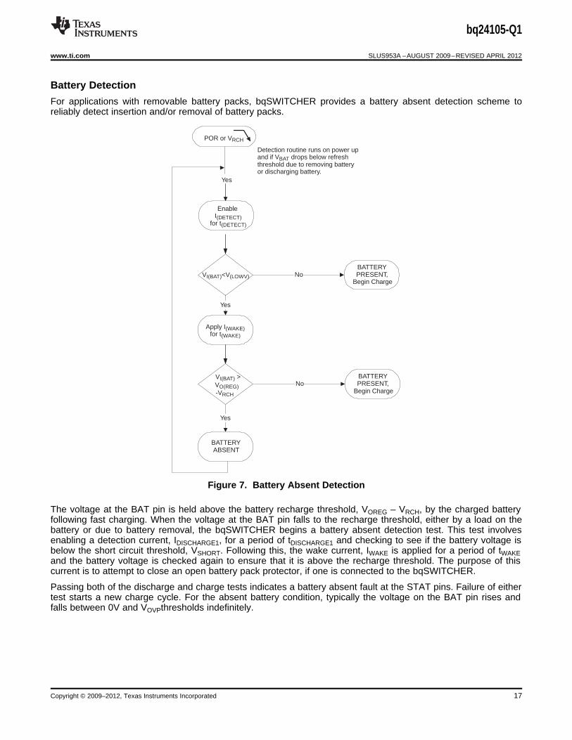
Battery Detection
For applications with removable battery packs, bqSWITCHER provides a battery absent detection scheme toreliably detect insertion and/or removal of battery packs.
Figure 7. Battery Absent Detection
The voltage at the BAT pin is held above the battery recharge threshold, VOREG – VRCH, by the charged batteryfollowing fast charging. When the voltage at the BAT pin falls to the recharge threshold, either by a load on thebattery or due to battery removal, the bqSWITCHER begins a battery absent detection test. This test involvesenabling a detection current, IDISCHARGE1, for a period of tDISCHARGE1 and checking to see if the battery voltage isbelow the short circuit threshold, VSHORT. Following this, the wake current, IWAKE is applied for a period of tWAKEand the battery voltage is checked again to ensure that it is above the recharge threshold. The purpose of thiscurrent is to attempt to close an open battery pack protector, if one is connected to the bqSWITCHER.
Passing both of the discharge and charge tests indicates a battery absent fault at the STAT pins. Failure of eithertest starts a new charge cycle. For the absent battery condition, typically the voltage on the BAT pin rises andfalls between 0V and VOVPthresholds indefinitely.
SLUS953A –AUGUST 2009–REVISED APRIL 2012 www.ti.com
Figure 8. Battery Detect Timing Diagram
Battery Detection Example
In order to detect a no battery condition during the discharge and wake tests, the maximum output capacitanceshould not exceed the following:a. Discharge (IDISCHRG1 = 400 μA, tDISCHRG1 = 1s, VSHORT = 2V)
(10)
b. Wake (IWAKE = 2 mA, tWAKE = 0.5 s, VOREG – VRCH = 4.1V)
(11)
Based on these calculations the recommended maximum output capacitance to ensure proper operation of thebattery detection scheme is 100 μF which will allow for process and temperature variations.
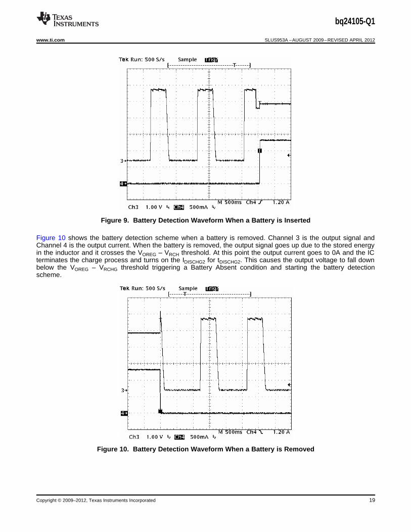
Figure 9 shows the battery detection scheme when a battery is inserted. Channel 3 is the output signal andChannel 4 is the output current. The output signal switches between VOREG and GND until a battery is inserted.Once the battery is detected, the output current increases from 0A to 1.3A, which is the programmed chargecurrent for this application.
www.ti.com SLUS953A –AUGUST 2009–REVISED APRIL 2012
Figure 9. Battery Detection Waveform When a Battery is Inserted
Figure 10 shows the battery detection scheme when a battery is removed. Channel 3 is the output signal andChannel 4 is the output current. When the battery is removed, the output signal goes up due to the stored energyin the inductor and it crosses the VOREG – VRCH threshold. At this point the output current goes to 0A and the ICterminates the charge process and turns on the IDISCHG2 for tDISCHG2. This causes the output voltage to fall downbelow the VOREG – VRCHG threshold triggering a Battery Absent condition and starting the battery detectionscheme.
Figure 10. Battery Detection Waveform When a Battery is Removed
SLUS953A –AUGUST 2009–REVISED APRIL 2012 www.ti.com
Current Sense Amplifier
A current sense amplifier feature that translates the charge current into a DC voltage is offered. Figure 11 is ablock diagram of this feature.
Figure 11. Current Sense Amplifier
The voltage on the ISET2 pin can be used to calculate the charge current. Equation 12 shows the relationshipbetween the ISET2 voltage and the charge current:
(12)
This feature can be used to monitor the charge current (Figure 12) during the current regulation phase(Fastcharge only) and the voltage regulation phase. The schematic for the application circuit for this waveform isshown in Figure 14
Figure 12. Current Sense Amplifier Charge Current Waveform
www.ti.com SLUS953A –AUGUST 2009–REVISED APRIL 2012
bqSWITCHER SYSTEM DESIGN EXAMPLE
The following section provides a detailed system design example for the bq24100.
System Design Specifications:• VIN = 16V• VBAT = 4.2V (1-Cell)• ICHARGE = 1.33 A• IPRECHARGE = ITERM = 133 mA• Safety Timer = 5 hours• Inductor Ripple Current = 30% of Fast Charge Current• Initiate Charge Temperature = 0°C to 45°C1. Determine the inductor value (LOUT) for the specified charge current ripple:
(13)
Set the output inductor to standard 10 μH. Calculate the total ripple current with using the 10 μH inductor:
(14)
Calculate the maximum output current (peak current):
(15)
Use standard 10 μH inductor with a saturation current higher than 1.471A. (i.e., Sumida CDRH74-100)
SLUS953A –AUGUST 2009–REVISED APRIL 2012 www.ti.com
2. Determine the output capacitor value (OUT) using 16 kHz as the resonant frequency:
(16)
Use standard value 10 μF, 25V, X5R, ±20% ceramic capacitor (i.e., Panasonic 1206 ECJ-3YB1E106M3. Determine the sense resistor using the following equation:
(17)
In order to get better current regulation accuracy (±10%), let VRSNS be between 100 mV and 200 mV. UseVRSNS = 100 mV and calculate the value for the sense resistor.
(18)
This value is not standard in resistors. If this happens, then choose the next larger value which in this case is0.1Ω. Using the same equation (15) the actual VRSNS will be 133mV. Calculate the power dissipation on thesense resistor:
(19)
Select standard value 100 mΩ, 0.25W 0805, 1206 or 2010 size, high precision sensing resistor. (i.e., VishayCRCW1210-0R10F)
4. Determine ISET 1 resistor using the following equation:
(20)
Select standard value 7.5 kΩ, 1/16W ±1% resistor (i.e., Vishay CRCWD0603-7501-F)5. Determine ISET 2 resistor using the following equation:
(21)
Select standard value 7.5 kΩ, 1/16W ±1% resistor (i.e., Vishay CRCWD0603-7501-F)
www.ti.com SLUS953A –AUGUST 2009–REVISED APRIL 2012
6. Determine TTC capacitor (TTC) for the 5.0 hours safety timer using the following equation:
(22)
Select standard value 100 nF, 16V, X7R, ±10% ceramic capacitor (i.e., Panasonic ECJ-1VB1C104K). Usingthis capacitor the actual safety timer will be 4.3 hours.
7. Determine TS resistor network for an operating temperature range from 0°C to 45°C.
Figure 13. TS Resistor Network
Assuming a 103AT NTC Thermistor on the battery pack, determine the values for RT1 and RT2 using thefollowing equations:
SLUS953A –AUGUST 2009–REVISED APRIL 2012 www.ti.com
APPLICATION INFORMATION
Charging Battery and Powering System Without Affecting Battery Charge and Termination
Figure 14. Application Circuit for Charging a Battery and Powering a System Without AffectingTermination
The bqSWITCHER was designed as a stand-alone battery charger but can be easily adapted to power a systemload, while considering a few minor issues.
Advantages:1. The charger controller is based only on what current goes through the current-sense resistor (so precharge,
constant current, and termination all work well), and is not affected by the system load.2. The input voltage has been converted to a usable system voltage with good efficiency from the input.3. Extra external FETs are not needed to switch power source to the battery.4. The TTC pin can be grounded to disable termination and keep the converter running and the battery fully
charged, or let the switcher terminate when the battery is full and then run off of the battery via the senseresistor.
Other Issues:1. If the system load current is large (≥ 1 A), the IR drop across the battery impedance causes the battery
voltage to drop below the refresh threshold and start a new charge. The charger would then terminate due tolow charge current. Therefore, the charger would cycle between charging and termination. If the load issmaller, the battery would have to discharge down to the refresh threshold resulting in a much slowercycling. Note that grounding the TTC pin keeps the converter on continuously.
2. If TTC is grounded, the battery is kept at 4.2 V (not much different than leaving a fully charged battery setunloaded).
3. Efficiency declines 2-3% hit when discharging through the sense resistor to the system.
www.ti.com SLUS953A –AUGUST 2009–REVISED APRIL 2012
Using bq24105 to Charge LiFePO4 Battery
The LiFePO4 battery has many unique features such as a high thermal runaway temperature, discharge currentcapability, and charge current. These special features make it attractive in many applications such as powertools. The recommended charge voltage is 3.6 V and termination current is 50 mA. Figure 15 shows anapplication circuit for charging one cell LiFePO4 using bq24105. The charge voltage is 3.6 V and rechargevoltage is 3.516 V. The fast charging current is set to 1.33 A while the termination current is 50 mA. This circuitcan be easily changed to support two or three cell applications. However, only 84 mV difference betweenregulation set point and rechargeable threshold makes it frequently enter into recharge mode when small loadcurrent is applied. This can be solved by lower down the recharge voltage threshold to 200 mV to dischargemore energy from the battery before it enters recharge mode again. See the application report, Using thebq24105/25 to Charge LiFePO4 Battery (SLUA443), for additional details. The recharge threshold should beselected according to real application conditions.
SLUS953A –AUGUST 2009–REVISED APRIL 2012 www.ti.com
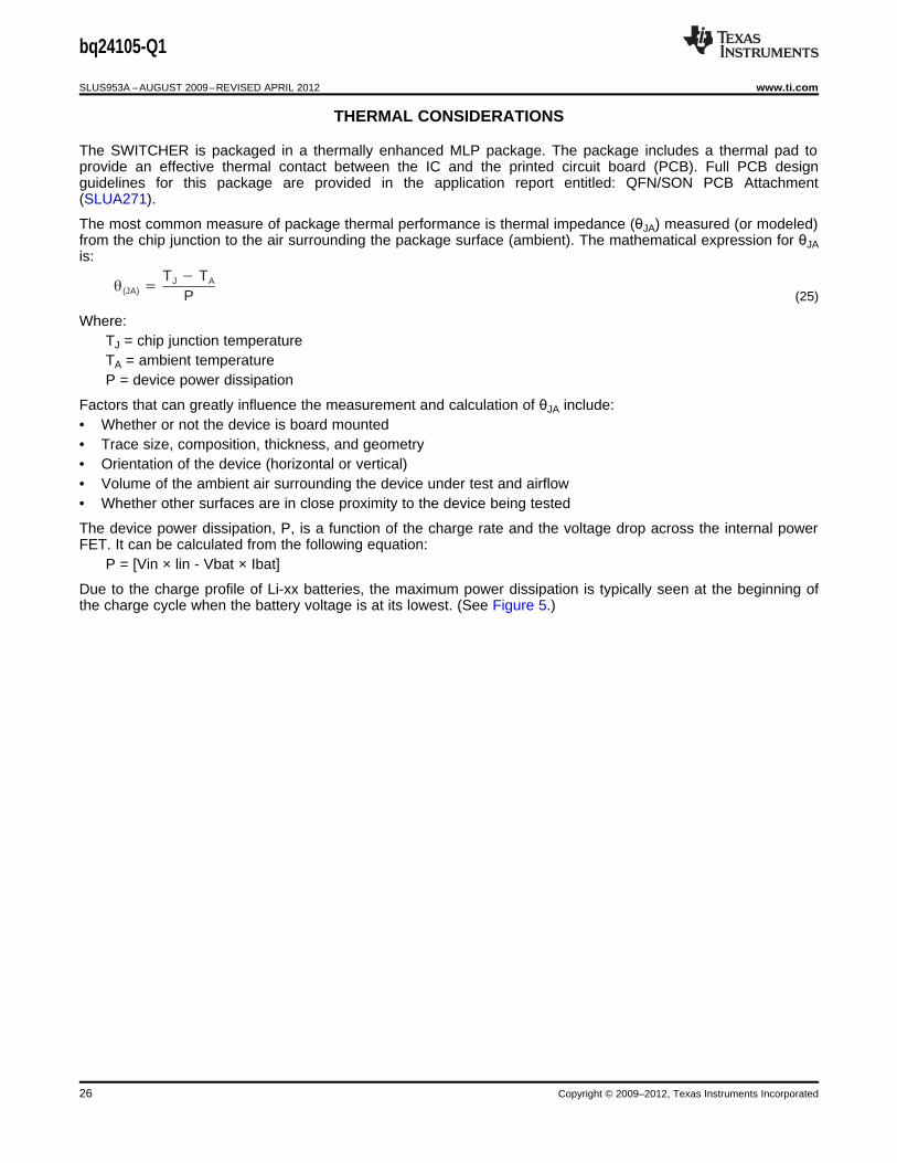
THERMAL CONSIDERATIONS
The SWITCHER is packaged in a thermally enhanced MLP package. The package includes a thermal pad toprovide an effective thermal contact between the IC and the printed circuit board (PCB). Full PCB designguidelines for this package are provided in the application report entitled: QFN/SON PCB Attachment(SLUA271).
The most common measure of package thermal performance is thermal impedance (θJA) measured (or modeled)from the chip junction to the air surrounding the package surface (ambient). The mathematical expression for θJAis:
Factors that can greatly influence the measurement and calculation of θJA include:• Whether or not the device is board mounted• Trace size, composition, thickness, and geometry• Orientation of the device (horizontal or vertical)• Volume of the ambient air surrounding the device under test and airflow• Whether other surfaces are in close proximity to the device being tested
The device power dissipation, P, is a function of the charge rate and the voltage drop across the internal powerFET. It can be calculated from the following equation:
P = [Vin × lin - Vbat × Ibat]
Due to the charge profile of Li-xx batteries, the maximum power dissipation is typically seen at the beginning ofthe charge cycle when the battery voltage is at its lowest. (See Figure 5.)
www.ti.com SLUS953A –AUGUST 2009–REVISED APRIL 2012
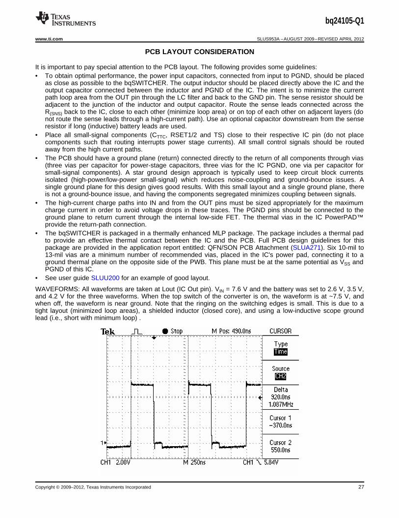
PCB LAYOUT CONSIDERATION
It is important to pay special attention to the PCB layout. The following provides some guidelines:• To obtain optimal performance, the power input capacitors, connected from input to PGND, should be placed
as close as possible to the bqSWITCHER. The output inductor should be placed directly above the IC and theoutput capacitor connected between the inductor and PGND of the IC. The intent is to minimize the currentpath loop area from the OUT pin through the LC filter and back to the GND pin. The sense resistor should beadjacent to the junction of the inductor and output capacitor. Route the sense leads connected across theR(SNS) back to the IC, close to each other (minimize loop area) or on top of each other on adjacent layers (donot route the sense leads through a high-current path). Use an optional capacitor downstream from the senseresistor if long (inductive) battery leads are used.
• Place all small-signal components (CTTC, RSET1/2 and TS) close to their respective IC pin (do not placecomponents such that routing interrupts power stage currents). All small control signals should be routedaway from the high current paths.
• The PCB should have a ground plane (return) connected directly to the return of all components through vias(three vias per capacitor for power-stage capacitors, three vias for the IC PGND, one via per capacitor forsmall-signal components). A star ground design approach is typically used to keep circuit block currentsisolated (high-power/low-power small-signal) which reduces noise-coupling and ground-bounce issues. Asingle ground plane for this design gives good results. With this small layout and a single ground plane, thereis not a ground-bounce issue, and having the components segregated minimizes coupling between signals.
• The high-current charge paths into IN and from the OUT pins must be sized appropriately for the maximumcharge current in order to avoid voltage drops in these traces. The PGND pins should be connected to theground plane to return current through the internal low-side FET. The thermal vias in the IC PowerPAD™provide the return-path connection.
• The bqSWITCHER is packaged in a thermally enhanced MLP package. The package includes a thermal padto provide an effective thermal contact between the IC and the PCB. Full PCB design guidelines for thispackage are provided in the application report entitled: QFN/SON PCB Attachment (SLUA271). Six 10-mil to13-mil vias are a minimum number of recommended vias, placed in the IC's power pad, connecting it to aground thermal plane on the opposite side of the PWB. This plane must be at the same potential as VSS andPGND of this IC.
• See user guide SLUU200 for an example of good layout.
WAVEFORMS: All waveforms are taken at Lout (IC Out pin). VIN = 7.6 V and the battery was set to 2.6 V, 3.5 V,and 4.2 V for the three waveforms. When the top switch of the converter is on, the waveform is at ~7.5 V, andwhen off, the waveform is near ground. Note that the ringing on the switching edges is small. This is due to atight layout (minimized loop areas), a shielded inductor (closed core), and using a low-inductive scope groundlead (i.e., short with minimum loop) .
SLUS953A –AUGUST 2009–REVISED APRIL 2012 www.ti.com
Precharge: The current is low in precharge; so, the bottom synchronous FET turns off after its minimum on-timewhich explains the step between ≉0 V and -0.5 V. When the bottom FET and top FET are off, the currentconducts through the body diode of the bottom FET which results in a diode drop below the ground potential.The initial negative spike is the delay turning on the bottom FET, which is to prevent shoot-through current as thetop FET is turning off.
Fast Charge: This is captured during the constant-current phase. The two negative spikes are the result of theshort delay when switching between the top and bottom FETs. The break-before-make action prevents currentshoot-through and results in a body diode drop below ground potential during the break time.
Charge during Voltage Regulation and Approaching Termination: Note that this waveform is similar to theprecharge waveform. The difference is that the battery voltage is higher so the duty cycle is slightly higher. Thebottom FET stays on longer because there is more of a current load than during precharge; it takes longer for theinductor current to ramp down to the current threshold where the synchronous FET is disabled.
BQ24105IRHLRQ1 ACTIVE VQFN RHL 20 3000 Green (RoHS& no Sb/Br)
CU NIPDAU Level-3-260C-168 HR -40 to 85 BQ24105
(1) The marketing status values are defined as follows:ACTIVE: Product device recommended for new designs.LIFEBUY: TI has announced that the device will be discontinued, and a lifetime-buy period is in effect.NRND: Not recommended for new designs. Device is in production to support existing customers, but TI does not recommend using this part in a new design.PREVIEW: Device has been announced but is not in production. Samples may or may not be available.OBSOLETE: TI has discontinued the production of the device.
(2) Eco Plan - The planned eco-friendly classification: Pb-Free (RoHS), Pb-Free (RoHS Exempt), or Green (RoHS & no Sb/Br) - please check http://www.ti.com/productcontent for the latest availabilityinformation and additional product content details.TBD: The Pb-Free/Green conversion plan has not been defined.Pb-Free (RoHS): TI's terms "Lead-Free" or "Pb-Free" mean semiconductor products that are compatible with the current RoHS requirements for all 6 substances, including the requirement thatlead not exceed 0.1% by weight in homogeneous materials. Where designed to be soldered at high temperatures, TI Pb-Free products are suitable for use in specified lead-free processes.Pb-Free (RoHS Exempt): This component has a RoHS exemption for either 1) lead-based flip-chip solder bumps used between the die and package, or 2) lead-based die adhesive used betweenthe die and leadframe. The component is otherwise considered Pb-Free (RoHS compatible) as defined above.Green (RoHS & no Sb/Br): TI defines "Green" to mean Pb-Free (RoHS compatible), and free of Bromine (Br) and Antimony (Sb) based flame retardants (Br or Sb do not exceed 0.1% by weightin homogeneous material)
(3) MSL, Peak Temp. -- The Moisture Sensitivity Level rating according to the JEDEC industry standard classifications, and peak solder temperature.
(4) There may be additional marking, which relates to the logo, the lot trace code information, or the environmental category on the device.
(5) Multiple Device Markings will be inside parentheses. Only one Device Marking contained in parentheses and separated by a "~" will appear on a device. If a line is indented then it is a continuationof the previous line and the two combined represent the entire Device Marking for that device.
Important Information and Disclaimer:The information provided on this page represents TI's knowledge and belief as of the date that it is provided. TI bases its knowledge and belief on informationprovided by third parties, and makes no representation or warranty as to the accuracy of such information. Efforts are underway to better integrate information from third parties. TI has taken andcontinues to take reasonable steps to provide representative and accurate information but may not have conducted destructive testing or chemical analysis on incoming materials and chemicals.TI and TI suppliers consider certain information to be proprietary, and thus CAS numbers and other limited information may not be available for release.
In no event shall TI's liability arising out of such information exceed the total purchase price of the TI part(s) at issue in this document sold by TI to Customer on an annual basis.
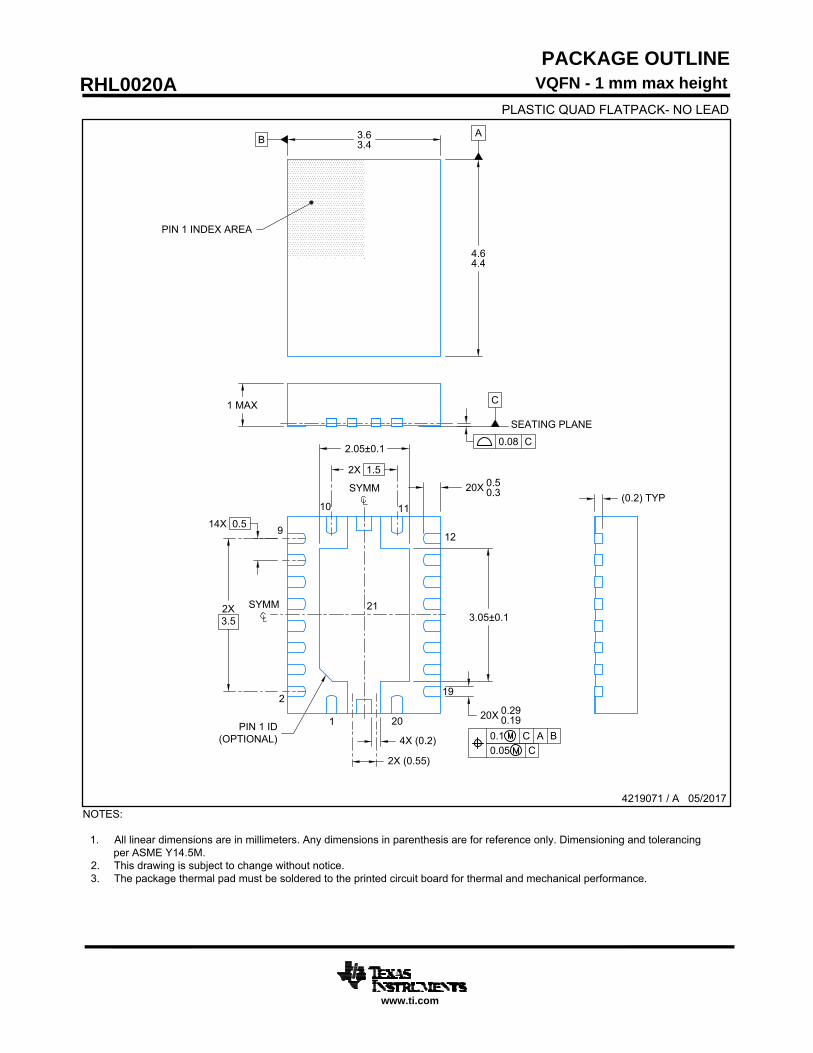
1. All linear dimensions are in millimeters. Any dimensions in parenthesis are for reference only. Dimensioning and tolerancingper ASME Y14.5M.
2. This drawing is subject to change without notice.3. The package thermal pad must be soldered to the printed circuit board for thermal and mechanical performance.
PACKAGE OUTLINE
4219071 / A 05/2017
www.ti.com
VQFN - 1 mm max height
PLASTIC QUAD FLATPACK- NO LEAD
RHL0020A
A
0.08 C
0.1 C A B0.05 C
B
SYMM
SYMM
PIN 1 INDEX AREA
SEATING PLANE
C
1PIN 1 ID(OPTIONAL)
2.05±0.1
3.05±0.1
3.63.4
4.64.4
1 MAX
(0.2) TYP
2X (0.55)
2X3.5
14X 0.5
2
9
10 11
12
19
20
2X 1.5
4X (0.2)
20X 0.290.19
20X 0.50.3
21
AutoCAD SHX Text
AutoCAD SHX Text
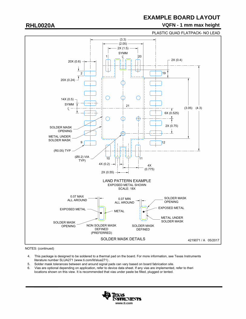
NOTES: (continued)
4. This package is designed to be soldered to a thermal pad on the board. For more information, see Texas Instrumentsliterature number SLUA271 (www.ti.com/lit/slua271) .
5. Solder mask tolerances between and around signal pads can vary based on board fabrication site.6. Vias are optional depending on application, refer to device data sheet. If any vias are implemented, refer to theri
locations shown on this view. It is recommended that vias under paste be filled, plugged or tented.
7. Laser cutting apertures with trapezoidal walls and rounded corners may offer better paste release. IPC-7525 may have alternatedesign recommendations..
EXAMPLE STENCIL DESIGN
4219071 / A 05/2017
www.ti.com
VQFN - 1 mm max height
RHL0020A
PLASTIC QUAD FLATPACK- NO LEAD
SYMM
SYMM
SOLDER PASTE EXAMPLEBASED ON 0.1mm THICK STENCIL
EXPOSED PAD75% PRINTED COVERAGE BY AREA
SCALE: 20X
(4.3)
2X (1.5)
(3.3)
(1.05)TYP
6X (0.92)
6X(0.85)
14X (0.5)
20X (0.24)
20X (0.6)
(0.56)TYP
METALTYP
21
4X (0.2)
2X (0.25)
(0.55)TYP
SOLDER MASK EDGETYP
2X(0.775)
1
2
9
10 11
12
19
20
(R0.05) TYP
AutoCAD SHX Text
AutoCAD SHX Text
IMPORTANT NOTICE
Texas Instruments Incorporated (TI) reserves the right to make corrections, enhancements, improvements and other changes to itssemiconductor products and services per JESD46, latest issue, and to discontinue any product or service per JESD48, latest issue. Buyersshould obtain the latest relevant information before placing orders and should verify that such information is current and complete.TI’s published terms of sale for semiconductor products (http://www.ti.com/sc/docs/stdterms.htm) apply to the sale of packaged integratedcircuit products that TI has qualified and released to market. Additional terms may apply to the use or sale of other types of TI products andservices.Reproduction of significant portions of TI information in TI data sheets is permissible only if reproduction is without alteration and isaccompanied by all associated warranties, conditions, limitations, and notices. TI is not responsible or liable for such reproduceddocumentation. Information of third parties may be subject to additional restrictions. Resale of TI products or services with statementsdifferent from or beyond the parameters stated by TI for that product or service voids all express and any implied warranties for theassociated TI product or service and is an unfair and deceptive business practice. TI is not responsible or liable for any such statements.Buyers and others who are developing systems that incorporate TI products (collectively, “Designers”) understand and agree that Designersremain responsible for using their independent analysis, evaluation and judgment in designing their applications and that Designers havefull and exclusive responsibility to assure the safety of Designers' applications and compliance of their applications (and of all TI productsused in or for Designers’ applications) with all applicable regulations, laws and other applicable requirements. Designer represents that, withrespect to their applications, Designer has all the necessary expertise to create and implement safeguards that (1) anticipate dangerousconsequences of failures, (2) monitor failures and their consequences, and (3) lessen the likelihood of failures that might cause harm andtake appropriate actions. Designer agrees that prior to using or distributing any applications that include TI products, Designer willthoroughly test such applications and the functionality of such TI products as used in such applications.TI’s provision of technical, application or other design advice, quality characterization, reliability data or other services or information,including, but not limited to, reference designs and materials relating to evaluation modules, (collectively, “TI Resources”) are intended toassist designers who are developing applications that incorporate TI products; by downloading, accessing or using TI Resources in anyway, Designer (individually or, if Designer is acting on behalf of a company, Designer’s company) agrees to use any particular TI Resourcesolely for this purpose and subject to the terms of this Notice.TI’s provision of TI Resources does not expand or otherwise alter TI’s applicable published warranties or warranty disclaimers for TIproducts, and no additional obligations or liabilities arise from TI providing such TI Resources. TI reserves the right to make corrections,enhancements, improvements and other changes to its TI Resources. TI has not conducted any testing other than that specificallydescribed in the published documentation for a particular TI Resource.Designer is authorized to use, copy and modify any individual TI Resource only in connection with the development of applications thatinclude the TI product(s) identified in such TI Resource. NO OTHER LICENSE, EXPRESS OR IMPLIED, BY ESTOPPEL OR OTHERWISETO ANY OTHER TI INTELLECTUAL PROPERTY RIGHT, AND NO LICENSE TO ANY TECHNOLOGY OR INTELLECTUAL PROPERTYRIGHT OF TI OR ANY THIRD PARTY IS GRANTED HEREIN, including but not limited to any patent right, copyright, mask work right, orother intellectual property right relating to any combination, machine, or process in which TI products or services are used. Informationregarding or referencing third-party products or services does not constitute a license to use such products or services, or a warranty orendorsement thereof. Use of TI Resources may require a license from a third party under the patents or other intellectual property of thethird party, or a license from TI under the patents or other intellectual property of TI.TI RESOURCES ARE PROVIDED “AS IS” AND WITH ALL FAULTS. TI DISCLAIMS ALL OTHER WARRANTIES ORREPRESENTATIONS, EXPRESS OR IMPLIED, REGARDING RESOURCES OR USE THEREOF, INCLUDING BUT NOT LIMITED TOACCURACY OR COMPLETENESS, TITLE, ANY EPIDEMIC FAILURE WARRANTY AND ANY IMPLIED WARRANTIES OFMERCHANTABILITY, FITNESS FOR A PARTICULAR PURPOSE, AND NON-INFRINGEMENT OF ANY THIRD PARTY INTELLECTUALPROPERTY RIGHTS. TI SHALL NOT BE LIABLE FOR AND SHALL NOT DEFEND OR INDEMNIFY DESIGNER AGAINST ANY CLAIM,INCLUDING BUT NOT LIMITED TO ANY INFRINGEMENT CLAIM THAT RELATES TO OR IS BASED ON ANY COMBINATION OFPRODUCTS EVEN IF DESCRIBED IN TI RESOURCES OR OTHERWISE. IN NO EVENT SHALL TI BE LIABLE FOR ANY ACTUAL,DIRECT, SPECIAL, COLLATERAL, INDIRECT, PUNITIVE, INCIDENTAL, CONSEQUENTIAL OR EXEMPLARY DAMAGES INCONNECTION WITH OR ARISING OUT OF TI RESOURCES OR USE THEREOF, AND REGARDLESS OF WHETHER TI HAS BEENADVISED OF THE POSSIBILITY OF SUCH DAMAGES.Unless TI has explicitly designated an individual product as meeting the requirements of a particular industry standard (e.g., ISO/TS 16949and ISO 26262), TI is not responsible for any failure to meet such industry standard requirements.Where TI specifically promotes products as facilitating functional safety or as compliant with industry functional safety standards, suchproducts are intended to help enable customers to design and create their own applications that meet applicable functional safety standardsand requirements. Using products in an application does not by itself establish any safety features in the application. Designers mustensure compliance with safety-related requirements and standards applicable to their applications. Designer may not use any TI products inlife-critical medical equipment unless authorized officers of the parties have executed a special contract specifically governing such use.Life-critical medical equipment is medical equipment where failure of such equipment would cause serious bodily injury or death (e.g., lifesupport, pacemakers, defibrillators, heart pumps, neurostimulators, and implantables). Such equipment includes, without limitation, allmedical devices identified by the U.S. Food and Drug Administration as Class III devices and equivalent classifications outside the U.S.TI may expressly designate certain products as completing a particular qualification (e.g., Q100, Military Grade, or Enhanced Product).Designers agree that it has the necessary expertise to select the product with the appropriate qualification designation for their applicationsand that proper product selection is at Designers’ own risk. Designers are solely responsible for compliance with all legal and regulatoryrequirements in connection with such selection.Designer will fully indemnify TI and its representatives against any damages, costs, losses, and/or liabilities arising out of Designer’s non-compliance with the terms and provisions of this Notice.