446
Synopsys Confidential Information Verification Continuum™ Synopsys Synplify Pro for Microchip Reference Manual February 2021

Synopsys Confidential Information
Verification Continuum™
SynopsysSynplify Pro for Microchip Reference Manual
February 2021

LO
© 2021 Synopsys, Inc. Synplify Pro for Microchip Edition Reference Manual2 Synopsys Confidential Information February 2021
Copyright Notice and Proprietary Information© 2021 Synopsys, Inc. All rights reserved. This software and documentation contain confidential and proprietary information that is the property of Synopsys, Inc. The software and documentation are furnished under a license agreement and may be used or copied only in accordance with the terms of the license agreement. No part of the software and documentation may be reproduced, transmitted, or translated, in any form or by any means, electronic, mechanical, manual, optical, or otherwise, without prior written permission of Synopsys, Inc., or as expressly provided by the license agree-ment.
Free and Open-Source Licensing NoticesIf applicable, Free and Open-Source Software (FOSS) licensing notices are available in the product installation.
Destination Control StatementAll technical data contained in this publication is subject to the export control laws of the United States of America. Disclosure to nationals of other countries contrary to United States law is prohibited. It is the reader’s responsibility to determine the applicable regulations and to comply with them.
DisclaimerSYNOPSYS, INC., AND ITS LICENSORS MAKE NO WARRANTY OF ANY KIND, EXPRESS OR IMPLIED, WITH REGARD TO THIS MATERIAL, INCLUDING, BUT NOT LIMITED TO, THE IMPLIED WARRANTIES OF MERCHANTABILITY AND FITNESS FOR A PARTICULAR PURPOSE.
Synplify Pro for Microchip Edition Reference Manual © 2021 Synopsys, Inc.February 2021 Synopsys Confidential Information 3
TrademarksSynopsys and certain Synopsys product names are trademarks of Synopsys, as set forth athttp://www.synopsys.com/Company/Pages/Trademarks.aspx.All other product or company names may be trademarks of their respective owners.
Third-Party LinksAny links to third-party websites included in this document are for your convenience only. Synopsys does not endorse and is not responsible for such websites and their practices, including privacy practices, availability, and content.
Synopsys, Inc.690 East Middlefield RoadMountain View, CA 94043www.synopsys.com
February 2021

LO
© 2021 Synopsys, Inc. Synplify Pro for Microchip Edition Reference Manual4 Synopsys Confidential Information February 2021
Synplify Pro for Microchip Edition Reference Manual © 2021 Synopsys, Inc.February 2021 Synopsys Confidential Information 5
Contents
Chapter 1: Product OverviewOverview of the Synthesis Tool . . . . . . . . . . . . . . . . . . . . . . . . . . . . . . . . . . . . . . . . 12
Common Features . . . . . . . . . . . . . . . . . . . . . . . . . . . . . . . . . . . . . . . . . . . . . . . 12
Synopsys FPGA Tool Features . . . . . . . . . . . . . . . . . . . . . . . . . . . . . . . . . . . . . . . . 14
Graphic User Interface . . . . . . . . . . . . . . . . . . . . . . . . . . . . . . . . . . . . . . . . . . . . . . . 17
Getting Help . . . . . . . . . . . . . . . . . . . . . . . . . . . . . . . . . . . . . . . . . . . . . . . . . . . . . . . 19
Chapter 2: User Interface OverviewThe Project View . . . . . . . . . . . . . . . . . . . . . . . . . . . . . . . . . . . . . . . . . . . . . . . . . . . 22
Project Management View . . . . . . . . . . . . . . . . . . . . . . . . . . . . . . . . . . . . . . . . . 24
The Project Results View . . . . . . . . . . . . . . . . . . . . . . . . . . . . . . . . . . . . . . . . . . . . 26Project Status Tab . . . . . . . . . . . . . . . . . . . . . . . . . . . . . . . . . . . . . . . . . . . . . . . 26Report Tab . . . . . . . . . . . . . . . . . . . . . . . . . . . . . . . . . . . . . . . . . . . . . . . . . . . . . 30Implementation Directory . . . . . . . . . . . . . . . . . . . . . . . . . . . . . . . . . . . . . . . . . . 32Process View . . . . . . . . . . . . . . . . . . . . . . . . . . . . . . . . . . . . . . . . . . . . . . . . . . . 33
Other Windows and Views . . . . . . . . . . . . . . . . . . . . . . . . . . . . . . . . . . . . . . . . . . . . 36Dockable GUI Entities . . . . . . . . . . . . . . . . . . . . . . . . . . . . . . . . . . . . . . . . . . . . 37Watch Window . . . . . . . . . . . . . . . . . . . . . . . . . . . . . . . . . . . . . . . . . . . . . . . . . . 37Tcl Script and Messages Windows . . . . . . . . . . . . . . . . . . . . . . . . . . . . . . . . . . 40Tcl Script Window . . . . . . . . . . . . . . . . . . . . . . . . . . . . . . . . . . . . . . . . . . . . . . . 41Message Viewer . . . . . . . . . . . . . . . . . . . . . . . . . . . . . . . . . . . . . . . . . . . . . . . . . 41Output Windows (Tcl Script and Watch Windows) . . . . . . . . . . . . . . . . . . . . . . . 45Text Editor View . . . . . . . . . . . . . . . . . . . . . . . . . . . . . . . . . . . . . . . . . . . . . . . . . 45Context Help Editor Window . . . . . . . . . . . . . . . . . . . . . . . . . . . . . . . . . . . . . . . 48Interactive Attribute Examples . . . . . . . . . . . . . . . . . . . . . . . . . . . . . . . . . . . . . . 50
Using the Mouse . . . . . . . . . . . . . . . . . . . . . . . . . . . . . . . . . . . . . . . . . . . . . . . . . . . . 52Mouse Operation Terminology . . . . . . . . . . . . . . . . . . . . . . . . . . . . . . . . . . . . . . 52Using Mouse Strokes . . . . . . . . . . . . . . . . . . . . . . . . . . . . . . . . . . . . . . . . . . . . . 53Using the Mouse Buttons . . . . . . . . . . . . . . . . . . . . . . . . . . . . . . . . . . . . . . . . . . 54

LO
© 2021 Synopsys, Inc. Synplify Pro for Microchip Edition Reference Manual6 Synopsys Confidential Information February 2021
Using the Mouse Wheel . . . . . . . . . . . . . . . . . . . . . . . . . . . . . . . . . . . . . . . . . . . 56
Toolbars . . . . . . . . . . . . . . . . . . . . . . . . . . . . . . . . . . . . . . . . . . . . . . . . . . . . . . . . . . 57Project Toolbar . . . . . . . . . . . . . . . . . . . . . . . . . . . . . . . . . . . . . . . . . . . . . . . . . . 57Analyst Toolbar . . . . . . . . . . . . . . . . . . . . . . . . . . . . . . . . . . . . . . . . . . . . . . . . . 59Text Editor Toolbar . . . . . . . . . . . . . . . . . . . . . . . . . . . . . . . . . . . . . . . . . . . . . . . 61FSM Viewer Toolbar . . . . . . . . . . . . . . . . . . . . . . . . . . . . . . . . . . . . . . . . . . . . . . 62Tools Toolbar . . . . . . . . . . . . . . . . . . . . . . . . . . . . . . . . . . . . . . . . . . . . . . . . . . . 63
Keyboard Shortcuts . . . . . . . . . . . . . . . . . . . . . . . . . . . . . . . . . . . . . . . . . . . . . . . . . 64
Buttons and Options . . . . . . . . . . . . . . . . . . . . . . . . . . . . . . . . . . . . . . . . . . . . . . . . . 72
Chapter 3: HDL Analyst ToolHDL Analyst Views and Commands . . . . . . . . . . . . . . . . . . . . . . . . . . . . . . . . . . . . . 78
RTL View . . . . . . . . . . . . . . . . . . . . . . . . . . . . . . . . . . . . . . . . . . . . . . . . . . . . . . 78Technology View . . . . . . . . . . . . . . . . . . . . . . . . . . . . . . . . . . . . . . . . . . . . . . . . 80Hierarchy Browser . . . . . . . . . . . . . . . . . . . . . . . . . . . . . . . . . . . . . . . . . . . . . . . 82FSM Viewer Window . . . . . . . . . . . . . . . . . . . . . . . . . . . . . . . . . . . . . . . . . . . . . 83Filtered and Unfiltered Schematic Views . . . . . . . . . . . . . . . . . . . . . . . . . . . . . . 85Accessing HDL Analyst Commands . . . . . . . . . . . . . . . . . . . . . . . . . . . . . . . . . . 86
Schematic Objects and Their Display . . . . . . . . . . . . . . . . . . . . . . . . . . . . . . . . . . . . 88Object Information . . . . . . . . . . . . . . . . . . . . . . . . . . . . . . . . . . . . . . . . . . . . . . . 88Sheet Connectors . . . . . . . . . . . . . . . . . . . . . . . . . . . . . . . . . . . . . . . . . . . . . . . . 89Primitive and Hierarchical Instances . . . . . . . . . . . . . . . . . . . . . . . . . . . . . . . . . 90Transparent and Opaque Display of Hierarchical Instances . . . . . . . . . . . . . . . 91Hidden Hierarchical Instances . . . . . . . . . . . . . . . . . . . . . . . . . . . . . . . . . . . . . . 93Schematic Display . . . . . . . . . . . . . . . . . . . . . . . . . . . . . . . . . . . . . . . . . . . . . . . 93
Basic Operations on Schematic Objects . . . . . . . . . . . . . . . . . . . . . . . . . . . . . . . . . . 97Finding Schematic Objects . . . . . . . . . . . . . . . . . . . . . . . . . . . . . . . . . . . . . . . . . 97Selecting and Unselecting Schematic Objects . . . . . . . . . . . . . . . . . . . . . . . . . . 98Crossprobing Objects . . . . . . . . . . . . . . . . . . . . . . . . . . . . . . . . . . . . . . . . . . . . . 99Dragging and Dropping Objects . . . . . . . . . . . . . . . . . . . . . . . . . . . . . . . . . . . . 101
Multiple-sheet Schematics . . . . . . . . . . . . . . . . . . . . . . . . . . . . . . . . . . . . . . . . . . . 102Controlling the Amount of Logic on a Sheet . . . . . . . . . . . . . . . . . . . . . . . . . . . 102Navigating Among Schematic Sheets . . . . . . . . . . . . . . . . . . . . . . . . . . . . . . . 102Multiple Sheets for Transparent Instance Details . . . . . . . . . . . . . . . . . . . . . . . 104
Exploring Design Hierarchy . . . . . . . . . . . . . . . . . . . . . . . . . . . . . . . . . . . . . . . . . . 105Pushing and Popping Hierarchical Levels . . . . . . . . . . . . . . . . . . . . . . . . . . . . 105Navigating With a Hierarchy Browser . . . . . . . . . . . . . . . . . . . . . . . . . . . . . . . . 109Looking Inside Hierarchical Instances . . . . . . . . . . . . . . . . . . . . . . . . . . . . . . . 110
Synplify Pro for Microchip Edition Reference Manual © 2021 Synopsys, Inc.February 2021 Synopsys Confidential Information 7
Filtering and Flattening Schematics . . . . . . . . . . . . . . . . . . . . . . . . . . . . . . . . . . . . 113Commands That Result in Filtered Schematics . . . . . . . . . . . . . . . . . . . . . . . . 113Combined Filtering Operations . . . . . . . . . . . . . . . . . . . . . . . . . . . . . . . . . . . . . 114Returning to The Unfiltered Schematic . . . . . . . . . . . . . . . . . . . . . . . . . . . . . . 114Commands That Flatten Schematics . . . . . . . . . . . . . . . . . . . . . . . . . . . . . . . . 115Selective Flattening . . . . . . . . . . . . . . . . . . . . . . . . . . . . . . . . . . . . . . . . . . . . . 116Filtering Compared to Flattening . . . . . . . . . . . . . . . . . . . . . . . . . . . . . . . . . . . 117
Timing Information and Critical Paths . . . . . . . . . . . . . . . . . . . . . . . . . . . . . . . . . . . 119Timing Reports . . . . . . . . . . . . . . . . . . . . . . . . . . . . . . . . . . . . . . . . . . . . . . . . . 119Critical Paths and the Slack Margin Parameter . . . . . . . . . . . . . . . . . . . . . . . . 120Examining Critical Path Schematics . . . . . . . . . . . . . . . . . . . . . . . . . . . . . . . . . 121
Chapter 4: Constraint GuidelinesConstraint Types . . . . . . . . . . . . . . . . . . . . . . . . . . . . . . . . . . . . . . . . . . . . . . . . . . . 124
Constraint Files . . . . . . . . . . . . . . . . . . . . . . . . . . . . . . . . . . . . . . . . . . . . . . . . . . . . 125
Timing Constraints . . . . . . . . . . . . . . . . . . . . . . . . . . . . . . . . . . . . . . . . . . . . . . . . . 127
FDC Constraints . . . . . . . . . . . . . . . . . . . . . . . . . . . . . . . . . . . . . . . . . . . . . . . . . . . 130Methods for Creating Constraints . . . . . . . . . . . . . . . . . . . . . . . . . . . . . . . . . . . . . . 131
Constraint Translation . . . . . . . . . . . . . . . . . . . . . . . . . . . . . . . . . . . . . . . . . . . . . . . 133sdc2fdc Conversion . . . . . . . . . . . . . . . . . . . . . . . . . . . . . . . . . . . . . . . . . . . . . 133
Constraint Checking . . . . . . . . . . . . . . . . . . . . . . . . . . . . . . . . . . . . . . . . . . . . . . . . 138
Database Object Search . . . . . . . . . . . . . . . . . . . . . . . . . . . . . . . . . . . . . . . . . . . . . 140
Forward Annotation . . . . . . . . . . . . . . . . . . . . . . . . . . . . . . . . . . . . . . . . . . . . . . . . 141
Auto Constraints . . . . . . . . . . . . . . . . . . . . . . . . . . . . . . . . . . . . . . . . . . . . . . . . . . . 141
Chapter 5: Input and Result FilesInput Files . . . . . . . . . . . . . . . . . . . . . . . . . . . . . . . . . . . . . . . . . . . . . . . . . . . . . . . . 144
HDL Sourc e Files . . . . . . . . . . . . . . . . . . . . . . . . . . . . . . . . . . . . . . . . . . . . . . . 145
Libraries . . . . . . . . . . . . . . . . . . . . . . . . . . . . . . . . . . . . . . . . . . . . . . . . . . . . . . . . . 148Open Verification Library (Verilog) . . . . . . . . . . . . . . . . . . . . . . . . . . . . . . . . . . 149The Generic Technology Library . . . . . . . . . . . . . . . . . . . . . . . . . . . . . . . . . . . 149ASIC Library Files . . . . . . . . . . . . . . . . . . . . . . . . . . . . . . . . . . . . . . . . . . . . . . 150
Output Files . . . . . . . . . . . . . . . . . . . . . . . . . . . . . . . . . . . . . . . . . . . . . . . . . . . . . . 152Log File . . . . . . . . . . . . . . . . . . . . . . . . . . . . . . . . . . . . . . . . . . . . . . . . . . . . . . . . . . 157
Timing Reports . . . . . . . . . . . . . . . . . . . . . . . . . . . . . . . . . . . . . . . . . . . . . . . . . . . . 162
LO
© 2021 Synopsys, Inc. Synplify Pro for Microchip Edition Reference Manual8 Synopsys Confidential Information February 2021
Timing Report Header . . . . . . . . . . . . . . . . . . . . . . . . . . . . . . . . . . . . . . . . . . . 163Performance Summary . . . . . . . . . . . . . . . . . . . . . . . . . . . . . . . . . . . . . . . . . . 163Clock Pre-map Reports . . . . . . . . . . . . . . . . . . . . . . . . . . . . . . . . . . . . . . . . . . 165Clock Relationships . . . . . . . . . . . . . . . . . . . . . . . . . . . . . . . . . . . . . . . . . . . . . 168Interface Information . . . . . . . . . . . . . . . . . . . . . . . . . . . . . . . . . . . . . . . . . . . . 169A synchronous Clock Report . . . . . . . . . . . . . . . . . . . . . . . . . . . . . . . . . . . . . . . 170
Hierarchical Area Report . . . . . . . . . . . . . . . . . . . . . . . . . . . . . . . . . . . . . . . . . . . . . 172
Constraint Checking Report . . . . . . . . . . . . . . . . . . . . . . . . . . . . . . . . . . . . . . . . . . 173
Chapter 6: RAM and ROM InferenceGuidelines and Support for RAM Inference . . . . . . . . . . . . . . . . . . . . . . . . . . . . . . 182
Automatic RAM Inference . . . . . . . . . . . . . . . . . . . . . . . . . . . . . . . . . . . . . . . . . . . . 183Block RAM . . . . . . . . . . . . . . . . . . . . . . . . . . . . . . . . . . . . . . . . . . . . . . . . . . . . 183RAM Attributes . . . . . . . . . . . . . . . . . . . . . . . . . . . . . . . . . . . . . . . . . . . . . . . . . 184
Block RAM Inference . . . . . . . . . . . . . . . . . . . . . . . . . . . . . . . . . . . . . . . . . . . . . . . 187Block RAM Examples . . . . . . . . . . . . . . . . . . . . . . . . . . . . . . . . . . . . . . . . . . . . 193
Initial Values for RAMs . . . . . . . . . . . . . . . . . . . . . . . . . . . . . . . . . . . . . . . . . . . . . . 229Example 1: RAM Initialization . . . . . . . . . . . . . . . . . . . . . . . . . . . . . . . . . . . . . . 229Example 2: Cross-Module Referencing for RAM Initialization . . . . . . . . . . . . . 230Initialization Data File . . . . . . . . . . . . . . . . . . . . . . . . . . . . . . . . . . . . . . . . . . . . 232Forward Annotation of Initial Values . . . . . . . . . . . . . . . . . . . . . . . . . . . . . . . . . 235
RAM Instantiation with SYNCORE . . . . . . . . . . . . . . . . . . . . . . . . . . . . . . . . . . . . . 242
ROM Inference . . . . . . . . . . . . . . . . . . . . . . . . . . . . . . . . . . . . . . . . . . . . . . . . . . . . 243
Chapter 7: SynCore IP ToolSYNCore FIFO Compiler . . . . . . . . . . . . . . . . . . . . . . . . . . . . . . . . . . . . . . . . . . . . 250
Synchronous FIFO Overview . . . . . . . . . . . . . . . . . . . . . . . . . . . . . . . . . . . . . . 250Specifying FIFOs with SYNCore . . . . . . . . . . . . . . . . . . . . . . . . . . . . . . . . . . . 251SYNCore FIFO Wizard . . . . . . . . . . . . . . . . . . . . . . . . . . . . . . . . . . . . . . . . . . . 256FIFO Read and Write Operations . . . . . . . . . . . . . . . . . . . . . . . . . . . . . . . . . . . 265FIFO Ports . . . . . . . . . . . . . . . . . . . . . . . . . . . . . . . . . . . . . . . . . . . . . . . . . . . . 266FIFO Parameters . . . . . . . . . . . . . . . . . . . . . . . . . . . . . . . . . . . . . . . . . . . . . . . 269FIFO Status Flags . . . . . . . . . . . . . . . . . . . . . . . . . . . . . . . . . . . . . . . . . . . . . . 271FIFO Programmable Flags . . . . . . . . . . . . . . . . . . . . . . . . . . . . . . . . . . . . . . . . 274
SYNCore RAM Compiler . . . . . . . . . . . . . . . . . . . . . . . . . . . . . . . . . . . . . . . . . . . . 281Specifying RAMs with SYNCore . . . . . . . . . . . . . . . . . . . . . . . . . . . . . . . . . . . 281SYNCore RAM Wizard . . . . . . . . . . . . . . . . . . . . . . . . . . . . . . . . . . . . . . . . . . . 289Single-Port Memories . . . . . . . . . . . . . . . . . . . . . . . . . . . . . . . . . . . . . . . . . . . . 293

Synplify Pro for Microchip Edition Reference Manual © 2021 Synopsys, Inc.February 2021 Synopsys Confidential Information 9
Dual-Port Memories . . . . . . . . . . . . . . . . . . . . . . . . . . . . . . . . . . . . . . . . . . . . . 295Read/Write Timing Sequences . . . . . . . . . . . . . . . . . . . . . . . . . . . . . . . . . . . . . 299
SYNCore Byte-Enable RAM Compiler . . . . . . . . . . . . . . . . . . . . . . . . . . . . . . . . . . 303Functional Overview . . . . . . . . . . . . . . . . . . . . . . . . . . . . . . . . . . . . . . . . . . . . . 303Specifying Byte-Enable RAMs with SYNCore . . . . . . . . . . . . . . . . . . . . . . . . . 304SYNCore Byte-Enable RAM Wizard . . . . . . . . . . . . . . . . . . . . . . . . . . . . . . . . 311Read/Write Timing Sequences . . . . . . . . . . . . . . . . . . . . . . . . . . . . . . . . . . . . . 314Parameter List . . . . . . . . . . . . . . . . . . . . . . . . . . . . . . . . . . . . . . . . . . . . . . . . . 317
SYNCore ROM Compiler . . . . . . . . . . . . . . . . . . . . . . . . . . . . . . . . . . . . . . . . . . . . 319Functional Overview . . . . . . . . . . . . . . . . . . . . . . . . . . . . . . . . . . . . . . . . . . . . . 319Specifying ROMs with SYNCore . . . . . . . . . . . . . . . . . . . . . . . . . . . . . . . . . . . 321SYNCore ROM Wizard . . . . . . . . . . . . . . . . . . . . . . . . . . . . . . . . . . . . . . . . . . . 326Single-Port Read Operation . . . . . . . . . . . . . . . . . . . . . . . . . . . . . . . . . . . . . . . 330Dual-Port Read Operation . . . . . . . . . . . . . . . . . . . . . . . . . . . . . . . . . . . . . . . . 331Parameter List . . . . . . . . . . . . . . . . . . . . . . . . . . . . . . . . . . . . . . . . . . . . . . . . . 331
SYNCore Adder/Subtractor Compiler . . . . . . . . . . . . . . . . . . . . . . . . . . . . . . . . . . . 334Functional Description . . . . . . . . . . . . . . . . . . . . . . . . . . . . . . . . . . . . . . . . . . . 334Specifying Adder/Subtractors with SYNCore . . . . . . . . . . . . . . . . . . . . . . . . . . 335SYNCore Adder/Subtractor Wizard . . . . . . . . . . . . . . . . . . . . . . . . . . . . . . . . . 343Adder . . . . . . . . . . . . . . . . . . . . . . . . . . . . . . . . . . . . . . . . . . . . . . . . . . . . . . . . 346Subtractor . . . . . . . . . . . . . . . . . . . . . . . . . . . . . . . . . . . . . . . . . . . . . . . . . . . . . 349Dynamic Adder/Subtractor . . . . . . . . . . . . . . . . . . . . . . . . . . . . . . . . . . . . . . . . 352
SYNCore Counter Compiler . . . . . . . . . . . . . . . . . . . . . . . . . . . . . . . . . . . . . . . . . . 358Functional Overview . . . . . . . . . . . . . . . . . . . . . . . . . . . . . . . . . . . . . . . . . . . . . 358Specifying Counters with SYNCore . . . . . . . . . . . . . . . . . . . . . . . . . . . . . . . . . 359SYNCore Counter Wizard . . . . . . . . . . . . . . . . . . . . . . . . . . . . . . . . . . . . . . . . 365UP Counter Operation . . . . . . . . . . . . . . . . . . . . . . . . . . . . . . . . . . . . . . . . . . . 368Down Counter Operation . . . . . . . . . . . . . . . . . . . . . . . . . . . . . . . . . . . . . . . . . 369Dynamic Counter Operation . . . . . . . . . . . . . . . . . . . . . . . . . . . . . . . . . . . . . . . 369
Appendix H: Designing with MicrochipBasic Support for Microchip Designs . . . . . . . . . . . . . . . . . . . . . . . . . . . . . . . . . . . 374
Microchip Device-specific Support . . . . . . . . . . . . . . . . . . . . . . . . . . . . . . . . . . 374Netlist Format . . . . . . . . . . . . . . . . . . . . . . . . . . . . . . . . . . . . . . . . . . . . . . . . . . 374Microchip Features . . . . . . . . . . . . . . . . . . . . . . . . . . . . . . . . . . . . . . . . . . . . . . 376
Microchip Components . . . . . . . . . . . . . . . . . . . . . . . . . . . . . . . . . . . . . . . . . . . . . . 379Macros and Black Boxes in Microchip Designs . . . . . . . . . . . . . . . . . . . . . . . . 379DSP Block Inference . . . . . . . . . . . . . . . . . . . . . . . . . . . . . . . . . . . . . . . . . . . . 381Control Signals Extraction for Registers (SLE) . . . . . . . . . . . . . . . . . . . . . . . . 386Wide MUX Inference . . . . . . . . . . . . . . . . . . . . . . . . . . . . . . . . . . . . . . . . . . . . 387

LO
© 2021 Synopsys, Inc. Synplify Pro for Microchip Edition Reference Manual10 Synopsys Confidential Information February 2021
Microchip RAM Implementations . . . . . . . . . . . . . . . . . . . . . . . . . . . . . . . . . . . . . . 388RAM for PolarFire . . . . . . . . . . . . . . . . . . . . . . . . . . . . . . . . . . . . . . . . . . . . . . . 388RAM for RTG4 . . . . . . . . . . . . . . . . . . . . . . . . . . . . . . . . . . . . . . . . . . . . . . . . . 389RAM for SmartFusion2/IGLOO2 . . . . . . . . . . . . . . . . . . . . . . . . . . . . . . . . . . . 390PolarFire Asymmetric RAM support . . . . . . . . . . . . . . . . . . . . . . . . . . . . . . . . . 394RAM Reporting . . . . . . . . . . . . . . . . . . . . . . . . . . . . . . . . . . . . . . . . . . . . . . . . . 399Low Power RAM Inference . . . . . . . . . . . . . . . . . . . . . . . . . . . . . . . . . . . . . . . . 400URAM Inference for Sequential Shift Registers . . . . . . . . . . . . . . . . . . . . . . . . 400Async Reset and Dynamic Offset in Seqshifts . . . . . . . . . . . . . . . . . . . . . . . . . 402Packing of Enable Signal on the Read Address Register . . . . . . . . . . . . . . . . 402Packing of INIT Value on LSRAM and URAM Blocks in PolarFire . . . . . . . . . . 403PolarFire RAM Inference for ROM Support . . . . . . . . . . . . . . . . . . . . . . . . . . . 403Write Byte-Enable Support for RAM . . . . . . . . . . . . . . . . . . . . . . . . . . . . . . . . . 406RAMINDEX Support . . . . . . . . . . . . . . . . . . . . . . . . . . . . . . . . . . . . . . . . . . . . . 407
Microchip Constraints and Attributes . . . . . . . . . . . . . . . . . . . . . . . . . . . . . . . . . . . 408Global Buffer Promotion . . . . . . . . . . . . . . . . . . . . . . . . . . . . . . . . . . . . . . . . . . 408The syn_maxfan Attribute in Microchip Designs . . . . . . . . . . . . . . . . . . . . . . . 409Radiation-tolerant Applications . . . . . . . . . . . . . . . . . . . . . . . . . . . . . . . . . . . . . 410
Microchip Device Mapping Options . . . . . . . . . . . . . . . . . . . . . . . . . . . . . . . . . . . . 411Promote Global Buffer Threshold . . . . . . . . . . . . . . . . . . . . . . . . . . . . . . . . . . . 411I/O Insertion . . . . . . . . . . . . . . . . . . . . . . . . . . . . . . . . . . . . . . . . . . . . . . . . . . . 412Update Compile Point Timing Data Option . . . . . . . . . . . . . . . . . . . . . . . . . . . 413Operating Condition Device Option . . . . . . . . . . . . . . . . . . . . . . . . . . . . . . . . . 414Microchip set_option Command Options . . . . . . . . . . . . . . . . . . . . . . . . . . . . . 417Microchip Tcl set_option Command Options . . . . . . . . . . . . . . . . . . . . . . . . . . 418
Microchip Output Files and Forward Annotation . . . . . . . . . . . . . . . . . . . . . . . . . . . 423VM Flow Support . . . . . . . . . . . . . . . . . . . . . . . . . . . . . . . . . . . . . . . . . . . . . . . 423Specifying Pin Locations . . . . . . . . . . . . . . . . . . . . . . . . . . . . . . . . . . . . . . . . . 424Specifying Locations for Microchip Bus Ports . . . . . . . . . . . . . . . . . . . . . . . . . 425Specifying Macro and Register Placement . . . . . . . . . . . . . . . . . . . . . . . . . . . 426Synthesis Reports . . . . . . . . . . . . . . . . . . . . . . . . . . . . . . . . . . . . . . . . . . . . . . 426
Integration with Microchip Tools and Flows . . . . . . . . . . . . . . . . . . . . . . . . . . . . . . 427Compile Point Synthesis . . . . . . . . . . . . . . . . . . . . . . . . . . . . . . . . . . . . . . . . . 427Incremental Synthesis Flow . . . . . . . . . . . . . . . . . . . . . . . . . . . . . . . . . . . . . . . 428Using Predefined Microchip Black Boxes . . . . . . . . . . . . . . . . . . . . . . . . . . . . . 428Using Smartgen Macros . . . . . . . . . . . . . . . . . . . . . . . . . . . . . . . . . . . . . . . . . . 429Microchip Place-and-Route Tools . . . . . . . . . . . . . . . . . . . . . . . . . . . . . . . . . . 429
Microchip Attribute and Directive Summary . . . . . . . . . . . . . . . . . . . . . . . . . . . . . . 430

Synplify Pro for Microchip Edition Reference Manual © 2021 Synopsys, Inc.February 2021 Synopsys Confidential Information 11
C H A P T E R 1
Product Overview
This document is part of a set that includes reference and procedural infor-mation for the Synopsys® FPGA synthesis tool. The reference manual provides additional details about the synthesis tool user interface, commands, and features. Use this information to supplement the user guide tasks, procedures, design flows, and result analysis.
The following sections include an introduction to the synthesis tool.
• Overview of the Synthesis Tool, on page 12
• Synopsys FPGA Tool Features, on page 14
• Graphic User Interface, on page 17
• Getting Help, on page 19
LO
Product Overview Overview of the Synthesis Tool
© 2021 Synopsys, Inc. Synplify Pro for Microchip Edition Reference Manual12 Synopsys Confidential Information February 2021
Overview of the Synthesis ToolThis section introduces the technology, main features, and user interface of the FPGA synthesis tool. See the following for details:
• Common Features, on page 12
• Graphic User Interface, on page 17
Common FeaturesThe Synopsys FPGA synthesis tool includes the following built-in features:
• The HDL Analyst® analysis and debugging environment, a graphical tool for analysis and crossprobing. See Analyzing With the HDL Analyst Tool, on page 272 and Analyzing With the Standard HDL Analyst Tool, on page 336 in the User Guide.
• The Text Editor window, with a language-sensitive editor for writing and editing HDL code. See Text Editor View, on page 45.
• The SCOPE® (Synthesis Constraint Optimization Environment®) tool, which provides a spreadsheet-like interface for managing timing constraints and design attributes. See SCOPE Constraints Editor, on page 216.
• FSM Compiler, a symbolic compiler that performs advanced finite state machine (FSM) optimizations. See Running the FSM Compiler, on page 425.
• Integration with the Identify Debugger.
The following features are specific to the Synplify Pro tool. For a comparison of the features in the tools, see Synopsys FPGA Tool Features, on page 14.
• FSM Explorer, which tries different state machine optimizations before picking the best implementation. See Running the FSM Explorer, on page 429.
• The FSM Viewer, for viewing state transitions in detail. See Using the FSM Viewer, on page 291.
• The Tcl window, a command line interface for running TCL scripts. See Tcl Script Window, on page 41.

Overview of the Synthesis Tool Product Overview
Synplify Pro for Microchip Edition Reference Manual © 2021 Synopsys, Inc.February 2021 Synopsys Confidential Information 13
• The Timing Analyst window, which allows you to generate timing schematics and reports for specified paths for point-to-point timing analysis.
• Other special windows, or views, for analyzing your design, including the Watch Window and Message Viewer (see The Project View, on page 22).
• Certain optimizations available, like retiming.
• Advanced analysis features like crossprobing and probe point insertion.
• Place-and-Route implementation(s) to automatically run placement and routing after synthesis. You can run place-and-route from within the tool or in batch mode. This feature is supported for certain technologies (see Running P&R Automatically after Synthesis, on page 554 in the User Guide).

LO
Product Overview Synopsys FPGA Tool Features
© 2021 Synopsys, Inc. Synplify Pro for Microchip Edition Reference Manual14 Synopsys Confidential Information February 2021
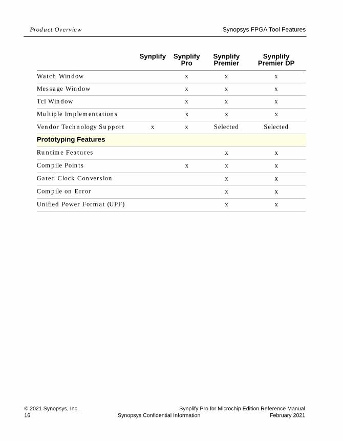
Synopsys FPGA Tool FeaturesThis table distinguishes between major functionality for the Synopsys FPGA products.
Synplify Synplify Pro
Synplify Premier
Synplify Premier DP
Performance
Behavior Extracting Synthesis Technology® (BEST™)
x x x x
Vendor-Generated Core/IP Support (certain technologies)
x x x
FSM Compiler x x x x
FSM Explorer x x x
Gated Clock Conversion x x x
Register Pipelining x x x
Register Retiming x x x
SCOPE® Constraint Entry x x x x
High Reliability Features Limited x x
Integrated Place-and-Route x x x x
Analysis
HDL Analyst® Option x x x
Timing Analyzer - Point-to-point
x x x
Timing Report View x x
FSM Viewer x x x
Crossprobing x x x
Probe Point Creation x x x
Identify® Instrumentor x x x x
Identify Debugger x x x x

Synopsys FPGA Tool Features Product Overview
Synplify Pro for Microchip Edition Reference Manual © 2021 Synopsys, Inc.February 2021 Synopsys Confidential Information 15
Physical Design
Design Planner x
Logic Assignment to Regions x
Area Estimation and Region Capacity
x
Pin Assignment x
Physical Optimizations x x
Physical Analyst x x
Synopsys DesignWare® Foundation Library
x x
Runtime
Hierarchical Design x x x
Multiprocessing /Distributed Processing
x x
Compile on Error x x
Team Design
Mixed Language Design x x x
Compile Points x x x
Hierarchical Design x x x
True Batch Mode (Floating licenses only)
x x x
GUI Batch Mode (Floating licenses)
x x x x
Batch Mode P&R - x x x
Back Annotation of P&R Data - - x x
Identify Integration Limited x x x
Design Environment
Text Editor View x x x x
Synplify Synplify Pro
Synplify Premier
Synplify Premier DP
LO
Product Overview Synopsys FPGA Tool Features
© 2021 Synopsys, Inc. Synplify Pro for Microchip Edition Reference Manual16 Synopsys Confidential Information February 2021
Watch Window x x x
Message Window x x x
Tcl Window x x x
Multiple Implementations x x x
Vendor Technology Support x x Selected Selected
Prototyping Features
Runtime Features x x
Compile Points x x x
Gated Clock Conversion x x
Compile on Error x x
Unified Power Format (UPF) x x
Synplify Synplify Pro
Synplify Premier
Synplify Premier DP

Graphic User Interface Product Overview
Synplify Pro for Microchip Edition Reference Manual © 2021 Synopsys, Inc.February 2021 Synopsys Confidential Information 17
Graphic User InterfaceThe Synopsys FPGA family of products share a common graphical user interface (GUI) in order to ensure a cohesive look and feel across the different products.
LO
Product Overview Graphic User Interface
© 2021 Synopsys, Inc. Synplify Pro for Microchip Edition Reference Manual18 Synopsys Confidential Information February 2021
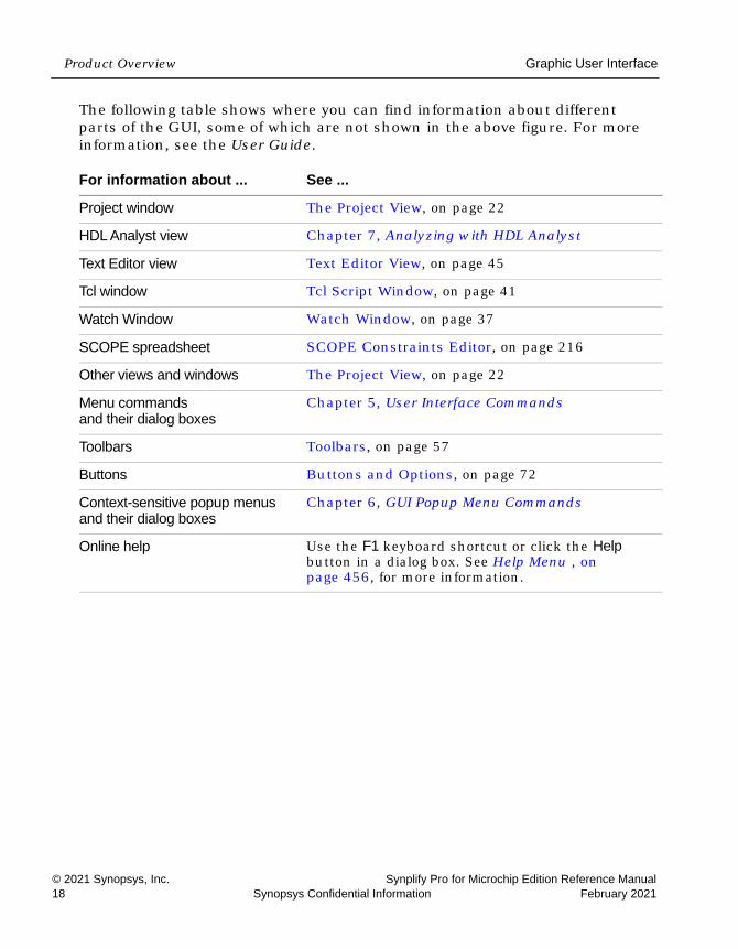
The following table shows where you can find information about different parts of the GUI, some of which are not shown in the above figure. For more information, see the User Guide.
For information about ... See ...
Project window The Project View, on page 22
HDL Analyst view Chapter 7, Analyzing with HDL Analyst
Text Editor view Text Editor View, on page 45
Tcl window Tcl Script Window, on page 41
Watch Window Watch Window, on page 37
SCOPE spreadsheet SCOPE Constraints Editor, on page 216
Other views and windows The Project View, on page 22
Menu commands and their dialog boxes
Chapter 5, User Interface Commands
Toolbars Toolbars, on page 57
Buttons Buttons and Options, on page 72
Context-sensitive popup menus and their dialog boxes
Chapter 6, GUI Popup Menu Commands
Online help Use the F1 keyboard shortcut or click the Help button in a dialog box. See Help Menu , on page 456, for more information.

Getting Help Product Overview
Synplify Pro for Microchip Edition Reference Manual © 2021 Synopsys, Inc.February 2021 Synopsys Confidential Information 19
Getting HelpLook through the documentation for information. You can access the infor-mation online from the Help menu, or refer to the corresponding manual. The following table shows you how the information is organized.
Finding Information
Document SetThis document is part of a series of books included with the Synopsys FPGA synthesis software tool. The set consists of the following books that are packaged with the tool:
• FPGA Synthesis User Guide
• FPGA Synthesis Reference
• FPGA Synthesis Command Reference
• FPGA Synthesis Attributes and Directives Reference
For help with ... Refer to the ...
How to... User Guide
Flow information User Guide
FPGA Implementation Tool
Synopsys Web Page (Web->FPGA Implementation Tools menu command from within the software)
Synthesis features User Guide and Reference Manual
Language and syntax Language Support Reference Manual
Attributes and directives
Attribute Reference Manual
Tcl language Online help (Help->Tcl Help)
Synthesis Tcl commands
Command Reference Manual or type help followed by the command name in the Tcl window
Using tool-specific features and attributes
User Guide
Error and warning messages
Click the message ID code

LO
Product Overview Getting Help
© 2021 Synopsys, Inc. Synplify Pro for Microchip Edition Reference Manual20 Synopsys Confidential Information February 2021
• FPGA Synthesis Language Support Reference
• Identify Instrumentor User Guide
• Identify Debugger User Guide
• Identify Debugging Environment Reference Manual
Synplify Pro for Microchip Edition Reference Manual © 2021 Synopsys, Inc.February 2021 Synopsys Confidential Information 21
C H A P T E R 2
User Interface Overview
This chapter presents tools and technologies that are built into the Synopsys FPGA synthesis software to enhance your productivity.
This chapter describes the following aspects of the graphical user interface (GUI):
• The Project View, on page 22
• The Project Results View, on page 26
• Other Windows and Views, on page 36
• Using the Mouse, on page 52
• Toolbars, on page 57
• Keyboard Shortcuts, on page 64
• Buttons and Options, on page 72

LO
User Interface Overview The Project View
© 2021 Synopsys, Inc. Synplify Pro for Microchip Edition Reference Manual22 Synopsys Confidential Information February 2021
The Project ViewThe Project View is the main interface to the tool. The Project View consists of a Project Management View on the left and a Project Results View on the right. The interface and available functionality vary for your tool. See the following for an overview:
• Multiple Pane Project View, on page 22
Multiple Pane Project ViewThe Project Management view is on the left side of the window, and is used to create or open projects, create new implementations, set device options, and initiate design synthesis. The Project Results view is on the right.
You can also use the Project Management view to manage and synthesize hierarchical designs.
The following figure shows the main parts of the interface. Additional details about the project view are described here:
• Project Management View, on page 24
• The Project Results View

The Project View User Interface Overview
Synplify Pro for Microchip Edition Reference Manual © 2021 Synopsys, Inc.February 2021 Synopsys Confidential Information 23

LO
User Interface Overview The Project View
© 2021 Synopsys, Inc. Synplify Pro for Microchip Edition Reference Manual24 Synopsys Confidential Information February 2021
The Project view has the following main parts:
Project Management View
The Project Management view is on the left side of the window, and is used to create or open projects, create new implementations, set device options, and initiate design synthesis. The graphical user interface (GUI) lets you manage
Project View Interface Description
Status Displays the tool name or the current status of the synthesis job that is running. Clicking in this area displays additional information about the current job.
Buttons and options Allow immediate access to some of the more common commands. See Buttons and Options , on page 72 for details.
Implementation Results view
Lists the result of the synthesis runs for the implementations of your design. You can only view one set of implementation results at a time. Click an implementation in the Project view to make it active and view its result files. The Project Results view includes the following:• Project Status Tab—provides an overview of the project
settings and at-a-glance summary of synthesis messages and reports.
• Implementation Directory—lists the names and types of the result files, and the dates they were last modified.
• Process View—gives you instant visibility to the synthesis and place-and-route job flows.
See The Project Results View , on page 26 for more information.

The Project View User Interface Overview
Synplify Pro for Microchip Edition Reference Manual © 2021 Synopsys, Inc.February 2021 Synopsys Confidential Information 25
hierarchical designs that can be synthesized independently and imported back to the top-level project in a team design flow. The following figure shows the Project view as it appears in the interface.

LO
User Interface Overview The Project Results View
© 2021 Synopsys, Inc. Synplify Pro for Microchip Edition Reference Manual26 Synopsys Confidential Information February 2021
The Project Results ViewThe Project Results view appears on the right side of the Project view and contains the results of the synthesis runs for the implementations of your design. The Project Results view includes the following:
• Project Status Tab
• Implementation Directory
• Process View
• Report Tab
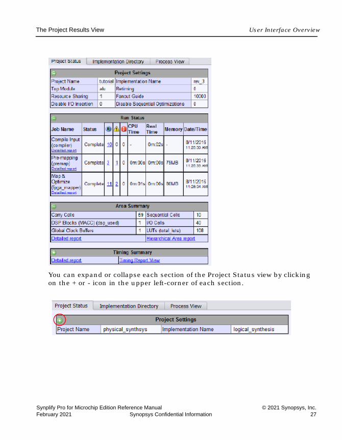
Project Status TabThe Project Status view provides an overview of the project settings and at-a-glance summary of synthesis messages and reports such as an area or optimization summary for the active implementation. You can track the status and settings for your design and easily navigate to reports and messages in the Project view.
To display this window, click the Project Status tab in the Project view. An overview for the project is displayed in a spreadsheet format for each of the following sections:
• Project Settings
• Run Status
• Reports
For details about how to access synthesis results, see Accessing Specific Reports Quickly, on page 193.
The Project Results View User Interface Overview
Synplify Pro for Microchip Edition Reference Manual © 2021 Synopsys, Inc.February 2021 Synopsys Confidential Information 27
You can expand or collapse each section of the Project Status view by clicking on the + or - icon in the upper left-corner of each section.
LO
User Interface Overview The Project Results View
© 2021 Synopsys, Inc. Synplify Pro for Microchip Edition Reference Manual28 Synopsys Confidential Information February 2021
Project SettingsProject Settings is populated with the project settings from the run_options.txt file after a synthesis run. This section displays information, like the following:
• Project name, top-level module, and implementation name
• Project options currently specified, such as Resource Sharing, Fanout Guide, and Disable I/O Insertion
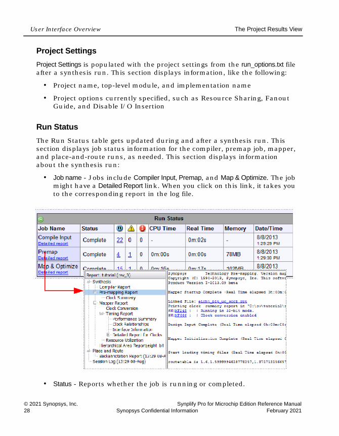
Run StatusThe Run Status table gets updated during and after a synthesis run. This section displays job status information for the compiler, premap job, mapper, and place-and-route runs, as needed. This section displays information about the synthesis run:
• Job name - Jobs include Compiler Input, Premap, and Map & Optimize. The job might have a Detailed Report link. When you click on this link, it takes you to the corresponding report in the log file.
• Status - Reports whether the job is running or completed.

The Project Results View User Interface Overview
Synplify Pro for Microchip Edition Reference Manual © 2021 Synopsys, Inc.February 2021 Synopsys Confidential Information 29
• Notes, Warnings, and Errors - These columns are headed by the respective icons and display the number of messages. The messages themselves are displayed in the Messages tab, beside the TCL Script tab. Links are available to the error message and the log location.
The message numbers may not match for designs with compile points. The numbers reflect the top-level design.
• Real and CPU times, peak memory, and a timestamp
ReportsThe mapper summary table generates various reports such as an
• Area Summary
• Optimization Summary
• Compile Point Summary
Click the Detailed Report link when applicable, to go to the log file and informa-tion about the selected report. These reports are written to the synlog folder for the active implementation.
Area SummaryFor example, the Area Summary contains a resource usage count for compo-nents such as registers, LUTs, and I/O ports in the design. Click the Detailed report link to display the usage count information in the design for this report.
LO
User Interface Overview The Project Results View
© 2021 Synopsys, Inc. Synplify Pro for Microchip Edition Reference Manual30 Synopsys Confidential Information February 2021
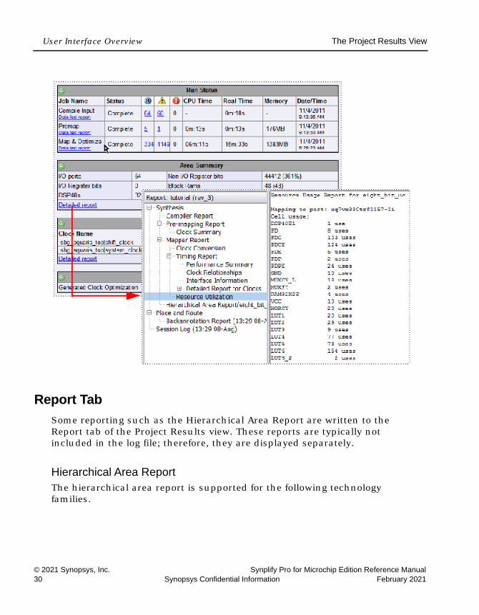
Report TabSome reporting such as the Hierarchical Area Report are written to the Report tab of the Project Results view. These reports are typically not included in the log file; therefore, they are displayed separately.
Hierarchical Area ReportThe hierarchical area report is supported for the following technology families.
The Project Results View User Interface Overview
Synplify Pro for Microchip Edition Reference Manual © 2021 Synopsys, Inc.February 2021 Synopsys Confidential Information 31
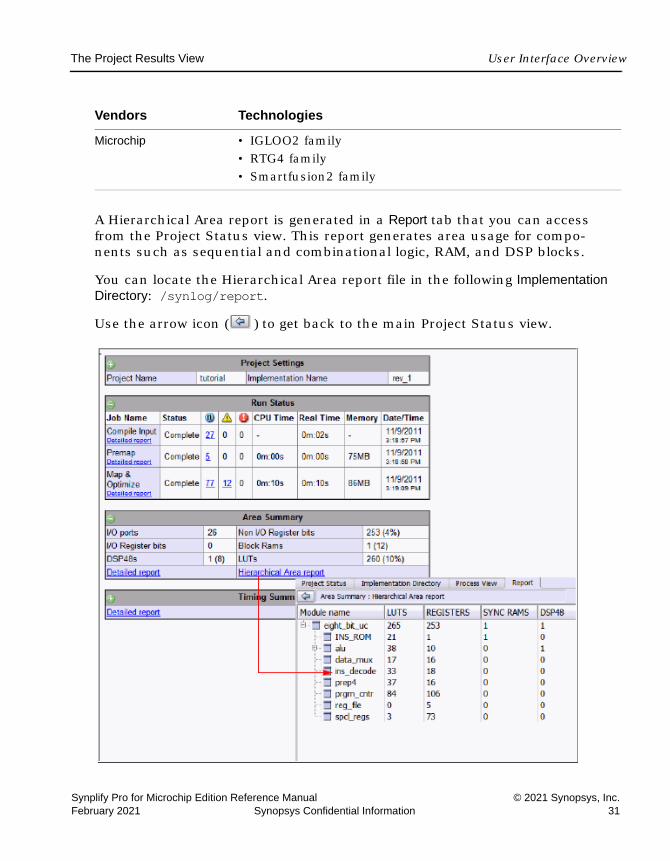
A Hierarchical Area report is generated in a Report tab that you can access from the Project Status view. This report generates area usage for compo-nents such as sequential and combinational logic, RAM, and DSP blocks.
You can locate the Hierarchical Area report file in the following Implementation Directory: /synlog/report.Use the arrow icon ( ) to get back to the main Project Status view.
Vendors Technologies
Microchip • IGLOO2 family• RTG4 family• Smartfusion2 family

LO
User Interface Overview The Project Results View
© 2021 Synopsys, Inc. Synplify Pro for Microchip Edition Reference Manual32 Synopsys Confidential Information February 2021
Implementation DirectoryAn implementation is one version of a project, run with certain parameter or option settings. You can synthesize again, with a different set of options, to get a different implementation. In the Project view, an implementation is shown in the folder of its project; the active implementation is highlighted. You can display multiple implementations in the same Project view. The output files generated for the active implementation are displayed in the Implementation Directory.
The Project Results View User Interface Overview
Synplify Pro for Microchip Edition Reference Manual © 2021 Synopsys, Inc.February 2021 Synopsys Confidential Information 33
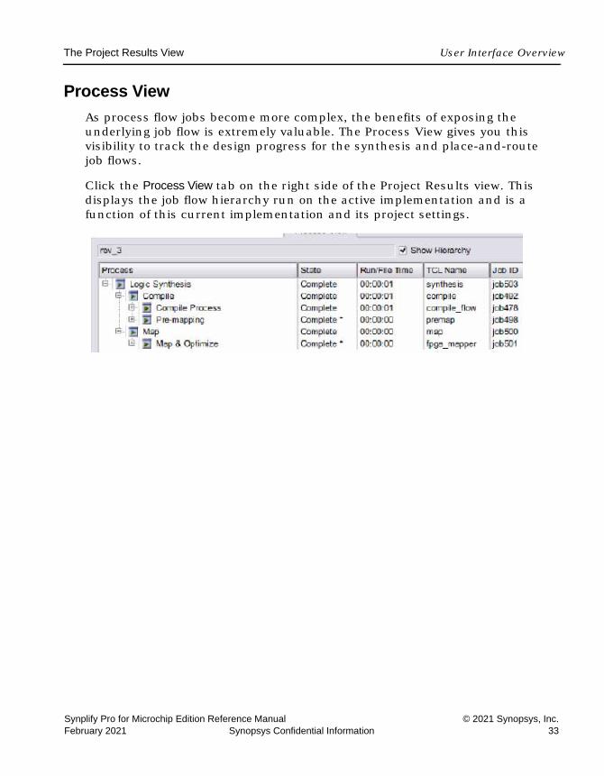
Process ViewAs process flow jobs become more complex, the benefits of exposing the underlying job flow is extremely valuable. The Process View gives you this visibility to track the design progress for the synthesis and place-and-route job flows.
Click the Process View tab on the right side of the Project Results view. This displays the job flow hierarchy run on the active implementation and is a function of this current implementation and its project settings.
LO
User Interface Overview The Project Results View
© 2021 Synopsys, Inc. Synplify Pro for Microchip Edition Reference Manual34 Synopsys Confidential Information February 2021
Process View Displays and ControlsThe Process View shows the current state of a job and allows you to control the run. You can see various aspects of the synthesis process flow, such as logical synthesis, premap, and map. If you run place and route, you can see its job processes as well.
Appropriate jobs of the process flow contains the following information:
• Job Input and Output Files
• Completion State
Displays if the job generated an error, warning, or was canceled.
• Job State
– Out-of-date - Job needs to be run.
– Running - Job is active.
– Complete - Job has completed and is up-to-date.
– Complete * - Job is up-to-date, so the job is skipped.
• Run/File Time - Job process flow runtime in real time or file creation date timestamp.
• Job TCL Command - Job process name.
Each job has the following control commands that allows you to run jobs at any stage of the design process, for example map. Right-click on any job icon and select one of the following commands from the popup menu:
• Cancel jobProcess that is running
• Disable jobProcess that you do not want to run
• Run this jobProcess only
• Run to this jobProcess from the beginning of run
• Run from this jobProcess to the end of run

The Project Results View User Interface Overview
Synplify Pro for Microchip Edition Reference Manual © 2021 Synopsys, Inc.February 2021 Synopsys Confidential Information 35
Hierarchical Job FlowsA hierarchical job flow runs two or more subordinate jobs. Primitive jobs launch an executable, but have no subordinate jobs. The Logical Synthesis flow is a hierarchical job that runs the Compile and Map flows.
The state of a hierarchical job depends on the state of its subordinate jobs.
• If a subordinate job is out-of-date, then its parent job is out-of-date.
• If a subordinate job has an error, then its parent job terminates with this error.
• If a subordinate job has been canceled, then its parent job is canceled as well.
• If a subordinate job is running, then its parent job is also running.
The Process View is a hierarchical tree view. To collapse or expand the main hierarchical tree, enable or disable the Show Hierarchy option. Use the plus or minus icon to expand or collapse each process flow to show the details of the jobs. The icons below are used to show the information for the state of each process:
• Red arrow ( ) - Job is out-of-date and needs to be rerun.
• Green arrow ( ) - Job is up-to-date.
• Red Circle with! ( ) - Job encountered an error.

LO
User Interface Overview Other Windows and Views
© 2021 Synopsys, Inc. Synplify Pro for Microchip Edition Reference Manual36 Synopsys Confidential Information February 2021
Other Windows and ViewsBesides the Project view, the tool provides other windows and views that help you manage input and output files, direct the synthesis process, and analyze your design and its results. The following windows and views are described here:
• Dockable GUI Entities, on page 37
• Watch Window, on page 37
• Tcl Script and Messages Windows, on page 40
• Tcl Script Window, on page 41
• Message Viewer, on page 41
• Output Windows (Tcl Script and Watch Windows), on page 45
• Text Editor View, on page 45
• Context Help Editor Window, on page 48
• Interactive Attribute Examples, on page 50
See the following for descriptions of other views and windows that are not covered here:
Project View The Project View, on page 22
SCOPE Interface SCOPE Tabs, on page 217
HDL Analyst Schematic Chapter 7, Analyzing with HDL Analyst

Other Windows and Views User Interface Overview
Synplify Pro for Microchip Edition Reference Manual © 2021 Synopsys, Inc.February 2021 Synopsys Confidential Information 37
Dockable GUI EntitiesSome of the main GUI entities can appear as either independent windows or docked elements of the main application window. These entities include the menu bar, Watch window, Tcl window, and various toolbars (see the descrip-tion of each entity for details). Docked elements function effectively as panes of the application window; you can drag the border between two such panes to adjust their relative areas.
Watch WindowThe Watch window displays selected information from the log file (see Log File, on page 157) as a spreadsheet of parameters that you select to monitor. The values are updated when synthesis finishes.
Watch Window DisplayDisplay of the Watch window is controlled by the View ->Watch Window command. By default, the Watch window is below the Project view in the lower right corner of the main application window.
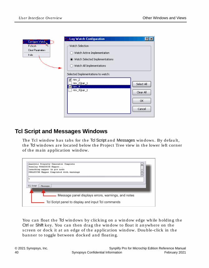
To access the Watch window configuration menu, right-click in any cell. Select Configure Watch to display the Log Watch Configuration dialog box.
In the Watch window, indicate which implementations to watch under Watch Selection. The selected implementation(s) will display in the Watch window.

LO
User Interface Overview Other Windows and Views
© 2021 Synopsys, Inc. Synplify Pro for Microchip Edition Reference Manual38 Synopsys Confidential Information February 2021
You can move the Watch window anywhere on the screen; you can make it float in its own window (named Watch Window) or dock it at a docking area (an edge) of the application window. Double-click in the banner to toggle between docked and floating.
The Watch window has a special positioning popup menu that you access by right-clicking the window border. The following commands are in the menu:
Right-clicking the window title bar when the Watch window is floating displays an alternative popup menu with commands Hide and Move; Move lets you position the window using either the arrow keys or the mouse.
Using the Watch WindowYou can view and compare the results of multiple implementations in the Watch window.
Command Description
Allow Docking A toggle: when enabled, the window can be docked.
Hide Hides the window; use View ->Watch Window to show it again.
Float in Main Window A toggle: when enabled, the window is floated (undocked).

Other Windows and Views User Interface Overview
Synplify Pro for Microchip Edition Reference Manual © 2021 Synopsys, Inc.February 2021 Synopsys Confidential Information 39
To choose log parameters from a pull-down menu, click in the Log Parameter section of the window. Click the pull-down arrow that appears to display the parameter list choices:
The Watch window creates an entry for each implementation of a project:
To choose the implementations to watch, use the Log Watch Configuration dialog box. To display this box, right-click in the Watch window, then choose Configure Watch in the popup menu. Enable Watch Selected Implementations, then choose the implementations you want to watch in the list Selected Implementa-tions to watch. The other buttons let you watch only the active implementation or all implementations.
LO
User Interface Overview Other Windows and Views
© 2021 Synopsys, Inc. Synplify Pro for Microchip Edition Reference Manual40 Synopsys Confidential Information February 2021
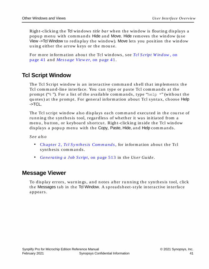
Tcl Script and Messages WindowsThe Tcl window has tabs for the Tcl Script and Messages windows. By default, the Tcl windows are located below the Project Tree view in the lower left corner of the main application window.
You can float the Tcl windows by clicking on a window edge while holding the Ctrl or Shift key. You can then drag the window to float it anywhere on the screen or dock it at an edge of the application window. Double-click in the banner to toggle between docked and floating.
Other Windows and Views User Interface Overview
Synplify Pro for Microchip Edition Reference Manual © 2021 Synopsys, Inc.February 2021 Synopsys Confidential Information 41
Right-clicking the Tcl windows title bar when the window is floating displays a popup menu with commands Hide and Move. Hide removes the window (use View ->Tcl Window to redisplay the window). Move lets you position the window using either the arrow keys or the mouse.
For more information about the Tcl windows, see Tcl Script Window, on page 41 and Message Viewer, on page 41.
Tcl Script WindowThe Tcl Script window is an interactive command shell that implements the Tcl command-line interface. You can type or paste Tcl commands at the prompt (“% ”). For a list of the available commands, type “help *” (without the quotes) at the prompt. For general information about Tcl syntax, choose Help ->TCL.
The Tcl script window also displays each command executed in the course of running the synthesis tool, regardless of whether it was initiated from a menu, button, or keyboard shortcut. Right-clicking inside the Tcl window displays a popup menu with the Copy, Paste, Hide, and Help commands.
See also
• Chapter 2, Tcl Synthesis Commands, for information about the Tcl synthesis commands.
• Generating a Job Script, on page 513 in the User Guide.
Message ViewerTo display errors, warnings, and notes after running the synthesis tool, click the Messages tab in the Tcl Window. A spreadsheet-style interactive interface appears.

LO
User Interface Overview Other Windows and Views
© 2021 Synopsys, Inc. Synplify Pro for Microchip Edition Reference Manual42 Synopsys Confidential Information February 2021
Interactive tasks in the Messages panel include:
• Drag the pane divider with the mouse to change the relative column size.
• Click on the ID entry to open online help for the error, warning, or note.
• Click on a Source Location entry to go to the section of code in the source HDL file that is causing the message.
• Click on a Log Location entry to go to its location in the log file.
The following table describes the contents of the Messages panel. You can sort the messages by clicking the column headers. For further sorting, use Find and Filter. For details about using this window, see Checking Results in the Message Viewer, on page 205 in the User Guide.
Item Description
Find Type into this field to find errors, warnings, or notes.
Filter Opens the Warning Filter dialog box. See Messages Filter , on page 44.
Apply Filter Enable/disable the last saved filter.

Other Windows and Views User Interface Overview
Synplify Pro for Microchip Edition Reference Manual © 2021 Synopsys, Inc.February 2021 Synopsys Confidential Information 43
Group Common ID’s
Enable/disable grouping of repeated messages. Groups are indicated by a number next to the type icon. There are two types of groups:• The same warning or note ID appears in multiple source files
indicated by a dash in the source files column.• Multiple warnings or notes in the same line of source code
indicated by a bracketed number.
Type The icons indicate the type of message: ErrorWarningNoteAdvisory
A plus sign next to an icon indicates that repeated messages are grouped together. Click the plus sign to expand and view the various occurrences of the message.
ID This is the message ID. You can select an underlined ID to launch help on the message.
Message The error, warning, or note message text.
Source Location The HDL source file that generated the error, warning, or note message.
Log Location The location of the error, warning, or note message in the log file.
Time The time that the error, warning, or note message was recorded in the log file for the various stages of synthesis (for example: compiler, premap, and map). If you rerun synthesis, only new messages generate a new timestamp for this session. Note: Once synthesis has run to completion, all the .srr files for the different stages of synthesis are merged into one unified .srr file. If you exit the GUI, these timestamps remain the same when you re-open the same project in the GUI again.
Report Indicates which section of the Log File report the error appears, for example Compiler or Mapper.
Item Description

LO
User Interface Overview Other Windows and Views
© 2021 Synopsys, Inc. Synplify Pro for Microchip Edition Reference Manual44 Synopsys Confidential Information February 2021
Messages FilterYou filter which errors, warnings, and notes appear in the Messages panel of the Tcl Window using match criteria for each field. The selections are combined to produce the result. You can elect to hide or show the warnings that match the criteria you set. See Checking Results in the Message Viewer, on page 205 in the User Guide.
The following is a filtering example.
Item Description
Hide Filter Matches Hides matched criteria in the Messages Panel.
Show Filter Matches Shows matched criteria in the Messages Panel.
Syntax Help Gives quick syntax descriptions.
Apply Applies the filter criteria to the Messages Panel report, without closing the window.
Type, ID, Message, Source Location, Log Location, Time, Report
Log file report criteria to use when filtering.
Other Windows and Views User Interface Overview
Synplify Pro for Microchip Edition Reference Manual © 2021 Synopsys, Inc.February 2021 Synopsys Confidential Information 45
Output Windows (Tcl Script and Watch Windows)The Output windows are the Tcl Script and Log Watch windows. To display or hide them, use View->Output Windows from the main menu. Refer to Watch Window, on page 37 and Tcl Script and Messages Windows, on page 40 for more information.
Text Editor ViewThe Text Editor view displays text files. These can be constraint files, source code files, or other informational or report files. You can enter and edit text in the window. You use this window to update source code and fix syntax or synthesis errors. You can also use it to crossprobe the design. For informa-tion about using the Text Editor, see Editing HDL Source Files with the Built-in Text Editor, on page 39 in the User Guide.
LO
User Interface Overview Other Windows and Views
© 2021 Synopsys, Inc. Synplify Pro for Microchip Edition Reference Manual46 Synopsys Confidential Information February 2021
Opening the Text EditorTo open the Text Editor to edit an existing file, do one of the following:
• Double-click a source code file (.v or .vhd) in the Project view.
• Choose File ->Open. In the dialog box displayed, double-click a file to open it.
With the Microsoft® Windows® operating system, you can instead drag and drop a source file from a Windows folder into the gray background area of the GUI (not into any particular view).
To open the Text Editor on a new file, do one of the following:
• Choose File ->New, then specify the kind of text file you want to create.
• Click the HDL icon ( ) to create and edit an HDL source file.
The Text Editor colors HDL source code keywords such as module and output blue and comments green.
Other Windows and Views User Interface Overview
Synplify Pro for Microchip Edition Reference Manual © 2021 Synopsys, Inc.February 2021 Synopsys Confidential Information 47
Text Editor FeaturesThe Text Editor has the features listed in the following table.
Feature Description
Color coding Keywords are blue, comments green, and strings red. All other text is black.
Editing text You can use the Edit menu or keyboard shortcuts for basic editing operations like Cut, Copy, Paste, Find, Replace, and Goto.
Completing keywords To complete a keyword, type enough characters to make the string unique and then press the Esc key.
Indenting a block of text The Tab key indents a selected block of text to the right. Shift-Tab indents text to the left.
Inserting a bookmark Click the line you want to bookmark. Choose Edit ->Toggle Bookmark, type Ctrl-F2, or click the Toggle Bookmark icon ( ) on the Edit toolbar. The line number is highlighted to indicate that there is a bookmark at the beginning of the line.
Deleting a bookmark Click the line with the bookmark. Choose Edit ->Toggle Bookmark, type Ctrl-F2, or click the Toggle Bookmark icon ( ) on the Edit toolbar.
Deleting all bookmarks Choose Edit ->Delete all Bookmarks, type Ctrl-Shift-F2, or click the Clear All Bookmarks icon ( ) on the Edit toolbar.
Editing columns Press and hold Alt, then drag the mouse down a column of text to select it.
Commenting out code Choose Edit ->Advanced ->Comment Code. The rest of the current line is commented out: the appropriate comment prefix is inserted at the current text cursor position.
Checking syntax Use Run ->Syntax Check to highlight syntax errors, such as incorrect keywords and punctuation, in source code. If the active window shows an HDL file, then only that file is checked. Otherwise, the entire project is checked.
Checking synthesis Use Run ->Synthesis Check to highlight hardware-related errors in source code, like incorrectly coded flip-flops. If the active window shows an HDL file, then only that file is checked. Otherwise, the entire project is checked.
LO
User Interface Overview Other Windows and Views
© 2021 Synopsys, Inc. Synplify Pro for Microchip Edition Reference Manual48 Synopsys Confidential Information February 2021
See also:
• Editor Options Command, on page 437, for information on setting Text Editor preferences.
• File Menu, on page 306, for information on printing setup operations.
• Edit Menu Commands for the Text Editor, on page 312, for information on Text Editor editing commands.
• Text Editor Popup Menu, on page 461, for information on the Text Editor popup menu.
• Text Editor Toolbar, on page 61, for information on bookmark icons of the Edit toolbar.
• Keyboard Shortcuts, on page 64, for information on keyboard shortcuts that can be used in the Text Editor.
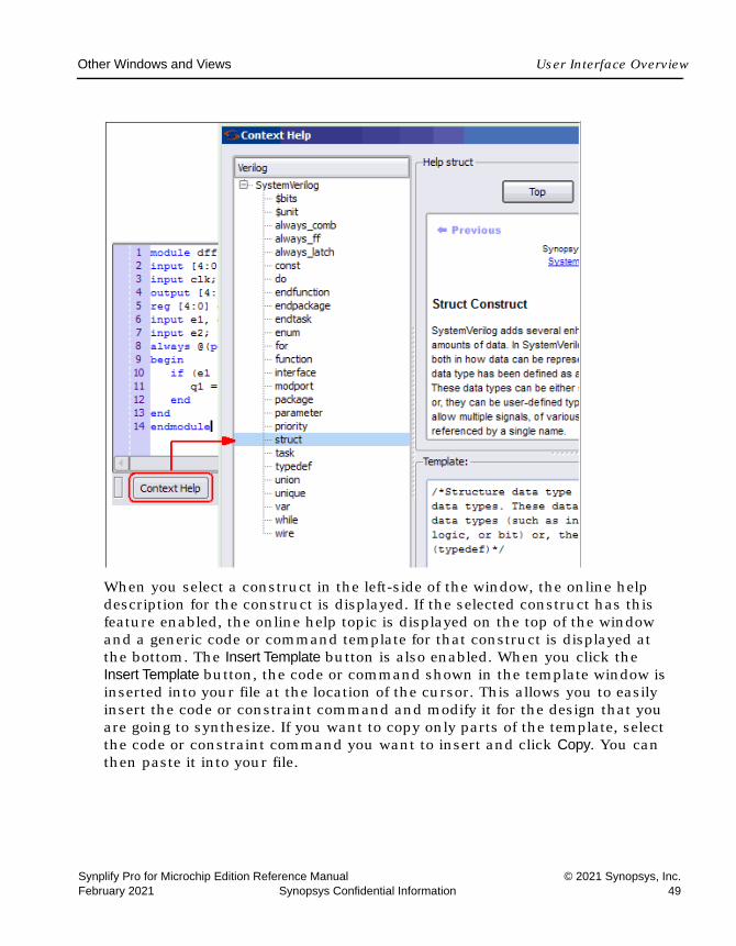
Context Help Editor WindowUse the Context Help button to copy Verilog, SystemVerilog, or VHDL constructs into your source file or Tcl constraint commands into your Tcl file. When you load a Verilog/SystemVerilog/VHDL file or Tcl file into the UI, the Context Help button displays at the bottom of the window. Click on this button to display the Context Help Editor.
Other Windows and Views User Interface Overview
Synplify Pro for Microchip Edition Reference Manual © 2021 Synopsys, Inc.February 2021 Synopsys Confidential Information 49
When you select a construct in the left-side of the window, the online help description for the construct is displayed. If the selected construct has this feature enabled, the online help topic is displayed on the top of the window and a generic code or command template for that construct is displayed at the bottom. The Insert Template button is also enabled. When you click the Insert Template button, the code or command shown in the template window is inserted into your file at the location of the cursor. This allows you to easily insert the code or constraint command and modify it for the design that you are going to synthesize. If you want to copy only parts of the template, select the code or constraint command you want to insert and click Copy. You can then paste it into your file.
LO
User Interface Overview Other Windows and Views
© 2021 Synopsys, Inc. Synplify Pro for Microchip Edition Reference Manual50 Synopsys Confidential Information February 2021
Interactive Attribute ExamplesThe Interactive Attribute Examples wizard lets you select pre-defined attri-butes to run in a project. To use this tool:
1. Launch the wizard from Help->Demos & Examples.
2. Click the Examples button. Then click on Interactive Attribute Examples and the Launch Interactive Attributes Wizard links.
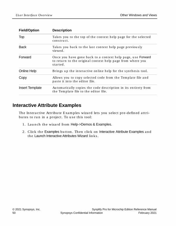
Field/Option Description
Top Takes you to the top of the context help page for the selected construct.
Back Takes you back to the last context help page previously viewed.
Forward Once you have gone back to a context help page, use Forward to return to the original context help page from where you started.
Online Help Brings up the interactive online help for the synthesis tool.
Copy Allows you to copy selected code from the Template file and paste it into the editor file.
Insert Template Automatically copies the code description in its entirety from the Template file to the editor file.

Other Windows and Views User Interface Overview
Synplify Pro for Microchip Edition Reference Manual © 2021 Synopsys, Inc.February 2021 Synopsys Confidential Information 51
3. Double-click on an attribute to start the wizard.
4. Specify the Working Directory location to write your project.
5. Click Generate to generate a project for your attribute.
A project will be created with an implementation for each attribute value selected.
6. Click Generate Run to run synthesis for all the implementations. When synthesis completes:
– The Technology view opens to show how the selected attribute impacts synthesis.
– You can compare resource utilization and timing information between implementations in the Log Watch window.
LO
User Interface Overview Using the Mouse
© 2021 Synopsys, Inc. Synplify Pro for Microchip Edition Reference Manual52 Synopsys Confidential Information February 2021
Using the MouseThe mouse button operations in Synopsys FPGA product is standard; refer to Mouse Operation Terminology for a summary of supported functions. The tool provides support for:
• Using Mouse Strokes, on page 53
• Using the Mouse Buttons, on page 54
• Using the Mouse Wheel, on page 56
Mouse Operation TerminologyThe following terminology is used to refer to mouse operations:
Term Meaning
Click Click with the left mouse button: press then release it without moving the mouse.
Double-click Click the left mouse button twice rapidly, without moving the mouse.
Right-click Click with the right mouse button.
Drag Press the left mouse button, hold it down while moving the mouse, then release it. Dragging an object moves the object to where the mouse is released; then, releasing is sometimes called “dropping”. Dragging initiated when the mouse is not over an object often traces a selection rectangle, whose diagonal corners are at the press and release positions.
Press Depress a mouse button; unless otherwise indicated, the left button is implied. It is sometimes used as an abbreviation for “press and hold”.
Hold Keep a mouse button depressed. It is sometimes used as an abbreviation for “press and hold”.
Release Stop holding a mouse button depressed.

Using the Mouse User Interface Overview
Synplify Pro for Microchip Edition Reference Manual © 2021 Synopsys, Inc.February 2021 Synopsys Confidential Information 53
Using Mouse StrokesMouse strokes are used to quickly perform simple repetitive commands. Mouse strokes are drawn by pressing and holding the right mouse button as you draw the pattern. The stroke must be at least 16 pixels in width or height to be recognized. You will see a green mouse trail as you draw the stroke (the actual color depends on the window background color).
Some strokes are context sensitive. That is, the interpretation of the stroke depends upon the window in which the stroke is started. For example, in an HDL Analyst view, the right stroke means “Next Sheet.” In a dialog box, the right stroke means “OK.”
For information on each of the available mouse strokes, consult the Mouse Stroke Tutor.
The strokes you draw are interpreted on a grid of one to three rows. Some strokes are similar, differing only in the number of columns or rows, so it may take a little practice to draw them correctly. For example, the strokes for Redo and Back differ in that the Redo stroke is back and forth horizontally, within a single-row grid, while the Back stroke involves vertical movement as well.
The Mouse Stroke TutorDo one of the following to access the Mouse Stroke Tutor:
• Help->Stroke Tutor
• Draw a question mark stroke ("?")
• Scribble (Show tutor when scribbling must be enabled on the Stroke Help dialog box)
Redo Last Operation Back to Previous View

LO
User Interface Overview Using the Mouse
© 2021 Synopsys, Inc. Synplify Pro for Microchip Edition Reference Manual54 Synopsys Confidential Information February 2021
The tutor displays the available strokes along with a description and a diagram of the stroke. You can draw strokes while the tutor is displayed.
Mouse strokes are context sensitive. When viewing the Stroke Tutor, you can choose All Strokes or Current Context to view just the strokes that apply to the context of where you invoked the tutor. For example, if you draw the "?" stroke in an HDL Analyst window, the Current Context option in the tutor shows only those strokes recognized in the HDL Analyst window.
You can display the tutor while working in a window such as the HDL Analyst view. However you cannot display the tutor while a modal dialog is displayed, as input is restricted to the modal dialog.
Using the Mouse ButtonsThe operations you can perform using mouse buttons include the following:
• You select an object by clicking it. You deselect a selected object by clicking it. Selecting an object by clicking it deselects all previously selected objects.
• You can select and deselect multiple objects by pressing and holding the Control key (Ctrl) while clicking each of the objects.
Using the Mouse User Interface Overview
Synplify Pro for Microchip Edition Reference Manual © 2021 Synopsys, Inc.February 2021 Synopsys Confidential Information 55
• You can select a range of objects in a Hierarchy Browser, as follows:
– select the first object in the range
– scroll the tree of objects, if necessary, to display the last object in the range
– press and hold the Shift key while clicking the last object in the range
Selecting a range of objects in a Hierarchy Browser crossprobes to the corresponding schematic, where the same objects are automatically selected.
• You can select all of the objects in a region by tracing a selection rectangle around them (lassoing).
• You can select text by dragging the mouse over it. You can alternatively select text containing no white space (such as spaces) by double-clicking it.
• Double-clicking sometimes selects an object and immediately initiates a default action associated with it. For example, double-clicking a source file in the Project view opens the file in a Text Editor window.
• You can access a contextual popup menu by clicking the right mouse button. The menu displayed is specific to the current context, including the object or window under the mouse.
For example, right-clicking a project name in the Project view displays a popup menu with operations appropriate to the project file. Right-clicking a source (HDL) file in the Project view displays a popup menu with operations applicable to source files.
Right-clicking a selectable object in an HDL Analyst schematic also selects it, and deselects anything that was selected. The resulting popup menu applies only to the selected object. See Working in the Schematic, on page 224 of the FPGA Synthesis User Guide, for information on HDL Analyst views.
Most of the mouse button operations involve selecting and deselecting objects. To use the mouse in this way in an HDL Analyst schematic, the mouse pointer must be the cross-hairs symbol: . If the cross-hairs pointer is not displayed, right-click the schematic background to display it.
LO
User Interface Overview Using the Mouse
© 2021 Synopsys, Inc. Synplify Pro for Microchip Edition Reference Manual56 Synopsys Confidential Information February 2021
Using the Mouse WheelIf your mouse has a wheel and you are using a Microsoft Windows platform, you can use the wheel to scroll and zoom, as follows:
• Whenever only a horizontal scroll bar is visible, rotating the wheel scrolls the window horizontally.
• Whenever a vertical scroll bar is visible, rotating the wheel scrolls the window vertically.
• Whenever both horizontal and vertical scroll bars are visible, rotating the wheel while pressing and holding the Shift key scrolls the window horizontally.
• In a window that can be zoomed, such as a graphics window, rotating the wheel while pressing and holding the Ctrl key zooms the window.

Toolbars User Interface Overview
Synplify Pro for Microchip Edition Reference Manual © 2021 Synopsys, Inc.February 2021 Synopsys Confidential Information 57
ToolbarsToolbars provide a quick way to access common menu commands by clicking their icons. The following standard toolbars are available:
• Project Toolbar — Project control and file manipulation.
• Analyst Toolbar — Manipulation of compiled and mapped schematic views.
• Text Editor Toolbar — Text editor bookmark commands.
• FSM Viewer Toolbar — Display of finite state machine (FSM) informa-tion.
• Tools Toolbar — Opens supporting tool.
You can enable or disable the display of individual toolbars - see Toolbar Command, on page 328.
By dragging a toolbar, you can move it anywhere on the screen: you can make it float in its own window or dock it at a docking area (an edge) of the application window. To move the menu bar to a docking area without docking it there (that is, to leave it floating), press and hold the Ctrl or Shift key while dragging it.
Right-clicking the window title bar when a toolbar is floating displays a popup menu with commands Hide and Move. Hide removes the window. Move lets you position the window using either the arrow keys or the mouse.
Project ToolbarThe Project toolbar provides the following icons, by default:

LO
User Interface Overview Toolbars
© 2021 Synopsys, Inc. Synplify Pro for Microchip Edition Reference Manual58 Synopsys Confidential Information February 2021
The following table describes the default Project icons. Each is equivalent to a File or Edit menu command; for more information, see the following:
• File Menu, on page 306
• Edit Menu, on page 311
Icon Description
Open Project Displays the Open Project dialog box to create a new project or to open an existing project. Same as File ->Open Project.
New HDL file Opens the Text Editor window with a new, empty source file. Same as File ->New, Verilog File or VHDL File.
New Constraint File (SCOPE) Opens the SCOPE spreadsheet with a new, empty constraint file.Same as File ->New, Constraint File (SCOPE).
Open Displays the Open dialog box, to open a file. Same as File ->Open.
Save Saves the current file. If the file has not yet been saved, this displays the Save As dialog box, where you specify the filename. The kind of file depends on the active view.Same as File ->Save.
Save All Saves all files associated with the current design. Same as File ->Save All.
Cut Cuts text or graphics from the active view, making it available to Paste. Same as Edit ->Cut.
Paste Pastes previously cut or copied text or graphics to the active view. Same as Edit ->Paste.
Toolbars User Interface Overview
Synplify Pro for Microchip Edition Reference Manual © 2021 Synopsys, Inc.February 2021 Synopsys Confidential Information 59
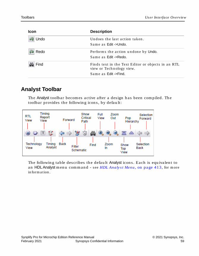
Analyst ToolbarThe Analyst toolbar becomes active after a design has been compiled. The toolbar provides the following icons, by default:
The following table describes the default Analyst icons. Each is equivalent to an HDL Analyst menu command - see HDL Analyst Menu, on page 413, for more information.
Undo Undoes the last action taken. Same as Edit ->Undo.
Redo Performs the action undone by Undo. Same as Edit ->Redo.
Find Finds text in the Text Editor or objects in an RTL view or Technology view. Same as Edit ->Find.
Icon Description

LO
User Interface Overview Toolbars
© 2021 Synopsys, Inc. Synplify Pro for Microchip Edition Reference Manual60 Synopsys Confidential Information February 2021
Icon Description
RTL View Opens a new, hierarchical RTL view: a register transfer-level schematic of the compiled design, together with the associated Hierarchy Browser. Same as HDL Analyst ->RTL ->Hierarchical View.
Technology View Opens a new, hierarchical Technology view: a technology-level schematic of the mapped (synthesized) design, together with the associated Hierarchy Browser. Same as HDL Analyst ->Technology ->Hierarchical View.
Timing Analyst Generates and displays a custom timing report and view. The timing report provides more information than the default report (specific paths or more than five paths) or one that provides timing based on additional analysis constraint files. See Analysis Menu , on page 401. Only available for certain device technologies.Same as Analysis ->Timing Analyst.
Filter Schematic Filters your entire design to show only the selected objects. The result is a filtered schematic. Same as HDL Analyst ->Filter Schematic.
Show Critical Path Filters your design to show only the instances (and their paths) whose slack times are within the slack margin of the worst slack time of the design (see HDL Analyst ->Set Slack Margin). The result is flat if the entire design was already flat.Available only in a Technology view.
Back Goes backward in displaying schematics of the current HDL Analyst view. Same as View ->Back.
Forward Goes forward in displaying schematics of the current HDL Analyst view. Same as View ->Forward.
Zoom In
Zoom Out
Zooms the view in or out. Buttons stay active until deselected.Same as View ->Zoom In or View ->Zoom Out.

Toolbars User Interface Overview
Synplify Pro for Microchip Edition Reference Manual © 2021 Synopsys, Inc.February 2021 Synopsys Confidential Information 61
Text Editor ToolbarThe Edit toolbar is active whenever the Text Editor is active. You use it to edit bookmarks in the file. (Other editing operations are located on the Project toolbar - see Project Toolbar, on page 57.) The Edit toolbar provides the following icons, by default:
The following table describes the default Edit icons. Each is available in the Text Editor, and each is equivalent to an Edit menu command there - see Edit Menu Commands for the Text Editor, on page 312, for more information.
Zoom Full Zoom that reduces the active view to display the entire design.Same as View ->Full View.
Show Top Level Displays the schematic for the top-level view.
Pop Hierarchy Traverses the schematic hierarchy using pop mode.
Selection Back Displays the previous schematic that was selected.
Selection Forward Toggles back to the original schematic that was previously selected.
Icon Description
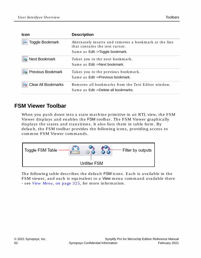
LO
User Interface Overview Toolbars
© 2021 Synopsys, Inc. Synplify Pro for Microchip Edition Reference Manual62 Synopsys Confidential Information February 2021
FSM Viewer ToolbarWhen you push down into a state machine primitive in an RTL view, the FSM Viewer displays and enables the FSM toolbar. The FSM Viewer graphically displays the states and transitions. It also lists them in table form. By default, the FSM toolbar provides the following icons, providing access to common FSM Viewer commands.
The following table describes the default FSM icons. Each is available in the FSM viewer, and each is equivalent to a View menu command available there - see View Menu, on page 325, for more information.
Icon Description
Toggle Bookmark Alternately inserts and removes a bookmark at the line that contains the text cursor. Same as Edit ->Toggle bookmark.
Next Bookmark Takes you to the next bookmark. Same as Edit ->Next bookmark.
Previous Bookmark Takes you to the previous bookmark. Same as Edit ->Previous bookmark.
Clear All Bookmarks Removes all bookmarks from the Text Editor window. Same as Edit ->Delete all bookmarks.

Toolbars User Interface Overview
Synplify Pro for Microchip Edition Reference Manual © 2021 Synopsys, Inc.February 2021 Synopsys Confidential Information 63
Tools ToolbarThe Tools Toolbar opens supporting tool.
Icon Description
Toggle FSM Table Toggles the display of state-and-transition tables. Same as View->FSM Table.
Unfilter FSM Restores a filtered FSM diagram so that all the states and transitions are showing. Same as View->Unfilter.
Filter by outputs Hides all but the selected state(s), their output transitions, and the destination states of those transitions. Same as View->Filter->By output transitions.
Icon Description
Constraint Check Checks the syntax and applicability of the timing constraints in the constraint file for your project and generates a report (project_name_cck.rpt).Same as Run->Constraint Check.
Identify Instrumentor Brings up the Synopsys Identify Instrumentor product. For more information, see Working with the Identify Tools , on page 556of the User Guide.
Launch Identify Debugger Launches the Synopsys Identify Debugger product. For more information, see Working with the Identify Tools , on page 556of the User Guide.
Launch SYNCore Launches the SYNCore IP wizard. This tool helps you build IP blocks such as memory models for your design. For more information, see Launch SYNCore Command , on page 390.
VCS Simulator Configures and launches the VCS simulator.

LO
User Interface Overview Keyboard Shortcuts
© 2021 Synopsys, Inc. Synplify Pro for Microchip Edition Reference Manual64 Synopsys Confidential Information February 2021
Keyboard ShortcutsKeyboard shortcuts are key sequences that you type in order to run a command. Menus list keyboard shortcuts next to the corresponding commands.
For example, to check syntax, you can press and hold the Shift key while you type the F7 key, instead of using the menu command Run ->Syntax Check.
The following table describes the keyboard shortcuts.
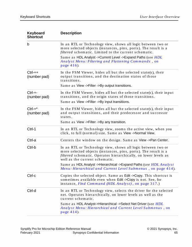
Keyboard Shortcuts User Interface Overview
Synplify Pro for Microchip Edition Reference Manual © 2021 Synopsys, Inc.February 2021 Synopsys Confidential Information 65
Keyboard Shortcut
Description
b In an RTL or Technology view, shows all logic between two or more selected objects (instances, pins, ports). The result is a filtered schematic. Limited to the current schematic. Same as HDL Analyst ->Current Level ->Expand Paths (see HDL Analyst Menu: Filtering and Flattening Commands , on page 416).
Ctrl-++ (number pad)
In the FSM Viewer, hides all but the selected state(s), their output transitions, and the destination states of those transitions.Same as View ->Filter ->By output transitions.
Ctrl-+-(number pad)
In the FSM Viewer, hides all but the selected state(s), their input transitions, and the origin states of those transitions. Same as View ->Filter ->By input transitions.
Ctrl-+*(number pad)
In the FSM Viewer, hides all but the selected state(s), their input and output transitions, and their predecessor and successor states. Same as View ->Filter ->By any transition.
Ctrl-1 In an RTL or Technology view, zooms the active view, when you click, to full (normal) size. Same as View ->Normal View.
Ctrl-a Centers the window on the design. Same as View ->Pan Center.
Ctrl-b In an RTL or Technology view, shows all logic between two or more selected objects (instances, pins, ports). The result is a filtered schematic. Operates hierarchically, on lower levels as well as the current schematic. Same as HDL Analyst ->Hierarchical ->Expand Paths (see HDL Analyst Menu: Hierarchical and Current Level Submenus , on page 414).
Ctrl-c Copies the selected object. Same as Edit ->Copy. This shortcut is sometimes available even when Edit ->Copy is not. See, for instance, Find Command (HDL Analyst) , on page 317.)
Ctrl-d In an RTL or Technology view, selects the driver for the selected net. Operates hierarchically, on lower levels as well as the current schematic. Same as HDL Analyst->Hierarchical ->Select Net Driver (see HDL Analyst Menu: Hierarchical and Current Level Submenus , on page 414).

LO
User Interface Overview Keyboard Shortcuts
© 2021 Synopsys, Inc. Synplify Pro for Microchip Edition Reference Manual66 Synopsys Confidential Information February 2021
Ctrl-e In an RTL or Technology view, expands along the paths from selected pins or ports, according to their directions, to the nearest objects (no farther). The result is a filtered schematic. Operates hierarchically, on lower levels as well as the current schematic. Same as HDL Analyst->Hierarchical ->Expand (see HDL Analyst Menu: Hierarchical and Current Level Submenus , on page 414).
Ctrl-Enter (Return) In the FSM Viewer, hides all but the selected state(s). Same as View->Filter->Selected (see View Menu , on page 325).
Ctrl-f Finds the selected object. Same as Edit->Find.
Ctrl-F2 Alternately inserts and removes a bookmark to the line that contains the text cursor. Same as Edit->Toggle bookmark (see Edit Menu Commands for the Text Editor , on page 312).
Ctrl-F4 Closes the current window. Same as File ->Close.
Ctrl-F6 Toggles between active windows.
Ctrl-g In the Text Editor, jumps to the specified line. Same as Edit->Goto (see Edit Menu Commands for the Text Editor , on page 312). In an RTL or Technology view, selects the sheet number in a multiple-page schematic. Same as View->View Sheets (see View Menu: RTL and Technology Views Commands , on page 326).
Ctrl-h In the Text Editor, replaces text. Same as Edit->Replace (see Edit Menu Commands for the Text Editor , on page 312).
Ctrl-i In an RTL or Technology view, selects instances connected to the selected net. Operates hierarchically, on lower levels as well as the current schematic. Same as HDL Analyst->Hierarchical->Select Net Instances (see HDL Analyst Menu: Hierarchical and Current Level Submenus , on page 414).
Ctrl-j In an RTL or Technology view, displays the unfiltered schematic sheet that contains the net driver for the selected net. Operates hierarchically, on lower levels as well as the current schematic. Same as HDL Analyst->Hierarchical->Goto Net Driver (see HDL Analyst Menu: Hierarchical and Current Level Submenus , on page 414).
Keyboard Shortcut
Description
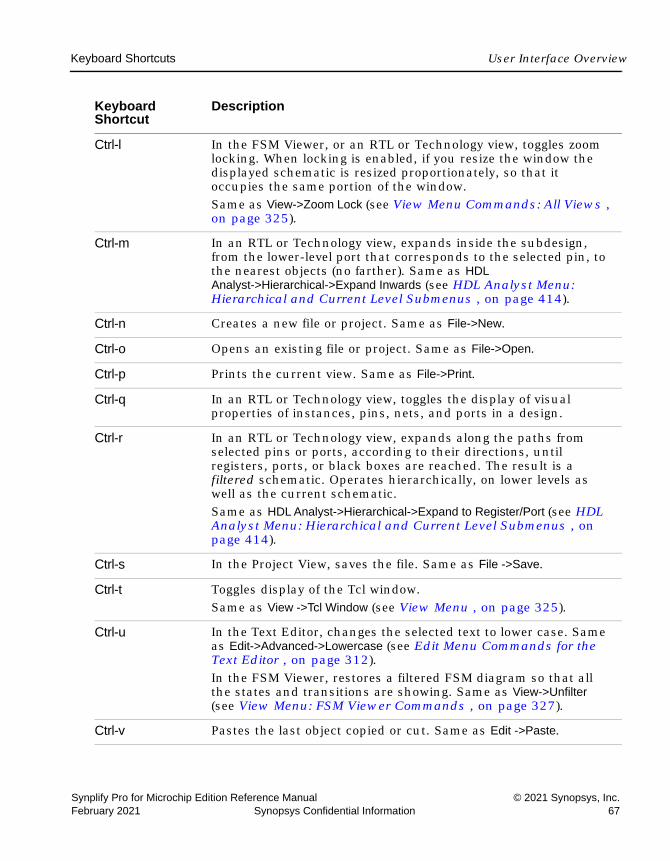
Keyboard Shortcuts User Interface Overview
Synplify Pro for Microchip Edition Reference Manual © 2021 Synopsys, Inc.February 2021 Synopsys Confidential Information 67
Ctrl-l In the FSM Viewer, or an RTL or Technology view, toggles zoom locking. When locking is enabled, if you resize the window the displayed schematic is resized proportionately, so that it occupies the same portion of the window.Same as View->Zoom Lock (see View Menu Commands: All Views , on page 325).
Ctrl-m In an RTL or Technology view, expands inside the subdesign, from the lower-level port that corresponds to the selected pin, to the nearest objects (no farther). Same as HDL Analyst->Hierarchical->Expand Inwards (see HDL Analyst Menu: Hierarchical and Current Level Submenus , on page 414).
Ctrl-n Creates a new file or project. Same as File->New.
Ctrl-o Opens an existing file or project. Same as File->Open.
Ctrl-p Prints the current view. Same as File->Print.
Ctrl-q In an RTL or Technology view, toggles the display of visual properties of instances, pins, nets, and ports in a design.
Ctrl-r In an RTL or Technology view, expands along the paths from selected pins or ports, according to their directions, until registers, ports, or black boxes are reached. The result is a filtered schematic. Operates hierarchically, on lower levels as well as the current schematic. Same as HDL Analyst->Hierarchical->Expand to Register/Port (see HDL Analyst Menu: Hierarchical and Current Level Submenus , on page 414).
Ctrl-s In the Project View, saves the file. Same as File ->Save.
Ctrl-t Toggles display of the Tcl window.Same as View ->Tcl Window (see View Menu , on page 325).
Ctrl-u In the Text Editor, changes the selected text to lower case. Same as Edit->Advanced->Lowercase (see Edit Menu Commands for the Text Editor , on page 312).In the FSM Viewer, restores a filtered FSM diagram so that all the states and transitions are showing. Same as View->Unfilter (see View Menu: FSM Viewer Commands , on page 327).
Ctrl-v Pastes the last object copied or cut. Same as Edit ->Paste.
Keyboard Shortcut
Description
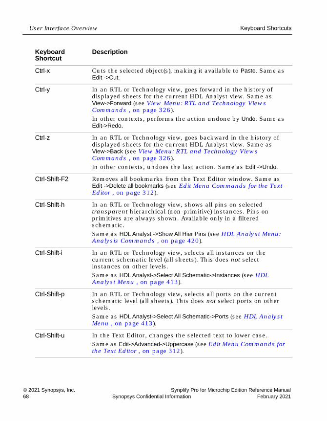
LO
User Interface Overview Keyboard Shortcuts
© 2021 Synopsys, Inc. Synplify Pro for Microchip Edition Reference Manual68 Synopsys Confidential Information February 2021
Ctrl-x Cuts the selected object(s), making it available to Paste. Same as Edit ->Cut.
Ctrl-y In an RTL or Technology view, goes forward in the history of displayed sheets for the current HDL Analyst view. Same as View->Forward (see View Menu: RTL and Technology Views Commands , on page 326).In other contexts, performs the action undone by Undo. Same as Edit->Redo.
Ctrl-z In an RTL or Technology view, goes backward in the history of displayed sheets for the current HDL Analyst view. Same as View->Back (see View Menu: RTL and Technology Views Commands , on page 326).In other contexts, undoes the last action. Same as Edit ->Undo.
Ctrl-Shift-F2 Removes all bookmarks from the Text Editor window. Same as Edit ->Delete all bookmarks (see Edit Menu Commands for the Text Editor , on page 312).
Ctrl-Shift-h In an RTL or Technology view, shows all pins on selected transparent hierarchical (non-primitive) instances. Pins on primitives are always shown. Available only in a filtered schematic. Same as HDL Analyst ->Show All Hier Pins (see HDL Analyst Menu: Analysis Commands , on page 420).
Ctrl-Shift-i In an RTL or Technology view, selects all instances on the current schematic level (all sheets). This does not select instances on other levels. Same as HDL Analyst->Select All Schematic->Instances (see HDL Analyst Menu , on page 413).
Ctrl-Shift-p In an RTL or Technology view, selects all ports on the current schematic level (all sheets). This does not select ports on other levels. Same as HDL Analyst->Select All Schematic->Ports (see HDL Analyst Menu , on page 413).
Ctrl-Shift-u In the Text Editor, changes the selected text to lower case. Same as Edit->Advanced->Uppercase (see Edit Menu Commands for the Text Editor , on page 312).
Keyboard Shortcut
Description
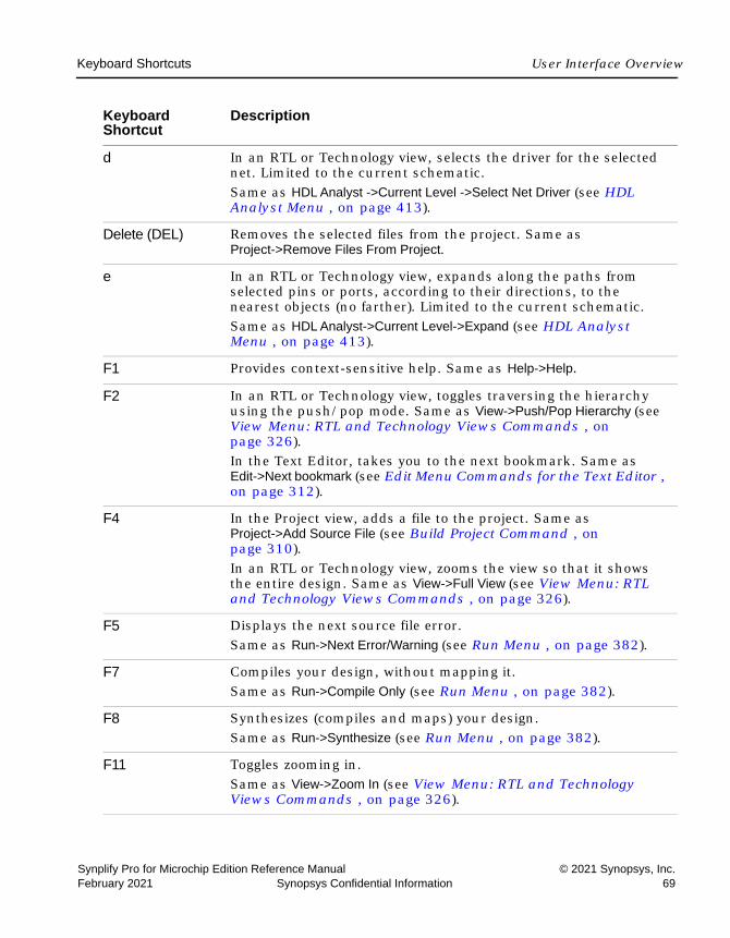
Keyboard Shortcuts User Interface Overview
Synplify Pro for Microchip Edition Reference Manual © 2021 Synopsys, Inc.February 2021 Synopsys Confidential Information 69
d In an RTL or Technology view, selects the driver for the selected net. Limited to the current schematic. Same as HDL Analyst ->Current Level ->Select Net Driver (see HDL Analyst Menu , on page 413).
Delete (DEL) Removes the selected files from the project. Same as Project->Remove Files From Project.
e In an RTL or Technology view, expands along the paths from selected pins or ports, according to their directions, to the nearest objects (no farther). Limited to the current schematic. Same as HDL Analyst->Current Level->Expand (see HDL Analyst Menu , on page 413).
F1 Provides context-sensitive help. Same as Help->Help.
F2 In an RTL or Technology view, toggles traversing the hierarchy using the push/pop mode. Same as View->Push/Pop Hierarchy (see View Menu: RTL and Technology Views Commands , on page 326).In the Text Editor, takes you to the next bookmark. Same as Edit->Next bookmark (see Edit Menu Commands for the Text Editor , on page 312).
F4 In the Project view, adds a file to the project. Same as Project->Add Source File (see Build Project Command , on page 310). In an RTL or Technology view, zooms the view so that it shows the entire design. Same as View->Full View (see View Menu: RTL and Technology Views Commands , on page 326).
F5 Displays the next source file error. Same as Run->Next Error/Warning (see Run Menu , on page 382).
F7 Compiles your design, without mapping it. Same as Run->Compile Only (see Run Menu , on page 382).
F8 Synthesizes (compiles and maps) your design. Same as Run->Synthesize (see Run Menu , on page 382).
F11 Toggles zooming in. Same as View->Zoom In (see View Menu: RTL and Technology Views Commands , on page 326).
Keyboard Shortcut
Description

LO
User Interface Overview Keyboard Shortcuts
© 2021 Synopsys, Inc. Synplify Pro for Microchip Edition Reference Manual70 Synopsys Confidential Information February 2021
F12 In an RTL or Technology view, filters your entire design to show only the selected objects. Same as HDL Analyst->Filter Schematic - see HDL Analyst Menu: Filtering and Flattening Commands , on page 416.
i In an RTL or Technology view, selects instances connected to the selected net. Limited to the current schematic. Same as HDL Analyst->Current Level->Select Net Instances (see HDL Analyst Menu , on page 413).
j In an RTL or Technology view, displays the unfiltered schematic sheet that contains the net driver for the selected net. Same as HDL Analyst->Current Level->Goto Net Driver (see HDL Analyst Menu , on page 413).
r In an RTL or Technology view, expands along the paths from selected pins or ports, according to their directions, until registers, ports, or black boxes are reached. The result is a filtered schematic. Limited to the current schematic. Same as HDL Analyst ->Current Level->Expand to Register/Port (see HDL Analyst Menu , on page 413).
Shift-F2 In the Text Editor, takes you to the previous bookmark.
Shift-F4 Allows you to add source files to your project (Project->Add Source Files).
Shift-F5 Displays the previous source file error. Same as Run->Previous Error/Warning (see Run Menu , on page 382).
Shift-F7 Checks source file syntax. Same as Run->Syntax Check (see Run Menu , on page 382).
Shift-F8 Checks synthesis. Same as Run->Synthesis Check (see Run Menu , on page 382).
Shift-F10 Checks the timing constraints in the constraint files in your project and generates a report (project_name_cck.rpt).Same as Run->Constraint Check (see Run Menu , on page 382).In an RTL or Technology view, lets you pan (scroll) the schematic by dragging it with the mouse. Same as View ->Pan (see View Menu: RTL and Technology Views Commands , on page 326).
Keyboard Shortcut
Description

Keyboard Shortcuts User Interface Overview
Synplify Pro for Microchip Edition Reference Manual © 2021 Synopsys, Inc.February 2021 Synopsys Confidential Information 71
Shift-F11 Toggles zooming out.Same as View->Zoom Out (see View Menu , on page 325).
Shift-Left Arrow Displays the previous sheet of a multiple-sheet schematic.
Shift-Right Arrow Displays the next sheet of a multiple-sheet schematic.
Shift-s Dissolves the selected instances, showing their lower-level details. Dissolving an instance one level replaces it, in the current sheet, by what you would see if you pushed into it using the push/pop mode. The rest of the sheet (not selected) remains unchanged. The number of levels dissolved is the Dissolve Levels value in the Schematic Options dialog box. The type (filtered or unfiltered) of the resulting schematic is unchanged from that of the current schematic. However, the effect of the command is different in filtered and unfiltered schematics.Same as HDL Analyst ->Dissolve Instances - see Dissolve Instances , on page 422.
Keyboard Shortcut
Description

LO
User Interface Overview Buttons and Options
© 2021 Synopsys, Inc. Synplify Pro for Microchip Edition Reference Manual72 Synopsys Confidential Information February 2021
Buttons and OptionsThe Project view contains several buttons and a few additional features that give you immediate access to some of the more common commands and user options.
The following table describes the Project View buttons and options.
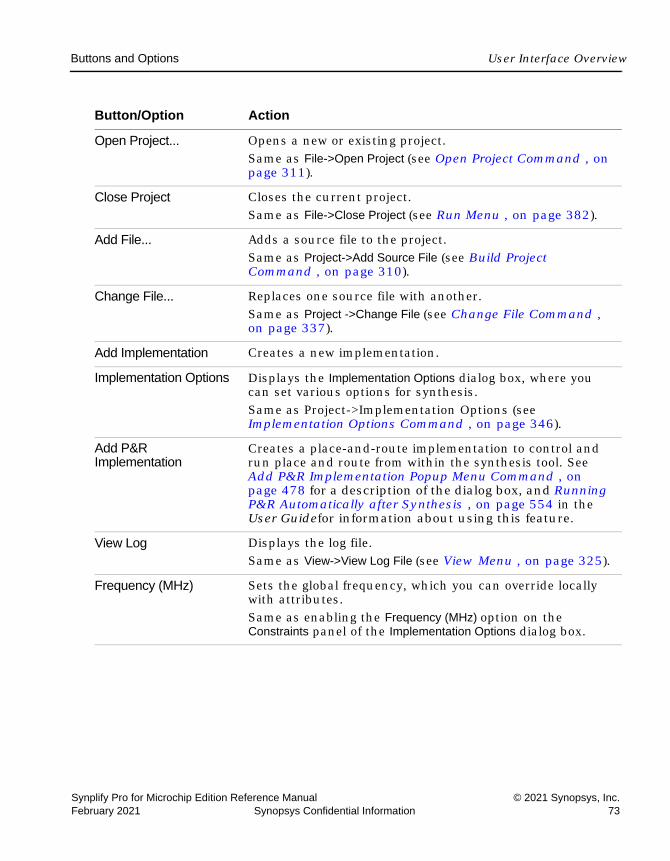
Buttons and Options User Interface Overview
Synplify Pro for Microchip Edition Reference Manual © 2021 Synopsys, Inc.February 2021 Synopsys Confidential Information 73
Button/Option Action
Open Project... Opens a new or existing project.Same as File->Open Project (see Open Project Command , on page 311).
Close Project Closes the current project.Same as File->Close Project (see Run Menu , on page 382).
Add File... Adds a source file to the project. Same as Project->Add Source File (see Build Project Command , on page 310).
Change File... Replaces one source file with another. Same as Project ->Change File (see Change File Command , on page 337).
Add Implementation Creates a new implementation.
Implementation Options Displays the Implementation Options dialog box, where you can set various options for synthesis.Same as Project->Implementation Options (see Implementation Options Command , on page 346).
Add P&R Implementation
Creates a place-and-route implementation to control and run place and route from within the synthesis tool. See Add P&R Implementation Popup Menu Command , on page 478 for a description of the dialog box, and Running P&R Automatically after Synthesis , on page 554 in the User Guidefor information about using this feature.
View Log Displays the log file. Same as View->View Log File (see View Menu , on page 325).
Frequency (MHz) Sets the global frequency, which you can override locally with attributes. Same as enabling the Frequency (MHz) option on the Constraints panel of the Implementation Options dialog box.

LO
User Interface Overview Buttons and Options
© 2021 Synopsys, Inc. Synplify Pro for Microchip Edition Reference Manual74 Synopsys Confidential Information February 2021
Auto Constrain When Auto Constrain is enabled and no clocks are defined, the software automatically constrains the design to achieve best possible timing by reducing periods of individual clock and the timing of any timed I/O paths in successive steps.See Using Auto Constraints , on page 376 in the User Guide for detailed information about using this option. You can also set this option on the Constraints panel of the Implementation Options dialog box.
FSM Compiler Turning on this option enables special FSM optimizations. Same as enabling the FSM Compiler option on the Options panel of the Implementation Options dialog box (see Optimizing State Machines , on page 424 in the User Guide).
FSM Explorer When enabled, the FSM Explorer selects an encoding style for the finite state machines in your design.Same as enabling the FSM Explorer option on the Options panel of the Implementation Options dialog box. For more information, see Running the FSM Compiler , on page 425 in the User Guide.
Button/Option Action
Buttons and Options User Interface Overview
Synplify Pro for Microchip Edition Reference Manual © 2021 Synopsys, Inc.February 2021 Synopsys Confidential Information 75
Resource Sharing When enabled, makes the compiler use resource sharing techniques. This option does not affect resource sharing by the mapper. The option is the same as the Resource Sharing option on the Options panel of the Implementation Options dialog box. See Sharing Resources , on page 422 in the User Guide for usage details.
Retiming When enabled, improves the timing performance of sequential circuits. The retiming process moves storage devices (flip-flops) across computational elements with no memory (gates/LUTs) to improve the performance of the circuit. This option also adds a retiming report to the log file.Same as enabling the Retiming option on the Options panel of the Implementation Options dialog box. Use the syn_allow_retiming attribute to enable or disable retiming for individual flip-flops. See syn_allow_retiming , on page 59 for syntax details.
Run Runs synthesis (compilation and mapping). Same as the Run->Run command (see Run Menu , on page 382).
Button/Option Action

LO
User Interface Overview Buttons and Options
© 2021 Synopsys, Inc. Synplify Pro for Microchip Edition Reference Manual76 Synopsys Confidential Information February 2021
Synplify Pro for Microchip Edition Reference Manual © 2021 Synopsys, Inc.February 2021 Synopsys Confidential Information 77
C H A P T E R 3
HDL Analyst Tool
The HDL Analyst tool helps you examine your design and synthesis results, and analyze how you can improve design performance and area.
The following describe the HDL Analyst tool and the operations you can perform with it.
• HDL Analyst Views and Commands, on page 78
• Schematic Objects and Their Display, on page 88
• Basic Operations on Schematic Objects, on page 97
• Multiple-sheet Schematics, on page 102
• Exploring Design Hierarchy, on page 105
• Filtering and Flattening Schematics, on page 113
• Timing Information and Critical Paths, on page 119

LO
HDL Analyst Tool HDL Analyst Views and Commands
© 2021 Synopsys, Inc. Synplify Pro for Microchip Edition Reference Manual78 Synopsys Confidential Information February 2021
HDL Analyst Views and CommandsThe HDL Analyst tool graphically displays information in two schematic views: the RTL and Technology views (see RTL View, on page 78 and Technology View, on page 80 for information). The graphic representation is useful for analyzing and debugging your design, because you can visualize where coding changes or timing constraints might reduce area or increase performance.
This section gives you information about the following:
• Hierarchy Browser, on page 82
• FSM Viewer Window, on page 83
• Filtered and Unfiltered Schematic Views, on page 85
• Accessing HDL Analyst Commands, on page 86
RTL ViewThe RTL view provides a high-level, technology-independent, graphic repre-sentation of your design after compilation, using technology-independent components like variable-width adders, registers, large multiplexers, and state machines. RTL views correspond to the srs netlist files generated during compilation. RTL views are only available after your design has been success-fully compiled. For information about the other HDL Analyst view (the Technology view generated after mapping), see Technology View, on page 80.
To display an RTL view, first compile or synthesize your design, then select HDL Analyst->RTL and choose Hierarchical View or Flattened View, or click the RTL icon ( ).
An RTL view has two panes: a Hierarchy Browser on the left and an RTL schematic on the right. You can drag the pane divider with the mouse to change the relative pane sizes. For more information about the Hierarchy Browser, see Hierarchy Browser, on page 82. Your design is drawn as a set of schematics. The schematic for a design module (or the top level) consists of one or more sheets, only one of which is visible in a given view at any time. The title bar of the window indicates the current hierarchical schematic level, the current sheet, and the total number of sheets for that level.
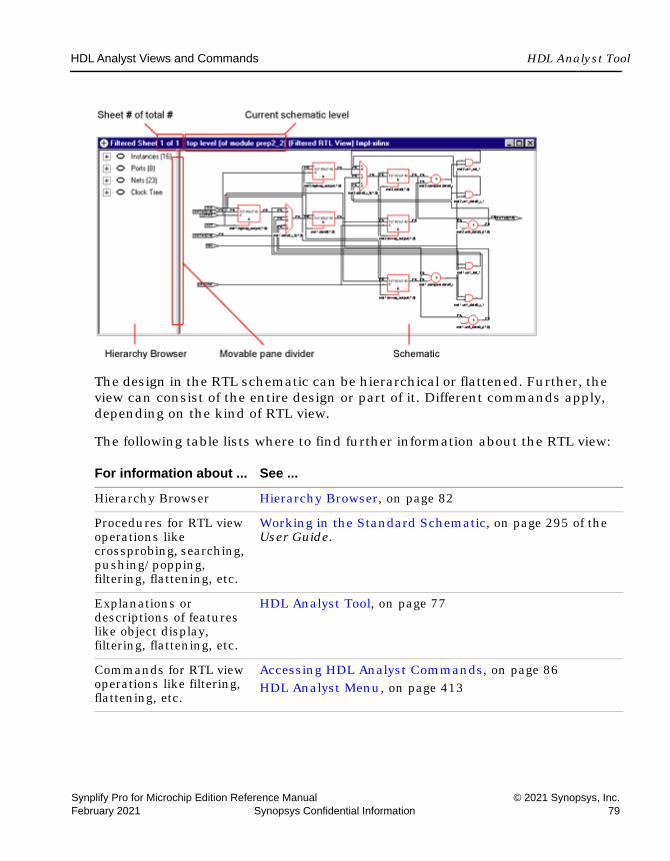
HDL Analyst Views and Commands HDL Analyst Tool
Synplify Pro for Microchip Edition Reference Manual © 2021 Synopsys, Inc.February 2021 Synopsys Confidential Information 79
The design in the RTL schematic can be hierarchical or flattened. Further, the view can consist of the entire design or part of it. Different commands apply, depending on the kind of RTL view.
The following table lists where to find further information about the RTL view:
For information about ... See ...
Hierarchy Browser Hierarchy Browser, on page 82
Procedures for RTL view operations like crossprobing, searching, pushing/popping, filtering, flattening, etc.
Working in the Standard Schematic, on page 295 of the User Guide.
Explanations or descriptions of features like object display, filtering, flattening, etc.
HDL Analyst Tool, on page 77
Commands for RTL view operations like filtering, flattening, etc.
Accessing HDL Analyst Commands, on page 86HDL Analyst Menu, on page 413

LO
HDL Analyst Tool HDL Analyst Views and Commands
© 2021 Synopsys, Inc. Synplify Pro for Microchip Edition Reference Manual80 Synopsys Confidential Information February 2021
Technology ViewA Technology view provides a low-level, technology-specific view of your design after mapping, using components such as look-up tables, cascade and carry chains, multiplexers, and flip-flops. Technology views are only available after your design has been synthesized (compiled and mapped). For informa-tion about the other HDL Analyst view (the RTL view generated after compila-tion), see RTL View, on page 78.
To display a Technology view, first synthesize your design, and then either select a view from the HDL Analyst->Technology menu (Hierarchical View, Flattened View, Flattened to Gates View, Hierarchical Critical Path, or Flattened Critical Path) or select the Technology view icon ( ).
A Technology view has two panes: a Hierarchy Browser on the left and an RTL schematic on the right. You can drag the pane divider with the mouse to change the relative pane sizes. For more information about the Hierarchy Browser, see Hierarchy Browser, on page 82. Your design is drawn as a set of schematics at different design levels. The schematic for a design module (or the top level) consists of one or more sheets, only one of which is visible in a given view at any time. The title bar of the window indicates the current schematic level, the current sheet, and the total number of sheets for that level.
Viewing commands like zooming, panning, etc.
View Menu: RTL and Technology Views Commands, on page 326
History commands: Back and Forward
View Menu: RTL and Technology Views Commands, on page 326
Search command Find Command (HDL Analyst), on page 317
For information about ... See ...

HDL Analyst Views and Commands HDL Analyst Tool
Synplify Pro for Microchip Edition Reference Manual © 2021 Synopsys, Inc.February 2021 Synopsys Confidential Information 81
The schematic design can be hierarchical or flattened. Further, the view can consist of the entire design or a part of it. Different commands apply, depending on the kind of view. In addition to all the features available in RTL views, Technology views have two additional features: critical path filtering and flattening to gates.
The following table lists where to find further information about the Technology view:
For information about ... See ...
Hierarchy Browser Hierarchy Browser, on page 82
Procedures for Technology view operations like crossprobing, searching, pushing/popping, filtering, flattening, etc.
Working in the Standard Schematic, on page 295 of the User Guide
Explanations or descriptions of features like object display, filtering, flattening, etc.
HDL Analyst Tool, on page 77
Commands for Technology view operations like filtering, flattening, etc.
Accessing HDL Analyst Commands, on page 86HDL Analyst Menu, on page 413
LO
HDL Analyst Tool HDL Analyst Views and Commands
© 2021 Synopsys, Inc. Synplify Pro for Microchip Edition Reference Manual82 Synopsys Confidential Information February 2021
Hierarchy BrowserThe Hierarchy Browser is the left pane in the RTL and Technology views. (See RTL View, on page 78 and Technology View, on page 80.) The Hierarchy Browser categorizes the design objects in a series of trees, and lets you browse the design hierarchy or select objects. Selecting an object in the Browser selects that object in the schematic. The objects are organized as shown in the following table, with a symbol that indicates the object type. See Hierarchy Browser Symbols, on page 83 for common symbols.
A tree node can be expanded or collapsed by clicking the associated icons: the square plus ( ) or minus ( ) icons, respectively. You can also expand or collapse all trees at the same time by right-clicking in the Hierarchy Browser and choosing Expand All or Collapse All.
You can use the keyboard arrow keys (left, right, up, down) to move between objects in the Hierarchy Browser, or you can use the scroll bar. Use the Shift or Ctrl keys to select multiple objects. See Navigating With a Hierarchy Browser, on page 109 for more information about using the Hierarchy Browser for navigation and crossprobing.
Viewing commands like zooming, panning, etc.
View Menu: RTL and Technology Views Commands, on page 326
History commands: Back and Forward
View Menu: RTL and Technology Views Commands, on page 326
Search command Find Command (HDL Analyst), on page 317
Instances Lists all the instances and primitives in the design. In a Technology view, it includes all technology-specific primitives.
Ports Lists all the ports in the design.
Nets Lists all the nets in the design.
Clock Tree Lists all the instances and ports that drive clock pins in an RTL view. If you select everything listed under Clock Tree and then use the Filter Schematic command, you see a filtered view of all clock pin drivers in your design. Registers are not shown in the resulting schematic, unless they drive clocks. This view can help you determine what to define as clocks.
For information about ... See ...

HDL Analyst Views and Commands HDL Analyst Tool
Synplify Pro for Microchip Edition Reference Manual © 2021 Synopsys, Inc.February 2021 Synopsys Confidential Information 83
Hierarchy Browser SymbolsCommon symbols used in Hierarchy Browsers are listed in the following table.
FSM Viewer WindowPushing down into a state machine primitive in the RTL view displays the FSM Viewer and enables the FSM toolbar. The FSM Viewer contains graphical information about the finite state machines (FSMs) in your design. The window has a state-transition diagram and tables of transitions and state encodings.
Symbol Description Symbol Description
Folder Buffer
Input port AND gate
Output port NAND gate
Bidirectional port OR gate
Net NOR gate
Other primitive instance XOR gate
Hierarchical instance XNOR gate
Technology-specific primitive or inferred ROM
Adder
Registeror inferred state machine
Multiplier
Multiplexer Equal comparator
Tristate Less-than comparator
Inverter Less-than-or-equal comparator
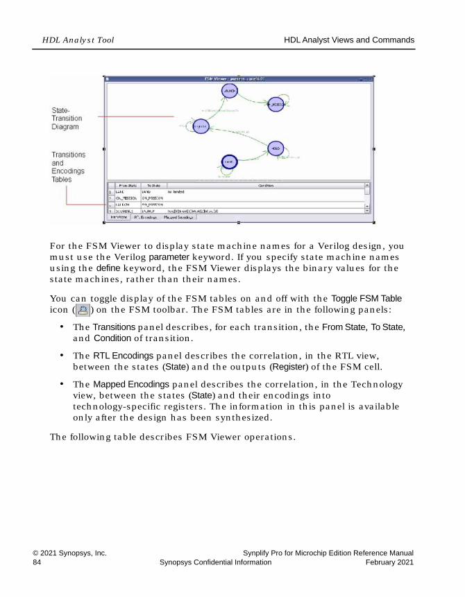
LO
HDL Analyst Tool HDL Analyst Views and Commands
© 2021 Synopsys, Inc. Synplify Pro for Microchip Edition Reference Manual84 Synopsys Confidential Information February 2021
For the FSM Viewer to display state machine names for a Verilog design, you must use the Verilog parameter keyword. If you specify state machine names using the define keyword, the FSM Viewer displays the binary values for the state machines, rather than their names.
You can toggle display of the FSM tables on and off with the Toggle FSM Table icon ( ) on the FSM toolbar. The FSM tables are in the following panels:
• The Transitions panel describes, for each transition, the From State, To State, and Condition of transition.
• The RTL Encodings panel describes the correlation, in the RTL view, between the states (State) and the outputs (Register) of the FSM cell.
• The Mapped Encodings panel describes the correlation, in the Technology view, between the states (State) and their encodings into technology-specific registers. The information in this panel is available only after the design has been synthesized.
The following table describes FSM Viewer operations.
HDL Analyst Views and Commands HDL Analyst Tool
Synplify Pro for Microchip Edition Reference Manual © 2021 Synopsys, Inc.February 2021 Synopsys Confidential Information 85
Filtered and Unfiltered Schematic ViewsHDL Analyst views (RTL View, on page 78 and Technology View, on page 80) consist of schematics that let you analyze your design graphically. The schematics can be filtered or unfiltered. The distinction is important because the kind of view determines how objects are displayed for certain commands.
• Unfiltered schematics display all the objects in your design, at appro-priate hierarchical levels.
• Filtered schematics show only a subset of the objects in your design, because the other objects have been filtered out by some operation. The Hierarchy Browser in the filtered view always list all the objects in the design, not just the filtered objects. Some commands, such as HDL Analyst -> Show Context, are only available in filtered schematics. Views with a filtered schematic have the word Filtered in the title bar.
To accomplish this ... Do this ...
Open the FSM Viewer Run the FSM Compiler or the FSM Explorer. Use the push/pop mode in the RTL view to push down into the FSM and open the FSM Viewer window.
Hide/display the table Use the FSM icons.
Filter selected states and their transitions
Select the states. Right-click and choose the filter criteria from the popup, or use the FSM icons.
Display the encoding properties of a state
Select a state. Right-click to display its encoding properties (RTL or Mapped).
Display properties for the state machine
Right-click the window, outside the state-transition diagram. The property sheet shows the selected encoding method, the number of states, and the total number of transitions among states.
Crossprobe Double-click a register in an RTL or Technology view to see the corresponding code. Select a state in the FSM view to highlight the corresponding code or register in other open views.

LO
HDL Analyst Tool HDL Analyst Views and Commands
© 2021 Synopsys, Inc. Synplify Pro for Microchip Edition Reference Manual86 Synopsys Confidential Information February 2021
Filtering commands affect only the displayed schematic, not the under-lying design. See the following topics:
• For a detailed description of filtering, see Filtering and Flattening Schematics, on page 113.
• For procedures on using filtering, see Filtering Schematics, on page 340 in the User Guide.
Accessing HDL Analyst CommandsYou can access HDL Analyst commands in many ways, depending on the active view, the currently selected objects, and other design context factors. The software offers these alternatives to access the commands:
• HDL Analyst and View menus
• HDL Analyst popup menus appear when you right-click in an HDL Analyst view. The popup menu is context-sensitive, and includes commonly used commands from the HDL Analyst and View menus, as well as some additional commands.
• HDL Analyst toolbar icons provide shortcuts to commonly used commands
For brevity, this document primarily refers to the menu method of accessing the commands and does not list alternative access methods.
See also:
• HDL Analyst Menu, on page 413
• View Menu, on page 325
• RTL and Technology Views Popup Menus, on page 483

HDL Analyst Views and Commands HDL Analyst Tool
Synplify Pro for Microchip Edition Reference Manual © 2021 Synopsys, Inc.February 2021 Synopsys Confidential Information 87
• Analyst Toolbar, on page 59
LO
HDL Analyst Tool Schematic Objects and Their Display
© 2021 Synopsys, Inc. Synplify Pro for Microchip Edition Reference Manual88 Synopsys Confidential Information February 2021
Schematic Objects and Their DisplaySchematic objects are the objects that you manipulate in an HDL Analyst schematic: instances, ports, and nets. Instances can be categorized in different ways, depending on the operation: hidden/unhidden, trans-parent/opaque, or primitive/hierarchical. The following topics describe schematic objects and the display of associated information in more detail:
• Object Information, on page 88
• Sheet Connectors, on page 89
• Primitive and Hierarchical Instances, on page 90
• Hidden Hierarchical Instances, on page 93
• Transparent and Opaque Display of Hierarchical Instances, on page 91
• Schematic Display, on page 93
For most objects, you select them to perform an operation. For some objects like sheet connectors, you do not select them but right-click on them and select from the popup menu commands.
Object InformationTo obtain information about specific objects, you can view object properties with the Properties command from the right-click popup menu, or place the pointer over the object and view the object information displayed. With the latter method, information about the object displays in these two places until you move the pointer away:
• The status bar at the bottom of the synthesis window displays the name of the instance, net, port, or sheet connector and other relevant informa-tion. If HDL Analyst->Show Timing Information is enabled, the status bar also displays timing information for the object. Here is an example of the status bar information for a net:
Net clock (local net clock) Fanout=4You can enable and disable the display of status bar information by toggling the command View -> Status Bar.
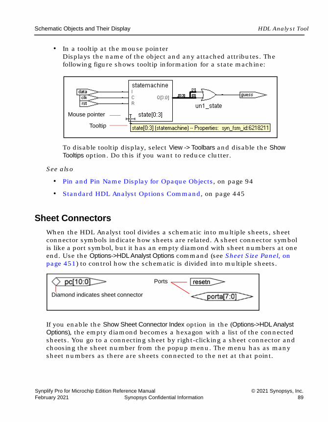
Schematic Objects and Their Display HDL Analyst Tool
Synplify Pro for Microchip Edition Reference Manual © 2021 Synopsys, Inc.February 2021 Synopsys Confidential Information 89
• In a tooltip at the mouse pointerDisplays the name of the object and any attached attributes. The following figure shows tooltip information for a state machine:
To disable tooltip display, select View -> Toolbars and disable the Show Tooltips option. Do this if you want to reduce clutter.
See also
• Pin and Pin Name Display for Opaque Objects, on page 94
• Standard HDL Analyst Options Command, on page 445
Sheet ConnectorsWhen the HDL Analyst tool divides a schematic into multiple sheets, sheet connector symbols indicate how sheets are related. A sheet connector symbol is like a port symbol, but it has an empty diamond with sheet numbers at one end. Use the Options->HDL Analyst Options command (see Sheet Size Panel, on page 451) to control how the schematic is divided into multiple sheets.
If you enable the Show Sheet Connector Index option in the (Options->HDL Analyst Options), the empty diamond becomes a hexagon with a list of the connected sheets. You go to a connecting sheet by right-clicking a sheet connector and choosing the sheet number from the popup menu. The menu has as many sheet numbers as there are sheets connected to the net at that point.
Tooltip
Mouse pointer
Diamond indicates sheet connector
Ports
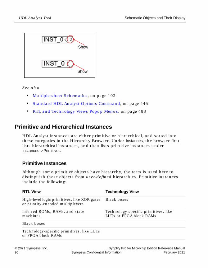
LO
HDL Analyst Tool Schematic Objects and Their Display
© 2021 Synopsys, Inc. Synplify Pro for Microchip Edition Reference Manual90 Synopsys Confidential Information February 2021
See also
• Multiple-sheet Schematics, on page 102
• Standard HDL Analyst Options Command, on page 445
• RTL and Technology Views Popup Menus, on page 483
Primitive and Hierarchical InstancesHDL Analyst instances are either primitive or hierarchical, and sorted into these categories in the Hierarchy Browser. Under Instances, the browser first lists hierarchical instances, and then lists primitive instances under Instances->Primitives.
Primitive InstancesAlthough some primitive objects have hierarchy, the term is used here to distinguish these objects from user-defined hierarchies. Primitive instances include the following:
RTL View Technology View
High-level logic primitives, like XOR gates or priority-encoded multiplexers
Black boxes
Inferred ROMs, RAMs, and state machines
Technology-specific primitives, like LUTs or FPGA block RAMs
Black boxes
Technology-specific primitives, like LUTs or FPGA block RAMs
Show
Show
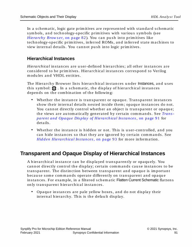
Schematic Objects and Their Display HDL Analyst Tool
Synplify Pro for Microchip Edition Reference Manual © 2021 Synopsys, Inc.February 2021 Synopsys Confidential Information 91
In a schematic, logic gate primitives are represented with standard schematic symbols, and technology-specific primitives with various symbols (see Hierarchy Browser, on page 82). You can push into primitives like technology-specific primitives, inferred ROMs, and inferred state machines to view internal details. You cannot push into logic primitives.
Hierarchical InstancesHierarchical instances are user-defined hierarchies; all other instances are considered to be primitives. Hierarchical instances correspond to Verilog modules and VHDL entities.
The Hierarchy Browser lists hierarchical instances under Instances, and uses this symbol: . In a schematic, the display of hierarchical instances depends on the combination of the following:
• Whether the instance is transparent or opaque. Transparent instances show their internal details nested inside them; opaque instances do not. You cannot directly control whether an object is transparent or opaque; the views are automatically generated by certain commands. See Trans-parent and Opaque Display of Hierarchical Instances, on page 91 for details.
• Whether the instance is hidden or not. This is user-controlled, and you can hide instances so that they are ignored by certain commands. See Hidden Hierarchical Instances, on page 93 for more information.
Transparent and Opaque Display of Hierarchical InstancesA hierarchical instance can be displayed transparently or opaquely. You cannot directly control the display; certain commands cause instances to be transparent. The distinction between transparent and opaque is important because some commands operate differently on transparent and opaque instances. For example, in a filtered schematic Flatten Current Schematic flattens only transparent hierarchical instances.
• Opaque instances are pale yellow boxes, and do not display their internal hierarchy. This is the default display.
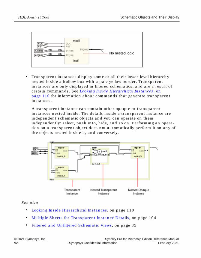
LO
HDL Analyst Tool Schematic Objects and Their Display
© 2021 Synopsys, Inc. Synplify Pro for Microchip Edition Reference Manual92 Synopsys Confidential Information February 2021
• Transparent instances display some or all their lower-level hierarchy nested inside a hollow box with a pale yellow border. Transparent instances are only displayed in filtered schematics, and are a result of certain commands. See Looking Inside Hierarchical Instances, on page 110 for information about commands that generate transparent instances.
A transparent instance can contain other opaque or transparent instances nested inside. The details inside a transparent instance are independent schematic objects and you can operate on them independently: select, push into, hide, and so on. Performing an opera-tion on a transparent object does not automatically perform it on any of the objects nested inside it, and conversely.
See also
• Looking Inside Hierarchical Instances, on page 110
• Multiple Sheets for Transparent Instance Details, on page 104
• Filtered and Unfiltered Schematic Views, on page 85
No nested logic
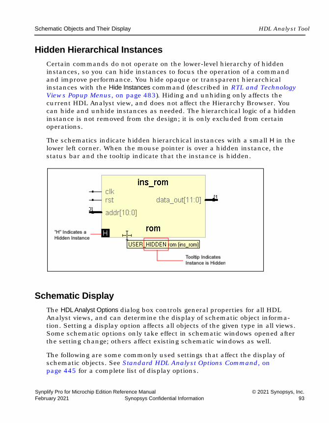
Schematic Objects and Their Display HDL Analyst Tool
Synplify Pro for Microchip Edition Reference Manual © 2021 Synopsys, Inc.February 2021 Synopsys Confidential Information 93
Hidden Hierarchical InstancesCertain commands do not operate on the lower-level hierarchy of hidden instances, so you can hide instances to focus the operation of a command and improve performance. You hide opaque or transparent hierarchical instances with the Hide Instances command (described in RTL and Technology Views Popup Menus, on page 483). Hiding and unhiding only affects the current HDL Analyst view, and does not affect the Hierarchy Browser. You can hide and unhide instances as needed. The hierarchical logic of a hidden instance is not removed from the design; it is only excluded from certain operations.
The schematics indicate hidden hierarchical instances with a small H in the lower left corner. When the mouse pointer is over a hidden instance, the status bar and the tooltip indicate that the instance is hidden.
Schematic DisplayThe HDL Analyst Options dialog box controls general properties for all HDL Analyst views, and can determine the display of schematic object informa-tion. Setting a display option affects all objects of the given type in all views. Some schematic options only take effect in schematic windows opened after the setting change; others affect existing schematic windows as well.
The following are some commonly used settings that affect the display of schematic objects. See Standard HDL Analyst Options Command, on page 445 for a complete list of display options.
LO
HDL Analyst Tool Schematic Objects and Their Display
© 2021 Synopsys, Inc. Synplify Pro for Microchip Edition Reference Manual94 Synopsys Confidential Information February 2021
Pin and Pin Name Display for Opaque ObjectsAlthough it always displays the pins, the software does not automatically display pin names for opaque hierarchical instances, technology-specific primitives, RAMS, ROMs, and state machines. To display pin names for these objects, enable Options-> HDL Analyst Options->Text->Show Pin Name. The following figures illustrate this display. The first figure shows pins and pin names of an opaque hierarchical instance, and the second figure shows the pins of a technology-specific primitive with its cell contents not displayed.
Option Controls the display of ...
Show Cell Interior Internal logic of technology-specific primitives
Compress Buses Buses as bundles
Dissolve Levels Hierarchical levels in a view flattened with HDL Analyst -> Dissolve Instances or Dissolve to Gates, by setting the number of levels to dissolve.
InstancesFiltered InstancesInstances added for expansion
Instances on a schematic by setting limits to the number of instances displayed
Instance NameShow Conn NameShow Symbol NameShow Port Name
Object labels
Show Pin NameHDL Analyst->Show All Hier Pins
Pin names. See Pin and Pin Name Display for Opaque Objects , on page 94 and Pin and Pin Name Display for Transparent Objects , on page 95 for details.

Schematic Objects and Their Display HDL Analyst Tool
Synplify Pro for Microchip Edition Reference Manual © 2021 Synopsys, Inc.February 2021 Synopsys Confidential Information 95
Pin and Pin Name Display for Transparent ObjectsThis section discusses pin name display for transparent hierarchical instances in filtered views and technology-specific primitives.
Transparent Hierarchical InstancesIn a filtered schematic, some of the pins on a transparent hierarchical instance might not be displayed because of filtering. To display all the pins, select the instance and select HDL Analyst -> Show All Hier Pins.
LO
HDL Analyst Tool Schematic Objects and Their Display
© 2021 Synopsys, Inc. Synplify Pro for Microchip Edition Reference Manual96 Synopsys Confidential Information February 2021
To display pin names for the instance, enable Options->HDL Analyst Options->Text ->Show Pin Name. The software temporarily displays the pin name when you move the cursor over a pin. To keep the pin name displayed even after you move the cursor away, select the pin. The name remains until you select something else.
PrimitivesTo display pin names for technology primitives in the Technology view, enable Options-> HDL Analyst Options->Text->Show Pin Name. The software displays the pin names until the option is disabled. If Show Pin Name is enabled when Options-> HDL Analyst Options->General->Show Cell Interior is also enabled, the primitive is treated like a transparent hierarchical instance, and primitive pin names are only displayed when the cursor moves over the pins. To keep a pin name displayed even after you move the cursor away, select the pin. The name remains until you select something else.
See also:
• Standard HDL Analyst Options Command, on page 445
• Controlling the Amount of Logic on a Sheet, on page 102
• Analyzing Timing in Schematic Views, on page 358 in the User Guide

Basic Operations on Schematic Objects HDL Analyst Tool
Synplify Pro for Microchip Edition Reference Manual © 2021 Synopsys, Inc.February 2021 Synopsys Confidential Information 97
Basic Operations on Schematic ObjectsBasic operations on schematic objects include the following:
• Finding Schematic Objects, on page 97
• Selecting and Unselecting Schematic Objects, on page 98
• Crossprobing Objects, on page 99
• Dragging and Dropping Objects, on page 101
For information about other operations on schematics and schematic objects, see the following:
• Filtering and Flattening Schematics, on page 113
• Timing Information and Critical Paths, on page 119
• Multiple-sheet Schematics, on page 102
• Exploring Design Hierarchy, on page 105
Finding Schematic ObjectsYou can use the following techniques to find objects in the schematic. For step-by-step procedures using these techniques, see Finding Objects (Standard), on page 316 in the User Guide.
• Zooming and panning
• HDL Analyst Hierarchy Browser
You can use the Hierarchy Browser to browse and find schematic objects. This can be a quick way to locate an object by name if you are familiar with the design hierarchy. See Browsing With the Hierarchy Browser, on page 316 in the User Guide for details.
• Edit -> Find command
The Edit -> Find command is described in Find Command (HDL Analyst), on page 317. It displays the Object Query dialog box, which lists schematic objects by type (Instances, Symbols, Nets, or Ports) and lets you use wildcards to find objects by name. You can also fine-tune your search by setting a range for the search.

LO
HDL Analyst Tool Basic Operations on Schematic Objects
© 2021 Synopsys, Inc. Synplify Pro for Microchip Edition Reference Manual98 Synopsys Confidential Information February 2021
This command selects all found objects, whether or not they are displayed in the current schematic. Although you can search for hidden instances, you cannot find objects that are inside hidden instances at a lower level. Temporarily hiding an instance thus further refines the search range by excluding the internals of a a given instance. This can be very useful when working with transparent instances, because the lower-level details appear at the current level, and cannot be excluded by choosing Current Level Only. See Using Find for Hierarchical and Restricted Searches, on page 318 in the User Guide.
• Edit -> Find command combined with filtering
Edit->Find enhances filtering. Use Find to select by name and hierarchical level, and then filter the design to limit the display to the current selec-tion. Unselected objects are removed. Because Find only adds to the current selection (it never deselects anything already selected), you can use successive searches to build up exactly the selection you need, before filtering.
• Filtering before searching with Edit->Find
Filtering helps you to fine-tune the range of a search. You can search for objects just within a filtered schematic by limiting the search range to the Current Level Only.
Filtering adds to the expressive power of displaying search results. You can find objects on different sheets and filter them to see them all together at once. Filtering collapses the hierarchy visually, showing lower-level details nested inside transparent higher-level instances. The resulting display combines the advantage of a high-level, abstract view with detail-rich information from lower levels.
See Filtering and Flattening Schematics, on page 113 for further informa-tion.
Selecting and Unselecting Schematic ObjectsWhenever an object is selected in one place it is selected and highlighted everywhere else in the synthesis tool, including all Hierarchy Browsers, all schematics, and the Text Editor. Many commands operate on the currently selected objects, whether or not those objects are visible.
Basic Operations on Schematic Objects HDL Analyst Tool
Synplify Pro for Microchip Edition Reference Manual © 2021 Synopsys, Inc.February 2021 Synopsys Confidential Information 99
The following briefly list selection methods; for a concise table of selection procedures, see Selecting Objects in the RTL/Technology Views, on page 302 in the User Guide.
Using the Mouse to Select a Range of Schematic ObjectsIn a Hierarchy Browser, you can select a range of schematic objects by clicking the name of an object at one end of the range, then holding the Shift key while clicking the name of an object at the other end of the range.To use the mouse for selecting and unselecting objects in a schematic, the cross-hairs symbol ( ) must appear as the mouse pointer. If this is not currently the case, right-click the schematic background.
Using Commands to Select Schematic ObjectsYou can select and deselect schematic objects using the commands in the HDL Analyst menu, or use Edit->Find to find and select objects by name.
The HDL Analyst menu commands that affect selection include the following:
• Expansion commands like Expand, Expand to Register/Port, Expand Paths, and Expand Inwards select the objects that result from the expansion. This means that (except for Expand to Register/Port) you can perform successive expansions and expand the set of objects selected.
• The Select All Schematic and Select All Sheet commands select all instances or ports on the current schematic or sheet, respectively.
• The Select Net Driver and Select Net Instances commands select the appro-priate objects according to the hierarchical level you have chosen.
• Deselect All deselects all objects in all HDL Analyst views.
See also
• Finding Schematic Objects, on page 97
• HDL Analyst Menu, on page 413
Crossprobing ObjectsCrossprobing helps you diagnose where coding changes or timing constraints might reduce area or increase performance. When you crossprobe, you select an object in one place and it or its equivalent is automatically selected and
LO
HDL Analyst Tool Basic Operations on Schematic Objects
© 2021 Synopsys, Inc. Synplify Pro for Microchip Edition Reference Manual100 Synopsys Confidential Information February 2021
highlighted in other places. For example, selecting text in the Text Editor automatically selects the corresponding logic in all HDL Analyst views. Whenever a net is selected, it is highlighted through all the hierarchical instances it traverses, at all schematic levels.
Crossprobing Between Different ViewsYou can crossprobe objects (including logic inside hidden instances) between RTL views, Technology views, the FSM Viewer, HDL source code files, and other text files. Some RTL and source code objects are optimized away during synthesis, so they cannot be crossprobed to certain views.
The following table summarizes crossprobing to and from HDL Analyst (RTL and Technology) views. For information about crossprobing procedures, see Crossprobing (Standard), on page 329 in the User Guide.
From ... To ... Do this ...
Text Editor: log file
Text Editor: HDL source file
Double-click a log file note, error, or warning. The corresponding HDL source code appears in the Text Editor.
Text Editor: HDL code
Analyst view
FSM Viewer
The RTL view or Technology view must be open. Select the code in the Text Editor that corresponds to the object(s) you want to crossprobe. The object corresponding to the selected code is automatically selected in the target view, if an HDL source file is in the Text Editor. Otherwise, right-click and choose the Select in Analyst command. To cross-probe from text other than source code, first select Options->HDL Analyst Options and then enable Enhanced Text Crossprobing.
FSM Viewer Analyst view The target view must be open. The state machine must be encoded with the onehot style to crossprobe from the transition table. Select a state anywhere in the FSM Viewer (bubble diagram or transition table). The corresponding object is automatically selected in the HDL Analyst view.

Basic Operations on Schematic Objects HDL Analyst Tool
Synplify Pro for Microchip Edition Reference Manual © 2021 Synopsys, Inc.February 2021 Synopsys Confidential Information 101
Dragging and Dropping ObjectsYou can drag and drop objects like instances, nets and pins from the HDL Analyst schematic views to other windows to help you analyze your design or set constraints. You can drag and drop objects from an RTL or Technology views to the following other windows:
• SCOPE editor
• Text editor window
• Tcl window
Analyst view
FSM Viewer
Text Editor Double-click an object. The source code corresponding to the object is automatically selected in the Text Editor, which is opened to show the selection.If you just select an object, without double-clicking it, the corresponding source code is still selected and displayed in the editor (provided it is open), but the editor window is not raised to the front.
Analyst view Another open view
Select an object in an HDL Analyst view. The object is automatically selected in all open views.If the target view is the FSM Viewer, then the state machine must be encoded as onehot.
Tcl window Text Editor Double-click an error or warning message (available in the Tcl window errors or warnings panel, respectively). The corresponding source code is automatically selected in the Text Editor, which is opened to show the selection.
Text Editor: any text containing instance names, like a timing report
Corresponding instance
Highlight the text, then right-click & choose Select or Filter. Use this to filter critical paths reported in a text file by the FPGA timing analysis tool.
From ... To ... Do this ...
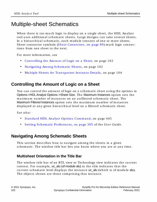
LO
HDL Analyst Tool Multiple-sheet Schematics
© 2021 Synopsys, Inc. Synplify Pro for Microchip Edition Reference Manual102 Synopsys Confidential Information February 2021
Multiple-sheet SchematicsWhen there is too much logic to display on a single sheet, the HDL Analyst tool uses additional schematic sheets. Large designs can take several sheets. In a hierarchical schematic, each module consists of one or more sheets. Sheet connector symbols (Sheet Connectors, on page 89) mark logic connec-tions from one sheet to the next.
For more information, see
• Controlling the Amount of Logic on a Sheet, on page 102
• Navigating Among Schematic Sheets, on page 102
• Multiple Sheets for Transparent Instance Details, on page 104
Controlling the Amount of Logic on a SheetYou can control the amount of logic on a schematic sheet using the options in Options->HDL Analyst Options->Sheet Size. The Maximum Instances option sets the maximum number of instances on an unfiltered schematic sheet. The Maximum Filtered Instances option sets the maximum number of instances displayed at any given hierarchical level on a filtered schematic sheet.
See also:
• Standard HDL Analyst Options Command, on page 445
• Setting Schematic Preferences, on page 305 of the User Guide.
Navigating Among Schematic SheetsThis section describes how to navigate among the sheets in a given schematic. The window title bar lets you know where you are at any time.
Multisheet Orientation in the Title BarThe window title bar of an RTL view or Technology view indicates the current context. For example, uc_alu (of module alu) in the title indicates that the current schematic level displays the instance uc_alu (which is of module alu). The objects shown are those comprising that instance.
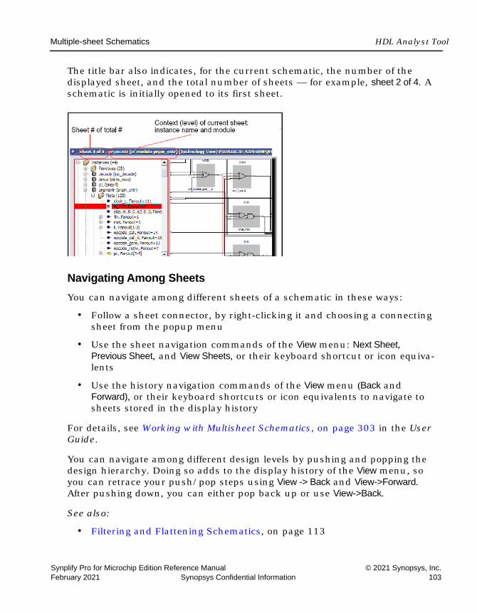
Multiple-sheet Schematics HDL Analyst Tool
Synplify Pro for Microchip Edition Reference Manual © 2021 Synopsys, Inc.February 2021 Synopsys Confidential Information 103
The title bar also indicates, for the current schematic, the number of the displayed sheet, and the total number of sheets — for example, sheet 2 of 4. A schematic is initially opened to its first sheet.
Navigating Among SheetsYou can navigate among different sheets of a schematic in these ways:
• Follow a sheet connector, by right-clicking it and choosing a connecting sheet from the popup menu
• Use the sheet navigation commands of the View menu: Next Sheet, Previous Sheet, and View Sheets, or their keyboard shortcut or icon equiva-lents
• Use the history navigation commands of the View menu (Back and Forward), or their keyboard shortcuts or icon equivalents to navigate to sheets stored in the display history
For details, see Working with Multisheet Schematics, on page 303 in the User Guide.
You can navigate among different design levels by pushing and popping the design hierarchy. Doing so adds to the display history of the View menu, so you can retrace your push/pop steps using View -> Back and View->Forward. After pushing down, you can either pop back up or use View->Back.
See also:
• Filtering and Flattening Schematics, on page 113

LO
HDL Analyst Tool Multiple-sheet Schematics
© 2021 Synopsys, Inc. Synplify Pro for Microchip Edition Reference Manual104 Synopsys Confidential Information February 2021
• View Menu: RTL and Technology Views Commands, on page 326
• Pushing and Popping Hierarchical Levels, on page 105
Multiple Sheets for Transparent Instance DetailsThe details of a transparent instance in a filtered view are drawn in two ways:
• Generally, these interior details are spread out over multiple sheets at the same schematic level (module) as the instance that contains them. You navigate these sheets as usual, using the methods described in Navigating Among Schematic Sheets, on page 102.
• If the number of nested contents exceeds the limit set with the Filtered Instances option (Options->HDL Analyst Options), the nested contents are drawn on separate sheets. The parent hierarchical instance is empty, with a notation (for example, Go to sheets 4-16) inside it, indicating which sheets contain its lower-level details. You access the sheets containing the lower-level details using the sheet navigation commands of the View menu, such as Next Sheet.
See also:
• Controlling the Amount of Logic on a Sheet, on page 102
• View Menu: RTL and Technology Views Commands, on page 326

Exploring Design Hierarchy HDL Analyst Tool
Synplify Pro for Microchip Edition Reference Manual © 2021 Synopsys, Inc.February 2021 Synopsys Confidential Information 105
Exploring Design HierarchyThe hierarchy in your design can be explored in different ways. The following sections explain how to move between hierarchical levels:
• Pushing and Popping Hierarchical Levels, on page 105
• Navigating With a Hierarchy Browser, on page 109
• Looking Inside Hierarchical Instances, on page 110
Pushing and Popping Hierarchical LevelsYou can navigate your design hierarchy by pushing down into a high-level schematic object or popping back up. Pushing down into an object takes you to a lower-level schematic that shows the internal logic of the object. Popping up from a lower level brings you back to the parent higher-level object.
Pushing and popping is best suited for traversing the hierarchy of a specific object. If you want a more general view of your design hierarchy, use the Hierarchy Browser instead. See Navigating With a Hierarchy Browser, on page 109 and Looking Inside Hierarchical Instances, on page 110 for other ways of viewing design hierarchy.
Pushable Schematic ObjectsTo push into an instance, it must have hierarchy. You can push into the object regardless of its position in the design hierarchy; for example, you can push into the object if it is shown nested inside a transparent instance. You can push down into the following kinds of schematic objects:
• Non-hidden hierarchical instances. To push into a hidden instance, unhide it first.
• Technology-specific primitives (not logic primitives)
• Inferred ROMs and state machines in RTL views. Inferred ROMs, RAMs, and state machines do not appear in Technology views, because they are resolved into technology-specific primitives.

LO
HDL Analyst Tool Exploring Design Hierarchy
© 2021 Synopsys, Inc. Synplify Pro for Microchip Edition Reference Manual106 Synopsys Confidential Information February 2021
When you push/pop, the HDL Analyst window displays the appropriate level of design hierarchy, except in the following cases:
• In the Synplify Pro tool, the FSM Viewer opens, with graphical informa-tion about the FSM. See the FSM Viewer Window, on page 83, for more information.
• When you push into an inferred ROM in an RTL view, the Text Editor window opens and displays the ROM data table (rom.info file).
You can use the following indicators to determine whether you can push into an object:
• The mouse pointer shape when Push/Pop mode is enabled. See How to Push and Pop Hierarchical Levels, on page 106 for details.
• A small H symbol ( ) in the lower left corner indicates a hidden instance, and you cannot push into it.
• The Hierarchy Browser symbols indicates the type of instance and you can use that to determine whether you can push into an object. For example, hierarchical instance ( ), technology-specific primitive ( ), logic primitive such as XOR ( ), or other primitive instance ( ). The browser symbol does not indicate whether or not an instance is hidden.
• The status bar at the bottom of the main synthesis tool window reports information about the object under the pointer, including whether or not it is a hidden instance or a primitive.
How to Push and Pop Hierarchical LevelsYou push/pop design levels with the HDL Analyst Push/Pop mode. To enable or disable this mode, toggle View->Push/Pop Hierarchy, use the icon, or use the appropriate mouse strokes.

Exploring Design Hierarchy HDL Analyst Tool
Synplify Pro for Microchip Edition Reference Manual © 2021 Synopsys, Inc.February 2021 Synopsys Confidential Information 107
Once Push/Pop mode is enabled, you push or pop as follows:
• To pop, place the pointer in an empty area of the schematic background, then click or use the appropriate mouse stroke. The background area inside a transparent instance acts just like the background area outside the instance.
• To push into an object, place the mouse pointer over the object and click or use the appropriate mouse stroke. To push into a transparent instance, place the pointer over its pale yellow border, not its hollow (white) interior. Pushing into an object nested inside a transparent hierarchical instance descends to a lower level than pushing into the enclosing transparent instance. In the following figure, pushing into transparent instance inst2 descends one level; pushing into nested instance inst2.II_3 descends two levels.

LO
HDL Analyst Tool Exploring Design Hierarchy
© 2021 Synopsys, Inc. Synplify Pro for Microchip Edition Reference Manual108 Synopsys Confidential Information February 2021
The following arrow mouse pointers indicate status in Push/Pop mode. For other indicators, see Pushable Schematic Objects, on page 105.
See also:
• Hidden Hierarchical Instances, on page 93
• Transparent and Opaque Display of Hierarchical Instances, on page 91
• Using Mouse Strokes, on page 53
• Navigating With a Hierarchy Browser, on page 109
A down arrow Indicates that you can push (descend) into the object under the pointer and view its details at the next lower level.
An up arrow Indicates that there is a hierarchical level above the current sheet.
A crossed-out double arrow
Indicates that there is no accessible hierarchy above or below the current pointer position. If the pointer is over the schematic background it indicates that the current level is the top and you cannot pop higher. If the pointer is over an object, the object is an object you cannot push into: a non-hierarchical instance, a hidden hierarchical instance, or a black box.
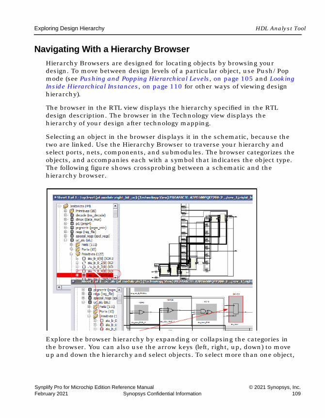
Exploring Design Hierarchy HDL Analyst Tool
Synplify Pro for Microchip Edition Reference Manual © 2021 Synopsys, Inc.February 2021 Synopsys Confidential Information 109
Navigating With a Hierarchy BrowserHierarchy Browsers are designed for locating objects by browsing your design. To move between design levels of a particular object, use Push/Pop mode (see Pushing and Popping Hierarchical Levels, on page 105 and Looking Inside Hierarchical Instances, on page 110 for other ways of viewing design hierarchy).
The browser in the RTL view displays the hierarchy specified in the RTL design description. The browser in the Technology view displays the hierarchy of your design after technology mapping.
Selecting an object in the browser displays it in the schematic, because the two are linked. Use the Hierarchy Browser to traverse your hierarchy and select ports, nets, components, and submodules. The browser categorizes the objects, and accompanies each with a symbol that indicates the object type. The following figure shows crossprobing between a schematic and the hierarchy browser.
Explore the browser hierarchy by expanding or collapsing the categories in the browser. You can also use the arrow keys (left, right, up, down) to move up and down the hierarchy and select objects. To select more than one object,

LO
HDL Analyst Tool Exploring Design Hierarchy
© 2021 Synopsys, Inc. Synplify Pro for Microchip Edition Reference Manual110 Synopsys Confidential Information February 2021
press Ctrl and select the objects in the browser. To select a range of schematic objects, click an object at one end of the range, then hold the Shift key while clicking the name of an object at the other end of the range.
See also:
• Crossprobing Objects, on page 99
• Pushing and Popping Hierarchical Levels, on page 105
• Hierarchy Browser Popup Menu Commands, on page 483
Looking Inside Hierarchical InstancesAn alternative method of viewing design hierarchy is to examine transparent hierarchical instances (see Navigating With a Hierarchy Browser, on page 109 and Navigating With a Hierarchy Browser, on page 109 for other ways of viewing design hierarchy). A transparent instance appears as a hollow box with a pale yellow border. Inside this border are transparent and opaque objects from lower design levels.
Transparent instances provide design context. They show the lower-level logic nested within the transparent instance at the current design level, while pushing shows the same logic a level down. The following figure compares the same lower-level logic viewed in a transparent instance and a push operation:

Exploring Design Hierarchy HDL Analyst Tool
Synplify Pro for Microchip Edition Reference Manual © 2021 Synopsys, Inc.February 2021 Synopsys Confidential Information 111

LO
HDL Analyst Tool Exploring Design Hierarchy
© 2021 Synopsys, Inc. Synplify Pro for Microchip Edition Reference Manual112 Synopsys Confidential Information February 2021
You cannot control the display of transparent instances directly. However, you can perform the following operations, which result in the display of transparent instances:
• Hierarchically expand an object (using the expansion commands in the HDL Analyst menu).
• Dissolve selected hierarchical instances in a filtered schematic (HDL Analyst -> Dissolve Instances).
• Filter a schematic, after selecting multiple objects at more than one level. See Commands That Result in Filtered Schematics, on page 113 for additional information.
These operations only make non-hidden hierarchical instances transparent. You cannot dissolve hidden or primitive instances (including technology-specific primitives). However, you can do the following:
• Unhide hidden instances, then dissolve them.
• Push down into technology-specific primitives to see their lower-level details, and you can show the interiors of all technology-specific primi-tives.
See also:
• Pushing and Popping Hierarchical Levels, on page 105
• Navigating With a Hierarchy Browser, on page 109
• HDL Analyst Command, on page 414
• Transparent and Opaque Display of Hierarchical Instances, on page 91
• Hidden Hierarchical Instances, on page 93

Filtering and Flattening Schematics HDL Analyst Tool
Synplify Pro for Microchip Edition Reference Manual © 2021 Synopsys, Inc.February 2021 Synopsys Confidential Information 113
Filtering and Flattening SchematicsThis section describes the HDL Analyst commands that result in filtered and flattened schematics. It describes
• Commands That Result in Filtered Schematics, on page 113
• Combined Filtering Operations, on page 114
• Returning to The Unfiltered Schematic, on page 114
• Commands That Flatten Schematics, on page 115
• Selective Flattening, on page 116
• Filtering Compared to Flattening, on page 117
Commands That Result in Filtered SchematicsA filtered schematic shows a subset of your design. Any command that results in a filtered schematic is a filtering command. Some commands, like the Expand commands, increase the amount of logic displayed, but they are still considered filtering commands because they result in a filtered view of the design. Other commands like Filter Schematic and Isolate Paths remove objects from the current display.
Filtering commands include the following:
• Filter Schematic, Isolate Paths - reduce the displayed logic.
• Dissolve Instances (in a filtered schematic) - makes selected instances transparent.
• Expand, Expand to Register/Port, Expand Paths, Expand Inwards, Select Net Driver, Select Net Instances - display logic connected to the current selection.
• Show Critical Path, Flattened Critical Path, Hierarchical Critical Path - show critical paths.
All the filtering commands, except those that display critical paths, operate on the currently selected schematic object(s). The critical path commands operate on your entire design, regardless of what is currently selected.
All the filtering commands except Isolate Paths are accessible from the HDL Analyst menu; Isolate Paths is in the RTL view and Technology view popup menus (along with most of the other commands above).
LO
HDL Analyst Tool Filtering and Flattening Schematics
© 2021 Synopsys, Inc. Synplify Pro for Microchip Edition Reference Manual114 Synopsys Confidential Information February 2021
For information about filtering procedures, see Filtering Schematics, on page 340 in the User Guide.
See also:
• Filtered and Unfiltered Schematic Views, on page 85
• HDL Analyst Menu, on page 413 and RTL and Technology Views Popup Menus, on page 483
Combined Filtering OperationsFiltering operations are designed to be used in combination, successively. You can perform a sequence of operations like the following:
1. Use Filter Schematic to filter your design to examine a particular instance. See HDL Analyst Menu: Filtering and Flattening Commands, on page 416 for a description of the command.
2. Select Expand to expand from one of the output pins of the instance to add its immediate successor cells to the display. See HDL Analyst Menu: Hierarchical and Current Level Submenus, on page 414 for a description of the command.
3. Use Select Net Driver to add the net driver of a net connected to one of the successors. See HDL Analyst Menu: Hierarchical and Current Level Submenus, on page 414 for a description of the command.
4. Use Isolate Paths to isolate the net driver instance, along with any of its connecting paths that were already displayed. See HDL Analyst Menu: Analysis Commands, on page 420 for a description of the command.
Filtering operations add their resulting filtered schematics to the history of schematic displays, so you can use the View menu Forward and Back commands to switch between the filtered views. You can also combine filtering with the search operation. See Finding Schematic Objects, on page 97 for more information.
Returning to The Unfiltered SchematicA filtered schematic often loses the design context, as it is removed from the display by filtering. After a series of multiple or complex filtering operations, you might want to view the context of a selected object. You can do this by
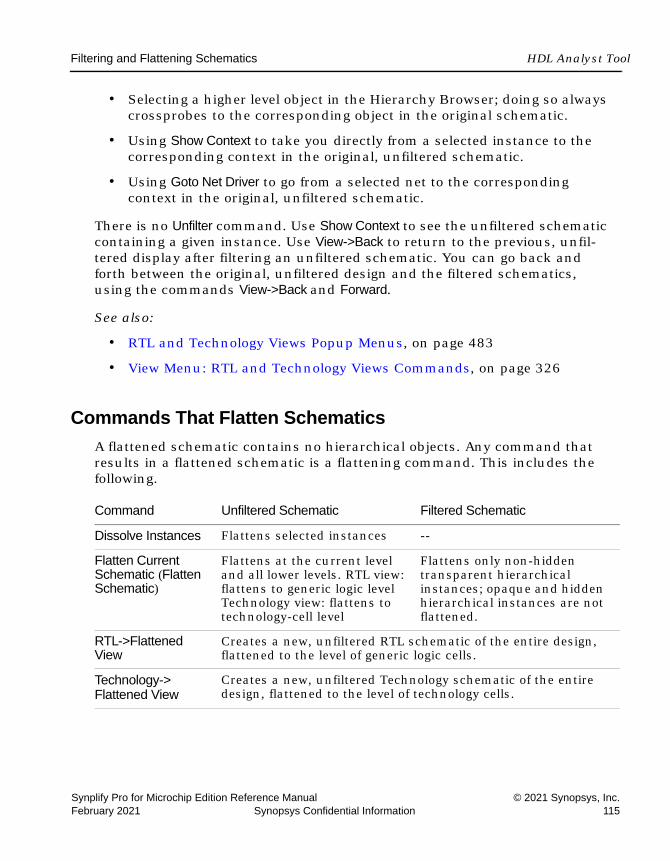
Filtering and Flattening Schematics HDL Analyst Tool
Synplify Pro for Microchip Edition Reference Manual © 2021 Synopsys, Inc.February 2021 Synopsys Confidential Information 115
• Selecting a higher level object in the Hierarchy Browser; doing so always crossprobes to the corresponding object in the original schematic.
• Using Show Context to take you directly from a selected instance to the corresponding context in the original, unfiltered schematic.
• Using Goto Net Driver to go from a selected net to the corresponding context in the original, unfiltered schematic.
There is no Unfilter command. Use Show Context to see the unfiltered schematic containing a given instance. Use View->Back to return to the previous, unfil-tered display after filtering an unfiltered schematic. You can go back and forth between the original, unfiltered design and the filtered schematics, using the commands View->Back and Forward.
See also:
• RTL and Technology Views Popup Menus, on page 483
• View Menu: RTL and Technology Views Commands, on page 326
Commands That Flatten SchematicsA flattened schematic contains no hierarchical objects. Any command that results in a flattened schematic is a flattening command. This includes the following.
Command Unfiltered Schematic Filtered Schematic
Dissolve Instances Flattens selected instances --
Flatten Current Schematic (Flatten Schematic)
Flattens at the current level and all lower levels. RTL view: flattens to generic logic level Technology view: flattens to technology-cell level
Flattens only non-hidden transparent hierarchical instances; opaque and hidden hierarchical instances are not flattened.
RTL->Flattened View
Creates a new, unfiltered RTL schematic of the entire design, flattened to the level of generic logic cells.
Technology-> Flattened View
Creates a new, unfiltered Technology schematic of the entire design, flattened to the level of technology cells.
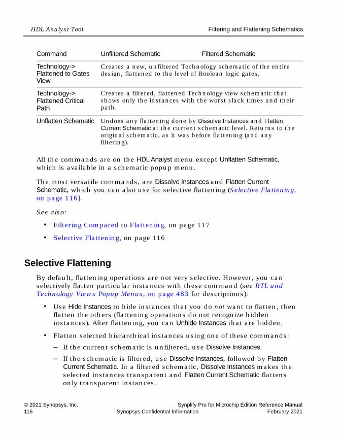
LO
HDL Analyst Tool Filtering and Flattening Schematics
© 2021 Synopsys, Inc. Synplify Pro for Microchip Edition Reference Manual116 Synopsys Confidential Information February 2021
All the commands are on the HDL Analyst menu except Unflatten Schematic, which is available in a schematic popup menu.
The most versatile commands, are Dissolve Instances and Flatten Current Schematic, which you can also use for selective flattening (Selective Flattening, on page 116).
See also:
• Filtering Compared to Flattening, on page 117
• Selective Flattening, on page 116
Selective FlatteningBy default, flattening operations are not very selective. However, you can selectively flatten particular instances with these command (see RTL and Technology Views Popup Menus, on page 483 for descriptions):
• Use Hide Instances to hide instances that you do not want to flatten, then flatten the others (flattening operations do not recognize hidden instances). After flattening, you can Unhide Instances that are hidden.
• Flatten selected hierarchical instances using one of these commands:
– If the current schematic is unfiltered, use Dissolve Instances.– If the schematic is filtered, use Dissolve Instances, followed by Flatten
Current Schematic. In a filtered schematic, Dissolve Instances makes the selected instances transparent and Flatten Current Schematic flattens only transparent instances.
Technology-> Flattened to Gates View
Creates a new, unfiltered Technology schematic of the entire design, flattened to the level of Boolean logic gates.
Technology-> Flattened Critical Path
Creates a filtered, flattened Technology view schematic that shows only the instances with the worst slack times and their path.
Unflatten Schematic Undoes any flattening done by Dissolve Instances and Flatten Current Schematic at the current schematic level. Returns to the original schematic, as it was before flattening (and any filtering).
Command Unfiltered Schematic Filtered Schematic
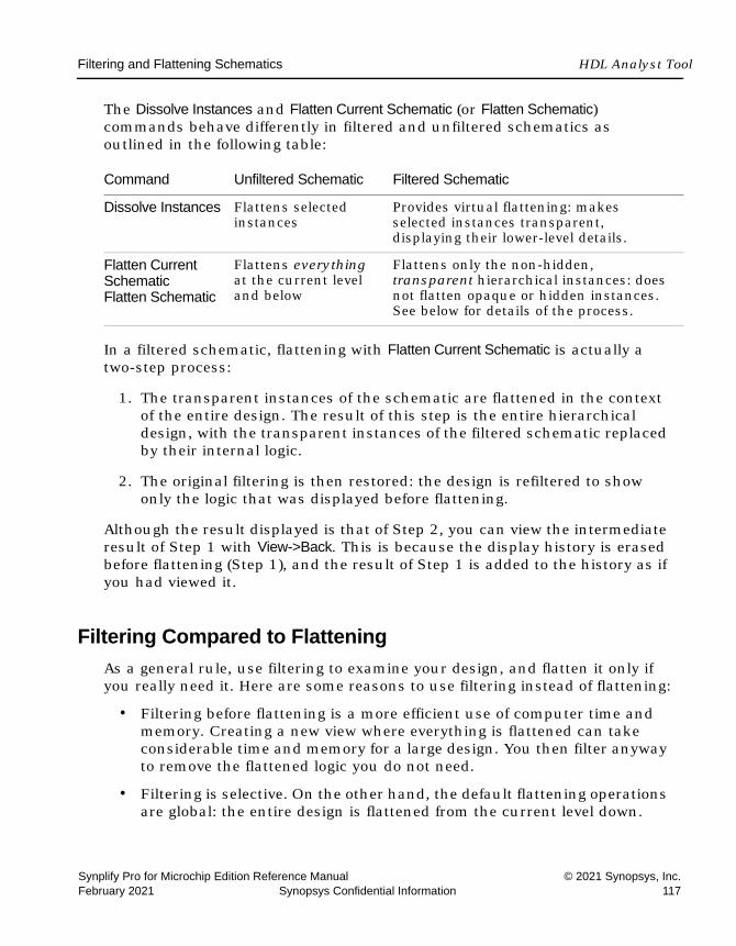
Filtering and Flattening Schematics HDL Analyst Tool
Synplify Pro for Microchip Edition Reference Manual © 2021 Synopsys, Inc.February 2021 Synopsys Confidential Information 117
The Dissolve Instances and Flatten Current Schematic (or Flatten Schematic) commands behave differently in filtered and unfiltered schematics as outlined in the following table:
In a filtered schematic, flattening with Flatten Current Schematic is actually a two-step process:
1. The transparent instances of the schematic are flattened in the context of the entire design. The result of this step is the entire hierarchical design, with the transparent instances of the filtered schematic replaced by their internal logic.
2. The original filtering is then restored: the design is refiltered to show only the logic that was displayed before flattening.
Although the result displayed is that of Step 2, you can view the intermediate result of Step 1 with View->Back. This is because the display history is erased before flattening (Step 1), and the result of Step 1 is added to the history as if you had viewed it.
Filtering Compared to FlatteningAs a general rule, use filtering to examine your design, and flatten it only if you really need it. Here are some reasons to use filtering instead of flattening:
• Filtering before flattening is a more efficient use of computer time and memory. Creating a new view where everything is flattened can take considerable time and memory for a large design. You then filter anyway to remove the flattened logic you do not need.
• Filtering is selective. On the other hand, the default flattening operations are global: the entire design is flattened from the current level down.
Command Unfiltered Schematic Filtered Schematic
Dissolve Instances Flattens selected instances
Provides virtual flattening: makes selected instances transparent, displaying their lower-level details.
Flatten Current SchematicFlatten Schematic
Flattens everything at the current level and below
Flattens only the non-hidden, transparent hierarchical instances: does not flatten opaque or hidden instances. See below for details of the process.

LO
HDL Analyst Tool Filtering and Flattening Schematics
© 2021 Synopsys, Inc. Synplify Pro for Microchip Edition Reference Manual118 Synopsys Confidential Information February 2021
Similarly, the inverse operation (UnFlatten Schematic) unflattens every-thing on the current schematic level.
• Flattening operations eliminate the history for the current view: You can not use View->Back after flattening. (You can, however, use UnFlatten Schematic to regenerate the unflattened schematic.).
See also:
• RTL and Technology Views Popup Menus, on page 483
• Selective Flattening, on page 116
Timing Information and Critical Paths HDL Analyst Tool
Synplify Pro for Microchip Edition Reference Manual © 2021 Synopsys, Inc.February 2021 Synopsys Confidential Information 119
Timing Information and Critical PathsThe HDL Analyst tool provides several ways of examining critical paths and timing information, to help you analyze problem areas. The different ways are described in the following sections.
• Timing Reports, on page 119
• Critical Paths and the Slack Margin Parameter, on page 120
• Examining Critical Path Schematics, on page 121
See the following for more information about timing and result analysis:
• Watch Window, on page 37
• Log File, on page 157
• Chapter 13, Optimizing Processes for Productivity in the User Guide
Timing ReportsWhen you synthesize a design, a default timing report is automatically written to the log file, which you can view using View->View Log File. This report provides a clock summary, I/O timing summary, and detailed timing infor-mation for your design.
For certain device technologies, you can use the Analysis->Timing Analyst command to generate a custom timing report. Use this command to specify start and end points of paths whose timing interests you, and set a limit for the number of paths to analyze between these points. By default, the sequen-tial instances, input ports, and output ports that are currently selected in the Technology views of the design are the candidates for choosing start and end points. In addition, the start and end points of the previous Timing Analyst run become the default start and end points for the next run. When analyzing timing, any latches in the path are treated as level-sensitive registers.
The custom timing report is stored in a text file named resultsfile.ta, where resultsfile is the name of the results file (see Implementation Results Panel, on page 353). In addition, a corresponding output netlist file is generated, named resultsfile_ta.srm. Both files are in the implementation results direc-tory.

LO
HDL Analyst Tool Timing Information and Critical Paths
© 2021 Synopsys, Inc. Synplify Pro for Microchip Edition Reference Manual120 Synopsys Confidential Information February 2021
The Timing Analyst dialog box provides check boxes for viewing the text report (Open Report) in the Text Editor and the corresponding netlist (Open Schematic) in a Technology view. This Technology view of the timing path, labeled Timing View in the title bar, is special in two ways:
• The Timing View shows only the paths you specify in the Timing Analyst dialog box. It corresponds to a special design netlist that contains critical timing data.
• The Timing Analyst and Show Critical Path commands (and equivalent icons and shortcuts) are unavailable whenever the Timing View is active.
See also:
• Analysis Menu, on page 401
• Timing Reports, on page 162
• Log File, on page 157
Critical Paths and the Slack Margin ParameterThe HDL Analyst tool can isolate critical paths in your design, so that you can analyze problem areas, add timing constraints where appropriate, and resyn-thesize for better results.
After you successfully run synthesis, you can display just the critical paths of your design using any of the following commands from the HDL Analyst menu:
• Hierarchical Critical Path
• Flattened Critical Path
• Show Critical Path
The first two commands create a new Technology view, hierarchical or flattened, respectively. The Show Critical Path command reuses the current Technology view. Neither the current selection nor the current sheet display have any effect on the result. The result is flat if the entire design was already flat; otherwise it is hierarchical. Use Show Critical Path if you want to maintain the existing display history.
All these commands filter your design to show only the instances (and their paths) with the worst slack times. They also enable HDL Analyst -> Show Timing Information, displaying timing information.
Timing Information and Critical Paths HDL Analyst Tool
Synplify Pro for Microchip Edition Reference Manual © 2021 Synopsys, Inc.February 2021 Synopsys Confidential Information 121
Negative slack times indicate that your design has not met its timing require-ments. The worst (most negative) slack time indicates the amount by which delays in the critical path cause the timing of the design to fail. You can also obtain a range of worst slack times by setting the slack margin parameter to control the sensitivity of the critical-path display. Instances are displayed only if their slack times are within the slack margin of the (absolutely) worst slack time of the design.
The slack margin is the criterion for distinguishing worst slack times. The larger the margin, the more relaxed the measure of worst, so the greater the number of critical-path instances displayed. If the slack margin is zero (the default value), then only instances with the worst slack time of the design are shown. You use HDL Analyst->Set Slack Margin to change the slack margin.
The critical-path commands do not calculate a single critical path. They filter out instances whose slack times are not too bad (as determined by the slack margin), then display the remaining, worst-slack instances, together with their connecting paths.
For example, if the worst slack time of your design is -10 ns and you set a slack margin of 4 ns, then the critical path commands display all instances with slack times between -6 ns and -10 ns.
See also:
• HDL Analyst Menu, on page 413
• HDL Analyst Command, on page 414
• Handling Negative Slack, on page 364 of the User Guide
• Analyzing Timing in Schematic Views, on page 358 of the User Guide
Examining Critical Path SchematicsUse successive filtering operations to examine different aspects of the critical path. After filtering, use View -> Back to return to the previous point, then filter differently. For example, you could use the command Isolate Paths to examine the cone of logic from a particular pin, then use the Back command to return to the previous display, then use Isolate Paths on a different pin to examine a different logic cone, and so on.

LO
HDL Analyst Tool Timing Information and Critical Paths
© 2021 Synopsys, Inc. Synplify Pro for Microchip Edition Reference Manual122 Synopsys Confidential Information February 2021
Also, the Show Context and Goto Net Driver commands are particularly useful after you have done some filtering. They let you get back to the original, unfil-tered design, putting selected objects in context.
See also:
• Returning to The Unfiltered Schematic, on page 114
• Filtering and Flattening Schematics, on page 113

Synplify Pro for Microchip Edition Reference Manual © 2021 Synopsys, Inc.February 2021 Synopsys Confidential Information 123
C H A P T E R 4
Constraint Guidelines
Constraints are used in the FPGA synthesis environment to achieve optimal design results. Timing constraints set performance goals, non-timing constraints (design constraints) guide the tool through optimizations that further enhance performance.
This chapter provides an overview of how constraints are handled in the FPGA synthesis environment.
• Constraint Types, on page 124
• Constraint Files, on page 125
• Timing Constraints, on page 127
• FDC Constraints, on page 130
• Methods for Creating Constraints, on page 131
• Constraint Translation, on page 133
• Constraint Checking, on page 138
• Database Object Search, on page 140
• Forward Annotation, on page 141
• Auto Constraints, on page 141

LO
Constraint Guidelines Constraint Types
© 2021 Synopsys, Inc. Synplify Pro for Microchip Edition Reference Manual124 Synopsys Confidential Information February 2021
Constraint Types One way to ensure the FPGA synthesis tool achieves the best quality of results for your design is to define proper constraints. In the FPGA environ-ment, constraints can be categorized by the following types:
The easiest way to specify constraints is through the SCOPE interface. The tool saves timing and design constraints to an FDC file that you add to your project.
See Also
Type Description
Timing Performance constraints that guide the synthesis tools to achieve optimal results. Examples: clocks (create_clock), clock groups (set_clock_groups), and timing exceptions like multicycle and false paths (set_multicycle_path...)See Timing Constraints , on page 127 for information on defining these constraints.
Design Additional design goals that enhance or guide tool optimizations. Examples: Attributes and directives (define_attribute, define_global_attribute), I/O standards (define_io_standard), and compile points (define_compile_point).
Constraint Files , on page 125 Overview of constraint files
Timing Constraints , on page 127 Overview of timing constraint definitions and FDC file generation.
SCOPE Constraints Editor , on page 216
Information about automatic generation of timing and design constraints.
Timing Constraints , on page 262 Timing constraint syntax
Design Constraints , on page 301 Design constraint syntax

Constraint Files Constraint Guidelines
Synplify Pro for Microchip Edition Reference Manual © 2021 Synopsys, Inc.February 2021 Synopsys Confidential Information 125
Constraint FilesThe figure below shows the files used for specifying various types of constraints. The FDC file is the most important one and is the primary file for both timing and non-timing design constraints. The other constraint files are used for specific features or as input files to generate the FDC file, as described in Timing Constraints, on page 127. The figure also indicates the specific processes controlled by attributes and directives.

LO
Constraint Guidelines Constraint Files
© 2021 Synopsys, Inc. Synplify Pro for Microchip Edition Reference Manual126 Synopsys Confidential Information February 2021
The table is a summary of the various kinds of constraint files.
File Type Common Commands Comments
FDC Timing constraints
create_clock, set_multicycle_delay …
Used for synthesis. Includes timing constraints that follow the Synopsys standard format as well as design constraints.
Design constraints
define_attribute, define_io_standard …
ADC Timing constraints for timing analysis
create_clock, set_multicycle_delay …
Used with the stand-alone timing analyzer.
SDC (Synopsys Standard)
FPGA timing constraints
create_clock,set_clock_latency,set_false_path …
Use sdc2fdc to convert constraints to an FDC file so that they can be passed to the synthesis tools.
SDC(Legacy)
Legacy timing constraints and non-timing (or design) constraints
define_clock, define_false_path define_attribute, define_collection …
Use sdc2fdc to convert the constraints to an FDC file so that they can be passed to the synthesis tools.
Timing Constraints Constraint Guidelines
Synplify Pro for Microchip Edition Reference Manual © 2021 Synopsys, Inc.February 2021 Synopsys Confidential Information 127
Timing ConstraintsThe synthesis tool has supported different timing formats in the past, and this section describes some of the details of standardization:
• Legacy SDC and Synopsys Standard SDC, on page 127
• FDC File Generation, on page 128
• Timing Constraint Precedence in Mixed Constraint Designs, on page 128
Legacy SDC and Synopsys Standard SDCReleases prior to G-2012.09 had two types of constraint files that could be used in a design project:
• Legacy “Synplify-style” timing constraints (define_clock, define_false_path...) saved to an sdc file. This file also included non-timing design constraints, like attributes and compile points.
• Synopsys standard timing constraints (create_clock, set_false_path...). These constraints were also saved to an sdc file, which only contained timing constraints. Non-timing constraints were in a separate sdc file. The tool used the two files together, drawing timing constraints from one and non-timing constraints from the other.
Starting with the G-2012.09 release, Synopsys standard timing constraint format has replaced the legacy-style constraint format, and a new FDC (FPGA design constraint) file consolidates both timing and design formats. As a result of these updates, there are some changes in the use model:
• Timing constraints in the legacy format are converted and included in an FDC file, which includes both timing and non-timing constraints. The file uses the Synopsys standard syntax for timing constraints (create_-clock, set_multicycle_path...). The syntax for non-timing design constraints is unchanged (define_attribute, define_io_standard...).
• The SCOPE editor has been enhanced to support the timing constraint changes, so that new constraints can be entered correctly.
• For older designs, use the sdc2fdc command to do a one-time conversion.

LO
Constraint Guidelines Timing Constraints
© 2021 Synopsys, Inc. Synplify Pro for Microchip Edition Reference Manual128 Synopsys Confidential Information February 2021
FDC File GenerationThe following figure is a simplified summary of constraint-file handling and the generation of fdc.
It is not required that you convert Synopsys standard sdc constraints as the figure implies, because they are already in the correct format. You could have a design with mixed constraints, with separate Synopsys standard sdc and fdc files. The disadvantage to keeping them in the standard sdc format is that you cannot view or edit the constraints through the SCOPE interface.
Timing Constraint Precedence in Mixed Constraint DesignsYour design could include timing constraints in a Synopsys standard sdc file and others in an fdc file. With mixed timing constraints in the same design, the following order of precedence applies:
Timing Constraints Constraint Guidelines
Synplify Pro for Microchip Edition Reference Manual © 2021 Synopsys, Inc.February 2021 Synopsys Confidential Information 129
The tool reads the file order listed in the project file and any conflicting constraint overwrites a previous constraint. This means that constraint priority is determined by the constraint that is read last.
With the legacy timing constraints, it is strongly recommended that you convert them to the fdc format. However, even if you retain the old format in an existing design, they must be used alone and cannot be mixed in the same design as fdc or Synopsys standard timing sdc constraints. Specifically, do not specify timing constraints using mixed formats. For example, do not define clocks with define_clock and create_clock together in the same constraint file or multiple SDC/FDC files.
For the list of FPGA timing constraints (FDC) and their syntax, see Timing Constraints, on page 262.

LO
Constraint Guidelines FDC Constraints
© 2021 Synopsys, Inc. Synplify Pro for Microchip Edition Reference Manual130 Synopsys Confidential Information February 2021
FDC ConstraintsThe FPGA design constraints (FDC) file contains constraints that the tool uses during synthesis. This FDC file includes both timing constraints and non-timing constraints in a single file.
• Timing constraints define performance targets to achieve optimal results. The constraints follow the Synopsys standard format, such as create_clock, set_input_delay, and set_false_path.
• Non-timing (or design constraints) define additional goals that help the tool optimize results. These constraints are unique to the FPGA synthesis tools and include constraints such as define_attribute, define_io_-standard, and define_compile_point.
The recommended method to define constraints is to enter them in the SCOPE editor, and the tool automatically generates the appropriate syntax. If you define constraints manually, use the appropriate syntax for each type of constraint (timing or non-timing), as described above. See Methods for Creating Constraints, on page 131 for details on generating constraint files.
Prior to release G-2012.09, designs used timing constraints in either legacy Synplify-style format or Synopsys standard format. You must do a one-time conversion on any existing SDC files to convert them to FDC files using the following command:
% sdc2fdc sdc2fdc converts constraints as follows:
Once defined, the FDC file can be added to your project. Double-click this file from the Project view to launch the SCOPE editor to view and/or modify your constraints. See Converting SDC to FDC, on page 164 for details on how to run sdc2fdc.
For legacy Synplify-style timing constraints
Converts timing constraints to Synopsys standard format and saves them to an FDC file.
For Synopsys standard timing constraints
Preserves Synopsys standard format timing constraints and saves them to an FDC file.
For non-timing or design constraints
Preserves the syntax for these constraints and saves them to an FDC file.

Methods for Creating Constraints Constraint Guidelines
Synplify Pro for Microchip Edition Reference Manual © 2021 Synopsys, Inc.February 2021 Synopsys Confidential Information 131
Methods for Creating ConstraintsConstraints are passed to the synthesis environment in FDC files using Tcl command syntax.
New DesignsFor new designs, you can specify constraints using any of the following methods:
Definition Method Description
SCOPE Editor(fdc file)–Recommended
Use this method to specify constraints wherever possible. The SCOPE editor automatically generates fdc constraints with the right syntax. You can use it for most constraints. See Chapter 4, Constraint Commands, for information how to use SCOPE to automatically generate constraint syntax.Access: File->New->FPGA Design Constraints …
Manually-Entered Text Editor(fdc File, all other constraint files)
You can manually enter constraints in a text file. Make sure to use the correct syntax for the timing and design commands. The SCOPE GUI includes a TCL View with an advanced text editor, where you can manually generate the constraint syntax. For a description of this view, see TCL View , on page 240.You can also open any constraint file in a text editor to modify it.
Source Code Attributes/Directives(HDL files)
Directives must be entered in the source code because they affect the compiler. Do not include any other constraints in the source code, as this makes the source code less portable. In addition, you must recompile the design for the constraints to take effect.Attributes can be entered through the SCOPE interface, as they affect the mapper, not the compiler
Automatic— First Pass Enable the Auto Constrain button in the Project view to have the tool automatically generate constraints based on inferred clocks. See Using Auto Constraints , on page 376 in the User Guide for details.Use this method as a quick first pass to get an idea of what constraints can be set.

LO
Constraint Guidelines Methods for Creating Constraints
© 2021 Synopsys, Inc. Synplify Pro for Microchip Edition Reference Manual132 Synopsys Confidential Information February 2021
If there are multiple timing exception constraints on the same object, the software uses the guidelines described in Conflict Resolution for Timing Excep-tions, on page 258 to determine the constraint that takes precedence.
See AlsoTo specify the correct syntax for the timing and design commands, see:
• Chapter 4, Constraint Commands
• Attribute Reference Manual
Existing DesignsThe SCOPE editor in this release does not save constraints to SDC files. For designs prior to G-2012.09, it is recommended that you migrate your timing constraints to FDC format to take advantage of the tool’s enhanced handling of these types of constraints. To migrate constraints, use the sdc2fdc command (see Converting SDC to FDC, on page 164l) on your sdc files.
Note: If you need to edit an SDC file, either use a text editor, or double-click the file to open the legacy SCOPE editor. For infor-mation on editing older SDC files, see Using the SCOPE Editor (Legacy), on page 165.
See AlsoTo use the current SCOPE editor, see:
• Chapter 4, Constraint Commands
• Chapter 5, Specifying Constraints
Constraint Translation Constraint Guidelines
Synplify Pro for Microchip Edition Reference Manual © 2021 Synopsys, Inc.February 2021 Synopsys Confidential Information 133
Constraint TranslationThe tool includes standalone scripts to convert specific vendor constraints, as well as functionality that includes constraint translation as part of the larger task of generating a synthesis project from vendor files.
sdc2fdc ConversionThe sdc2fdc Tcl shell command translates legacy FPGA timing constraints to Synopsys FPGA timing constraints. This command scans the input SDC files and attempts to convert constraints for the implementation.
For details, see the following:
• Troubleshooting Conversion Error Messages, on page 133
• sdc2fdc FPGA Design Constraint (FDC) File, on page 135
• sdc2fdc, on page 111 in the Command Reference manual (syntax)
Troubleshooting Conversion Error MessagesThe following table contains common error messages you might encounter when running the sdc2fdc Tcl shell command, and descriptions of how to resolve these problems. In addition to these messages, you must also ensure that your files have read/write permissions set properly and that there is sufficient disk space.
Message Example Underlying Problem
Remove/disable D:FDC_constraints/rev_FDC/top_translated.fdc from the current implementation.
Cannot translate a *_translated.fdc file
Add/enable one or more SDC constraint files. No active constraint files
Add clock object qualifier (p: n: ...) for"define_clock -name {clka {clka} -period 10 -clockgroup {default_clkgroup_0}" Synplicity_SDC source file: D:.../clk_prior/scratch/top.sdc. Line number: 32
Clock not translated

LO
Constraint Guidelines Constraint Translation
© 2021 Synopsys, Inc. Synplify Pro for Microchip Edition Reference Manual134 Synopsys Confidential Information February 2021
Fix any issues in the SDC source file and rerun the sdc2fdc command.
Batch ModeIf you run sdc2fdc -batch, then the following occurs:
• The two Clock not translated messages in the table above are not generated.
• When the translation is successful, the SDC file is disabled and the FDC file is enabled and saved automatically in the project file.
However, if the -batch option is not used and the translation is successful, then the SDC file is disabled and the FDC file is enabled but
Specify -name for "define_clock {p:clkb} -period 20 -clockgroup {default_clkgroup_1}" Synplicity SDC source file: D:.../clk_prior/scratch/top.sdc. Line number: 33
Clock not translated
Missing qualifier(s) (i: p: n: ...) "define_multicycle_path 4 -from {a* b*} -to $fdc_cmd_0 -start"Synplicity SDC source file: D:.../clk_prior/scratch/top.sdc. Line number: 76
Bad -from list for define_multicycle_path {a* b*}
Mixing of object types not permitted "define_multicycle_path -to {i:*y*.q[*] p:ena} 3" Synplicity SDC source file: D:.../clk_prior/scratch/top.sdc. Line number: 77
Bad -to list for define_multicycle_path {i: *y* .q[*] p:ena}
Mixing of object types and missing qualifiers not permitted "define_multicycle_path -from {i:*y*.q[*] p:ena enab} 3" Synplicity SDC source file:D:.../clk_prior/scratch/top.sdc. Line number: 77
Bad -from list for define_multicycle_path {i:*y* .q[*] p:ena enab}
Default 1000. "create_clock -name {clkb} {p:clkb} -period 1000 -waveform {0 500.0}" Synplicity SDC source file:D:.../clk_prior/scratch/top.sdc. Line number: 33
No period or frequency found
"create_clock -name {clka} {p:clka} -period 10 -rise 5-clockgroup {default_clkgroup_0" Synplicity SDC source file:D:.../clk_prior/scratch/top.sdc. Line number: 32
Must specify both -rise and -fall, or neither
Message Example Underlying Problem

Constraint Translation Constraint Guidelines
Synplify Pro for Microchip Edition Reference Manual © 2021 Synopsys, Inc.February 2021 Synopsys Confidential Information 135
not automatically saved in the Project file. A message to this effect displays in the Tcl shell window.
sdc2fdc FPGA Design Constraint (FDC) FileThe FDC constraint file generated after running sdc2fdc contains translated legacy FPGA timing constraints (SDC), which are now in the FDC format. This file is divided into two sections:
This file also provides the following:
• Each source sdc file has its separate subhead.
• Each compile point is treated as a top level, so its sdc file has its own _translated.fdc file.
• The translator adds the naming rule, set_rtl_ff_names, so that the synthesis tool knows these constraints are not from the Synopsys Design Compiler.
The following example shows the contents of the FDC file.
#################################################################################This file contains constraints from Synplicity SDC files that have been ####translated into Synopsys FPGA Design Constraints (FDC. ####Translated FDC output file: ####D:/bugs/timing_88/clk_prior/scratch/FDC_constraints/rev_2/top_translated.fdc ####Source SDC files to the translation: ####D:/bugs/timing_88/clk_prior/scratch/top.sdc #############################################################################
############################################################################# ####Source SDC file to the translation: ####D:/bugs/timing_88/clk_prior/scratch/top.sdc ##############################################################################Legacy constraint file #C:\Clean_Demos\Constraints_Training\top.sdc #Written on Mon May 21 15:58:35 2012 #by Synplify Pro, Synplify Pro Scope Editor # #Collections # define_scope_collection all_grp {define_collection \
1 Contains this information:• Valid FPGA design constraints (e.g. define_scope_collection and define_attribute) • Legacy timing constraints that were not translated because they were
specified with -disable.
2 Contains the legacy timing constraints that were translated.

LO
Constraint Guidelines Constraint Translation
© 2021 Synopsys, Inc. Synplify Pro for Microchip Edition Reference Manual136 Synopsys Confidential Information February 2021
[find -inst {i:FirstStbcPhase}] \ [find -inst {i:NormDenom[6:0]}] \ [find -inst {i:NormNum[7:0]}] \ [find -inst {i:PhaseOut[9:0]}] \ [find -inst {i:PhaseOutOld[9:0]}] \ [find -inst {i:PhaseValidOut}] \ [find -inst {i:ProcessData}] \ [find -inst {i:Quadrant[1:0]}] \ [find -inst {i:State[2:0]}] \ }
# #Clocks #define_clock -disable -name {clkc} -virtual -freq 150 -clockgroup default_clkgroup_1 #Clock to Clock # # #Inputs/Outputs # define_input_delay -disable {b[7:0]} 2.00 -ref clka:r define_input_delay -disable {c[7:0]} 0.20 -ref clkb:r define_input_delay -disable {d[7:0]} 0.30 -ref clkb:r define_output_delay -disable {x[7:0]} -improve 0.00 -route 0.00 define_output_delay -disable {y[7:0]} -improve 0.00 -route 0.00 # #Registers # # #Multicycle Path ## #False Path## define_false_path -disable -from {i:x[1]} # #Path Delay # # #Attributes# define_io_standard -default_input -delay_type input syn_pad_type {LVCMOS_33}# #I/O standards # # #Compile Points # # #Other Constraints ############################################################################# #SDC compliant constraints translated from Legacy Timing Constraints ############################################################################## set_rtl_ff_names {#} create_clock -name {clka} [get_ports {clka}] -period 10 -waveform {0 5.0} create_clock -name {clkb} [get_ports {clkb}] -period 6.666666666666667
-waveform {0 3.3333333333333335} set_input_delay -clock [get_clocks {clka}] -clock_fall -add_delay 0.000 [all_inputs]

Constraint Translation Constraint Guidelines
Synplify Pro for Microchip Edition Reference Manual © 2021 Synopsys, Inc.February 2021 Synopsys Confidential Information 137
set_output_delay -clock [get_clocks {clka}] -add_delay 0.000 [all_outputs] set_input_delay -clock [get_clocks {clka}] -add_delay 2.00 [get_ports {a[7:0]}] set_input_delay -clock [get_clocks {clka}] -add_delay 0 [get_ports {rst}] set mcp 4 set_multicycle_path $mcp -start \
-from \ [get_ports \ {a* \ b*} \ ] \
-to \ [find -seq -hier {q?[*]} ]
set_multicycle_path 3 -end \ -from \
[find -seq {*y*.q[*]} ] set_clock_groups -name default_clkgroup_0 -asynchronous \
-group [get_clocks {clka dcm|clk0_derived_clock dcm|clk2x_derived_clock dcm|clk0fx_derived_clock}]
set_clock_groups -name default_clkgroup_1 -asynchronous \ -group [get_clocks {clkb}]
LO
Constraint Guidelines Constraint Checking
© 2021 Synopsys, Inc. Synplify Pro for Microchip Edition Reference Manual138 Synopsys Confidential Information February 2021
Constraint CheckingThe synthesis tool has several features to help you debug and analyze design constraints. Use the constraint checker to check the syntax and applicability of the timing constraints in the project. The synthesis log file includes a timing report as well as detailed reports on the compiler, mapper, and resource usage information for the design. A standalone timing analyzer (STA) generates a customized timing report when you need more details about specific paths or want to modify constraints and analyze, without resynthesizing the design. The following sections provide more information about these features.
Constraint CheckerCheck syntax and other pertinent information on your constraint files using Run->Constraint Check or the Check Constraints button in the SCOPE editor. This command generates a report that checks the syntax and applicability of the timing constraints that includes the following information:
• Constraints that are not applied
• Constraints that are valid and applicable to the design
• Wildcard expansion on the constraints
• Constraints on objects that do not exist
Note: Using collections with Tcl control constructs (such as if, for, foreach, and while) can produce unexpected synthesis results. Avoid defining constraints for collections with control constructs, especially since the constraint checker does not recognize these built-in Tcl commands.
See Constraint Checking Report, on page 173 for details.
Timing Constraint Report FilesThe results of running constraint checking, synthesis, and standalone timing analysis are provided in reports that help you analyze constraints.
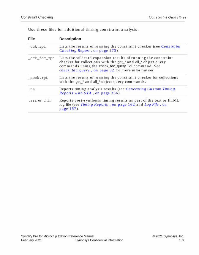
Constraint Checking Constraint Guidelines
Synplify Pro for Microchip Edition Reference Manual © 2021 Synopsys, Inc.February 2021 Synopsys Confidential Information 139
Use these files for additional timing constraint analysis:
File Description
_cck.rpt Lists the results of running the constraint checker (see Constraint Checking Report , on page 173).
_cck_fdc_rpt Lists the wildcard expansion results of running the constraint checker for collections with the get_* and all_* object query commands using the check_fdc_query Tcl command. See check_fdc_query , on page 32 for more information.
_scck.rpt Lists the results of running the constraint checker for collections with the get_* and all_* object query commands.
.ta Reports timing analysis results (see Generating Custom Timing Reports with STA , on page 366).
.srr or .htm Reports post-synthesis timing results as part of the text or HTML log file (see Timing Reports , on page 162 and Log File , on page 157).

LO
Constraint Guidelines Database Object Search
© 2021 Synopsys, Inc. Synplify Pro for Microchip Edition Reference Manual140 Synopsys Confidential Information February 2021
Database Object SearchTo apply constraints, you have to search the database to find the appropriate objects. Sometimes you might want to search for and apply the same constraint to multiple objects. The FPGA tool provides some Tcl commands to facilitate the search for database objects:
Commands Common Commands Description
Find Tcl Find, open_design... Lets you search for design objects to form collections that can apply constraints to the group. See Using Collections , on page 154 and find , on page 147.
Collections define_collection, c_union...
Create, copy, evaluate, traverse, and filter collections. See Using Collections , on page 154 and Collection Commands , on page 164 for more information.

Forward Annotation Constraint Guidelines
Synplify Pro for Microchip Edition Reference Manual © 2021 Synopsys, Inc.February 2021 Synopsys Confidential Information 141
Forward AnnotationThe tool can automatically generate vendor-specific constraint files for forward annotation to the place-and-route tools when you enable the Write Vendor Constraints switch (on the Implementation Results tab) or use the -write_apr_-constraint option of the set_option command.
For information about how forward annotation is handled for your target technology, refer to the appropriate vendor chapter of the FPGA Synthesis Reference Manual.
Auto ConstraintsAuto constraints are automatically generated by the synthesis tool, however, these do not replace regular timing constraints in the normal synthesis flow. Auto constraints are intended as a quick first pass to evaluate the kind of timing constraints you need to set in your design.
To enable this feature and automatically generate register-to-register constraints, use the Auto Constrain option. For details, see Using Auto Constraints, on page 376 in the User Guide.
Vendor File Extension
MicrochipPolarFire
_VM.SDC
MicrochipSmartFusion2
_SDC.SDC_VM.SDC
MicrochipAll devices except PolarFire and SmartFusion2
_SDC.SDC

LO
Constraint Guidelines Auto Constraints
© 2021 Synopsys, Inc. Synplify Pro for Microchip Edition Reference Manual142 Synopsys Confidential Information February 2021
Synplify Pro for Microchip Edition Reference Manual © 2021 Synopsys, Inc.February 2021 Synopsys Confidential Information 143
C H A P T E R 5
Input and Result Files
This chapter describes the input and output files used by the tool.
• Input Files, on page 144
• Libraries, on page 148
• Output Files, on page 152
• Log File, on page 157
• Timing Reports, on page 162
• Hierarchical Area Report, on page 172
• Constraint Checking Report, on page 173
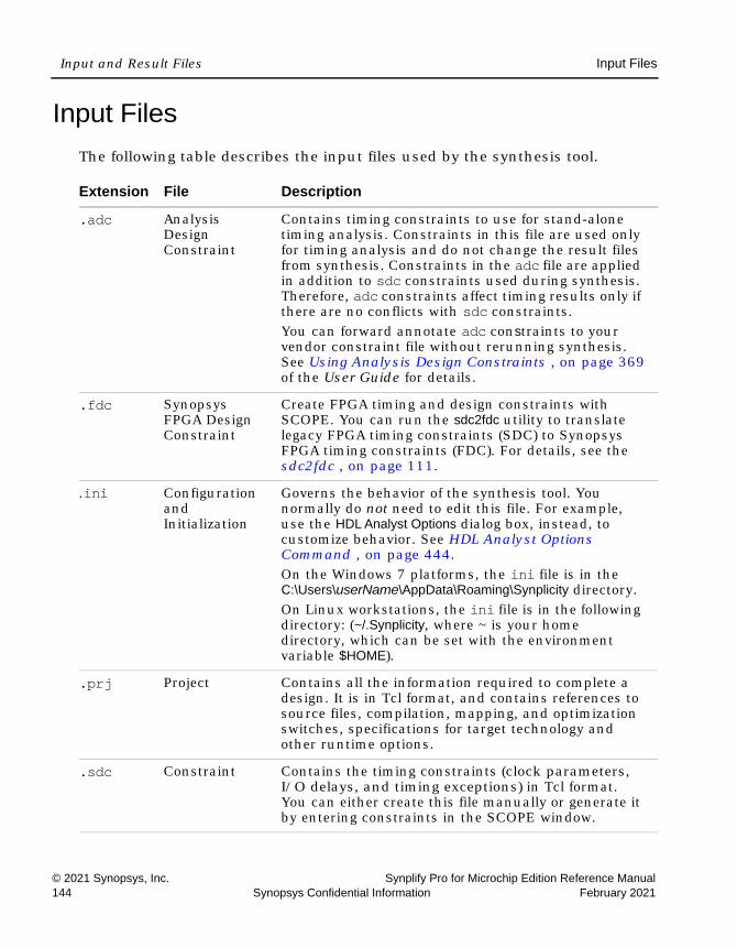
LO
Input and Result Files Input Files
© 2021 Synopsys, Inc. Synplify Pro for Microchip Edition Reference Manual144 Synopsys Confidential Information February 2021
Input FilesThe following table describes the input files used by the synthesis tool.
Extension File Description
.adc Analysis Design Constraint
Contains timing constraints to use for stand-alone timing analysis. Constraints in this file are used only for timing analysis and do not change the result files from synthesis. Constraints in the adc file are applied in addition to sdc constraints used during synthesis. Therefore, adc constraints affect timing results only if there are no conflicts with sdc constraints. You can forward annotate adc constraints to your vendor constraint file without rerunning synthesis. See Using Analysis Design Constraints , on page 369 of the User Guide for details.
.fdc Synopsys FPGA Design Constraint
Create FPGA timing and design constraints with SCOPE. You can run the sdc2fdc utility to translate legacy FPGA timing constraints (SDC) to Synopsys FPGA timing constraints (FDC). For details, see the sdc2fdc , on page 111.
.ini Configuration and Initialization
Governs the behavior of the synthesis tool. You normally do not need to edit this file. For example, use the HDL Analyst Options dialog box, instead, to customize behavior. See HDL Analyst Options Command , on page 444.On the Windows 7 platforms, the ini file is in the C:\Users\userName\AppData\Roaming\Synplicity directory. On Linux workstations, the ini file is in the following directory: (~/.Synplicity, where ~ is your home directory, which can be set with the environment variable $HOME).
.prj Project Contains all the information required to complete a design. It is in Tcl format, and contains references to source files, compilation, mapping, and optimization switches, specifications for target technology and other runtime options.
.sdc Constraint Contains the timing constraints (clock parameters, I/O delays, and timing exceptions) in Tcl format. You can either create this file manually or generate it by entering constraints in the SCOPE window.

Input Files Input and Result Files
Synplify Pro for Microchip Edition Reference Manual © 2021 Synopsys, Inc.February 2021 Synopsys Confidential Information 145
HDL Source FilesThe HDL source files for a project can be in either VHDL (.vhd), Verilog (.v), or SystemVerilog (.sv) format.
The Synopsys FPGA synthesis tool contains built-in macro libraries for vendor macros like gates, counters, flip-flops, and I/Os. If you use the built-in macro libraries, you can easily instantiate vendor macros directly into the VHDL designs, and forward-annotate them to the output netlist. Refer to the appropriate vendor support documentation for more information.
.sv Source files (Verilog)
Design source files in SystemVerilog format. The sv source file is added to the Verilog directory in the Project view. For more information about the Verilog and SystemVerilog languages, and the synthesis commands and attributes you can include, see Verilog , on page 146, Chapter 1, Verilog Language Support, and Chapter 2, SystemVerilog Language Support. For information about using VHDL and Verilog files together in a design, see Using Mixed Language Source Files , on page 48 of the User Guide.
.vhd Source files (VHDL)
Design source files in VHDL format. See VHDL , on page 146, Chapter 3, VHDL Language Support, and Chapter 4, VHDL 2008 Language Support for details. For information about using VHDL and Verilog files together in a design, see Using Mixed Language Source Files , on page 48 of the User Guide.
.v Source files (Verilog)
Design source files in Verilog format. For more information about the Verilog language, and the synthesis commands and attributes you can include, see Verilog , on page 146, Chapter 1, Verilog Language Support, and Chapter 2, SystemVerilog Language Support. For information about using VHDL and Verilog files together in a design, see Using Mixed Language Source Files , on page 48 of the User Guide.
Extension File Description

LO
Input and Result Files Input Files
© 2021 Synopsys, Inc. Synplify Pro for Microchip Edition Reference Manual146 Synopsys Confidential Information February 2021
VHDLThe Synopsys FPGA synthesis tool supports a synthesizable subset of VHDL93 (IEEE 1076), and the following IEEE library packages:
• numeric_bit
• numeric_std
• std_logic_1164
The synthesis tool also supports the following industry standards in the IEEE libraries:
• std_logic_arith
• std_logic_signed
• std_logic_unsigned
The Synopsys FPGA synthesis tool library contains an attributes package (installDirectory/lib/vhd/synattr.vhd) of built-in attributes and timing constraints that you can use with VHDL designs. The package includes declarations for timing constraints (including black-box timing constraints), vendor-specific attributes, and synthesis attributes. To access these built-in attributes, add the following two lines to the beginning of each of the VHDL design units that uses them:
library synplify;use synplify.attributes.all;
For more information about the VHDL language, and the synthesis commands and attributes you can include, see Chapter 3, VHDL Language Support and Chapter 4, VHDL 2008 Language Support.
VerilogThe Synopsys FPGA synthesis tool supports a synthesizable subset of Verilog 2001 and Verilog 95 (IEEE 1364) and SystemVerilog extensions. For more information about the Verilog language, and the synthesis commands and attributes you can include, see Chapter 1, Verilog Language Support and Chapter 2, SystemVerilog Language Support.

Input Files Input and Result Files
Synplify Pro for Microchip Edition Reference Manual © 2021 Synopsys, Inc.February 2021 Synopsys Confidential Information 147
The Synopsys FPGA synthesis tool contains built-in macro libraries for vendor macros like gates, counters, flip-flops, and I/Os. If you use the built-in macro libraries, you can instantiate vendor macros directly into Verilog designs and forward-annotate them to the output netlist. Refer to the User Guide for more information.
LO
Input and Result Files Libraries
© 2021 Synopsys, Inc. Synplify Pro for Microchip Edition Reference Manual148 Synopsys Confidential Information February 2021
LibrariesYou can instantiate components from a library, which can be either in Verilog or VHDL. For example, you might have technology-specific or custom IP components in a library, or you might have generic library components. The installDirectory/lib directory included with the software contains some compo-nent libraries you can use for instantiation.
There are several kinds of libraries you can use:
• Technology-specific libraries that contain I/O pad, macro, or other component descriptions. The lib directory lists these kinds of libraries under vendor sub-directories. The libraries are named for the technology family, and in some cases also include a version number for the version of the place-and-route tool with which they are intended to be used.
For information about using vendor-specific libraries to instantiate LPMs, PLLs, macros, I/O pads, and other components, refer to the appropriate sections in the Appendices of the Reference Manual.
• The open verification library is automatically included in the FPGA product installation. When using your own open verification library, follow the recommendation described in Open Verification Library (Verilog), on page 149.
• Technology-independent libraries that contain common components. You can have your own library or use the one Synopsys provides. This library is a Verilog library of common logic elements, much like the Synopsys® GTECH component library. See The Generic Technology Library, on page 149 for a description of this library.
• An ASIC Library Data Format file (.lib) is the technology library file that contains information about the functionality of each standard cell, its input capacitance, fanout, and timing information. For the synthesis flow to understand the instantiated or mapped ASIC primitives in the HDL, you would need to translate the functionality of the standard cell to equivalent synthesizable Verilog/VHDL definitions. To do this, you can use the lib2syn executable. For details, see ASIC Library Files, on page 150.

Libraries Input and Result Files
Synplify Pro for Microchip Edition Reference Manual © 2021 Synopsys, Inc.February 2021 Synopsys Confidential Information 149
Open Verification Library (Verilog)The open verification library is automatically included in the FPGA product installation. If you use your own version of the open verification library, then it is recommended that you disable loading the default synovl library to avoid any conflicts between the two libraries. To do this, set the -disable_synovl environment variable to 1. For example:
#in bashexport disable_synovl=1#in cshsetenv disable_synovl 1
When the default synovl library is disabled, the following message is gener-ated in the log file: @N::Open Verification Library which is part of tool installation, is being disabled by option "disable_synovl".
The Generic Technology LibraryThe synthesis software includes this Verilog library for generic components under the installDirectory/lib/generic_technology directory. Currently, the library is only available in Verilog format. The library consists of technology-indepen-dent common logic elements, which help the designer to develop technology-independent parts. The library models extract the functionality of the component, but not its implementation. During synthesis, the mappers implement these generic components in implementations that are appro-priate to the technology being used.
To use components from this directory, add the library to the project by doing either of the following:
• Add add_file -verilog "$LIB/generic_technology/gtech.v to your .prj file or type it in the Tcl window.
• In the tool window, click the Add file button, navigate to the installDirec-tory/lib/generic_technology directory and select the gtech.v file.
When you synthesize the design, the tool uses components from this library.
You cannot use the generic technology library together with other generic libraries, as this could result in a conflict. If you have your own GTECH library that you intend to use, do not use the generic technology library.

LO
Input and Result Files Libraries
© 2021 Synopsys, Inc. Synplify Pro for Microchip Edition Reference Manual150 Synopsys Confidential Information February 2021
ASIC Library FilesAn ASIC Library Data Format file (.lib) is the technology library file that contains information about the functionality of each standard cell, its input capacitance, fanout, and timing information.
For the synthesis flow to understand the instantiated or mapped ASIC primitives in the HDL, you would need to manually translate the functionality of the standard cell to equivalent synthesizable Verilog/VHDL definitions. This .lib file conversion is not automated in the synthesis flow. This means that the tool will not automatically translate .lib files into corresponding and equivalent synthesizable Verilog/VHDL definitions.
However, you can use the lib2syn executable to facilitate this conversion process. The lib2syn.exe executable generates equivalent synthesizable Verilog/VHDL definitions for the cells defined in the input .lib file. You can find this executable at these locations:
• Windows: installDirectory/bin/lib2syn.exe
• Linux: installDirectory/bin/lib2syn
The executable can be run as shown in these examples:
• For Verilog output: lib2syn.exe test.lib -ovm a.vm -logfile test_lib2syn.log
• For VHDL output: lib2syn.exe test.lib -ovhm a.vhm -logfile test_lib2syn.log
The tool supports the Synopsys GTECH library flow by default, so you do not need the .lib file equivalent synthesizable Verilog/VHDL definitions for a NETLIST mapped to a GTECH library.
Note that for the synthesis flow, the lib2syn executable does not translate cells with state table definitions.
The synthesis tools do not read Synopsys Liberty format (.syn) files directly. However, there are workarounds.
• If your design has instantiated ASIC cells, do the following:
– Get the Verilog functional files for the instantiated components.
– Add the functional files to your project as libraries.
• If you have an ASIC library in the Liberty (.lib) or .sel format, do the following:

Libraries Input and Result Files
Synplify Pro for Microchip Edition Reference Manual © 2021 Synopsys, Inc.February 2021 Synopsys Confidential Information 151
– Convert the ASIC library into a Verilog functional file with the lib2syn utility. The lib2syn command syntax is shown below:
installDirectory/bin/lib2syn.exe library.lib - ovm VerilogFunctionalFile
or
installDirectory/bin/lib2syn.exe library.sel -ovm VerilogFunctionalFile
– Add the functional file to your project as a library.

LO
Input and Result Files Output Files
© 2021 Synopsys, Inc. Synplify Pro for Microchip Edition Reference Manual152 Synopsys Confidential Information February 2021
Output FilesThe synthesis tool generates reports about the synthesis run and files that you can use for simulation or placement and routing. The following table describes the output files, categorizing them as either synthesis result and report files, or output files generated as input for other tools.
Extension File Description
.areasrr Hierarchical Area Report
Reports area-specific information such as sequential and combinational RAMs, DSPs, and Black Boxes on each module in the design. See Hierarchical Area Report , on page 172.
_cck.rpt Constraint Checker Report
Checks the syntax and applicability of the timing constraints in the .fdc file for your project and generates a report (projectName_cck.rpt). See Constraint Checking Report , on page 173 for more information.
_compiler.linkerlog Compiler log file for HDL source file linking
Provides details for why the VHDL and/or Verilog components in the source files were not properly linked. This file is located in the synwork directory for the implementation.
.fse FSM information file Design-dependent. Contains information about encoding types and transition states for all state machines in the design.
.info Design component files
Design-dependent. Contains detailed information about design components like state machines or ROMs.
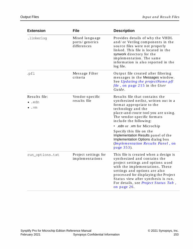
Output Files Input and Result Files
Synplify Pro for Microchip Edition Reference Manual © 2021 Synopsys, Inc.February 2021 Synopsys Confidential Information 153
.linkerlog Mixed language ports/generics differences
Provides details of why the VHDL and/or Verilog components in the source files were not properly linked. This file is located in the synwork directory for the implementation. The same information is also reported in the log file.
.pfl Message Filter criteria
Output file created after filtering messages in the Messages window. See Updating the projectName.pfl file , on page 215 in the User Guide.
Results file:• .edn• .vm
Vendor-specific results file
Results file that contains the synthesized netlist, written out in a format appropriate to the technology and the place-and-route tool you are using. The vendor-specific formats include the following:• .edn or .vm for MicrochipSpecify this file on the Implementation Results panel of the Implementation Options dialog box (Implementation Results Panel , on page 353).
run_options.txt Project settings for implementations
This file is created when a design is synthesized and contains the project settings and options used with the implementations. These settings and options are also processed for displaying the Project Status view after synthesis is run. For details, see Project Status Tab , on page 26.
Extension File Description
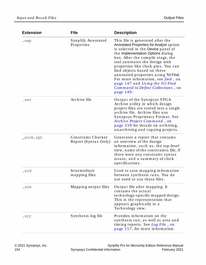
LO
Input and Result Files Output Files
© 2021 Synopsys, Inc. Synplify Pro for Microchip Edition Reference Manual154 Synopsys Confidential Information February 2021
.sap Synplify Annotated Properties
This file is generated after the Annotated Properties for Analyst option is selected in the Device panel of the Implementation Options dialog box. After the compile stage, the tool annotates the design with properties like clock pins. You can find objects based on these annotated properties using Tcl Find. For more information, see find , on page 147 and Using the Tcl Find Command to Define Collections , on page 149.
.sar Archive file Output of the Synopsys FPGA Archive utility in which design project files are stored into a single archive file. Archive files use Synopsys Proprietary Format. See Archive Project Command , on page 339 for details on archiving, unarchiving and copying projects.
_scck.rpt Constraint Checker Report (Syntax Only)
Generates a report that contains an overview of the design information, such as, the top-level view, name of the constraints file, if there were any constraint syntax issues, and a summary of clock specifications.
.srd Intermediate mapping files
Used to save mapping information between synthesis runs. You do not need to use these files.
.srm Mapping output files Output file after mapping. It contains the actual technology-specific mapped design. This is the representation that appears graphically in a Technology view.
.srr Synthesis log file Provides information on the synthesis run, as well as area and timing reports. See Log File , on page 157, for more information.
Extension File Description

Output Files Input and Result Files
Synplify Pro for Microchip Edition Reference Manual © 2021 Synopsys, Inc.February 2021 Synopsys Confidential Information 155
.srs Compiler output file Output file after the compiler stage of the synthesis process. It contains an HDL-level representation of a design. This is the representation that appears graphically in an RTL view.
synlog folder Intermediate technology mapping files
This folder contains intermediate netlists and log files after technology mapping has been run. Timestamp information is contained in these netlist files to manage jobs with up-to-date checks. For more information, see Using Up-to-date Checking for Job Management , on page 184.
synwork folder Intermediate pre-mapping files
This folder contains intermediate netlists and log files after pre-mapping has been run. Timestamp information is contained in these netlist files to manage jobs with up-to-date checks. For more information, see Using Up-to-date Checking for Job Management , on page 184.
.ta Customized Timing Report
Contains the custom timing information that you specify through Analysis->Timing Analyst. See Analysis Menu , on page 401, for more information.
_ta.srm Customized mapping output file
Creates a customized output netlist when you generate a custom timing report with HDL Analyst->Timing Analyst. It contains the representation that appears graphically in a Technology view. See Analysis Menu , on page 401 for more information.
Extension File Description

LO
Input and Result Files Output Files
© 2021 Synopsys, Inc. Synplify Pro for Microchip Edition Reference Manual156 Synopsys Confidential Information February 2021
.tap Timing Annotated Properties
This file is generated after the Annotated Properties for Analyst option is selected in the Device panel of the Implementation Options dialog box. After the compile stage, the tool annotates the design with timing properties and the information can be analyzed in the RTL view and Design Planner. You can also find objects based on these annotated properties using Tcl Find. For more information, see Using the Tcl Find Command to Define Collections , on page 149 in the User Guide.
.tlg Log file This log file contains a list of all the modules compiled in the design.
vendor constraint file Constraints file for forward annotation
Contains synthesis constraints to be forward-annotated to the place-and-route tool. The constraint file type varies with the vendor and the technology. Refer to the vendor chapters for specific information about the constraints you can forward-annotate. Check the Implementation Results dialog (Implementation Options) for supported files. See Implementation Results Panel , on page 353.
Extension File Description

Log File Input and Result Files
Synplify Pro for Microchip Edition Reference Manual © 2021 Synopsys, Inc.February 2021 Synopsys Confidential Information 157
Log FileThe log file report, located in the implementation directory, is written out in two file formats: text (projectName.srr) and HTML with an interactive table of contents (projectName.htm and projectName_srr.htm) where projectName is the name of your project. Select View Log File in HTML in the Options->Project View Options dialog box to enable viewing the log file in HTML. Select the View Log button in the Project view (Buttons and Options, on page 72) to see the log file report.
The log file is written each time you compile or synthesize (compile and map) the design. When you compile a design without mapping it, the log file contains only compiler information. As a precaution, a backup copy of the log file (.srr) is written to the backup sub-directory in the Implementation Results directory. Only one backup log file is updated for subsequent synthesis runs.
. vm
. vhm Mapped Verilog or VHDL netlist
Optional post-synthesis netlist file in Verilog (.vm) or VHDL (.vhm) format. This is a structural netlist of the synthesized design, and differs from the original HDL used as input for synthesis. Specify these files on the Implementation Results dialog box (Implementation Options). See Implementation Results Panel , on page 353.Typically, you use this netlist for gate-level simulation, to verify your synthesis results. Some designers prefer to simulate before and after synthesis, and also after place and route. This approach helps them to isolate the stage of the design process where a problem occurred. The Verilog and VHDL output files are for functional simulation only. When you input stimulus into a simulator for functional simulation, use a cycle time for the stimulus of 1000 time ticks.
Extension File Description

LO
Input and Result Files Log File
© 2021 Synopsys, Inc. Synplify Pro for Microchip Edition Reference Manual158 Synopsys Confidential Information February 2021
The log file contains detailed reports on the compiler, mapper, timing, and resource usage information for your design. Errors, notes, warnings, and messages appear in both the log file and on the Messages tab in the Tcl window.
For further details about different sections of the log file, see the following:
Compiler ReportThis report starts with the compiler version and date, and includes the following:
• Project information: the top-level module.
• Design information: HDL syntax and synthesis checks, black box instantiations, FSM extractions and inferred RAMs/ROMs.
For information about ... See ...
Compiled files, messages (warnings, errors, and notes), user options set for synthesis, state machine extraction information, including a list of reachable states.
Compiler Report , on page 158
Buffers added to clocks in certain supported technologies.
Clock Buffering Report , on page 159
Buffers added to nets. Net Buffering Report , on page 159
Compile point remapping. Compile Point Information , on page 160
Timing results. This section of the log file begins with “START TIMING REPORT” section. If you use the Timing Analyst to generate a custom timing report, its format is the same as the timing report in the log file, but the customized timing report is in a .ta file.
Timing Reports , on page 162
Resources used by synthesis mapping. Resource Usage Report , on page 160
Design changes made as a result of retiming. Retiming Report, on page 161
Design changes made as a result of gated clock conversion.
, on page 180

Log File Input and Result Files
Synplify Pro for Microchip Edition Reference Manual © 2021 Synopsys, Inc.February 2021 Synopsys Confidential Information 159
• Netlist filter information: constant propagation.
Premap ReportThis report begins with the pre-mapper version and date, and reports the following:
• File loading times and memory usage
• Clock summary - For details, see Clock Pre-map Reports, on page 165.
Mapper ReportThis report begins with the mapper version and date, and reports the following:
• Project information: the names of the constraint files, target technology, and attributes set in the design.
• Design information such as flattened instances, extraction of counters, FSM implementations, clock nets, buffered nets, replicated logic, HDL optimizations, and informational or warning messages.
Clock Buffering ReportThis section of the log file reports any clocks that were buffered. For example:
Clock Buffers:Inserting Clock buffer for port clock0,TNM=clock0
Net Buffering ReportNet buffering reports are generated for most all of the supported FPGAs and CPLDs. This information is written in the log file, and includes the following information:
• The nets that were buffered or had their source replicated
• The number of segments created for that net
• The total number of buffers added during buffering
• The number of registers and look-up tables (or other cells) added during replication

LO
Input and Result Files Log File
© 2021 Synopsys, Inc. Synplify Pro for Microchip Edition Reference Manual160 Synopsys Confidential Information February 2021
Example: Net Buffering ReportNet buffering Report:Badd_c[2] - loads: 24, segments 2, buffering sourceBadd_c[1] - loads: 32, segments 2, buffering sourceBadd_c[0] - loads: 48, segments 3, buffering sourceAadd_c[0] - loads: 32, segments 3, buffering sourceAdded 10 BuffersAdded 0 Registers via replicationAdded 0 LUTs via replication
Compile Point InformationThe Summary of Compile Points section of the log file (projectName.srr) lists each compile point, together with an indication of whether it was remapped, and, if so, why. Also, a timing report is generated for each compile point located in its respective results directories in the Implementation Directory. The compile point is the top-level design for this report file.
For more information on compile points and the compile-point synthesis flow, see Synthesizing Compile Points, on page 455 of the User Guide.
Timing SectionA default timing report is written to the log file (projectName.srr) in the “START OF TIMING REPORT” section. See Timing Reports, on page 162, for details.
For certain device technologies in the Synplify Pro tool, you can use the Timing Analyst to generate additional timing reports for point-to-point analysis (see Analysis Menu, on page 401). Their format is the same as the timing report.
Resource Usage ReportA resource usage report is added to the log file each time you compile or synthesize. The format of the report varies, depending on the architecture you are using. The report provides the following information:
• The total number of cells, and the number of combinational and sequen-tial cells in the design
• The number of clock buffers and I/O cells
• Details of how many of each type of cell in the design
Log File Input and Result Files
Synplify Pro for Microchip Edition Reference Manual © 2021 Synopsys, Inc.February 2021 Synopsys Confidential Information 161
See Checking Resource Usage, on page 201 in the User Guide for a brief procedure on using the report to check for overutilization.
Retiming ReportWhenever retiming is enabled, a retiming report is added to the log file (projectName.srr). It includes information about the design changes made as a result of retiming, such as the following:
• The number of flip-flops added, removed, or modified because of retiming. Flip-flops modified by retiming have a _ret suffix added to their names.
• Names of the flip-flops that were moved by retiming and no longer exist in the Technology view.
• Names of the flip-flops created as result of the retiming moves, that did not exist in the RTL view.
• Names of the flip-flops modified by retiming; for example, flip-flops that are in the RTL and Technology views, but have different fanouts because of retiming.
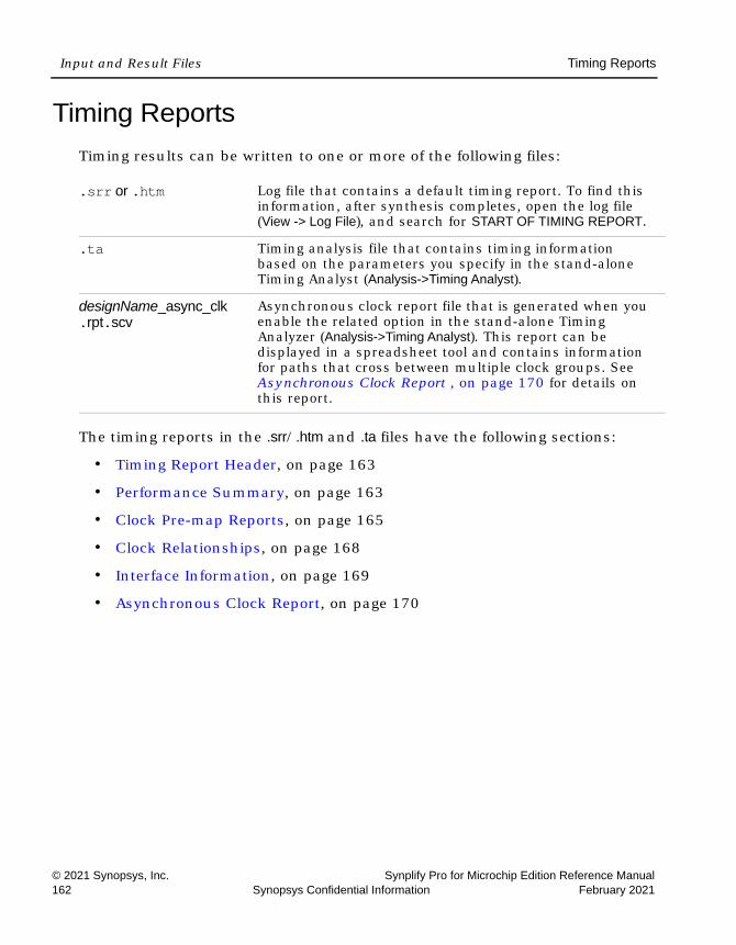
LO
Input and Result Files Timing Reports
© 2021 Synopsys, Inc. Synplify Pro for Microchip Edition Reference Manual162 Synopsys Confidential Information February 2021
Timing ReportsTiming results can be written to one or more of the following files:
The timing reports in the .srr/.htm and .ta files have the following sections:
• Timing Report Header, on page 163
• Performance Summary, on page 163
• Clock Pre-map Reports, on page 165
• Clock Relationships, on page 168
• Interface Information, on page 169
• Asynchronous Clock Report, on page 170
.srr or .htm Log file that contains a default timing report. To find this information, after synthesis completes, open the log file (View -> Log File), and search for START OF TIMING REPORT.
.ta Timing analysis file that contains timing information based on the parameters you specify in the stand-alone Timing Analyst (Analysis->Timing Analyst).
designName_async_clk.rpt.scv
Asynchronous clock report file that is generated when you enable the related option in the stand-alone Timing Analyzer (Analysis->Timing Analyst). This report can be displayed in a spreadsheet tool and contains information for paths that cross between multiple clock groups. See Asynchronous Clock Report , on page 170 for details on this report.

Timing Reports Input and Result Files
Synplify Pro for Microchip Edition Reference Manual © 2021 Synopsys, Inc.February 2021 Synopsys Confidential Information 163
Timing Report HeaderThe timing report header lists the date and time, the name of the top-level module, the number of paths requested for the timing report, and the constraint files used.
You can control the size of the timing report by choosing Project -> Implementa-tion Options, clicking the Timing Report tab of the panel, and specifying the number of start/end points and the number of critical paths to report. See Timing Report Panel, on page 355, for details.
Performance SummaryThe Performance Summary section of the timing report lists estimated and requested frequencies for the clocks, with the clocks sorted by negative slack. The timing report has a different section for detailed clock information.
The Performance Summary lists the following information for each clock in the design:
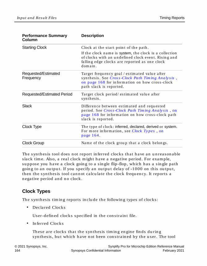
LO
Input and Result Files Timing Reports
© 2021 Synopsys, Inc. Synplify Pro for Microchip Edition Reference Manual164 Synopsys Confidential Information February 2021
The synthesis tool does not report inferred clocks that have an unreasonable slack time. Also, a real clock might have a negative period. For example, suppose you have a clock going to a single flip-flop, which has a single path going to an output. If you specify an output delay of -1000 on this output, then the synthesis tool cannot calculate the clock frequency. It reports a negative period and no clock.
Clock TypesThe synthesis timing reports include the following types of clocks:
• Declared Clocks
User-defined clocks specified in the constraint file.
• Inferred Clocks
These are clocks that the synthesis timing engine finds during synthesis, but which have not been constrained by the user. The tool
Performance Summary Column
Description
Starting Clock Clock at the start point of the path. If the clock name is system, the clock is a collection of clocks with an undefined clock event. Rising and falling edge clocks are reported as one clock domain.
Requested/Estimated Frequency
Target frequency goal /estimated value after synthesis. See Cross-Clock Path Timing Analysis , on page 168 for information on how cross-clock path slack is reported.
Requested/Estimated Period Target clock period/estimated value after synthesis.
Slack Difference between estimated and requested period. See Cross-Clock Path Timing Analysis , on page 168 for information on how cross-clock path slack is reported.
Clock Type The type of clock: inferred, declared, derived or system. For more information, see Clock Types , on page 164.
Clock Group Name of the clock group that a clock belongs.
Timing Reports Input and Result Files
Synplify Pro for Microchip Edition Reference Manual © 2021 Synopsys, Inc.February 2021 Synopsys Confidential Information 165
assigns the default global frequency specified for the project to these clocks.
• Derived Clocks
These are clocks that the synthesis tool identifies from a clock divider/multiplier such as DCM.
• System Clock
The system clock is the delay for the combinational path. Additionally, a system clock can be reported if there are sequential elements in the design for a clock network that cannot be traced back to a clock. Also, the system clock can occur for unconstrained I/O ports. You must investigate these conditions.
Paths to/from black boxes are timed by the system clock. Add the black-box timing constraints. See syn_black_box, on page 63 for the black box source code directives.
Clock Pre-map ReportsThe following clock reports are generated during pre-map.
• Clock Summary, on page 166
• Clock Load Summary, on page 166
• Clock Optimization Report, on page 167

LO
Input and Result Files Timing Reports
© 2021 Synopsys, Inc. Synplify Pro for Microchip Edition Reference Manual166 Synopsys Confidential Information February 2021
Clock SummaryHere is an example of the pre-map Clock Summary report.
Clock Load SummaryThe pre-map Clock Load Summary table contains the following:
• Clock name
• Number of clock loads
• Clock source pin
• Clock load on clock pin sequential example
• Clock load on non-clock pin sequential example
• Clock load on combinatorial example
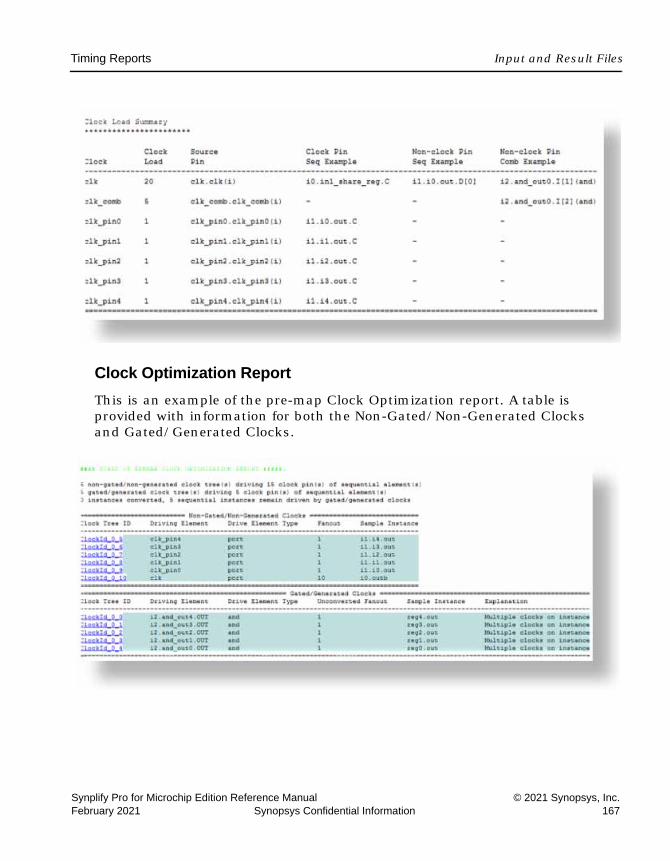
Timing Reports Input and Result Files
Synplify Pro for Microchip Edition Reference Manual © 2021 Synopsys, Inc.February 2021 Synopsys Confidential Information 167
Clock Optimization ReportThis is an example of the pre-map Clock Optimization report. A table is provided with information for both the Non-Gated/Non-Generated Clocks and Gated/Generated Clocks.
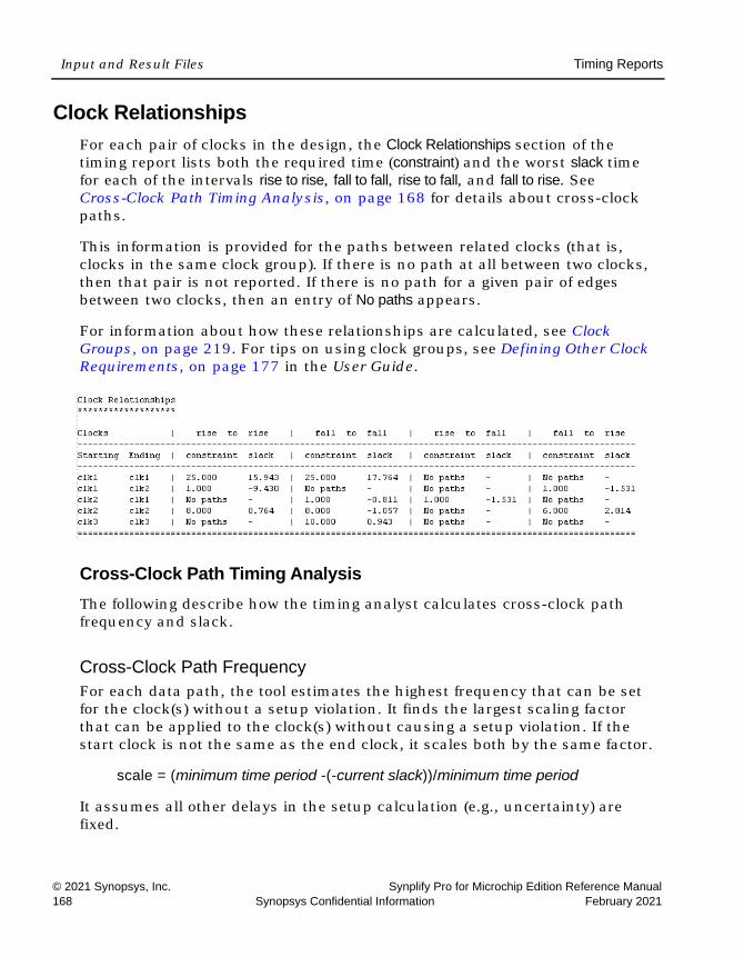
LO
Input and Result Files Timing Reports
© 2021 Synopsys, Inc. Synplify Pro for Microchip Edition Reference Manual168 Synopsys Confidential Information February 2021
Clock RelationshipsFor each pair of clocks in the design, the Clock Relationships section of the timing report lists both the required time (constraint) and the worst slack time for each of the intervals rise to rise, fall to fall, rise to fall, and fall to rise. See Cross-Clock Path Timing Analysis, on page 168 for details about cross-clock paths.
This information is provided for the paths between related clocks (that is, clocks in the same clock group). If there is no path at all between two clocks, then that pair is not reported. If there is no path for a given pair of edges between two clocks, then an entry of No paths appears.
For information about how these relationships are calculated, see Clock Groups, on page 219. For tips on using clock groups, see Defining Other Clock Requirements, on page 177 in the User Guide.
Cross-Clock Path Timing AnalysisThe following describe how the timing analyst calculates cross-clock path frequency and slack.
Cross-Clock Path FrequencyFor each data path, the tool estimates the highest frequency that can be set for the clock(s) without a setup violation. It finds the largest scaling factor that can be applied to the clock(s) without causing a setup violation. If the start clock is not the same as the end clock, it scales both by the same factor.
scale = (minimum time period -(-current slack))/minimum time period
It assumes all other delays in the setup calculation (e.g., uncertainty) are fixed.
Timing Reports Input and Result Files
Synplify Pro for Microchip Edition Reference Manual © 2021 Synopsys, Inc.February 2021 Synopsys Confidential Information 169
It applies relevant multicycle constraints to the setup calculation.
The estimated frequency for a clock is the minimum frequency over all paths that start or end on that clock, with the following exceptions:
• The tool does not consider paths between the system clock and another clock to estimate frequency.
• It considers paths with a path delay constraint to be asynchronous, and does not use them to estimate frequency.
• It considers paths between clocks in different domains to be asynchro-nous, and does not use them to estimate frequency.
Slack for Cross-Clock Paths The slack reported for a cross-clock path is the worst slack for any path that starts on that clock. Note that this differs from the estimated frequency calcu-lation, which is based on the worst slack for any path starting or ending on that clock.
Interface InformationThe interface section of the timing report contains information on arrival times, required times, and slack for the top-level ports. It is divided into two subsections, one each for Input Ports and Output Ports. Bidirectional ports are listed under both. For each port, the interface report contains the following information.
Port parameter Description
Port Name Port name.
Starting Reference Clock The reference clock.
User Constraint The input/output delay. If a port has multiple delay records, the report contains the values for the record with the worst slack. The reference clock corresponds to the worst slack delay record.
LO
Input and Result Files Timing Reports
© 2021 Synopsys, Inc. Synplify Pro for Microchip Edition Reference Manual170 Synopsys Confidential Information February 2021
Asynchronous Clock ReportYou can generate a report for paths that cross between clock groups using the stand-alone Timing Analyst (Analysis->Timing Analyst, Generate Asynchronous Clock Report check box). Generally, paths in different clock groups are automatically handled as false paths. This option provides a file that contains information on each of the paths and can be viewed in a spreadsheet tool. To display the CSV-format report:
1. Locate the file in your results directory projectName_async_clk.rpt.csv.2. Open the file in your spreadsheet tool.
Arrival Time Input ports: define_input_delay, or default value of 0.Output ports: path delay (including clock-to-out delay of source register).For purely combinational paths, the propagation delay is calculated from the driving input port.
Required Time Input ports: clock period - (path delay + setup time of receiving register + define_reg_input_delay value).Output ports: clock period - define_output_delay. Default value of define_output_delay is 0.
Slack Required Time - Arrival Time
Column Description
Index Path number.
Path Delay Delay value as reported in standard timing (ta) file.
Logic Levels Number of logic levels in the path (such as LUTs, cells, and so on) that are between the start and end points.
Types Cell types, such as LUT, logic cell, and so on.
Route Delay As reported for each path in ta
Source Clock Start clock.
Destination Clock End clock.
Port parameter Description
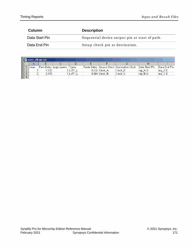
Timing Reports Input and Result Files
Synplify Pro for Microchip Edition Reference Manual © 2021 Synopsys, Inc.February 2021 Synopsys Confidential Information 171
Data Start Pin Sequential device output pin at start of path.
Data End Pin Setup check pin at destination.
Column Description

LO
Input and Result Files Hierarchical Area Report
© 2021 Synopsys, Inc. Synplify Pro for Microchip Edition Reference Manual172 Synopsys Confidential Information February 2021
Hierarchical Area ReportAn area report is created during synthesis which contains the percentage utilization for elements in the design, as well as, total sequential utilization for elements of specific modules. For instance, elements can include sequen-tial, combinational, or memory elements. They can also include the following types of technology-specific elements for ROMs, I/O pads, or DSPs.
This report generates technology-specific area information that is reflected in the output depending upon the specified device. The report is written to the projectName.areasrr file. You can view the file with the log viewer or any text editor.
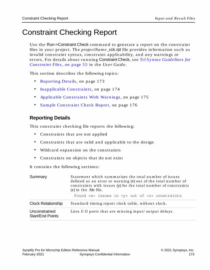
Constraint Checking Report Input and Result Files
Synplify Pro for Microchip Edition Reference Manual © 2021 Synopsys, Inc.February 2021 Synopsys Confidential Information 173
Constraint Checking ReportUse the Run->Constraint Check command to generate a report on the constraint files in your project. The projectName_cck.rpt file provides information such as invalid constraint syntax, constraint applicability, and any warnings or errors. For details about running Constraint Check, see Tcl Syntax Guidelines for Constraint Files, on page 55 in the User Guide.
This section describes the following topics:
• Reporting Details, on page 173
• Inapplicable Constraints, on page 174
• Applicable Constraints With Warnings, on page 175
• Sample Constraint Check Report, on page 176
Reporting DetailsThis constraint checking file reports the following:
• Constraints that are not applied
• Constraints that are valid and applicable to the design
• Wildcard expansion on the constraints
• Constraints on objects that do not exist
It contains the following sections:
Summary Statement which summarizes the total number of issues defined as an error or warning (x) out of the total number of constraints with issues (y) for the total number of constraints (z) in the .fdc file. Found <x> issues in <y> out of <z> constraints
Clock Relationship Standard timing report clock table, without slack.
Unconstrained Start/End Points
Lists I/O ports that are missing input/output delays.

LO
Input and Result Files Constraint Checking Report
© 2021 Synopsys, Inc. Synplify Pro for Microchip Edition Reference Manual174 Synopsys Confidential Information February 2021
Inapplicable ConstraintsRefer to the following table for constraints that were not applied because objects do not exist or the object type check was not valid:
Unapplied constraints
Constraints that cannot be applied because objects do not exist or the object type check is not valid. See Inapplicable Constraints , on page 174 for more information.
Applicable constraints with issues
Constraints will be applied either fully or partially, but there might be issues that generate warnings which should be investigated, such as some objects/collections not existing. Also, whenever at least one object in a list of objects is not specified with a valid object type a warning is displayed. See Applicable Constraints With Warnings , on page 175 for more information.
Constraints with matching wildcard expressions
Lists constraints or collections using wildcard expressions up to the first 1000, respectively.
For these constraints ... Objects must be ...
Attributes Valid definitions
create_clock • Ports• Nets• Pins• Registers• Instantiated buffers
create_generated_clock Clocks
define_compile_point • Region• View
define_current_design v:view

Constraint Checking Report Input and Result Files
Synplify Pro for Microchip Edition Reference Manual © 2021 Synopsys, Inc.February 2021 Synopsys Confidential Information 175
Applicable Constraints With WarningsThe following table lists reasons for warnings in the report file:
set_false_path set_multicycle_pathset_max_delay
For -to or -from objects:• i:sequential instances• p:ports• i:black boxesFor -through objects• n:nets• t:hierarchical ports• t:pins
set_multicycle_path Specified as a positive integer
set_input_delay • Input ports• bidir ports
set_output_delay • Output ports• Bidir ports
set_reg_input_delayset_reg_output_delay
Sequential instances
For these constraints ... Objects must be ...
create_clock • Ports• Nets• Pins• Registers• Instantiated buffers
set_clock_uncertainty A single object. Multiple objects are not supported.
define_compile_point A single object. Multiple objects are not supported.
define_current_design v:view
For these constraints ... Objects must be ...
LO
Input and Result Files Constraint Checking Report
© 2021 Synopsys, Inc. Synplify Pro for Microchip Edition Reference Manual176 Synopsys Confidential Information February 2021
Sample Constraint Check ReportThe following is a sample report generated by constraint checking:
# Synopsys Constraint Checker, version maprc, Build 1138R, built Jun 7 2016# Copyright (C) 1994-2016, Synopsys, Inc.
# Written on Fri Jun 7 09:42:22 2016##### DESIGN INFO #######################################################
Top View: "decode_top"Constraint File(s): "C:\timing_88\FPGA_decode_top.sdc"##### SUMMARY ############################################################
Found 3 issues in 2 out of 27 constraints
set_false_path set_multicycle_pathset_path_delay
For -to or -from objects:• i:sequential instances• p:ports• i:black boxesFor -through objects:• n:nets• t:hierarchical ports• t:pins
set_input_delay A single object. Multiple objects are not supported.
set_output_delay A single object. Multiple objects are not supported.
set_reg_input_delayset_reg_output_delay
A single object. Multiple objects are not supported.
For these constraints ... Objects must be ...

Constraint Checking Report Input and Result Files
Synplify Pro for Microchip Edition Reference Manual © 2021 Synopsys, Inc.February 2021 Synopsys Confidential Information 177
##### DETAILS ############################################################
Clock Relationships*******************
Starting Ending | rise to rise | fall to fall | rise to fall | fall to rise------------------------------------------------------------------------------------clk2x clk2x | 24.000 | 24.000 | 12.000 | 12.000 ------------------------------------------------------------------------------------clk2x clk | 24.000 | No paths | No paths | 12.000 clk clk2x | 24.000 | No paths | 12.000 | No paths clk clk | 48.000 | No paths | No paths | No paths ====================================================================================Note: 'No paths' indicates there are no paths in the design for that pair of clock edges.'Diff grp' indicates that paths exist but the starting clock and ending clock are in different clock groups
Unconstrained Start/End Points******************************p:test_mode
Inapplicable constraints************************
set_false_path -from p:next_synd -through i:core.tab1.ram_loader@E:|object "i:core.tab1.ram_loader" does not exist@E:|object "i:core.tab1.ram_loader" is incorrect type; "-through" objects must be of type net (n:), or pin (t:)
Applicable constraints with issues**********************************
set_false_path -from {core.decoder.root_mult*.root_prod_pre[*]} -to {i:core.decoder.omega_inst.omega_tmp_d_lch[7:0]}@W:|object "core.decoder.root_mult*.root_prod_pre[*]" is missing qualifier which may result in undesired results; "-from" objects must be of type clock (c:), inst (i:), port (p:), or pin (t:)
Constraints with matching wildcard expressions**********************************************
set_false_path -from {core.decoder.root_mult*.root_prod_pre[*]} -to {i:core.decoder.omega_inst.omega_tmp_d_lch[7:0]}@N:|expression "core.decoder.root_mult*.root_prod_pre[*]" applies to objects:core.decoder.root_mult1.root_prod_pre[14:0]core.decoder.root_mult.root_prod_pre[14:0]

LO
Input and Result Files Constraint Checking Report
© 2021 Synopsys, Inc. Synplify Pro for Microchip Edition Reference Manual178 Synopsys Confidential Information February 2021
set_false_path -from {i:core.decoder.*.root_prod_pre[*]} -to {i:core.decoder.t_*_[*]}@N:|expression "core.decoder.*.root_prod_pre[*]" applies to objects:core.decoder.root_mult1.root_prod_pre[14:0]core.decoder.root_mult.root_prod_pre[14:0]@N:|expression "core.decoder.t_*_[*]" applies to objects:core.decoder.t_20_[7:0]core.decoder.t_19_[7:0]core.decoder.t_18_[7:0]core.decoder.t_17_[7:0]core.decoder.t_16_[7:0]core.decoder.t_15_[7:0]core.decoder.t_14_[7:0]core.decoder.t_13_[7:0]core.decoder.t_12_[7:0]core.decoder.t_11_[7:0]core.decoder.t_10_[7:0]core.decoder.t_9_[7:0]core.decoder.t_8_[7:0]core.decoder.t_7_[7:0]core.decoder.t_6_[7:0]core.decoder.t_5_[7:0]core.decoder.t_4_[7:0]core.decoder.t_3_[7:0]core.decoder.t_2_[7:0]core.decoder.t_1_[7:0]core.decoder.t_0_[7:0]
set_false_path -from {i:core.decoder.root_mult*.root_prod_pre[*]} -to {i:core.decoder.err[7:0]}N:|expression "core.decoder.root_mult*.root_prod_pre[*]" applies to objects:core.decoder.root_mult1.root_prod_pre[14:0]core.decoder.root_mult.root_prod_pre[14:0]
set_false_path -from {i:core.decoder.root_mult*.root_prod_pre[*]} -to {i:core.decoder.omega_inst.deg_omega[4:0]}@N:|expression "core.decoder.root_mult*.root_prod_pre[*]" applies to objects:core.decoder.root_mult1.root_prod_pre[14:0]core.decoder.root_mult.root_prod_pre[14:0]
set_false_path -from {i:core.decoder.root_mult*.root_prod_pre[*]} -to {i:core.decoder.omega_inst.omega_tmp[0:7]}@N:|expression "core.decoder.root_mult*.root_prod_pre[*]" applies to objects:core.decoder.root_mult1.root_prod_pre[14:0]core.decoder.root_mult.root_prod_pre[14:0]
set_false_path -from {i:core.decoder.root_mult*.root_prod_pre[*]} -to {i:core.decoder.root[7:0]}@N:|expression "core.decoder.root_mult*.root_prod_pre[*]" applies to objects:core.decoder.root_mult1.root_prod_pre[14:0]core.decoder.root_mult.root_prod_pre[14:0]

Constraint Checking Report Input and Result Files
Synplify Pro for Microchip Edition Reference Manual © 2021 Synopsys, Inc.February 2021 Synopsys Confidential Information 179
set_false_path -from {i:core.decoder.root_mult*.root_prod_pre[*]} -to {i:core.decoder.root_inst.count[3:0]}N:|expression "core.decoder.root_mult*.root_prod_pre[*]" applies to objects:core.decoder.root_mult1.root_prod_pre[14:0]core.decoder.root_mult.root_prod_pre[14:0]
set_false_path -from {i:core.decoder.root_mult*.root_prod_pre[*]} -to {i:core.decoder.root_inst.q_reg[7:0]}@N:|expression "core.decoder.root_mult*.root_prod_pre[*]" applies to objects:core.decoder.root_mult1.root_prod_pre[14:0]core.decoder.root_mult.root_prod_pre[14:0]
set_false_path -from {i:core.decoder.root_mult*.root_prod_pre[*]} -to {i:core.decoder.root_inst.q_reg_d_lch[7:0]}@N:|expression "core.decoder.root_mult*.root_prod_pre[*]" applies to objects:core.decoder.root_mult1.root_prod_pre[14:0]core.decoder.root_mult.root_prod_pre[14:0]
set_false_path -from {i:core.decoder.root_mult.root_prod_pre[*]} -to {i:core.decoder.error_inst.den[7:0]}@N:|expression "core.decoder.root_mult.root_prod_pre[*]" applies to objects:core.decoder.root_mult.root_prod_pre[14:0]
set_false_path -from {i:core.decoder.root_mult1.root_prod_pre[*]} -to {i:core.decoder.error_inst.num1[7:0]}@N:|expression "core.decoder.root_mult1.root_prod_pre[*]" applies to objects:core.decoder.root_mult1.root_prod_pre[14:0]
set_false_path -from {i:core.decoder.synd_reg_*_[7:0]} -to {i:core.decoder.b_*_[7:0]}@N:|expression "core.decoder.synd_reg_*_[7:0]" applies to objects:core.decoder.un1_synd_reg_0_[7:0]core.decoder.synd_reg_20_[7:0]core.decoder.synd_reg_19_[7:0]core.decoder.synd_reg_18_[7:0]core.decoder.synd_reg_17_[7:0]core.decoder.synd_reg_16_[7:0]core.decoder.synd_reg_15_[7:0]core.decoder.synd_reg_14_[7:0]core.decoder.synd_reg_13_[7:0]core.decoder.synd_reg_12_[7:0]core.decoder.synd_reg_11_[7:0]core.decoder.synd_reg_10_[7:0]core.decoder.synd_reg_9_[7:0]core.decoder.synd_reg_8_[7:0]core.decoder.synd_reg_7_[7:0]core.decoder.synd_reg_6_[7:0]core.decoder.synd_reg_5_[7:0]core.decoder.synd_reg_4_[7:0]core.decoder.synd_reg_3_[7:0]core.decoder.synd_reg_2_[7:0]core.decoder.synd_reg_1_[7:0]

LO
Input and Result Files Constraint Checking Report
© 2021 Synopsys, Inc. Synplify Pro for Microchip Edition Reference Manual180 Synopsys Confidential Information February 2021
@N:|expression "core.decoder.b_*_[7:0]" applies to objects:core.decoder.un1_b_0_[7:0]core.decoder.b_calc.un1_lambda_0_[7:0]core.decoder.b_20_[7:0]core.decoder.b_19_[7:0]core.decoder.b_18_[7:0]core.decoder.b_17_[7:0]core.decoder.b_16_[7:0]core.decoder.b_15_[7:0]core.decoder.b_14_[7:0]core.decoder.b_13_[7:0]core.decoder.b_12_[7:0]core.decoder.b_11_[7:0]core.decoder.b_10_[7:0]core.decoder.b_9_[7:0]core.decoder.b_8_[7:0]core.decoder.b_7_[7:0]core.decoder.b_6_[7:0]core.decoder.b_5_[7:0]core.decoder.b_4_[7:0]core.decoder.b_3_[7:0]core.decoder.b_2_[7:0]core.decoder.b_1_[7:0]core.decoder.b_0_[7:0
Library Report**************
# End of Constraint Checker Report

Synplify Pro for Microchip Edition Reference Manual © 2021 Synopsys, Inc.February 2021 Synopsys Confidential Information 181
C H A P T E R 6
RAM and ROM Inference
This chapter provides guidelines and Verilog or VHDL examples for coding RAMs for synthesis. It covers the following topics:
• Guidelines and Support for RAM Inference, on page 182
• Automatic RAM Inference, on page 183
• Block RAM Inference, on page 187
• Initial Values for RAMs, on page 229
• RAM Instantiation with SYNCORE, on page 242
• ROM Inference, on page 243

LO
RAM and ROM Inference Guidelines and Support for RAM Inference
© 2021 Synopsys, Inc. Synplify Pro for Microchip Edition Reference Manual182 Synopsys Confidential Information February 2021
Guidelines and Support for RAM InferenceThere are two methods to handle RAMs: instantiation and inference. Many FPGA families provide technology-specific RAMs that you can instantiate in your HDL source code. The software supports instantiation, but you can also set up your source code so that it infers the RAMs. The following table sums up the pros and cons of the two approaches.
You must structure your source code correctly for the type of RAM you want to infer. The following table lists the supported technology-specific RAMs that can be generated by the synthesis tool.
Inference in Synthesis Instantiation
AdvantagesPortable coding styleAutomatic timing-driven synthesisNo additional tool dependencies
AdvantagesMost efficient use of the RAM primitives of a specific technologySupports all kinds of RAMs
LimitationsGlue logic to implement the RAM might result in a sub-optimal implementation Can only infer synchronous RAMsNo support for address wrappingPin name limitations means some pins are always active or inactive
LimitationsSource code is not portable because it is technology-dependent Limited or no access to timing and area data if the RAM is a black box Inter-tool access issues, if the RAM is a black box created with another tool
RAM Type Microchip
Single Port x
Dual Port x
True Dual Port
x

Automatic RAM Inference RAM and ROM Inference
Synplify Pro for Microchip Edition Reference Manual © 2021 Synopsys, Inc.February 2021 Synopsys Confidential Information 183
Automatic RAM InferenceInstead of instantiating synchronous RAMs, you can let the synthesis tools automatically infer them directly from the HDL source code and map them to the appropriate technology-specific RAM resources on the FPGA. This approach lets you maintain portability.
Here are some of the advantages offered by the inference approach:
• The tool automatically infers the RAM from the HDL code, which is technology-independent. This means that the design is portable from one technology to another without rework.
• RAM inference is the best method for prototyping.
• The tool automatically adds the extra glue logic needed to ensure that the logic is correct.
• The software automatically runs timing-driven synthesis for inferred RAMs.
Block RAMThe synthesis software can implement the block RAM it infers using different types of block RAM and different block RAM modes.
Types of Block RAMThe synthesis software can infer different kinds of block RAM, according to how the code is set up. For details about block RAM inference, see Block RAM Inference, on page 187 and RAM Attributes, on page 184. For inference examples, and see Block RAM Examples, on page 193.
The synthesis tool can infer the following kinds of block RAM:
• Single-port RAM
• Dual-port RAM
Based on how the read and write ports are used, dual-port RAM can be further classified as follows:
– Simple dual-port
– Dual-port
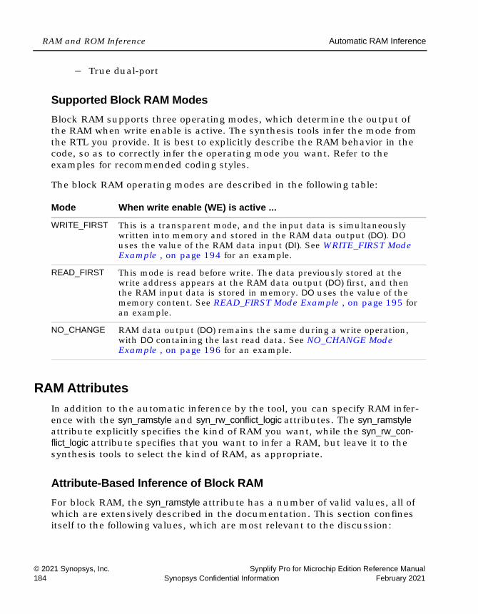
LO
RAM and ROM Inference Automatic RAM Inference
© 2021 Synopsys, Inc. Synplify Pro for Microchip Edition Reference Manual184 Synopsys Confidential Information February 2021
– True dual-port
Supported Block RAM ModesBlock RAM supports three operating modes, which determine the output of the RAM when write enable is active. The synthesis tools infer the mode from the RTL you provide. It is best to explicitly describe the RAM behavior in the code, so as to correctly infer the operating mode you want. Refer to the examples for recommended coding styles.
The block RAM operating modes are described in the following table:
RAM AttributesIn addition to the automatic inference by the tool, you can specify RAM infer-ence with the syn_ramstyle and syn_rw_conflict_logic attributes. The syn_ramstyle attribute explicitly specifies the kind of RAM you want, while the syn_rw_con-flict_logic attribute specifies that you want to infer a RAM, but leave it to the synthesis tools to select the kind of RAM, as appropriate.
Attribute-Based Inference of Block RAM For block RAM, the syn_ramstyle attribute has a number of valid values, all of which are extensively described in the documentation. This section confines itself to the following values, which are most relevant to the discussion:
Mode When write enable (WE) is active ...
WRITE_FIRST This is a transparent mode, and the input data is simultaneously written into memory and stored in the RAM data output (DO). DO uses the value of the RAM data input (DI). See WRITE_FIRST Mode Example , on page 194 for an example.
READ_FIRST This mode is read before write. The data previously stored at the write address appears at the RAM data output (DO) first, and then the RAM input data is stored in memory. DO uses the value of the memory content. See READ_FIRST Mode Example , on page 195 for an example.
NO_CHANGE RAM data output (DO) remains the same during a write operation, with DO containing the last read data. See NO_CHANGE Mode Example , on page 196 for an example.

Automatic RAM Inference RAM and ROM Inference
Synplify Pro for Microchip Edition Reference Manual © 2021 Synopsys, Inc.February 2021 Synopsys Confidential Information 185
If you specify the syn_rw_conflict_logic attribute, the synthesis tools can infer block RAM, depending on the design. If the tool does infer block RAM, it does not insert bypass logic around the block RAM to account for read-write conflicts and prevent simulation mismatches. In this way its functionality is the same as syn_ramstyle with no_rw_check, which does not insert bypass logic either.
Specifying the AttributesYou set the attribute in the HDL source code, through the SCOPE interface or in an FPGA constraint file.
HDL Source CodeSet the attribute on the Verilog register or VHDL signal that holds the output values of the RAM. The following syntax shows how to specify the attribute in Verilog and VHDL code:
SCOPEFor the syn_ramstyle attribute, set the attribute on the RAM register memory signal, mem, as shown below. For the syn_rw_conflict_logic attribute, set it on the instance or set it globally. The attributes are written out to a constraints file using the syntax described in the next section.
syn_ramstyle Value Description
block_ram Enforces the inference and implementation of a technology-specific RAM.
registers Prevents inference of a RAM, and maps the RAM to flip-flops and logic.
no_rw_check Does not create overhead logic to account for read-write conflicts.
Verilog reg [7:0] ram_dout [127:0] /*synthesis syn_ramstyle = "block_ram"*/;reg [d_width-1:0] mem [mem_depth-1:0] /*synthesis syn_rw_conflict_logic = 0*/;
VHDL attribute syn_ramstyle of ram_dout : signal is "block_ram";

LO
RAM and ROM Inference Automatic RAM Inference
© 2021 Synopsys, Inc. Synplify Pro for Microchip Edition Reference Manual186 Synopsys Confidential Information February 2021
Constraints FileIn the fdc Tcl constraints file written out from the SCOPE interface, the syn_ramstyle attribute is attached to the register mem signal of the RAM, and the syn_rw_conflict_logic attribute is attached to the view, as shown below:
define_attribute {i:mem[7:0]} {syn_ramstyle} {block_ram}define_attribute {v:mem[0:7]} syn_rw_conflict_logic {0}
For the syn_rw_conflict_logic attribute, you can also specify it globally, as well as on individual modules and instances:
define_global_attribute syn_rw_conflict_logic {0}

Block RAM Inference RAM and ROM Inference
Synplify Pro for Microchip Edition Reference Manual © 2021 Synopsys, Inc.February 2021 Synopsys Confidential Information 187
Block RAM InferenceBased on the design and how you code it, the tool can infer the following kinds of block RAM: single-port, simple dual-port, dual-port, and true dual-port. The details about RAM inference and setup guidelines are described here:
• Setting up the RTL and Inferring Block RAM, on page 187
• Simple Dual-Port Block RAM Inference, on page 189
• Dual-Port RAM Inference, on page 191
• True Dual-Port RAM Inference, on page 191
• True Dual-Port Byte-Enabled RAM Inference, on page 192
Setting up the RTL and Inferring Block RAMTo ensure that the tool infers the kind of block RAM you want, do the following:
1. Set up the RAM HDL code in accordance with the following guidelines:
– The RAM must be synchronous. It must not have any asynchronous control signals connected. The synthesis tools do not infer asynchronous block RAM.
– You must register either the read address or the output.
– The RAMs must not be too small, as the tool does not infer block RAM for small-sized RAMs. The size threshold varies with the target technology.

LO
RAM and ROM Inference Block RAM Inference
© 2021 Synopsys, Inc. Synplify Pro for Microchip Edition Reference Manual188 Synopsys Confidential Information February 2021
2. Set up the clocks and read and write ports to infer the kind of RAM you want. The following table summarizes how to set up the RAM in the RTL:
For illustrative code examples, see the single-port and dual-port examples listed in Block RAM Examples, on page 193.
3. If needed, guide automatic inference with the syn_ramstyle attribute:
– To force the inference of block RAM, specify syn_ramstyle=blockram.
– To prevent a block RAM from being inferred or if your resources are limited, use syn_ramstyle=registers.
– If you know your design does not read and write to the same address simultaneously, specify syn_ramstyle=no_rw_check to ensure that the synthesis tool does not unnecessarily create bypass logic for resolving conflicts.
4. Synthesize the design.
The tool first compiles the design and infers the RAMs, which it represents as abstract technology-independent primitives like RAM1 and RAM2. You can view these RAMs in the RTL view, which is a graphic, technology-independent representation of your design after compilation:
RAM Clock Read Ports Write Ports
Single-port Single clock One; same as write One; same as read
Simple dual-port
Single or dual clock
One dedicated read One dedicated write
Dual-port Single or dual clock
Two independent reads
One dedicated write
True dual-port Single or dual clock
Two independent reads
Two independent writes
See Dual-Port RAM Inference , on page 191 and True Dual-Port RAM Inference , on page 191 for additional information.
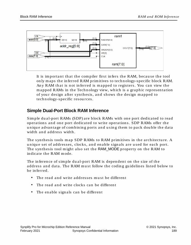
Block RAM Inference RAM and ROM Inference
Synplify Pro for Microchip Edition Reference Manual © 2021 Synopsys, Inc.February 2021 Synopsys Confidential Information 189
It is important that the compiler first infers the RAM, because the tool only maps the inferred RAM primitives to technology-specific block RAM. Any RAM that is not inferred is mapped to registers. You can view the mapped RAMs in the Technology view, which is a graphic representation of your design after synthesis, and shows the design mapped to technology-specific resources.
Simple Dual-Port Block RAM InferenceSimple dual-port RAMs (SDP) are block RAMs with one port dedicated to read operations and one port dedicated to write operations. SDP RAMs offer the unique advantage of combining ports and using them to pack double the data width and address width.
The synthesis tools map SDP RAMs to RAM primitives in the architecture. A unique set of addresses, clocks, and enable signals are used for each port. The synthesis tool might also set the RAM_MODE property on the RAM to indicate the RAM mode.
The inference of simple dual-port RAM is dependent on the size of the address and data. The RAM must follow the coding guidelines listed below to be inferred.
• The read and write addresses must be different
• The read and write clocks can be different
• The enable signals can be different
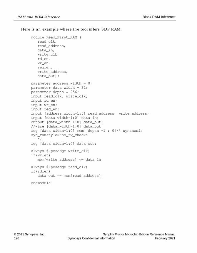
LO
RAM and ROM Inference Block RAM Inference
© 2021 Synopsys, Inc. Synplify Pro for Microchip Edition Reference Manual190 Synopsys Confidential Information February 2021
Here is an example where the tool infers SDP RAM:
module Read_First_RAM (read_clk,read_address,data_in,write_clk,rd_en,wr_en,reg_en,write_address,data_out);
parameter address_width = 8;parameter data_width = 32;parameter depth = 256;input read_clk, write_clk;input rd_en;input wr_en;input reg_en;input [address_width-1:0] read_address, write_address;input [data_width-1:0] data_in;output [data_width-1:0] data_out;//wire [data_width-1:0] data_out;reg [data_width-1:0] mem [depth -1 : 0]/* synthesis syn_ramstyle="no_rw_check"
*/;reg [data_width-1:0] data_out;always @(posedge write_clk)if(wr_en)
mem[write_address] <= data_in;always @(posedge read_clk)if(rd_en)
data_out <= mem[read_address];endmodule
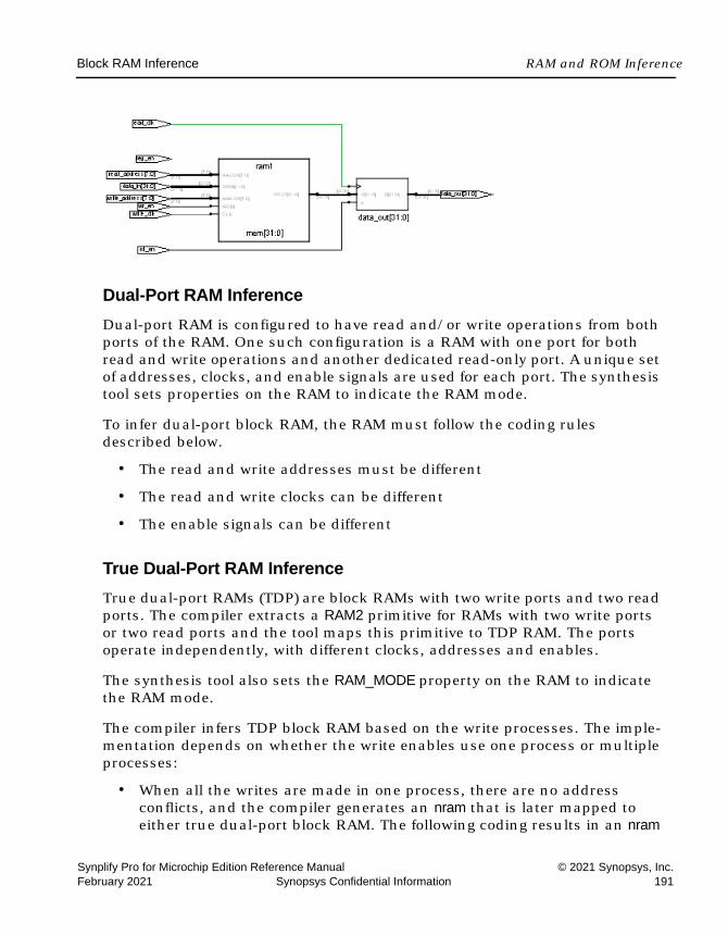
Block RAM Inference RAM and ROM Inference
Synplify Pro for Microchip Edition Reference Manual © 2021 Synopsys, Inc.February 2021 Synopsys Confidential Information 191
Dual-Port RAM InferenceDual-port RAM is configured to have read and/or write operations from both ports of the RAM. One such configuration is a RAM with one port for both read and write operations and another dedicated read-only port. A unique set of addresses, clocks, and enable signals are used for each port. The synthesis tool sets properties on the RAM to indicate the RAM mode.
To infer dual-port block RAM, the RAM must follow the coding rules described below.
• The read and write addresses must be different
• The read and write clocks can be different
• The enable signals can be different
True Dual-Port RAM Inference True dual-port RAMs (TDP) are block RAMs with two write ports and two read ports. The compiler extracts a RAM2 primitive for RAMs with two write ports or two read ports and the tool maps this primitive to TDP RAM. The ports operate independently, with different clocks, addresses and enables.
The synthesis tool also sets the RAM_MODE property on the RAM to indicate the RAM mode.
The compiler infers TDP block RAM based on the write processes. The imple-mentation depends on whether the write enables use one process or multiple processes:
• When all the writes are made in one process, there are no address conflicts, and the compiler generates an nram that is later mapped to either true dual-port block RAM. The following coding results in an nram

LO
RAM and ROM Inference Block RAM Inference
© 2021 Synopsys, Inc. Synplify Pro for Microchip Edition Reference Manual192 Synopsys Confidential Information February 2021
with two write ports, one with write address waddr0 and the other with write address waddr1:
always @(posedge clk)begin
if(we1) mem[waddr0] <= data1;if(we2) mem[waddr1] <= data2;
end • When the writes are made in multiple processes, the software does not
infer a multiport RAM unless you explicitly specify the syn_ramstyle attri-bute with a value that indicates the kind of RAM to implement, or with the no_rw_check value. If the attribute is not specified as such, the software does not infer an nram, but infers a RAM with multiple write ports. You get a warning about simulation mismatches when the two addresses are the same.
In the following case, the compiler infers an nram with two write ports because the syn_ramstyle attribute is specified. The writes associated with waddr0 and waddr1 are we1 and we2, respectively.
reg [1:0] mem [7:0] /* synthesis syn_ramstyle="no_rw_check" */;always @(posedge clk1)begin
if(we1) mem[waddr0] <= data1;endalways @(posedge clk2)begin
if(we2) mem[waddr1] <= data2; end
True Dual-Port Byte-Enabled RAM InferenceThe procedure below describes how to specify RAM where you can read/write each byte into a specific address location independently, and how to imple-ment it as block RAM. See the article 2560210,Verilog RTL Coding Style for True Dual-Port Byte-Enabled RAM on the Synopsys website, for an example.
1. Instantiate the true dual-port RAM n number of times, where n is the number of bytes for a particular RAM address.
In the following example, ram_dp is instantiated twice because there are two bytes in the address:
Block RAM Inference RAM and ROM Inference
Synplify Pro for Microchip Edition Reference Manual © 2021 Synopsys, Inc.February 2021 Synopsys Confidential Information 193
ram_dp u1 (clk1, clk2, dia[7:0] , addra, wea[0], doa[7:0] , dib[7:0] , addrb, web[0],dob[7:0]);
ram_dp u2 (clk1, clk2, dia[15:8], addra, wea[1], doa[15:8], dib[15:8], addrb,web[1], dob[15:8]);
2. To map the true dual-port RAM into a block RAM, add the syn_ramstyle=”block_ram" attribute to the true dual-port RAM module.
3. Run compile.
The RTL schematic shows two instantiations, as specified.
4. Run map.
After synthesis, check the resource utilization report to make sure that two block RAMs were inferred, as specified.
Block RAM ExamplesThe examples below show you how to define RAM in the HDL code so that the synthesis tools can infer block RAM. See the following for details:
• Block RAM Mode Examples, on page 193
• Single-Port Block RAM Examples, on page 197
• Dual-Port Block RAM Examples, on page 200
• True Dual-Port RAM Examples, on page 202
For details about inferring block RAM, see Block RAM Inference, on page 187.
Block RAM Mode ExamplesThe coding style supports the enable and reset pins of the block RAM primi-tive. The tool supports different write mode operations for single-port and dual-port RAM. This section contains examples of how to specify the supported block RAM output modes:
• WRITE_FIRST Mode Example, on page 194
• READ_FIRST Mode Example, on page 195
• NO_CHANGE Mode Example, on page 196

LO
RAM and ROM Inference Block RAM Inference
© 2021 Synopsys, Inc. Synplify Pro for Microchip Edition Reference Manual194 Synopsys Confidential Information February 2021
WRITE_FIRST Mode Example
This example shows the WRITE_FIRST mode operation with active enable.
module v_rams_02a (clk, we, en, addr, di, dou); input clk; input we; input en; input [5:0] addr; input [63:0] di; output [63:0] dou; reg [63:0] RAM [63:0]; reg [63:0] dou; always @(posedge clk) begin if (en)
begin if (we)
begin RAM[addr] <= di; dou <= di;
end else
dou <= RAM[addr]; end
end always @(posedge clk)if (en & we) RAM[addr] <= di;endmoduleThe following figure shows the RTL view of a WRITE_FIRST mode RAM with output registered. Select the Technology view to see that the RAM is mapped to a block RAM.
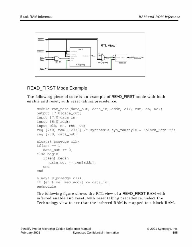
Block RAM Inference RAM and ROM Inference
Synplify Pro for Microchip Edition Reference Manual © 2021 Synopsys, Inc.February 2021 Synopsys Confidential Information 195
READ_FIRST Mode Example
The following piece of code is an example of READ_FIRST mode with both enable and reset, with reset taking precedence:
module ram_test(data_out, data_in, addr, clk, rst, en, we);output [7:0]data_out;input [7:0]data_in;input [6:0]addr;input clk, en, rst, we;reg [7:0] mem [127:0] /* synthesis syn_ramstyle = "block_ram" */;reg [7:0] data_out;always@(posedge clk) if(rst == 1)
data_out <= 0;else begin
if(en) begindata_out <= mem[addr];
endendalways @(posedge clk)if (en & we) mem[addr] <= data_in;endmoduleThe following figure shows the RTL view of a READ_FIRST RAM with inferred enable and reset, with reset taking precedence. Select the Technology view to see that the inferred RAM is mapped to a block RAM.
RTL View
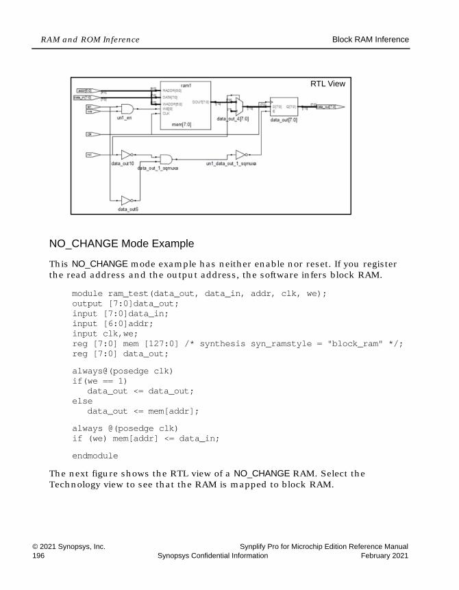
LO
RAM and ROM Inference Block RAM Inference
© 2021 Synopsys, Inc. Synplify Pro for Microchip Edition Reference Manual196 Synopsys Confidential Information February 2021
NO_CHANGE Mode Example
This NO_CHANGE mode example has neither enable nor reset. If you register the read address and the output address, the software infers block RAM.
module ram_test(data_out, data_in, addr, clk, we); output [7:0]data_out; input [7:0]data_in; input [6:0]addr; input clk,we; reg [7:0] mem [127:0] /* synthesis syn_ramstyle = "block_ram" */; reg [7:0] data_out; always@(posedge clk) if(we == 1)
data_out <= data_out; else
data_out <= mem[addr]; always @(posedge clk) if (we) mem[addr] <= data_in; endmodule
The next figure shows the RTL view of a NO_CHANGE RAM. Select the Technology view to see that the RAM is mapped to block RAM.
RTL View
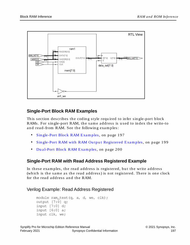
Block RAM Inference RAM and ROM Inference
Synplify Pro for Microchip Edition Reference Manual © 2021 Synopsys, Inc.February 2021 Synopsys Confidential Information 197
Single-Port Block RAM ExamplesThis section describes the coding style required to infer single-port block RAMs. For single-port RAM, the same address is used to index the write-to and read-from RAM. See the following examples:
• Single-Port Block RAM Examples, on page 197
• Single-Port RAM with RAM Output Registered Examples, on page 199
• Dual-Port Block RAM Examples, on page 200
Single-Port RAM with Read Address Registered ExampleIn these examples, the read address is registered, but the write address (which is the same as the read address) is not registered. There is one clock for the read address and the RAM.
Verilog Example: Read Address Registered
module ram_test(q, a, d, we, clk);output [7:0] q;input [7:0] d;input [6:0] a;input clk, we;
RTL View

LO
RAM and ROM Inference Block RAM Inference
© 2021 Synopsys, Inc. Synplify Pro for Microchip Edition Reference Manual198 Synopsys Confidential Information February 2021
reg [6:0] read_add;/* The array of an array register ("mem") from which the RAM is inferred*/reg [7:0] mem [127:0] ;assign q = mem[read_add];always @(posedge clk) beginread_add <= a;if(we)
/* Register RAM Data */mem[a] <= d;
endendmodule
VHDL Example: READ Address Registered
library ieee;use ieee.std_logic_1164.all;use ieee.std_logic_unsigned.all;entity ram_test is
port (d : in std_logic_vector(7 downto 0);a : in std_logic_vector(6 downto 0);we : in std_logic;clk : in std_logic;q : out std_logic_vector(7 downto 0) );
end ram_test;architecture rtl of ram_test istype mem_type is array (127 downto 0) of
std_logic_vector (7 downto 0);signal mem: mem_type;signal read_add : std_logic_vector(6 downto 0);begin
process (clk)begin
if rising_edge(clk) thenif (we = '1') then
mem(conv_integer(a)) <= d;end if;read_add <= a;
end if;end process;
q <= mem(conv_integer(read_add));end rtl ;
Block RAM Inference RAM and ROM Inference
Synplify Pro for Microchip Edition Reference Manual © 2021 Synopsys, Inc.February 2021 Synopsys Confidential Information 199
Single-Port RAM with RAM Output Registered ExamplesIn this example, the RAM output is registered, but the read and write addresses are unregistered. The write address is the same as the read address. There is one clock for the RAM and the output.
Verilog Example: Data Output Registered
module ram_test(q, a, d, we, clk);output [7:0] q;input [7:0] d;input [6:0] a;input clk, we;/* The array of an array register ("mem") from which the RAM is inferred */reg [7:0] mem [127:0] ;reg [7:0] q;always @(posedge clk) beginq = mem[a];if(we)
/* Register RAM Data */mem[a] <= d;
endendmodule
VHDL Example: Data Output Registered
library ieee;use ieee.std_logic_1164.all;use ieee.std_logic_unsigned.all;entity ram_test is
port (d: in std_logic_vector(7 downto 0);a: in integer range 127 downto 0;we: in std_logic;clk: in std_logic;
q: out std_logic_vector(7 downto 0) );end ram_test;architecture rtl of ram_test istype mem_type is array (127 downto 0) of
std_logic_vector (7 downto 0);signal mem: mem_type;begin
LO
RAM and ROM Inference Block RAM Inference
© 2021 Synopsys, Inc. Synplify Pro for Microchip Edition Reference Manual200 Synopsys Confidential Information February 2021
process(clk) begin
if (clk'event and clk='1') thenq <= mem(a);
if (we='1') thenmem(a) <= d;
end if; end if;
end process;end rtl;
Dual-Port Block RAM ExamplesThe following example or HDL code results in simple dual-port block RAMs being implemented in supported technologies.
Verilog Example: Dual-Port RAM
This Verilog example has two read addresses, both of which are registered, and one address for write (same as a read address), which is unregistered. It has two outputs for the RAM, which are unregistered. There is one clock for the RAM and the addresses.
module dualportram ( q1,q2,a1,a2,d,we,clk1) ;output [7:0]q1,q2;input [7:0] d;input [6:0]a1,a2;input clk1,we;wire [7:0] q1;reg [6:0] read_addr1,read_addr2;reg[7:0] mem [127:0] /* synthesis syn_ramstyle = "no_rw_check" */;assign q1 = mem [read_addr1];assign q2 = mem[read_addr2];always @ ( posedge clk1) beginread_addr1 <= a1;read_addr2 <= a2;if (we)
mem[a2] <= d;endendmodule
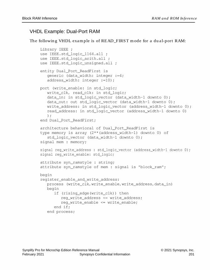
Block RAM Inference RAM and ROM Inference
Synplify Pro for Microchip Edition Reference Manual © 2021 Synopsys, Inc.February 2021 Synopsys Confidential Information 201
VHDL Example: Dual-Port RAM
The following VHDL example is of READ_FIRST mode for a dual-port RAM:
Library IEEE ; use IEEE.std_logic_1164.all ; use IEEE.std_logic_arith.all ; use IEEE.std_logic_unsigned.all ;entity Dual_Port_ReadFirst is
generic (data_width: integer :=4; address_width: integer :=10);
port (write_enable: in std_logic; write_clk, read_clk: in std_logic; data_in: in std_logic_vector (data_width-1 downto 0);data_out: out std_logic_vector (data_width-1 downto 0); write_address: in std_logic_vector (address_width-1 downto 0); read_address: in std_logic_vector (address_width-1 downto 0) );
end Dual_Port_ReadFirst;architecture behavioral of Dual_Port_ReadFirst is type memory is array (2**(address_width-1) downto 0) of
std_logic_vector (data_width-1 downto 0); signal mem : memory;signal reg_write_address : std_logic_vector (address_width-1 downto 0);signal reg_write_enable: std_logic;attribute syn_ramstyle : string; attribute syn_ramstyle of mem : signal is "block_ram";beginregister_enable_and_write_address:
process (write_clk,write_enable,write_address,data_in) begin
if (rising_edge(write_clk)) then reg_write_address <= write_address;reg_write_enable <= write_enable;
end if; end process;
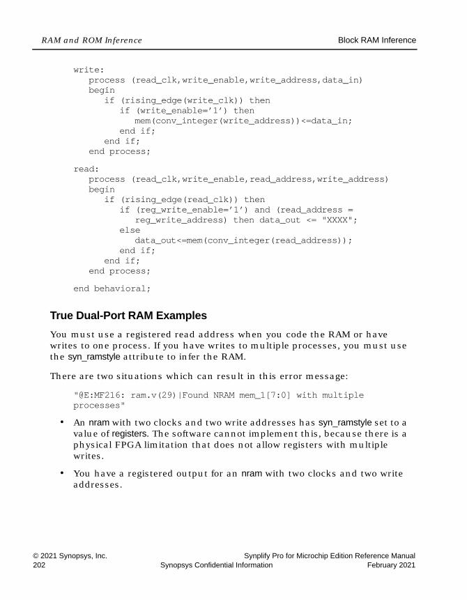
LO
RAM and ROM Inference Block RAM Inference
© 2021 Synopsys, Inc. Synplify Pro for Microchip Edition Reference Manual202 Synopsys Confidential Information February 2021
write: process (read_clk,write_enable,write_address,data_in) begin
if (rising_edge(write_clk)) then if (write_enable=’1’) then
mem(conv_integer(write_address))<=data_in; end if;
end if; end process;
read: process (read_clk,write_enable,read_address,write_address) begin
if (rising_edge(read_clk)) then if (reg_write_enable=’1’) and (read_address =
reg_write_address) then data_out <= "XXXX"; else
data_out<=mem(conv_integer(read_address)); end if;
end if; end process;
end behavioral;
True Dual-Port RAM ExamplesYou must use a registered read address when you code the RAM or have writes to one process. If you have writes to multiple processes, you must use the syn_ramstyle attribute to infer the RAM.
There are two situations which can result in this error message:
"@E:MF216: ram.v(29)|Found NRAM mem_1[7:0] with multiple processes"
• An nram with two clocks and two write addresses has syn_ramstyle set to a value of registers. The software cannot implement this, because there is a physical FPGA limitation that does not allow registers with multiple writes.
• You have a registered output for an nram with two clocks and two write addresses.
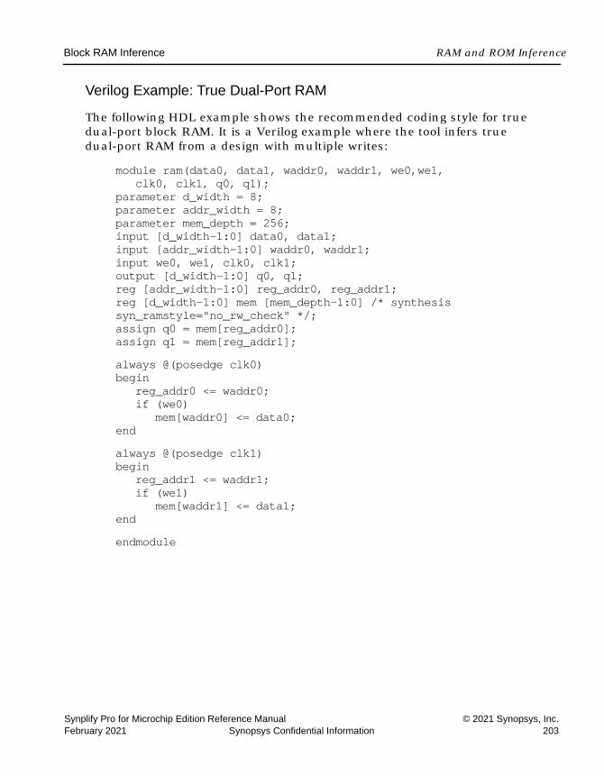
Block RAM Inference RAM and ROM Inference
Synplify Pro for Microchip Edition Reference Manual © 2021 Synopsys, Inc.February 2021 Synopsys Confidential Information 203
Verilog Example: True Dual-Port RAM
The following HDL example shows the recommended coding style for true dual-port block RAM. It is a Verilog example where the tool infers true dual-port RAM from a design with multiple writes:
module ram(data0, data1, waddr0, waddr1, we0,we1,clk0, clk1, q0, q1);
parameter d_width = 8;parameter addr_width = 8;parameter mem_depth = 256; input [d_width-1:0] data0, data1;input [addr_width-1:0] waddr0, waddr1;input we0, we1, clk0, clk1;output [d_width-1:0] q0, q1;reg [addr_width-1:0] reg_addr0, reg_addr1;reg [d_width-1:0] mem [mem_depth-1:0] /* synthesis syn_ramstyle="no_rw_check" */; assign q0 = mem[reg_addr0];assign q1 = mem[reg_addr1]; always @(posedge clk0)begin
reg_addr0 <= waddr0;if (we0)
mem[waddr0] <= data0;end always @(posedge clk1)begin
reg_addr1 <= waddr1;if (we1)
mem[waddr1] <= data1;end endmodule

LO
RAM and ROM Inference Block RAM Inference
© 2021 Synopsys, Inc. Synplify Pro for Microchip Edition Reference Manual204 Synopsys Confidential Information February 2021
VHDL Example: True Dual-Port RAM
The following HDL example shows the recommended coding style for true dual-port block RAM. It is a VHDL example where the tool infers true dual-port RAM from a design with multiple writes:
library ieee;use ieee.std_logic_1164.all;use ieee.numeric_std.all;
entity one isgeneric (data_width : integer := 4;address_width :integer := 5 );
port (data_a:in std_logic_vector(data_width-1 downto 0);data_b:in std_logic_vector(data_width-1 downto 0);addr_a:in std_logic_vector(address_width-1 downto 0);addr_b:in std_logic_vector(address_width-1 downto 0);wren_a:in std_logic;
RTL View

Block RAM Inference RAM and ROM Inference
Synplify Pro for Microchip Edition Reference Manual © 2021 Synopsys, Inc.February 2021 Synopsys Confidential Information 205
wren_b:in std_logic;clk:in std_logic;q_a:out std_logic_vector(data_width-1 downto 0);q_b:out std_logic_vector(data_width-1 downto 0) );
end one;architecture rtl of one istype mem_array is array(0 to 2**(address_width) -1) of std_logic_vector(data_width-1 downto 0);signal mem : mem_array;attribute syn_ramstyle : string;attribute syn_ramstyle of mem : signal is "no_rw_check" ; signal addr_a_reg : std_logic_vector(address_width-1 downto 0);signal addr_b_reg : std_logic_vector(address_width-1 downto 0);begin
WRITE_RAM : process (clk) begin
if rising_edge(clk) thenif (wren_a = '1') then
mem(to_integer(unsigned(addr_a))) <= data_a;end if;if (wren_b='1') then
mem(to_integer(unsigned(addr_b))) <= data_b;end if;addr_a_reg <= addr_a;addr_b_reg <= addr_b;
end if;end process WRITE_RAM;
q_a <= mem(to_integer(unsigned(addr_a_reg)));q_b <= mem(to_integer(unsigned(addr_b_reg)));end rtl;
Limitations to RAM Inference RAM inference is only supported for synchronous RAMs.
// Example 1: Verilog Asymmetric RAM Coding Style 1
module asymmetric_ram (clkA, clkB, weA, enA, addrA, addrB, diA, doB);
parameter WIDTHA = 2;parameter SIZEA = 16384;
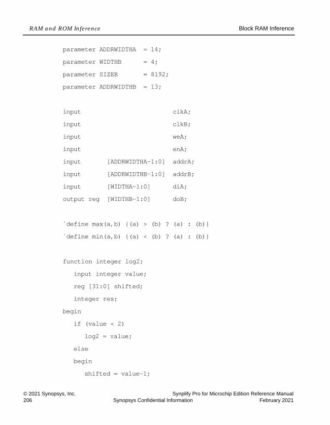
LO
RAM and ROM Inference Block RAM Inference
© 2021 Synopsys, Inc. Synplify Pro for Microchip Edition Reference Manual206 Synopsys Confidential Information February 2021
parameter ADDRWIDTHA = 14;parameter WIDTHB = 4;parameter SIZEB = 8192;parameter ADDRWIDTHB = 13;
input clkA;input clkB;input weA;input enA;input [ADDRWIDTHA-1:0] addrA;input [ADDRWIDTHB-1:0] addrB;input [WIDTHA-1:0] diA;output reg [WIDTHB-1:0] doB;
`define max(a,b) {(a) > (b) ? (a) : (b)}`define min(a,b) {(a) < (b) ? (a) : (b)}
function integer log2;input integer value;reg [31:0] shifted;integer res;
beginif (value < 2)
log2 = value;elsebegin
shifted = value-1;

Block RAM Inference RAM and ROM Inference
Synplify Pro for Microchip Edition Reference Manual © 2021 Synopsys, Inc.February 2021 Synopsys Confidential Information 207
for (res=0; shifted>0; res=res+1)shifted = shifted>>1;
log2 = res;end
endendfunction
localparam maxSIZE = `max(SIZEA, SIZEB);localparam maxWIDTH = `max(WIDTHA, WIDTHB);localparam minWIDTH = `min(WIDTHA, WIDTHB);localparam RATIO = maxWIDTH / minWIDTH;localparam log2RATIO = log2(RATIO);
reg [minWIDTH-1:0] RAM [0:maxSIZE-1];reg [ADDRWIDTHB-1:0] addrB_reg;genvar i;
always @(posedge clkA)begin
if ( enA & weA)RAM[addrA] <= diA;
end
always @(posedge clkB)begin
addrB_reg <= addrB;end
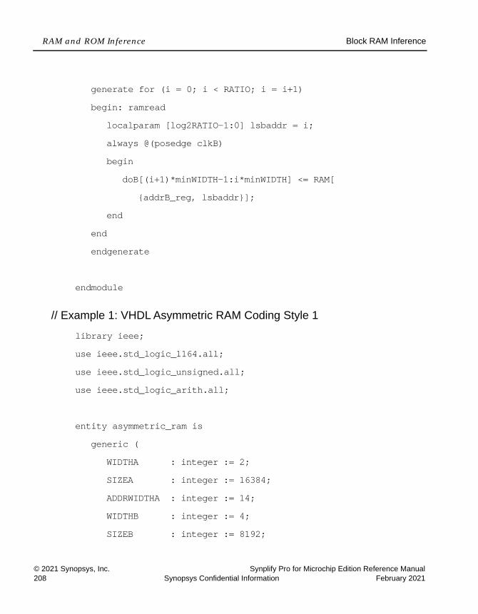
LO
RAM and ROM Inference Block RAM Inference
© 2021 Synopsys, Inc. Synplify Pro for Microchip Edition Reference Manual208 Synopsys Confidential Information February 2021
generate for (i = 0; i < RATIO; i = i+1)begin: ramread
localparam [log2RATIO-1:0] lsbaddr = i;always @(posedge clkB)begin
doB[(i+1)*minWIDTH-1:i*minWIDTH] <= RAM[{addrB_reg, lsbaddr}];
endendendgenerate
endmodule
// Example 1: VHDL Asymmetric RAM Coding Style 1
library ieee;use ieee.std_logic_1164.all;use ieee.std_logic_unsigned.all;use ieee.std_logic_arith.all;
entity asymmetric_ram isgeneric (
WIDTHA : integer := 2;SIZEA : integer := 16384;ADDRWIDTHA : integer := 14;WIDTHB : integer := 4;SIZEB : integer := 8192;
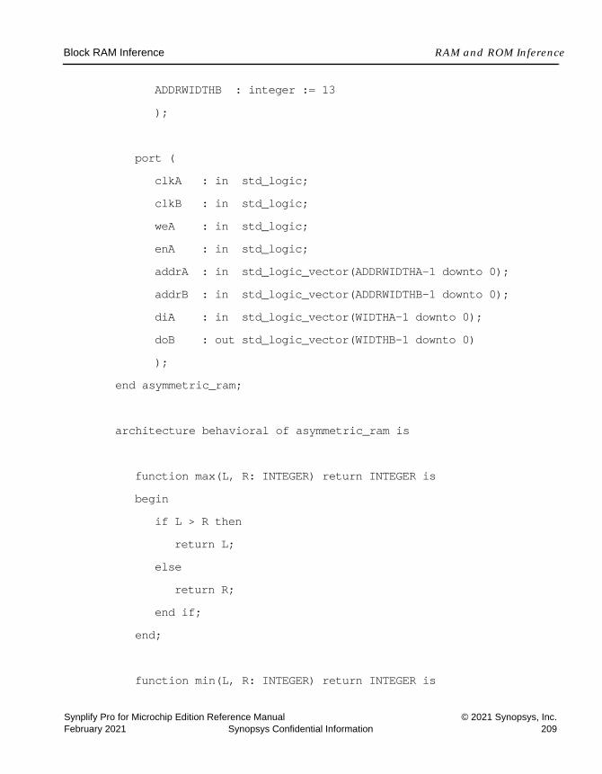
Block RAM Inference RAM and ROM Inference
Synplify Pro for Microchip Edition Reference Manual © 2021 Synopsys, Inc.February 2021 Synopsys Confidential Information 209
ADDRWIDTHB : integer := 13);
port (clkA : in std_logic;clkB : in std_logic;weA : in std_logic;enA : in std_logic;addrA : in std_logic_vector(ADDRWIDTHA-1 downto 0);addrB : in std_logic_vector(ADDRWIDTHB-1 downto 0);diA : in std_logic_vector(WIDTHA-1 downto 0);doB : out std_logic_vector(WIDTHB-1 downto 0));
end asymmetric_ram;
architecture behavioral of asymmetric_ram is
function max(L, R: INTEGER) return INTEGER isbegin
if L > R thenreturn L;
elsereturn R;
end if;end;
function min(L, R: INTEGER) return INTEGER is

LO
RAM and ROM Inference Block RAM Inference
© 2021 Synopsys, Inc. Synplify Pro for Microchip Edition Reference Manual210 Synopsys Confidential Information February 2021
beginif L < R then
return L;else
return R;end if;end;
function log2 (val: INTEGER) return natural isvariable res : natural;
beginfor i in 0 to 31 loop
if (val <= (2**i)) thenres := i;exit;
end if;end loop;return res;
end function Log2;
constant minWIDTH : integer := min(WIDTHA,WIDTHB);constant maxWIDTH : integer := max(WIDTHA,WIDTHB);constant maxSIZE : integer := max(SIZEA,SIZEB);constant RATIO : integer := maxWIDTH / minWIDTH;
type ramType is array (0 to maxSIZE-1) ofstd_logic_vector(minWIDTH-1 downto 0);
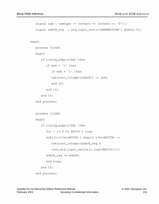
Block RAM Inference RAM and ROM Inference
Synplify Pro for Microchip Edition Reference Manual © 2021 Synopsys, Inc.February 2021 Synopsys Confidential Information 211
signal ram : ramType := (others => (others => ‘0’));signal addrB_reg : std_logic_vector(ADDRWIDTHB-1 downto 0);
beginprocess (clkA)begin
if rising_edge(clkA) thenif enA = ‘1’ then
if weA = ‘1’ thenram(conv_integer(addrA)) <= diA;end if;
end if;end if;
end process;
process (clkB)begin
if rising_edge(clkB) thenfor i in 0 to RATIO-1 loopdoB((i+1)*minWIDTH-1 downto i*minWIDTH) <=
ram(conv_integer(addrB_reg &conv_std_logic_vector(i,log2(RATIO))));
addrB_reg <= addrB;end loop;
end if;end process;
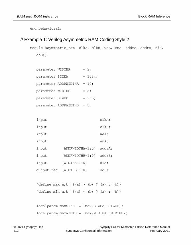
LO
RAM and ROM Inference Block RAM Inference
© 2021 Synopsys, Inc. Synplify Pro for Microchip Edition Reference Manual212 Synopsys Confidential Information February 2021
end behavioral;
// Example 1: Verilog Asymmetric RAM Coding Style 2
module asymmetric_ram (clkA, clkB, weA, enA, addrA, addrB, diA,doB);
parameter WIDTHA = 2;parameter SIZEA = 1024;parameter ADDRWIDTHA = 10;parameter WIDTHB = 8;parameter SIZEB = 256;parameter ADDRWIDTHB = 8;
input clkA;input clkB;input weA;input enA;input [ADDRWIDTHA-1:0] addrA;input [ADDRWIDTHB-1:0] addrB;input [WIDTHA-1:0] diA;output reg [WIDTHB-1:0] doB;
`define max(a,b) {(a) > (b) ? (a) : (b)}`define min(a,b) {(a) < (b) ? (a) : (b)}
localparam maxSIZE = `max(SIZEA, SIZEB);localparam maxWIDTH = `max(WIDTHA, WIDTHB);

Block RAM Inference RAM and ROM Inference
Synplify Pro for Microchip Edition Reference Manual © 2021 Synopsys, Inc.February 2021 Synopsys Confidential Information 213
localparam minWIDTH = `min(WIDTHA, WIDTHB);localparam RATIO = maxWIDTH / minWIDTH;
reg [minWIDTH-1:0] RAM [0:maxSIZE-1];reg [ADDRWIDTHB-1:0] addrB_reg;
always @(posedge clkA)begin
if (weA)begin
RAM[addrA] <= diA;end
end
always @(posedge clkB)begin
addrB_reg <= addrB;doB[4*minWIDTH-1:3*minWIDTH] <= RAM[{addrB_reg, 2’d3}];doB[3*minWIDTH-1:2*minWIDTH] <= RAM[{addrB_reg, 2’d2}];doB[2*minWIDTH-1:minWIDTH] <= RAM[{addrB_reg, 2’d1}];doB[minWIDTH-1:0] <= RAM[{addrB_reg, 2’d0}];
end
endmodule
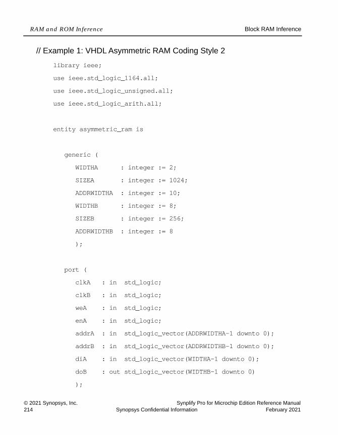
LO
RAM and ROM Inference Block RAM Inference
© 2021 Synopsys, Inc. Synplify Pro for Microchip Edition Reference Manual214 Synopsys Confidential Information February 2021
// Example 1: VHDL Asymmetric RAM Coding Style 2
library ieee;use ieee.std_logic_1164.all;use ieee.std_logic_unsigned.all;use ieee.std_logic_arith.all;
entity asymmetric_ram is
generic (WIDTHA : integer := 2;SIZEA : integer := 1024;ADDRWIDTHA : integer := 10;WIDTHB : integer := 8;SIZEB : integer := 256;ADDRWIDTHB : integer := 8);
port (clkA : in std_logic;clkB : in std_logic;weA : in std_logic;enA : in std_logic;addrA : in std_logic_vector(ADDRWIDTHA-1 downto 0);addrB : in std_logic_vector(ADDRWIDTHB-1 downto 0);diA : in std_logic_vector(WIDTHA-1 downto 0);doB : out std_logic_vector(WIDTHB-1 downto 0));
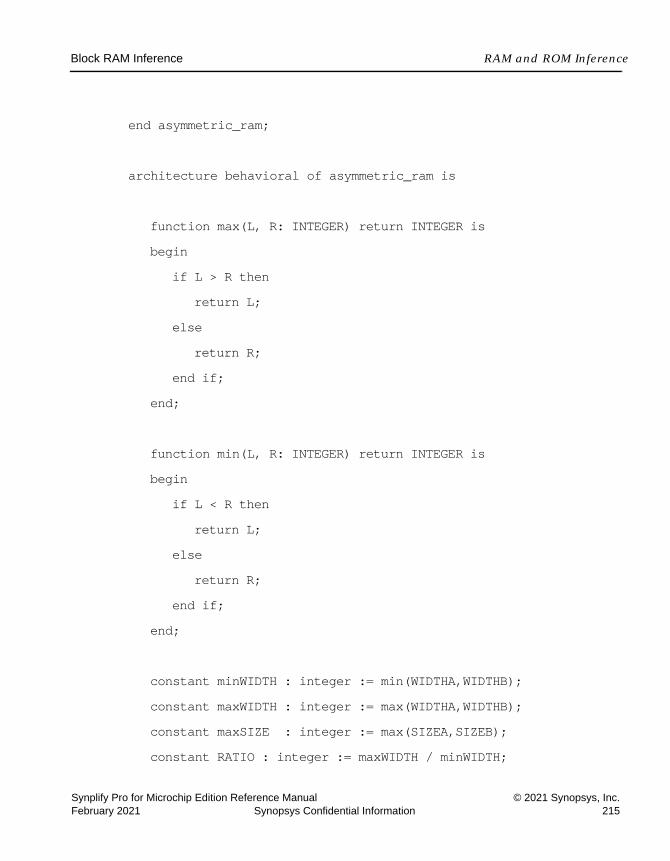
Block RAM Inference RAM and ROM Inference
Synplify Pro for Microchip Edition Reference Manual © 2021 Synopsys, Inc.February 2021 Synopsys Confidential Information 215
end asymmetric_ram;
architecture behavioral of asymmetric_ram is
function max(L, R: INTEGER) return INTEGER isbegin
if L > R thenreturn L;
elsereturn R;
end if;end;
function min(L, R: INTEGER) return INTEGER isbegin
if L < R thenreturn L;
elsereturn R;
end if;end;
constant minWIDTH : integer := min(WIDTHA,WIDTHB);constant maxWIDTH : integer := max(WIDTHA,WIDTHB);constant maxSIZE : integer := max(SIZEA,SIZEB);constant RATIO : integer := maxWIDTH / minWIDTH;
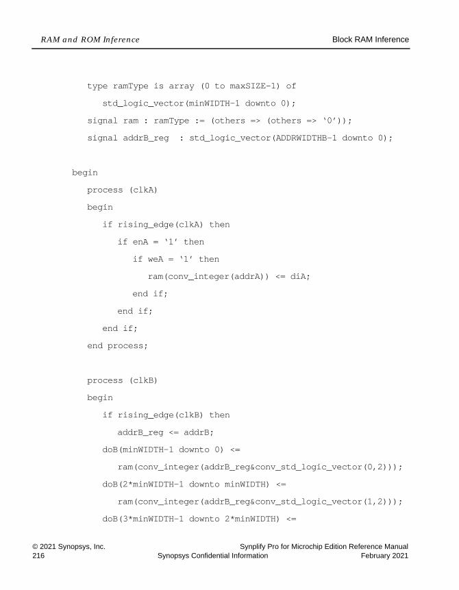
LO
RAM and ROM Inference Block RAM Inference
© 2021 Synopsys, Inc. Synplify Pro for Microchip Edition Reference Manual216 Synopsys Confidential Information February 2021
type ramType is array (0 to maxSIZE-1) ofstd_logic_vector(minWIDTH-1 downto 0);
signal ram : ramType := (others => (others => ‘0’));signal addrB_reg : std_logic_vector(ADDRWIDTHB-1 downto 0);
beginprocess (clkA)begin
if rising_edge(clkA) thenif enA = ‘1’ then
if weA = ‘1’ thenram(conv_integer(addrA)) <= diA;
end if;end if;
end if;end process;
process (clkB)begin
if rising_edge(clkB) thenaddrB_reg <= addrB;
doB(minWIDTH-1 downto 0) <=ram(conv_integer(addrB_reg&conv_std_logic_vector(0,2)));
doB(2*minWIDTH-1 downto minWIDTH) <=ram(conv_integer(addrB_reg&conv_std_logic_vector(1,2)));
doB(3*minWIDTH-1 downto 2*minWIDTH) <=
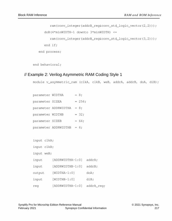
Block RAM Inference RAM and ROM Inference
Synplify Pro for Microchip Edition Reference Manual © 2021 Synopsys, Inc.February 2021 Synopsys Confidential Information 217
ram(conv_integer(addrB_reg&conv_std_logic_vector(2,2))); doB(4*minWIDTH-1 downto 3*minWIDTH) <=
ram(conv_integer(addrB_reg&conv_std_logic_vector(3,2)));end if;
end process;
end behavioral;
// Example 2: Verilog Asymmetric RAM Coding Style 1
module v_asymmetric_ram (clkA, clkB, weB, addrA, addrB, doA, diB);
parameter WIDTHA = 8;parameter SIZEA = 256;parameter ADDRWIDTHA = 8;parameter WIDTHB = 32;parameter SIZEB = 64;parameter ADDRWIDTHB = 6;
input clkA;input clkB;input weB;input [ADDRWIDTHA-1:0] addrA;input [ADDRWIDTHB-1:0] addrB;output [WIDTHA-1:0] doA;input [WIDTHB-1:0] diB;reg [ADDRWIDTHA-1:0] addrA_reg;

LO
RAM and ROM Inference Block RAM Inference
© 2021 Synopsys, Inc. Synplify Pro for Microchip Edition Reference Manual218 Synopsys Confidential Information February 2021
`define max(a,b) {(a) > (b) ? (a) : (b)}`define min(a,b) {(a) < (b) ? (a) : (b)}function integer log2;input integer value;reg [31:0] shifted;integer res;
beginif (value < 2)
log2 = value;elsebeginshifted = value-1;
for (res=0; shifted>0; res=res+1)shifted = shifted>>1;log2 = res;
endend
endfunctionlocalparam maxSIZE = `max(SIZEA, SIZEB);localparam maxWIDTH = `max(WIDTHA, WIDTHB);localparam minWIDTH = `min(WIDTHA, WIDTHB);localparam RATIO = maxWIDTH / minWIDTH;localparam log2RATIO = log2(RATIO);reg [minWIDTH-1:0] RAM [0:maxSIZE-1];reg [WIDTHB-1:0] readB;genvar i;always @(posedge clkA)

Block RAM Inference RAM and ROM Inference
Synplify Pro for Microchip Edition Reference Manual © 2021 Synopsys, Inc.February 2021 Synopsys Confidential Information 219
beginaddrA_reg <= addrA;
endassign doA = RAM[addrA_reg];
generate for (i = 0; i < RATIO; i = i+1)begin: ramread
localparam [log2RATIO-1:0] lsbaddr = i;always @(posedge clkB)beginif (weB)
RAM[{addrB, lsbaddr}] <= diB[(i+1)*minWIDTH-1:i*minWIDTH];
endend
endgenerate
endmodule
// Example 2: VHDL Asymmetric RAM Coding Style 1
library ieee;use ieee.std_logic_1164.all;use ieee.std_logic_unsigned.all;use ieee.std_logic_arith.all;
entity asymmetric_ram isgeneric (
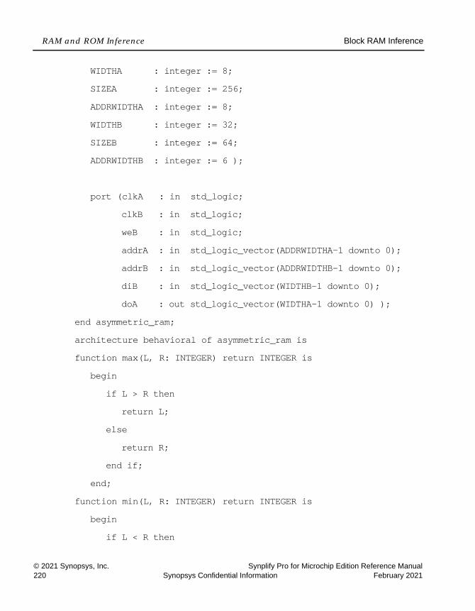
LO
RAM and ROM Inference Block RAM Inference
© 2021 Synopsys, Inc. Synplify Pro for Microchip Edition Reference Manual220 Synopsys Confidential Information February 2021
WIDTHA : integer := 8;SIZEA : integer := 256;ADDRWIDTHA : integer := 8;WIDTHB : integer := 32;SIZEB : integer := 64;ADDRWIDTHB : integer := 6 );
port (clkA : in std_logic;clkB : in std_logic;weB : in std_logic;addrA : in std_logic_vector(ADDRWIDTHA-1 downto 0);addrB : in std_logic_vector(ADDRWIDTHB-1 downto 0);diB : in std_logic_vector(WIDTHB-1 downto 0);doA : out std_logic_vector(WIDTHA-1 downto 0) );
end asymmetric_ram;architecture behavioral of asymmetric_ram isfunction max(L, R: INTEGER) return INTEGER is
beginif L > R then
return L;else
return R;end if;
end;function min(L, R: INTEGER) return INTEGER is
beginif L < R then

Block RAM Inference RAM and ROM Inference
Synplify Pro for Microchip Edition Reference Manual © 2021 Synopsys, Inc.February 2021 Synopsys Confidential Information 221
return L;else
return R;end if;
end;function log2 (val: INTEGER) return natural is
variable res : natural;begin
for i in 0 to 31 loopif (val <= (2**i)) then
res := i;exit;
end if;end loop;
return res;end function Log2;
constant minWIDTH : integer := min(WIDTHA,WIDTHB);constant maxWIDTH : integer := max(WIDTHA,WIDTHB);constant maxSIZE : integer := max(SIZEA,SIZEB);constant RATIO : integer := maxWIDTH / minWIDTH;type ramType is array (0 to maxSIZE-1) ofstd_logic_vector(minWIDTH-1 downto 0);shared variable ram : ramType := (others => (others => ‘0’));signal addrA_reg : std_logic_vector(ADDRWIDTHA-1 downto 0);begin
process (clkA)
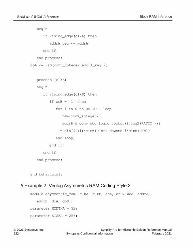
LO
RAM and ROM Inference Block RAM Inference
© 2021 Synopsys, Inc. Synplify Pro for Microchip Edition Reference Manual222 Synopsys Confidential Information February 2021
beginif rising_edge(clkA) then
addrA_reg <= addrA;end if;
end process;doA <= ram(conv_integer(addrA_reg));
process (clkB)begin
if rising_edge(clkB) thenif weB = ‘1’ then
for i in 0 to RATIO-1 loopram(conv_integer(addrB & conv_std_logic_vector(i,log2(RATIO))))
:= diB((i+1)*minWIDTH-1 downto i*minWIDTH);end loop;
end if;end if;
end process;
end behavioral;
// Example 2: Verilog Asymmetric RAM Coding Style 2
module asymmetric_ram (clkA, clkB, enA, enB, weA, addrA, addrB, diA, doB );
parameter WIDTHA = 32;parameter SIZEA = 256;

Block RAM Inference RAM and ROM Inference
Synplify Pro for Microchip Edition Reference Manual © 2021 Synopsys, Inc.February 2021 Synopsys Confidential Information 223
parameter ADDRWIDTHA = 8;parameter WIDTHB= 16;parameter SIZEB = 512;parameter ADDRWIDTHB = 9;
input clkA, clkB, enA, enB, weA; input [ADDRWIDTHA-1:0] addrA;input [ADDRWIDTHB-1:0] addrB;input [WIDTHA-1:0] diA ;output reg [WIDTHB-1:0] doB;reg [WIDTHA-1:0] mux;reg [WIDTHA-1:0] RAM [SIZEA-1:0];always @(posedge clkA)begin
if(enA & weA)RAM[addrA] <= diA;
end
always @(posedge clkB)beginmux = RAM[addrB[ADDRWIDTHB-1:1]];if(enB)
if (addrB[0])begin
doB <= mux[WIDTHA-1:WIDTHB];endelse

LO
RAM and ROM Inference Block RAM Inference
© 2021 Synopsys, Inc. Synplify Pro for Microchip Edition Reference Manual224 Synopsys Confidential Information February 2021
begindoB <= mux[WIDTHB-1:0];
end end
endmodule
// Example 2: VHDL Asymmetric RAM Coding Style 2
library ieee;use ieee.std_logic_1164.all;use ieee.std_logic_unsigned.all;use ieee.std_logic_arith.all;
entity asymmetric_ram isgeneric (
WIDTHA : integer := 32; SIZEA : integer := 256; ADDRWIDTHA : integer := 8; WIDTHB : integer := 16;SIZEB : integer := 512; ADDRWIDTHB : integer := 9
);
port (clkA : in std_logic;clkB : in std_logic;rst : in std_logic;
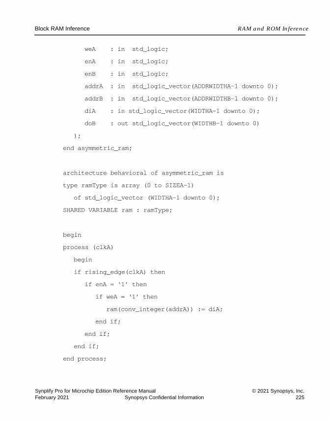
Block RAM Inference RAM and ROM Inference
Synplify Pro for Microchip Edition Reference Manual © 2021 Synopsys, Inc.February 2021 Synopsys Confidential Information 225
weA : in std_logic;enA : in std_logic;enB : in std_logic;addrA : in std_logic_vector(ADDRWIDTHA-1 downto 0);addrB : in std_logic_vector(ADDRWIDTHB-1 downto 0);diA : in std_logic_vector(WIDTHA-1 downto 0);doB : out std_logic_vector(WIDTHB-1 downto 0)
);end asymmetric_ram;
architecture behavioral of asymmetric_ram istype ramType is array (0 to SIZEA-1)
of std_logic_vector (WIDTHA-1 downto 0);SHARED VARIABLE ram : ramType;
beginprocess (clkA)
beginif rising_edge(clkA) then
if enA = ‘1’ then if weA = ‘1’ then
ram(conv_integer(addrA)) := diA;end if;
end if;end if;
end process;

LO
RAM and ROM Inference Block RAM Inference
© 2021 Synopsys, Inc. Synplify Pro for Microchip Edition Reference Manual226 Synopsys Confidential Information February 2021
process (clkB)variable mux : std_logic_vector(WIDTHA-1 downto 0);
beginif rising_edge(clkB) then
if enB = ‘1’ then if addrB(0) = ‘0’ then
mux := ram(conv_integer(addrB(ADDRWIDTHB-1 downto 1)));
doB <= mux (WIDTHB-1 downto 0);else
mux := ram(conv_integer(addrB(ADDRWIDTHB-1 downto 1)));
doB <= mux(WIDTHA-1 downto WIDTHB); end if;
end if;end if;
end process;
end behavioral;
// Example - UltraRAM Inference
// simple dual port, no_change ram, single uram
//synthesis translate_off`define SIMULATION 1//synthesis translate_on

Block RAM Inference RAM and ROM Inference
Synplify Pro for Microchip Edition Reference Manual © 2021 Synopsys, Inc.February 2021 Synopsys Confidential Information 227
`define ADDRSIZE 12`define DATASIZE 72
`ifdef SIMULATION`timescale 1 ps/1 psmodule rtl_ram(din, clk, we, waddr, raddr, dout); `elsemodule synth_ram(din, clk, we, waddr, raddr, dout); `endif input [`DATASIZE-1:0] din; input [`ADDRSIZE-1:0] waddr; input [`ADDRSIZE-1:0] raddr; input clk, we; output [`DATASIZE-1:0] dout;
reg [`ADDRSIZE-1:0] raddr_reg; reg [`DATASIZE-1:0] reg2; reg [`DATASIZE-1:0] reg3; reg [`DATASIZE-1:0] mem [(2**`ADDRSIZE)-1:0];
always @ (posedge clk) begin
if (we) begin mem[waddr] <= din;

LO
RAM and ROM Inference Block RAM Inference
© 2021 Synopsys, Inc. Synplify Pro for Microchip Edition Reference Manual228 Synopsys Confidential Information February 2021
endraddr_reg <= raddr;
end
assign dout = mem[raddr_reg]; endmodule // top
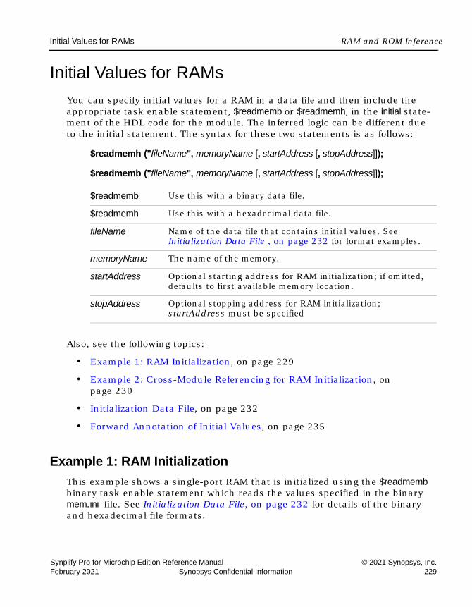
Initial Values for RAMs RAM and ROM Inference
Synplify Pro for Microchip Edition Reference Manual © 2021 Synopsys, Inc.February 2021 Synopsys Confidential Information 229
Initial Values for RAMsYou can specify initial values for a RAM in a data file and then include the appropriate task enable statement, $readmemb or $readmemh, in the initial state-ment of the HDL code for the module. The inferred logic can be different due to the initial statement. The syntax for these two statements is as follows:
$readmemh ("fileName", memoryName [, startAddress [, stopAddress]]);
$readmemb ("fileName", memoryName [, startAddress [, stopAddress]]);
Also, see the following topics:
• Example 1: RAM Initialization, on page 229
• Example 2: Cross-Module Referencing for RAM Initialization, on page 230
• Initialization Data File, on page 232
• Forward Annotation of Initial Values, on page 235
Example 1: RAM Initialization This example shows a single-port RAM that is initialized using the $readmemb binary task enable statement which reads the values specified in the binary mem.ini file. See Initialization Data File, on page 232 for details of the binary and hexadecimal file formats.
$readmemb Use this with a binary data file.
$readmemh Use this with a hexadecimal data file.
fileName Name of the data file that contains initial values. See Initialization Data File , on page 232 for format examples.
memoryName The name of the memory.
startAddress Optional starting address for RAM initialization; if omitted, defaults to first available memory location.
stopAddress Optional stopping address for RAM initialization; startAddress must be specified

LO
RAM and ROM Inference Initial Values for RAMs
© 2021 Synopsys, Inc. Synplify Pro for Microchip Edition Reference Manual230 Synopsys Confidential Information February 2021
module ram_inference (data, clk, addr, we, data_out);input [27:0] data;input clk, we;input [10:0] addr;output [27:0] data_out;reg [27:0] mem [0:2000] /* synthesis syn_ramstyle = "no_rw_check" */;reg [10:0] addr_reg;initialbegin
$readmemb ("mem.ini", mem, 2, 1900) /* Initialize RAM with contents *//* from locations 2 thru 1900*/;
endalways @(posedge clk)begin
addr_reg <= addr;endalways @(posedge clk)begin
if(we)begin
mem[addr] <= data;end
endassign data_out = mem[addr_reg];endmodule
Example 2: Cross-Module Referencing for RAM InitializationThe following example shows how a RAM using cross-module referencing (XMR) can be accessed hierarchically and initialized with the $readmemb/$readmemh statement which reads the values specified in the mem.txt file from the top-level design.
Example2A: XMR for RAM Initialization (Top-Level Module)
// Example 2A: XMR for RAM Initialization (Top-Level Module)
//Top
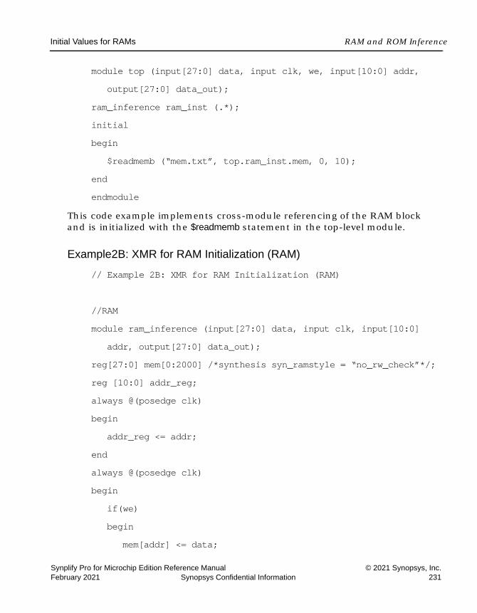
Initial Values for RAMs RAM and ROM Inference
Synplify Pro for Microchip Edition Reference Manual © 2021 Synopsys, Inc.February 2021 Synopsys Confidential Information 231
module top (input[27:0] data, input clk, we, input[10:0] addr,output[27:0] data_out);
ram_inference ram_inst (.*);initialbegin
$readmemb (“mem.txt”, top.ram_inst.mem, 0, 10);endendmodule
This code example implements cross-module referencing of the RAM block and is initialized with the $readmemb statement in the top-level module.
Example2B: XMR for RAM Initialization (RAM)
// Example 2B: XMR for RAM Initialization (RAM)
//RAM module ram_inference (input[27:0] data, input clk, input[10:0]
addr, output[27:0] data_out);reg[27:0] mem[0:2000] /*synthesis syn_ramstyle = “no_rw_check”*/;reg [10:0] addr_reg;always @(posedge clk)begin
addr_reg <= addr;endalways @(posedge clk)begin
if(we)begin
mem[addr] <= data;

LO
RAM and ROM Inference Initial Values for RAMs
© 2021 Synopsys, Inc. Synplify Pro for Microchip Edition Reference Manual232 Synopsys Confidential Information February 2021
endendassign data_out = mem[addr_reg];endmodule
Here is the code example of the RAM block to be implemented for cross-module referencing and initialized.
The following shows the HDL Analyst view of a RAM module that must be accessed hierarchically to be initialized.
RAM Initialization Limitations with XMRXMR for RAM initialization requires that the following conditions be met:
• Variables must be recognized as inferred memories.
• Cross-module referencing of memory variables cannot occur between HDL languages.
• Cross-module referencing paths must be static and cannot include an index with a dynamic value.
Initialization Data FileThe initialization data file, read by the $readmemb and $readmemh system tasks, contains the initial values to be loaded into the memory array. This initialization file can reside in the project directory or can be referenced by an include path relative to the project directory. The system $readmemb or
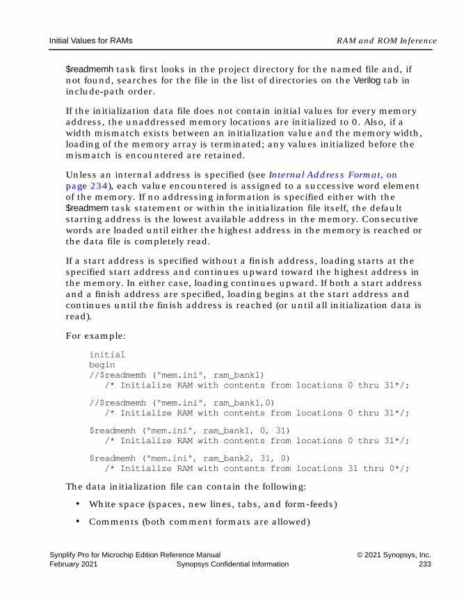
Initial Values for RAMs RAM and ROM Inference
Synplify Pro for Microchip Edition Reference Manual © 2021 Synopsys, Inc.February 2021 Synopsys Confidential Information 233
$readmemh task first looks in the project directory for the named file and, if not found, searches for the file in the list of directories on the Verilog tab in include-path order.
If the initialization data file does not contain initial values for every memory address, the unaddressed memory locations are initialized to 0. Also, if a width mismatch exists between an initialization value and the memory width, loading of the memory array is terminated; any values initialized before the mismatch is encountered are retained.
Unless an internal address is specified (see Internal Address Format, on page 234), each value encountered is assigned to a successive word element of the memory. If no addressing information is specified either with the $readmem task statement or within the initialization file itself, the default starting address is the lowest available address in the memory. Consecutive words are loaded until either the highest address in the memory is reached or the data file is completely read.
If a start address is specified without a finish address, loading starts at the specified start address and continues upward toward the highest address in the memory. In either case, loading continues upward. If both a start address and a finish address are specified, loading begins at the start address and continues until the finish address is reached (or until all initialization data is read).
For example:
initial begin //$readmemh ("mem.ini", ram_bank1)
/* Initialize RAM with contents from locations 0 thru 31*/; //$readmemh ("mem.ini", ram_bank1,0)
/* Initialize RAM with contents from locations 0 thru 31*/;$readmemh ("mem.ini", ram_bank1, 0, 31)
/* Initialize RAM with contents from locations 0 thru 31*/;$readmemh ("mem.ini", ram_bank2, 31, 0)
/* Initialize RAM with contents from locations 31 thru 0*/;The data initialization file can contain the following:
• White space (spaces, new lines, tabs, and form-feeds)
• Comments (both comment formats are allowed)

LO
RAM and ROM Inference Initial Values for RAMs
© 2021 Synopsys, Inc. Synplify Pro for Microchip Edition Reference Manual234 Synopsys Confidential Information February 2021
• Binary values for the $readmemb task, or hexadecimal values for the $readmemh tasks
In addition, the data initialization file can include any number of hexadecimal addresses (see Internal Address Format, on page 234).
Binary File Format
The binary data file mem.ini that corresponds to the example in Example 1: RAM Initialization, on page 229 looks like this:
1111111111111111111100110111 /* data for address 0 */1111111111111111111101100111 /* data for address 1 */1111111111111111111111000010111111111111111111110010000111111111111111111111011100001111111111111111111011100110... /* continues until Address 1999 */
Hex File Format
If you use $readmemh instead of $readmemb, the hexadecimal data file for the example in Example 1: RAM Initialization, on page 229 looks like this:
FFFFF37 /* data for address 0 */FFFFF63 /* data for address 1 */FFFFFC2FFFFF21.../* continues until Address 1999 */
Internal Address Format
In addition to the binary and hex formats described above, the initialization file can include embedded hexadecimal addresses. These hexadecimal addresses must be prefaced with an at sign (@) as shown in the example below.
FFFFF37 /* data for address 0 */FFFFF63 /* data for address 1 */@0EA /* memory address 234FFFFFC2 /* data for address 234*/FFFFF21 /* data for address 235*/

Initial Values for RAMs RAM and ROM Inference
Synplify Pro for Microchip Edition Reference Manual © 2021 Synopsys, Inc.February 2021 Synopsys Confidential Information 235
...@0A7 /* memory address 137FFFFF77 /* data for address 137*/FFFFF7A /* data for address 138*/...
Either uppercase or lowercase characters can be used in the address. No white space is allowed between the @ and the hex address. Any number of address specifications can be included in the file, and in any order. When the $readmemb or $readmemh system task encounters an embedded address speci-fication, it begins loading subsequent data at that memory location.
When addressing information is specified both in the system task and in the data file, the addresses in the data file must be within the address range specified by the system task arguments; otherwise, an error message is issued, and the load operation is terminated.
Forward Annotation of Initial ValuesInitial values for RAMs and sequential shift components are forward annotated to the netlist. The compiler currently generates netlist (srs) files with seqshift, ram1, ram2, and nram components. If initial values are specified in the HDL code, the synthesis tool attaches an attribute to the component in the srs file.
// Example: Verilog Initial Values for Asymmetric RAM
//// Asymmetric port RAM// Port A is 256x8-bit read-only// Port B is 64x32-bit write-only// Write_First mode with no control signals on Address register. Different clocks.//
module v_asymmetric_ram_4 (clkA, clkB, weB, addrA, addrB, doA, diB);
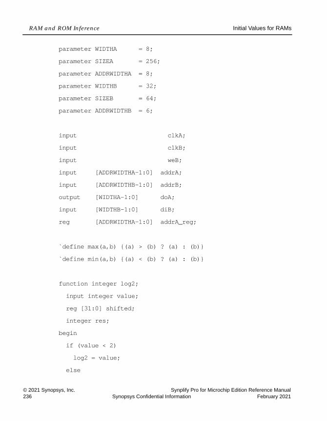
LO
RAM and ROM Inference Initial Values for RAMs
© 2021 Synopsys, Inc. Synplify Pro for Microchip Edition Reference Manual236 Synopsys Confidential Information February 2021
parameter WIDTHA = 8; parameter SIZEA = 256; parameter ADDRWIDTHA = 8; parameter WIDTHB = 32; parameter SIZEB = 64; parameter ADDRWIDTHB = 6; input clkA; input clkB; input weB; input [ADDRWIDTHA-1:0] addrA; input [ADDRWIDTHB-1:0] addrB; output [WIDTHA-1:0] doA; input [WIDTHB-1:0] diB; reg [ADDRWIDTHA-1:0] addrA_reg;
`define max(a,b) {(a) > (b) ? (a) : (b)} `define min(a,b) {(a) < (b) ? (a) : (b)}
function integer log2; input integer value; reg [31:0] shifted; integer res; begin if (value < 2) log2 = value; else

Initial Values for RAMs RAM and ROM Inference
Synplify Pro for Microchip Edition Reference Manual © 2021 Synopsys, Inc.February 2021 Synopsys Confidential Information 237
begin shifted = value-1; for (res=0; shifted>0; res=res+1) shifted = shifted>>1; log2 = res; end end endfunction
localparam maxSIZE = `max(SIZEA, SIZEB); localparam maxWIDTH = `max(WIDTHA, WIDTHB); localparam minWIDTH = `min(WIDTHA, WIDTHB); localparam RATIO = maxWIDTH / minWIDTH; localparam log2RATIO = log2(RATIO); reg [WIDTHB-1:0] readB; genvar i;
reg [minWIDTH-1:0] RAM [0:maxSIZE-1]; // RAM initialization initial $readmemb (“mem_init_256x8.dat”, RAM);
always @(posedge clkA) begin
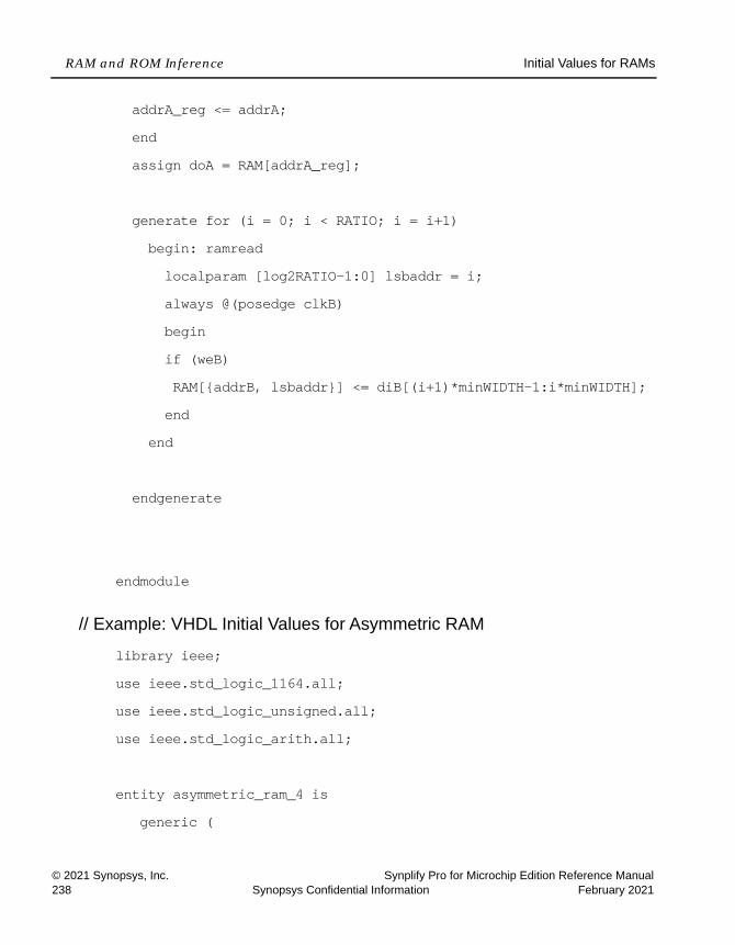
LO
RAM and ROM Inference Initial Values for RAMs
© 2021 Synopsys, Inc. Synplify Pro for Microchip Edition Reference Manual238 Synopsys Confidential Information February 2021
addrA_reg <= addrA; end assign doA = RAM[addrA_reg];
generate for (i = 0; i < RATIO; i = i+1) begin: ramread localparam [log2RATIO-1:0] lsbaddr = i; always @(posedge clkB) begin if (weB) RAM[{addrB, lsbaddr}] <= diB[(i+1)*minWIDTH-1:i*minWIDTH]; end end endgenerate
endmodule
// Example: VHDL Initial Values for Asymmetric RAM
library ieee;use ieee.std_logic_1164.all;use ieee.std_logic_unsigned.all;use ieee.std_logic_arith.all;
entity asymmetric_ram_4 isgeneric (
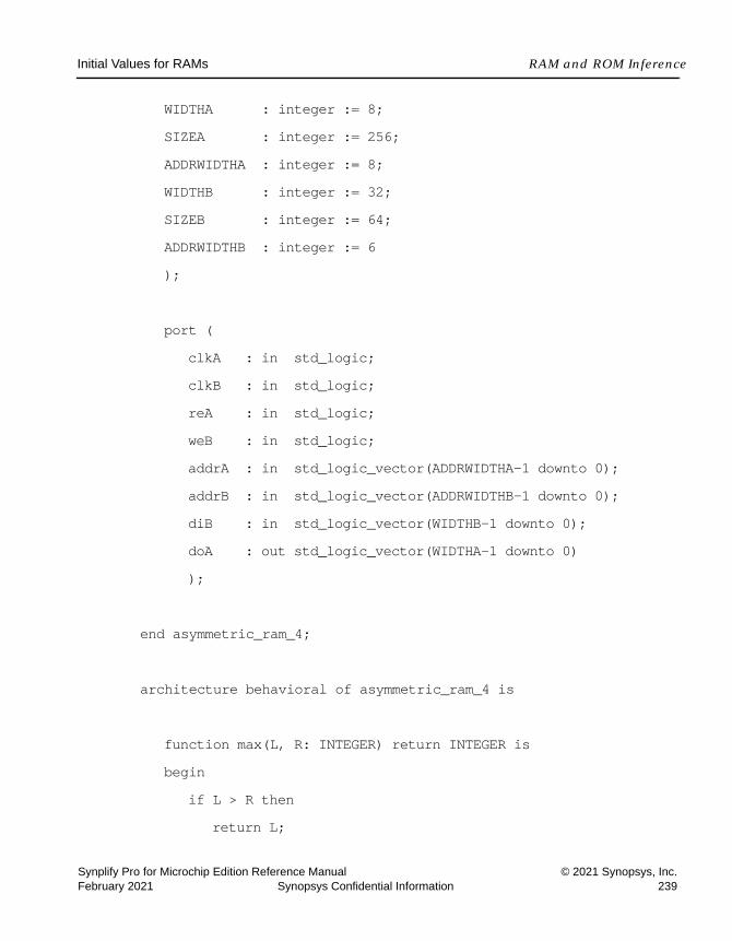
Initial Values for RAMs RAM and ROM Inference
Synplify Pro for Microchip Edition Reference Manual © 2021 Synopsys, Inc.February 2021 Synopsys Confidential Information 239
WIDTHA : integer := 8;SIZEA : integer := 256;ADDRWIDTHA : integer := 8;WIDTHB : integer := 32;SIZEB : integer := 64;ADDRWIDTHB : integer := 6);
port (clkA : in std_logic;clkB : in std_logic;reA : in std_logic;weB : in std_logic;addrA : in std_logic_vector(ADDRWIDTHA-1 downto 0);addrB : in std_logic_vector(ADDRWIDTHB-1 downto 0);diB : in std_logic_vector(WIDTHB-1 downto 0);doA : out std_logic_vector(WIDTHA-1 downto 0));
end asymmetric_ram_4;
architecture behavioral of asymmetric_ram_4 is
function max(L, R: INTEGER) return INTEGER isbegin
if L > R thenreturn L;
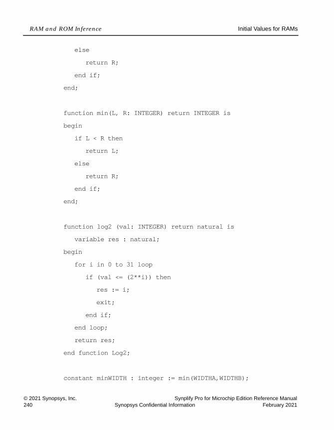
LO
RAM and ROM Inference Initial Values for RAMs
© 2021 Synopsys, Inc. Synplify Pro for Microchip Edition Reference Manual240 Synopsys Confidential Information February 2021
elsereturn R;
end if;end;
function min(L, R: INTEGER) return INTEGER isbegin
if L < R thenreturn L;
elsereturn R;
end if;end;
function log2 (val: INTEGER) return natural isvariable res : natural;
beginfor i in 0 to 31 loop
if (val <= (2**i)) thenres := i;exit;
end if;end loop;return res;
end function Log2;
constant minWIDTH : integer := min(WIDTHA,WIDTHB);
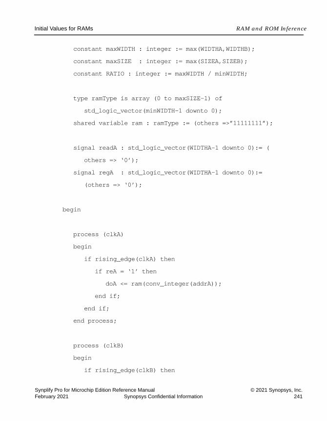
Initial Values for RAMs RAM and ROM Inference
Synplify Pro for Microchip Edition Reference Manual © 2021 Synopsys, Inc.February 2021 Synopsys Confidential Information 241
constant maxWIDTH : integer := max(WIDTHA,WIDTHB);constant maxSIZE : integer := max(SIZEA,SIZEB);constant RATIO : integer := maxWIDTH / minWIDTH;
type ramType is array (0 to maxSIZE-1) ofstd_logic_vector(minWIDTH-1 downto 0);
shared variable ram : ramType := (others =>”11111111”);
signal readA : std_logic_vector(WIDTHA-1 downto 0):= (others => ‘0’);
signal regA : std_logic_vector(WIDTHA-1 downto 0):= (others => ‘0’);
begin
process (clkA)begin
if rising_edge(clkA) thenif reA = ‘1’ then
doA <= ram(conv_integer(addrA));end if;
end if;end process;
process (clkB)begin
if rising_edge(clkB) then

LO
RAM and ROM Inference RAM Instantiation with SYNCORE
© 2021 Synopsys, Inc. Synplify Pro for Microchip Edition Reference Manual242 Synopsys Confidential Information February 2021
if weB = ‘1’ thenfor i in 0 to RATIO-1 loop
ram(conv_integer(addrB &conv_std_logic_vector(i,log2(RATIO))))
:= diB((i+1)*minWIDTH-1 downto i*minWIDTH);end loop;
end if;end if;
end process;
end behavioral;
RAM Instantiation with SYNCOREThe SYNCORE Memory Compiler in the IP Wizard helps you generate HDL code for your specific RAM implementation requirements. For information on using the SYNCORE Memory Compiler, see Chapter 7, SynCore IP Tool

ROM Inference RAM and ROM Inference
Synplify Pro for Microchip Edition Reference Manual © 2021 Synopsys, Inc.February 2021 Synopsys Confidential Information 243
ROM InferenceAs part of BEST (Behavioral Extraction Synthesis Technology) feature, the synthesis tool infers ROMs (read-only memories) from your HDL source code, and generates block components for them in the RTL view.
The data contents of the ROMs are stored in a text file named rom.info. To quickly view rom.info in read-only mode, synthesize your HDL source code, open an RTL view, then push down into the ROM component.
Generally, the Synopsys FPGA synthesis tool infers ROMs from HDL source code that uses case statements, or equivalent if statements, to make 16 or more signal assignments using constant values (words). The constants must all be the same width.
Another requirement for ROM inference is that values must be specified for at least half of the address space. For example, if the ROM has 5 address bits, then the address space is 32 and at least 16 of the different addresses must be specified.
Verilog Examplemodule rom(z,a);output [3:0] z;input [4:0] a;reg [3:0] z;always @(a) begin
case (a)5'b00000 : z = 4'b0001;5'b00001 : z = 4'b0010;5'b00010 : z = 4'b0110;5'b00011 : z = 4'b1010;5'b00100 : z = 4'b1000;5'b00101 : z = 4'b1001;5'b00110 : z = 4'b0000;5'b00111 : z = 4'b1110;5'b01000 : z = 4'b1111;5'b01001 : z = 4'b1110;5'b01010 : z = 4'b0001;5'b01011 : z = 4'b1000;5'b01100 : z = 4'b1110;5'b01101 : z = 4'b0011;5'b01110 : z = 4'b1111;

LO
RAM and ROM Inference ROM Inference
© 2021 Synopsys, Inc. Synplify Pro for Microchip Edition Reference Manual244 Synopsys Confidential Information February 2021
5'b01111 : z = 4'b1100;5'b10000 : z = 4'b1000;5'b10001 : z = 4'b0000;5'b10010 : z = 4'b0011;default : z = 4'b0111;
endcaseendendmodule
VHDL Examplelibrary ieee;use ieee.std_logic_1164.all;entity rom4 is
port (a : in std_logic_vector(4 downto 0);z : out std_logic_vector(3 downto 0) );
end rom4;architecture behave of rom4 isbegin
process(a)begin
if a = "00000" thenz <= "0001";
elsif a = "00001" thenz <= "0010";
elsif a = "00010" thenz <= "0110";
elsif a = "00011" thenz <= "1010";
elsif a = "00100" thenz <= "1000";
elsif a = "00101" thenz <= "1001";
elsif a = "00110" thenz <= "0000";
elsif a = "00111" thenz <= "1110";
elsif a = "01000" thenz <= "1111";
elsif a = "01001" thenz <= "1110";
elsif a = "01010" thenz <= "0001";
elsif a = "01011" then
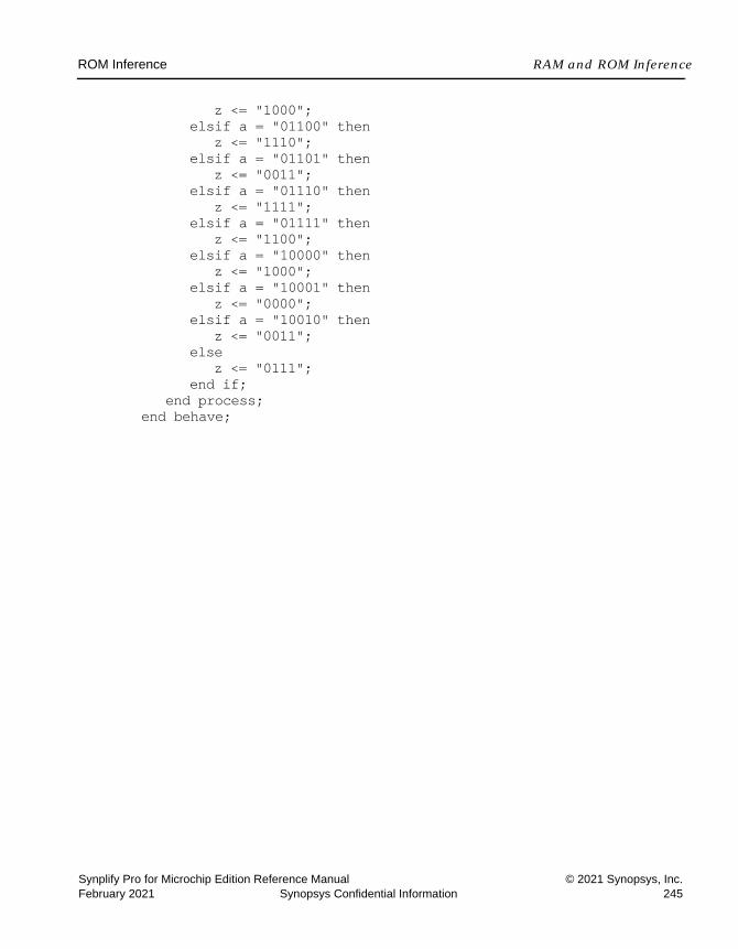
ROM Inference RAM and ROM Inference
Synplify Pro for Microchip Edition Reference Manual © 2021 Synopsys, Inc.February 2021 Synopsys Confidential Information 245
z <= "1000";elsif a = "01100" then
z <= "1110";elsif a = "01101" then
z <= "0011";elsif a = "01110" then
z <= "1111";elsif a = "01111" then
z <= "1100";elsif a = "10000" then
z <= "1000";elsif a = "10001" then
z <= "0000";elsif a = "10010" then
z <= "0011";else
z <= "0111";end if;
end process;end behave;
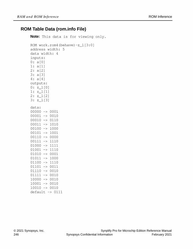
LO
RAM and ROM Inference ROM Inference
© 2021 Synopsys, Inc. Synplify Pro for Microchip Edition Reference Manual246 Synopsys Confidential Information February 2021
ROM Table Data (rom.info File)Note: This data is for viewing only.
ROM work.rom4(behave)-z_1[3:0]address width: 5data width: 4inputs:0: a[0]1: a[1]2: a[2]3: a[3]4: a[4]outputs:0: z_1[0]1: z_1[1]2: z_1[2]3: z_1[3]data:00000 -> 000100001 -> 001000010 -> 011000011 -> 101000100 -> 100000101 -> 100100110 -> 000000111 -> 111001000 -> 111101001 -> 111001010 -> 000101011 -> 100001100 -> 111001101 -> 001101110 -> 001001111 -> 001010000 -> 001010001 -> 001010010 -> 0010default -> 0111

ROM Inference RAM and ROM Inference
Synplify Pro for Microchip Edition Reference Manual © 2021 Synopsys, Inc.February 2021 Synopsys Confidential Information 247
ROM Initialization with Generate BlockThe software supports conditional ROM initialization with the generate block, as shown in the following example:
generateif (INIT) begin
initialbegin
$readmemb("init.hex",mem);end
endendgenerate

LO
RAM and ROM Inference ROM Inference
© 2021 Synopsys, Inc. Synplify Pro for Microchip Edition Reference Manual248 Synopsys Confidential Information February 2021
Synplify Pro for Microchip Edition Reference Manual © 2021 Synopsys, Inc.February 2021 Synopsys Confidential Information 249
C H A P T E R 7
SynCore IP Tool
This chapter describes the SYNCore IP functionality that is bundled with the synthesis tool.
• SYNCore FIFO Compiler, on page 250
• SYNCore RAM Compiler, on page 281
• SYNCore Byte-Enable RAM Compiler, on page 303
• SYNCore ROM Compiler, on page 319
• SYNCore Adder/Subtractor Compiler, on page 334
• SYNCore Counter Compiler, on page 358

LO
SynCore IP Tool SYNCore FIFO Compiler
© 2021 Synopsys, Inc. Synplify Pro for Microchip Edition Reference Manual250 Synopsys Confidential Information February 2021
SYNCore FIFO Compiler The SYNCore synchronous FIFO compiler offers an IP wizard that generates Verilog code for your FIFO implementation. This section describes the following:
• Synchronous FIFO Overview, on page 250
• Specifying FIFOs with SYNCore, on page 251
• SYNCore FIFO Wizard, on page 256
• FIFO Read and Write Operations, on page 265
• FIFO Ports, on page 266
• FIFO Parameters, on page 269
• FIFO Status Flags, on page 271
• FIFO Programmable Flags, on page 274
Synchronous FIFO OverviewA FIFO is a First-In-First-Out memory queue. Different control logic manages the read and write operations. A FIFO also has various handshake signals for interfacing with external user modules.
The SYNCore FIFO compiler generates synchronous FIFOs with symmetric ports and one clock controlling both the read and write operations. The FIFO is symmetric because the read and write ports have the same width.
When the Write_enable signal is active and the FIFO has empty locations, data is written into FIFO memory on the rising edge of the clock. A Full status flag indicates that the FIFO is full and that no more write operations can be performed. See FIFO Write Operation, on page 265 for details.
When the FIFO has valid data and Read_enable is active, data is read from the FIFO memory and presented at the outputs. The FIFO Empty status flag indicates that the FIFO is empty and that no more read operations can be performed. See FIFO Read Operation, on page 266 for details.
The FIFO is not corrupted by an invalid request: for example, if a read request is made while the FIFO is empty or a write request is received when the FIFO is full. Invalid requests do not corrupt the data, but they cause the corre-

SYNCore FIFO Compiler SynCore IP Tool
Synplify Pro for Microchip Edition Reference Manual © 2021 Synopsys, Inc.February 2021 Synopsys Confidential Information 251
sponding read or write request to be ignored and the Overflow or Underflow flags to be asserted. You can monitor these status flags for invalid requests. These and other flags are described in FIFO Status Flags, on page 271 and FIFO Programmable Flags, on page 274.
At any point in time, Data count reflects the available data inside the FIFO. In addition, you can use the Programmable Full and Programmable Empty status flags for user-defined thresholds.
Specifying FIFOs with SYNCore The SYNCore IP Wizard helps you generate Verilog code for your FIFO imple-mentations. The following procedure shows you how to generate Verilog code for a FIFO using the SYNCore IP wizard.
Note: The SYNCore FIFO model uses Verilog 2001. When adding a FIFO model to a Verilog-95 design, be sure to enable the Verilog 2001 check box on the Verilog tab of the Implementation Options dialog box or include a set_option -vlog_std v2001 statement in your project file to prevent a syntax error.
1. Start the wizard.
– From the synthesis tool GUI, select Run->Launch SYNCore or click the Launch SYNCore icon to start the SYNCore IP wizard.

LO
SynCore IP Tool SYNCore FIFO Compiler
© 2021 Synopsys, Inc. Synplify Pro for Microchip Edition Reference Manual252 Synopsys Confidential Information February 2021
– In the window that opens, select sfifo_model and click Ok. This opens the first screen of the wizard.
2. Specify the parameters you need in the five pages of the wizard. For details, refer to Specifying SYNCore FIFO Parameters, on page 254.
The FIFO symbol on the left reflects the parameters you set.
3. After you have specified all the parameters you need, click the Generate button (lower left).
The tool displays a confirmation message (TCL execution successful!) and writes the required files to the directory you specified in the parameters. The HDL code is in Verilog.
The FIFO generated is a synchronous FIFO with symmetric ports and with the same clock controlling both the read and write operations. Data is written or read on the rising edge of the clock. All resets are synchro-

SYNCore FIFO Compiler SynCore IP Tool
Synplify Pro for Microchip Edition Reference Manual © 2021 Synopsys, Inc.February 2021 Synopsys Confidential Information 253
nous with the clock. All edges (clock, enable, and reset) are considered positive.
SYNCore also generates a testbench for the FIFO that you can use for simulation. The testbench covers a limited set of vectors for testing.
You can now close the SYNCore wizard.
4. Add the FIFO you generated to your design.
– Use the Add File command to add the Verilog design file that was generated and the syncore_sfifo.v file to your project. These files are in the directory for output files that you specified on page 1 of the wizard.
– Use a text editor to open the instantiation_file.vin template file, which is located in the same directory. Copy the lines that define the memory, and paste them into your top-level module. The following shows a template file (in red text) inserted into a top-level module.
5. Edit the template port connections so that they agree with the port definitions in your top-level module as shown in the example below (the updated connection names are shown in red). You can also assign a unique name to each instantiation.

LO
SynCore IP Tool SYNCore FIFO Compiler
© 2021 Synopsys, Inc. Synplify Pro for Microchip Edition Reference Manual254 Synopsys Confidential Information February 2021
Note that currently, the FIFO models will not be implemented with the dedicated FIFO blocks available in certain technologies.
Specifying SYNCore FIFO ParametersThe following elaborates on the parameter settings for SYNCore FIFOs. The status, handshaking, and programmable flags are optional. For descriptions of the parameters, see SYNCore FIFO Wizard, on page 256.
1. Start the SYNCore wizard, as described in Specifying FIFOs with SYNCore, on page 251.
2. Do the following on page 1 of the FIFO wizard:
– In Component Name, specify a name for the FIFO. Do not use spaces.
– In Directory, specify a directory where you want the output files to be written. Do not use spaces.
– In Filename, specify a name for the Verilog output file with the FIFO specifications. Do not use spaces.
fifo_a32 busfifo( .Clock(Clk),.Din(DataIn),.Write_enable(WrEn)
,.Dout(DataOut)
endmodule
module top ( input Clk, input [15:0] DataIn,input WrEn,
);
input RdEn,
,.Read_enable(RdEn)
,.Full(Full),.Empty(Empty))
output [15:0] DataOut
output Full,output Empty,

SYNCore FIFO Compiler SynCore IP Tool
Synplify Pro for Microchip Edition Reference Manual © 2021 Synopsys, Inc.February 2021 Synopsys Confidential Information 255
– Click Next. The wizard opens another page where you can set parameters.
3. For a FIFO with no status, handshaking, or programmable flags, use the default settings. You can generate the FIFO, as described in Specifying FIFOs with SYNCore, on page 251.
4. To set an almost full status flag, do the following on page 2 of the FIFO wizard:
– Enable Almost Full. – Set associated handshaking flags for the signal as desired, with the
Overflow Flag and Write Acknowledge options.
– Click Next when you are done.
5. To set an almost empty status flag, do the following on page 3:
– Enable Almost Empty.– Set associated handshaking flags for the signal as desired, with the
Underflow Flag and Read Acknowledge options.
– Click Next when you are done.
6. To set a programmable full flag, do the following:
– Make sure you have enabled Full on page 2 of the wizard and set any handshaking flags you require.
– Go to page 4 and enable Programmable Full.
– Select one of the four mutually exclusive configurations for Programmable Full on page 4. See Programmable Full, on page 275 or details.
– Click Next when you are done.
7. To set a programmable empty flag, do the following:
– Make sure you have enabled Empty on page 3 of the wizard and set any handshaking flags you require.
– Go to page 5 and enable Programmable Empty. – Select one of the four mutually exclusive configurations for
Programmable Empty on page 5. See Programmable Empty, on page 277 or details.
You can now generate the FIFO and add it to the design, as described in Specifying FIFOs with SYNCore, on page 251.
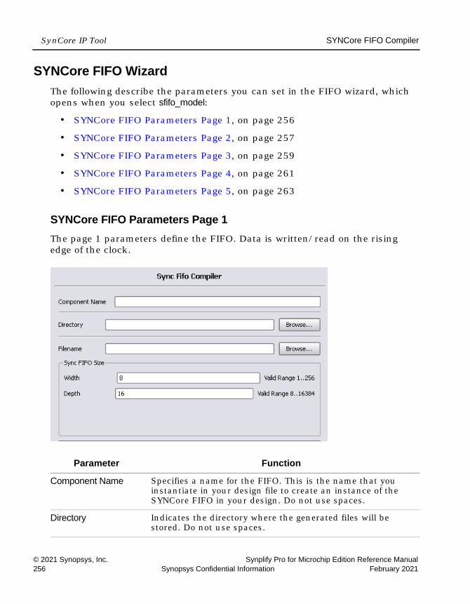
LO
SynCore IP Tool SYNCore FIFO Compiler
© 2021 Synopsys, Inc. Synplify Pro for Microchip Edition Reference Manual256 Synopsys Confidential Information February 2021
SYNCore FIFO WizardThe following describe the parameters you can set in the FIFO wizard, which opens when you select sfifo_model:
• SYNCore FIFO Parameters Page 1, on page 256
• SYNCore FIFO Parameters Page 2, on page 257
• SYNCore FIFO Parameters Page 3, on page 259
• SYNCore FIFO Parameters Page 4, on page 261
• SYNCore FIFO Parameters Page 5, on page 263
SYNCore FIFO Parameters Page 1The page 1 parameters define the FIFO. Data is written/read on the rising edge of the clock.
Parameter Function
Component Name Specifies a name for the FIFO. This is the name that you instantiate in your design file to create an instance of the SYNCore FIFO in your design. Do not use spaces.
Directory Indicates the directory where the generated files will be stored. Do not use spaces.
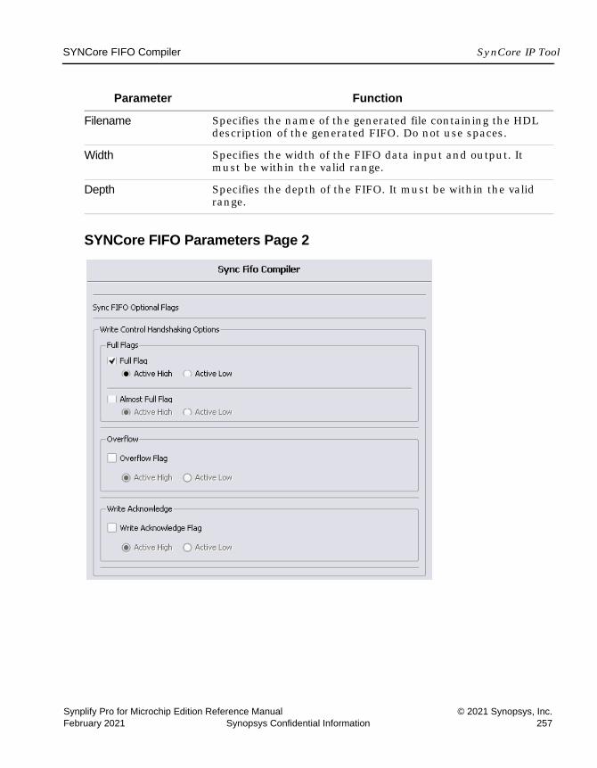
SYNCore FIFO Compiler SynCore IP Tool
Synplify Pro for Microchip Edition Reference Manual © 2021 Synopsys, Inc.February 2021 Synopsys Confidential Information 257
SYNCore FIFO Parameters Page 2
Filename Specifies the name of the generated file containing the HDL description of the generated FIFO. Do not use spaces.
Width Specifies the width of the FIFO data input and output. It must be within the valid range.
Depth Specifies the depth of the FIFO. It must be within the valid range.
Parameter Function
LO
SynCore IP Tool SYNCore FIFO Compiler
© 2021 Synopsys, Inc. Synplify Pro for Microchip Edition Reference Manual258 Synopsys Confidential Information February 2021
The page 2 parameters let you specify optional handshaking flags for FIFO write operations. When you specify a flag, the symbol on the left reflects your choice. Data is written/read on the rising edge of the clock.
Parameter Function
Full Flag Specifies a Full signal, which is asserted when the FIFO memory queue is full and no more writes can be performed until data is read. Enabling this option makes the Active High and Active Low options (FULL_FLAG_SENSE parameter) available for the signal. See Full/Almost Full Flags , on page 271 and FIFO Parameters , on page 269 for descriptions of the flag and parameter.
Almost Full Flag Specifies an Almost_full signal, which is asserted to indicate that there is one location left and the FIFO will be full after one more write operation. Enabling this option makes the Active High and Active Low options available for the signal (AFULL_FLAG_SENSE parameter). See Full/Almost Full Flags , on page 271 and FIFO Parameters , on page 269 for descriptions of the flag and parameter.
Overflow Flag Specifies an Overflow signal, which is asserted to indicate that the write operation was unsuccessful because the FIFO was full. Enabling this option makes the Active High and Active Low options available for the signal (OVERFLOW_FLAG_SENSE parameter). See Handshaking Flags , on page 272 f and FIFO Parameters , on page 269 for descriptions of the flag and parameter.
Write Acknowledge Flag
Specifies a Write_ack signal, which is asserted at the completion of a successful write operation. Enabling this option makes the Active High and Active Low options (WACK_FLAG_SENSE parameter) available for the signal. See Handshaking Flags , on page 272 and FIFO Parameters , on page 269 for descriptions of the flag and parameter.
Active High Sets the specified signal to active high (1).
Active Low Sets the specified signal to active low (0).

SYNCore FIFO Compiler SynCore IP Tool
Synplify Pro for Microchip Edition Reference Manual © 2021 Synopsys, Inc.February 2021 Synopsys Confidential Information 259
SYNCore FIFO Parameters Page 3The page 3 parameters let you specify optional handshaking flags for FIFO read operations. Data is written/read on the rising edge of the clock.
Parameter Function
Empty Flag Specifies an Empty signal, which is asserted when the memory queue for the FIFO is empty and no more reads can be performed until data is written. Enabling this option makes the Active High and Active Low options (EMPTY_FLAG_SENSE parameter) available for the signal. See Empty/Almost Empty Flags , on page 272 and FIFO Parameters , on page 269 for descriptions of the flag and parameter.

LO
SynCore IP Tool SYNCore FIFO Compiler
© 2021 Synopsys, Inc. Synplify Pro for Microchip Edition Reference Manual260 Synopsys Confidential Information February 2021
Almost Empty Flag Specifies an Almost_empty signal, which is asserted when there is only one location left to be read. The FIFO will be empty after one more read operation. Enabling this option makes the Active High and Active Low options (AEMPTY_FLAG_SENSE parameter) available for the signal. See Empty/Almost Empty Flags , on page 272 and FIFO Parameters , on page 269 for descriptions of the flag and parameter.
Underflow Flag Specifies an Underflow signal, which is asserted to indicate that the read operation was unsuccessful because the FIFO was empty. Enabling this option makes the Active High and Active Low options (UNDRFLW_FLAG_SENSE parameter) available for the signal. See Handshaking Flags , on page 272 and FIFO Parameters , on page 269 for descriptions of the flag and parameter.
Read Acknowledge Flag
Specifies a Read_ack signal, which is asserted at the completion of a successful read operation. Enabling this option makes the Active High and Active Low options (RACK_FLAG_SENSE parameter) available for the signal. See Handshaking Flags , on page 272 and FIFO Parameters , on page 269 for descriptions of the flag and parameter.
Active High Sets the specified signal to active high (1).
Active Low Sets the specified signal to active low (0).
Parameter Function

SYNCore FIFO Compiler SynCore IP Tool
Synplify Pro for Microchip Edition Reference Manual © 2021 Synopsys, Inc.February 2021 Synopsys Confidential Information 261
SYNCore FIFO Parameters Page 4
The page 4 parameters let you specify optional handshaking flags for FIFO programmable full operations. To use these options, you must have a Full signal specified. See FIFO Programmable Flags, on page 274 for details and FIFO Parameters, on page 269 for a list of the FIFO parameters. Data is written/read on the rising edge of the clock.
Parameter Function
Programmable Full Flag
Specifies a Prog_full signal, which indicates that the FIFO has reached a user-defined full threshold.You can only enable this option if you set Full Flag on page 2. When it is enabled, you can specify other options for the Prog_Full signal (PFULL_FLAG_SENSE parameter). See Programmable Full , on page 275 and FIFO Parameters , on page 269 for descriptions of the flag and parameter.
LO
SynCore IP Tool SYNCore FIFO Compiler
© 2021 Synopsys, Inc. Synplify Pro for Microchip Edition Reference Manual262 Synopsys Confidential Information February 2021
Single Programmable Full Threshold Constant
Specifies a Prog_full signal with a single constant defining the assertion threshold (PGM_FULL_TYPE=1 parameter). See Programmable Full with Single Threshold Constant , on page 275 for details. Enabling this option makes Full Threshold Assert Constant available.
Multiple Programmable Full Threshold Constant
Specifies a Prog_full signal (PGM_FULL_TYPE=2 parameter), with multiple constants defining the assertion and de-assertion thresholds. See Programmable Full with Multiple Threshold Constants , on page 276 for details. Enabling this option makes Full Threshold Assert Constant and Full Threshold Negate Constant available.
Full Threshold Assert Constant
Specifies a constant that is used as a threshold value for asserting the Prog_full signal It sets the PGM_FULL_THRESH parameter for PGM_FULL_TYPE=1 and the PGM_FULL_ATHRESH parameter for PGM_FULL_TYPE=2.
Full Threshold Negate Constant
Specifies a constant that is used as a threshold value for de-asserting the Prog_full signal (PGM_FULL_NTHRESH parameter).
Single Programmable Full Threshold Input
Specifies a Prog_full signal (PGM_FULL_TYPE=3 parameter), with a threshold value specified dynamically through a Prog_full_thresh input port during the reset state. See Programmable Full with Single Threshold Input , on page 276 for details. Enabling this option adds the Prog_full_thresh input port to the FIFO.
Multiple Programmable Full Threshold Input
Specifies a Prog_full signal (PGM_FULL_TYPE=4 parameter), with threshold assertion and deassertion values specified dynamically through input ports during the reset state. See Programmable Full with Multiple Threshold Inputs , on page 276 for details.Enabling this option adds the Prog_full_thresh_assert and Prog_full_thresh_negate input ports to the FIFO.
Active High Sets the specified signal to active high (1).
Active Low Sets the specified signal to active low (0).
Parameter Function

SYNCore FIFO Compiler SynCore IP Tool
Synplify Pro for Microchip Edition Reference Manual © 2021 Synopsys, Inc.February 2021 Synopsys Confidential Information 263
SYNCore FIFO Parameters Page 5These options specify optional handshaking flags for FIFO programmable empty operations. To use these options, you first specify an Empty signal on page 3. See FIFO Programmable Flags, on page 274 for details and FIFO Param-eters, on page 269 for a list of the FIFO parameters. Data is written/read on the rising edge of the clock.
Parameter Function
Programmable Empty Flag
Specifies a Prog_empty signal (PEMPTY_FLAG_SENSE parameter), which indicates that the FIFO has reached a user-defined empty threshold. See Programmable Empty , on page 277 and FIFO Parameters , on page 269 for descriptions of the flag and parameter. Enabling this option makes the other options available to specify the threshold value, either as a constant or through input ports. You can also specify single or multiple thresholds for each of these options.

LO
SynCore IP Tool SYNCore FIFO Compiler
© 2021 Synopsys, Inc. Synplify Pro for Microchip Edition Reference Manual264 Synopsys Confidential Information February 2021
Single Programmable Empty Threshold Constant
Specifies a Prog_empty signal (PGM_EMPTY_TYPE=1 parameter), with a single constant defining the assertion threshold. See Programmable Empty with Single Threshold Input , on page 279 for details. Enabling this option makes Empty Threshold Assert Constant available.
Multiple Programmable Empty Threshold Constant
Specifies a Prog_empty signal (PGM_EMPTY_TYPE=2 parameter), with multiple constants defining the assertion and de-assertion thresholds. See Programmable Empty with Multiple Threshold Constants , on page 278 for details. Enabling this option makes Empty Threshold Assert Constant and Empty Threshold Negate Constant available.
Empty Threshold Assert Constant
Specifies a constant that is used as a threshold value for asserting the Prog_empty signal. It sets the PGM_EMPTY_THRESH parameter for PGM_EMPTY_TYPE=1 and the PGM_EMPTY_ATHRESH parameter for PGM_EMPTY_TYPE=2.
Empty Threshold Negate Constant
Specifies a constant that is used as a threshold value for de-asserting the Prog_empty signal (PGM_EMPTY_NTHRESH parameter).
Single Programmable Empty Threshold Input
Specifies a Prog_empty signal (PGM_EMPTY_TYPE=3 parameter), with a threshold value specified dynamically through a Prog_empty_thresh input port during the reset state. See Programmable Empty with Single Threshold Input , on page 279 for details. Enabling this option adds the Prog_full_thresh input port to the FIFO.
Multiple Programmable Empty Threshold Input
Specifies a Prog_empty signal (PGM_EMPTY_TYPE=4 parameter), with threshold assertion and deassertion values specified dynamically through Prog_empty_thresh_assert and Prog_empty_thresh_negate input ports during the reset state. See Programmable Empty with Multiple Threshold Inputs , on page 279 for details. Enabling this option adds the input ports to the FIFO.
Active High Sets the specified signal to active high (1).
Active Low Sets the specified signal to active low (0).
Parameter Function

SYNCore FIFO Compiler SynCore IP Tool
Synplify Pro for Microchip Edition Reference Manual © 2021 Synopsys, Inc.February 2021 Synopsys Confidential Information 265
FIFO Read and Write OperationsThis section describes FIFO behavior with read and write operations.
FIFO Write OperationWhen write enable is asserted and the FIFO is not full, data is added to the FIFO from the input bus (Din) and write acknowledge (Write_ack) is asserted. If the FIFO is continuously written without being read, it will fill with data. The status outputs are asserted when the number of entries in the FIFO is greater than or equal to the corresponding threshold, and should be monitored to avoid overflowing the FIFO.
When the FIFO is full, any attempted write operation fails and the overflow flag is asserted.
The following figure illustrates the write operation. Write acknowledge (Write_ack) is asserted on the next rising clock edge after a valid write opera-tion. When Full is asserted, there can be no more legal write operations. This example shows that asserting Write_enable when Full is high causes the asser-tion of Overflow.
Number of Valid Data in FIFO
Specifies the Data_cnt signal for the FIFO output. This signal contains the number of words in the FIFO in the read domain.
Parameter Function

LO
SynCore IP Tool SYNCore FIFO Compiler
© 2021 Synopsys, Inc. Synplify Pro for Microchip Edition Reference Manual266 Synopsys Confidential Information February 2021
FIFO Read OperationWhen read enable is asserted and the FIFO is not empty, the next data word in the FIFO is driven on the output bus (Dout) and a read valid is asserted. If the FIFO is continuously read without being written, the FIFO will empty. The status outputs are asserted when the number of entries in the FIFO are less than or equal to the corresponding threshold, and should be monitored to avoid underflow of the FIFO. When the FIFO is empty, all read operations fail and the underflow flag is asserted.
If read and write operation occur simultaneously during the empty state, the write operation will be valid and empty, and is de-asserted at the next rising clock edge. There cannot be a legal read operation from an empty FIFO, so the underflow flag is asserted.
The following figure illustrates a typical read operation. If the FIFO is not empty, Read_ack is asserted at the rising clock edge after Read_enable is asserted and the data on Dout is valid. When Empty is asserted, no more read operations can be performed. In this case, initiating a read causes the asser-tion of Underflow on the next rising clock edge, as shown in this figure.
FIFO PortsThe following figure shows the FIFO ports.

SYNCore FIFO Compiler SynCore IP Tool
Synplify Pro for Microchip Edition Reference Manual © 2021 Synopsys, Inc.February 2021 Synopsys Confidential Information 267
Port Name Description
Almost_empty Almost empty flag output (active high). Asserted when the FIFO is almost empty and only one more read can be performed. Can be active high or active low.
Almost_full Almost full flag output (active high). Asserted when only one more write can be performed into the FIFO. Can be active high or active low.
AReset Asynchronous reset input. Resets all internal counters and FIFO flag outputs.
Clock Clock input for write and read. Data is written/read on the rising edge.
Data_cnt Data word count output. Indicates the number of words in the FIFO in the read clock domain.
Din [width:0] Data input word to the FIFO.
Dout [width:0] Data output word from the FIFO.

LO
SynCore IP Tool SYNCore FIFO Compiler
© 2021 Synopsys, Inc. Synplify Pro for Microchip Edition Reference Manual268 Synopsys Confidential Information February 2021
Empty FIFO empty output (active high). Asserted when the FIFO is empty and no additional reads can be performed. Can be active high or active low.
Full FIFO full output (active high). Asserted when the FIFO is full and no additional writes can be performed. Can be active high or active low.
Overflow FIFO overflow output flag (active high). Asserted when the FIFO is full and the previous write was rejected. Can be active high or active low.
Prog_empty Programmable empty output flag (active high). Asserted when the words in the FIFO exceed or equal the programmable empty assert threshold. De-asserted when the number of words is more than the programmable full negate threshold. Can be active high or active low.
Prog_empty_thresh
Programmable FIFO empty threshold input. User-programmable threshold value for the assertion of the Prog_empty flag. Set during reset.
Prog_empty_thresh_assert
Programmable FIFO empty threshold assert input. User-programmable threshold value for the assertion of the Prog_empty flag. Set during reset.
Prog_empty_thresh_negate
Programmable FIFO empty threshold negate input. User programmable threshold value for the de-assertion of the Prog_full flag. Set during reset.
Prog_full Programmable full output flag (active high). Asserted when the words in the FIFO exceed or equal the programmable full assert threshold. De-asserted when the number of words is less than the programmable full negate threshold. Can be active high or active low.
Prog_full_thresh Programmable FIFO full threshold input. User-programmable threshold value for the assertion of the Prog_full flag. Set during reset.
Prog_full_thresh_assert
Programmable FIFO full threshold assert input. User-programmable threshold value for the assertion of the Prog_full flag. Set during reset.
Prog_full_thresh_negate
Programmable FIFO full threshold negate input. User-programmable threshold value for the de-assertion of the Prog_full flag. Set during reset.
Port Name Description
SYNCore FIFO Compiler SynCore IP Tool
Synplify Pro for Microchip Edition Reference Manual © 2021 Synopsys, Inc.February 2021 Synopsys Confidential Information 269
FIFO Parameters
Read_ack Read acknowledge output (active high). Asserted when valid data is read from the FIFO. Can be active high or active low.
Read_enable Read enable output (active high). If the FIFO is not empty, data is read from the FIFO on the next rising edge of the read clock.
Underflow FIFO underflow output flag (active high). Asserted when the FIFO is empty and the previous read was rejected.
Write_ack Write Acknowledge output (active high). Asserted when there is a valid write into the FIFO. Can be active high or active low.
Write_enable Write enable input (active high). If the FIFO is not full, data is written into the FIFO on the next rising edge.
Parameter Description
AEMPTY_FLAG_SENSE FIFO almost empty flag sense 0 Active Low1 Active High
AFULL_FLAG_SENSE FIFO almost full flag sense 0 Active Low1 Active High
DEPTH FIFO depth
EMPTY_FLAG_SENSE FIFO empty flag sense 0 Active Low1 Active High
FULL_FLAG_SENSE FIFO full flag sense 0 Active LowOVERFLOW_1 Active High
OVERFLOW_FLAG_SENSE
FIFO overflow flag sense 0 Active Low1 Active High
Port Name Description

LO
SynCore IP Tool SYNCore FIFO Compiler
© 2021 Synopsys, Inc. Synplify Pro for Microchip Edition Reference Manual270 Synopsys Confidential Information February 2021
PEMPTY_FLAG_SENSE
FIFO programmable empty flag sense0 Active Low1 Active High
PFULL_FLAG_SENSE FIFO programmable full flag sense0 Active Low1 Active High
PGM_EMPTY_ATHRESH
Programmable empty assert threshold for PGM_EMPTY_TYPE=2
PGM_EMPTY_NTHRESH
Programmable empty negate threshold for PGM_EMPTY_TYPE=2
PGM_EMPTY_THRESH Programmable empty threshold for PGM_EMPTY_TYPE=1
PGM_EMPTY_TYPE Programmable empty type. See Programmable Empty , on page 277 for details. 1 Programmable empty with single threshold constant.2 Programmable empty with multiple threshold constant3 Programmable empty with single threshold input4 Programmable empty with multiple threshold input
PGM_FULL_ATHRESH Programmable full assert threshold for PGM_FULL_TYPE=2
PGM_FULL_NTHRESH Programmable full negate threshold for PGM_FULL_TYPE=2
PGM_FULL_THRESH Programmable full threshold for PGM_FULL_TYPE=1
PGM_FULL_TYPE Programmable full type. See Programmable Full , on page 275 for details. 1 Programmable full with single threshold constant2 Programmable full with multiple threshold constant3 Programmable full with single threshold input4 Programmable full with multiple threshold input
RACK_FLAG_SENSE FIFO read acknowledge flag sense 0 Active Low1 Active High
Parameter Description

SYNCore FIFO Compiler SynCore IP Tool
Synplify Pro for Microchip Edition Reference Manual © 2021 Synopsys, Inc.February 2021 Synopsys Confidential Information 271
FIFO Status FlagsYou can set the following status flags for FIFO read and write operations.
• Full/Almost Full Flags, on page 271
• Empty/Almost Empty Flags, on page 272
• Handshaking Flags, on page 272
• Programmable full and empty flags, which are described in Program-mable Full, on page 275 and Programmable Empty, on page 277.
Full/Almost Full FlagsThese flags indicate the status of the FIFO memory queue for write opera-tions:
The following figure displays the behavior of these flags. In this example, asserting Wriite_enable when Almost_full is high causes the assertion of Full on the next rising clock edge.
UNDERFLOW_FLAG_SENSE
FIFO underflow flag sense0 Active Low1 Active High
WACK_FLAG_SENSE FIFO write acknowledge flag sense 0 Active Low1 Active High
WIDTH FIFO data input and data output width
Full Indicates that the FIFO memory queue is full and no more writes can be performed until data is read. Full is synchronous with the clock (Clock). If a write is initiated when Full is asserted, the write does not succeed and the overflow flag is asserted.
Almost_full The almost full flag (Almost_full) indicates that there is one location left and the FIFO will be full after one more write operation. Almost full is synchronous to Clock. This flag is guaranteed to be asserted when the FIFO has one remaining location for a write operation.
Parameter Description
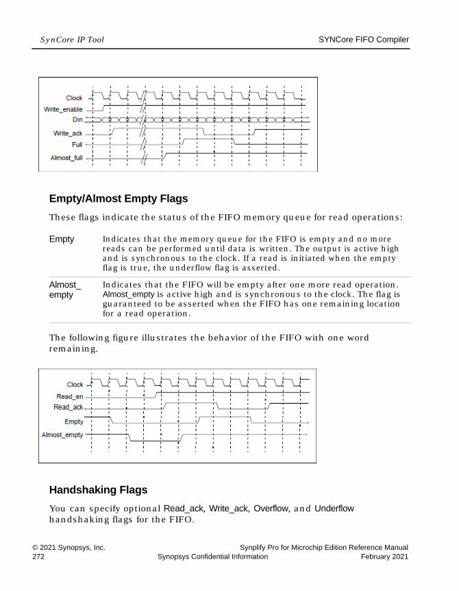
LO
SynCore IP Tool SYNCore FIFO Compiler
© 2021 Synopsys, Inc. Synplify Pro for Microchip Edition Reference Manual272 Synopsys Confidential Information February 2021
Empty/Almost Empty FlagsThese flags indicate the status of the FIFO memory queue for read operations:
The following figure illustrates the behavior of the FIFO with one word remaining.
Handshaking FlagsYou can specify optional Read_ack, Write_ack, Overflow, and Underflow handshaking flags for the FIFO.
Empty Indicates that the memory queue for the FIFO is empty and no more reads can be performed until data is written. The output is active high and is synchronous to the clock. If a read is initiated when the empty flag is true, the underflow flag is asserted.
Almost_empty
Indicates that the FIFO will be empty after one more read operation. Almost_empty is active high and is synchronous to the clock. The flag is guaranteed to be asserted when the FIFO has one remaining location for a read operation.

SYNCore FIFO Compiler SynCore IP Tool
Synplify Pro for Microchip Edition Reference Manual © 2021 Synopsys, Inc.February 2021 Synopsys Confidential Information 273
Read_ack Asserted at the completion of each successful read operation. It indicates that the data on the Dout bus is valid. It is an optional port that is synchronous with Clock and can be configured as active high or active low. Read_ack is deasserted when the FIFO is underflowing, which indicates that the data on the Dout bus is invalid. Read_ack is asserted at the next rising clock edge after read enable. Read_enable is asserted when the FIFO is not empty.
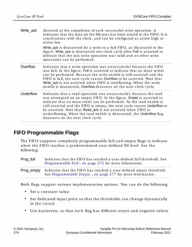
LO
SynCore IP Tool SYNCore FIFO Compiler
© 2021 Synopsys, Inc. Synplify Pro for Microchip Edition Reference Manual274 Synopsys Confidential Information February 2021
FIFO Programmable FlagsThe FIFO supports completely programmable full and empty flags to indicate when the FIFO reaches a predetermined user-defined fill level. See the following:
Both flags support various implementation options. You can do the following:
• Set a constant value
• Set dedicated input ports so that the thresholds can change dynamically in the circuit
• Use hysteresis, so that each flag has different assert and negative values
Write_ack Asserted at the completion of each successful write operation. It indicates that the data on the Din port has been stored in the FIFO. It is synchronous with the clock, and can be configured as active high or active low. Write_ack is deasserted for a write to a full FIFO, as illustrated in the figure. Write_ack is deasserted one clock cycle after Full is asserted to indicate that the last write operation was valid and no other write operations can be performed.
Overflow Indicates that a write operation was unsuccessful because the FIFO was full. In the figure, Full is asserted to indicate that no more writes can be performed. Because the write enable is still asserted and the FIFO is full, the next cycle causes Overflow to be asserted. Note that Write_ack is not asserted when FIFO is overflowing. When the write enable is deasserted, Overflow deasserts on the next clock cycle.
Underflow Indicates that a read operation was unsuccessful, because the read was attempted on an empty FIFO. In the figure, Empty is asserted to indicate that no more reads can be performed. As the read enable is still asserted and the FIFO is empty, the next cycle causes Underflow to be asserted. Note that Read_ack is not asserted when FIFO is underflowing. When the read enable is deasserted, the Underflow flag deasserts on the next clock cycle.
Prog_full Indicates that the FIFO has reached a user-defined full threshold. See Programmable Full , on page 275 for more information.
Prog_empty Indicates that the FIFO has reached a user-defined empty threshold. See Programmable Empty , on page 277 for more information.

SYNCore FIFO Compiler SynCore IP Tool
Synplify Pro for Microchip Edition Reference Manual © 2021 Synopsys, Inc.February 2021 Synopsys Confidential Information 275
Programmable FullThe Prog_full flag (programmable full) is asserted when the number of entries in the FIFO is greater than or equal to a user-defined assert threshold. If the number of words in the FIFO is less than the negate threshold, the flag is de-asserted. The following is the valid range of threshold values:
Prog_full has four threshold types:
• Programmable Full with Single Threshold Constant, on page 275
• Programmable Full with Multiple Threshold Constants, on page 276
• Programmable Full with Single Threshold Input, on page 276
• Programmable Full with Multiple Threshold Inputs, on page 276
Programmable Full with Single Threshold Constant PGM_FULL_TYPE = 1
This option lets you set a single constant value for the threshold. It requires significantly fewer resources when the FIFO is generated. This figure illus-trates the behavior of Prog_full when configured as a single threshold constant with a value of 6.
Assert threshold value
Depth/2 to Max of DepthFor multiple threshold types, the assert value should always be larger than the negate value in multiple threshold types.
Negate threshold value
Depth/2 to Max of Depth
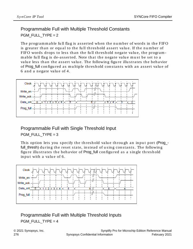
LO
SynCore IP Tool SYNCore FIFO Compiler
© 2021 Synopsys, Inc. Synplify Pro for Microchip Edition Reference Manual276 Synopsys Confidential Information February 2021
Programmable Full with Multiple Threshold Constants PGM_FULL_TYPE = 2
The programmable full flag is asserted when the number of words in the FIFO is greater than or equal to the full threshold assert value. If the number of FIFO words drops to less than the full threshold negate value, the program-mable full flag is de-asserted. Note that the negate value must be set to a value less than the assert value. The following figure illustrates the behavior of Prog_full configured as multiple threshold constants with an assert value of 6 and a negate value of 4.
Programmable Full with Single Threshold Input PGM_FULL_TYPE = 3
This option lets you specify the threshold value through an input port (Prog_-full_thresh) during the reset state, instead of using constants. The following figure illustrates the behavior of Prog_full configured as a single threshold input with a value of 6.
Programmable Full with Multiple Threshold InputsPGM_FULL_TYPE = 4

SYNCore FIFO Compiler SynCore IP Tool
Synplify Pro for Microchip Edition Reference Manual © 2021 Synopsys, Inc.February 2021 Synopsys Confidential Information 277
This option lets you specify the assert and negate threshold values dynami-cally during the reset stage using the Prog_full_thresh_assert and Prog_full_-thresh_negate input ports. You must set the negate value to a value less than the assert value.
The programmable full flag is asserted when the number of words in the FIFO is greater than or equal to the Prog_full_thresh_assert value. If the number of FIFO words goes below Prog_full_thresh_negate value, the programmable full flag is deasserted. The following figure illustrates the behavior of Prog_full configured as multiple threshold inputs with an assert value of 6 and a negate value of 4.
Programmable EmptyThe programmable empty flag (Prog_empty) is asserted when the number of entries in the FIFO is less than or equal to a user-defined assert threshold. If the number of words in the FIFO is greater than the negate threshold, the flag is deasserted. The following is the valid range of threshold values:
There are four threshold types you can specify:
• Programmable Empty with Single Threshold Constant, on page 278
• Programmable Empty with Multiple Threshold Constants, on page 278
• Programmable Empty with Single Threshold Input, on page 279
Assert threshold value
1 to Max of Depth/2For multiple threshold types, the assert value should always be lower than the negate value in multiple threshold types.
Negate threshold value
1 to Max of Depth/2

LO
SynCore IP Tool SYNCore FIFO Compiler
© 2021 Synopsys, Inc. Synplify Pro for Microchip Edition Reference Manual278 Synopsys Confidential Information February 2021
• Programmable Empty with Multiple Threshold Inputs, on page 279
Programmable Empty with Single Threshold ConstantPGM_EMPTY_TYPE = 1
This option lets you specify an empty threshold value with a single constant. This approach requires significantly fewer resources when the FIFO is gener-ated. The following figure illustrates the behavior of Prog_empty configured as a single threshold constant with a value of 3.
Programmable Empty with Multiple Threshold ConstantsPGM_EMPTY_TYPE = 2
This option lets you specify constants for the empty threshold assert value and empty threshold negate value. The programmable empty flag asserts and deasserts in the range set by the assert and negate values. The assert value must be set to a value less than the negate value. When the number of words in the FIFO is less than or equal to the empty threshold assert value, the Prog_empty flag is asserted. When the number of words in FIFO is greater than the empty threshold negate value, Prog_empty is deasserted.
The following figure illustrates the behavior of Prog_empty when configured as multiple threshold constants with an assert value of 3 and a negate value of 5.
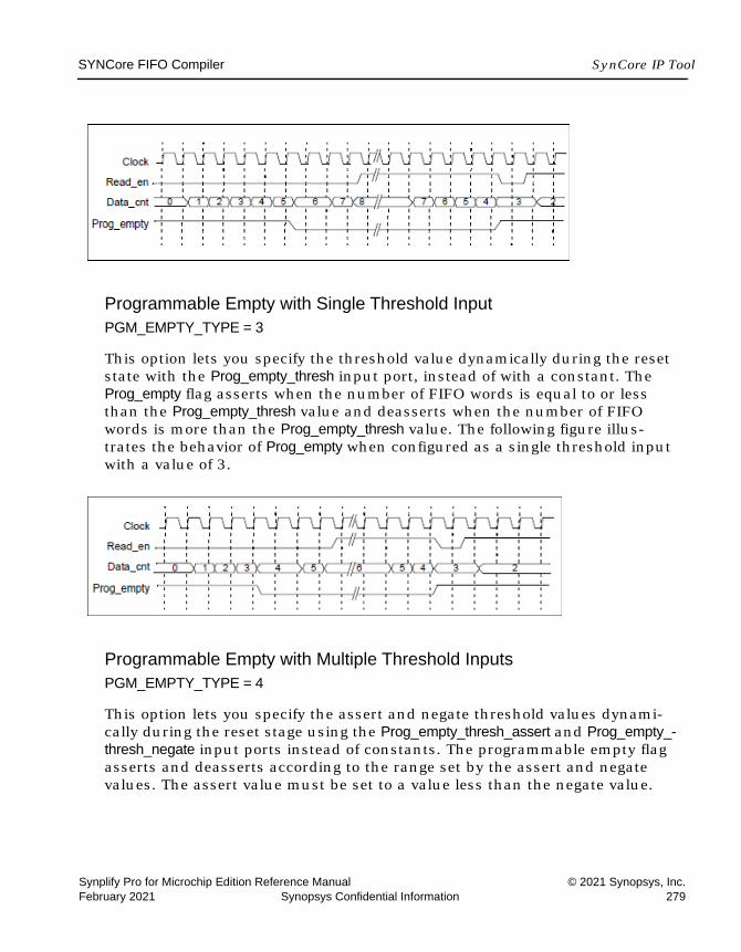
SYNCore FIFO Compiler SynCore IP Tool
Synplify Pro for Microchip Edition Reference Manual © 2021 Synopsys, Inc.February 2021 Synopsys Confidential Information 279
Programmable Empty with Single Threshold InputPGM_EMPTY_TYPE = 3
This option lets you specify the threshold value dynamically during the reset state with the Prog_empty_thresh input port, instead of with a constant. The Prog_empty flag asserts when the number of FIFO words is equal to or less than the Prog_empty_thresh value and deasserts when the number of FIFO words is more than the Prog_empty_thresh value. The following figure illus-trates the behavior of Prog_empty when configured as a single threshold input with a value of 3.
Programmable Empty with Multiple Threshold InputsPGM_EMPTY_TYPE = 4
This option lets you specify the assert and negate threshold values dynami-cally during the reset stage using the Prog_empty_thresh_assert and Prog_empty_-thresh_negate input ports instead of constants. The programmable empty flag asserts and deasserts according to the range set by the assert and negate values. The assert value must be set to a value less than the negate value.

LO
SynCore IP Tool SYNCore FIFO Compiler
© 2021 Synopsys, Inc. Synplify Pro for Microchip Edition Reference Manual280 Synopsys Confidential Information February 2021
When the number of FIFO words is less than or equal to the empty threshold assert value, Prog_empty is asserted. If the number of FIFO words is greater than the empty threshold negate value, the flag is deasserted. The following figure illustrates the behavior of Prog_empty configured as multiple threshold inputs, with an assert value of 3 and a negate value of 5.
SYNCore RAM Compiler SynCore IP Tool
Synplify Pro for Microchip Edition Reference Manual © 2021 Synopsys, Inc.February 2021 Synopsys Confidential Information 281
SYNCore RAM Compiler The SYNCore RAM Compiler generates Verilog code for your RAM implemen-tation. This section describes the following:
• Specifying RAMs with SYNCore, on page 281
• SYNCore RAM Wizard, on page 289
• Single-Port Memories, on page 293
• Dual-Port Memories, on page 295
• Read/Write Timing Sequences, on page 299
Specifying RAMs with SYNCore The SYNCore IP wizard helps you generate Verilog code for your RAM imple-mentation requirements. The following procedure shows you how to generate Verilog code for a RAM using the SYNCore IP wizard.
Note: The SYNCore RAM model uses Verilog 2001. When adding a RAM model to a Verilog-95 design, be sure to enable the Verilog 2001 check box on the Verilog tab of the Implementation Options dialog box or include a set_option -vlog_std v2001 statement in your project file to prevent a syntax error.
1. Start the wizard.
– From the synthesis tool GUI, select Run->Launch SYNCore or click the Launch SYNCore icon to start the SYNCore IP wizard.
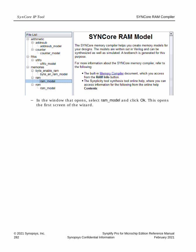
LO
SynCore IP Tool SYNCore RAM Compiler
© 2021 Synopsys, Inc. Synplify Pro for Microchip Edition Reference Manual282 Synopsys Confidential Information February 2021
– In the window that opens, select ram_model and click Ok. This opens the first screen of the wizard.

SYNCore RAM Compiler SynCore IP Tool
Synplify Pro for Microchip Edition Reference Manual © 2021 Synopsys, Inc.February 2021 Synopsys Confidential Information 283
2. Specify the parameters you need in the wizard.
– For details about the parameters for a single-port RAM, see Specifying Parameters for Single-Port RAM, on page 286.
– For details about the parameters for a dual-port RAM, see Specifying Parameters for Dual-Port RAM, on page 287. Note that dual-port implementations are only supported for some technologies.
The RAM symbol on the left reflects the parameters you set.
The default settings for the tool implement a block RAM with synchro-nous resets, and where all edges (clock, enable, and reset) are considered positive.

LO
SynCore IP Tool SYNCore RAM Compiler
© 2021 Synopsys, Inc. Synplify Pro for Microchip Edition Reference Manual284 Synopsys Confidential Information February 2021
3. After you have specified all the parameters you need, click the Generate button in the lower left corner.
The tool displays a confirmation message is displayed (TCL execution successful!) and writes the required files to the directory you specified in the parameters. The HDL code is in Verilog.
SYNCore also generates a testbench for the RAM. The testbench covers a limited set of vectors.
You can now close the SYNCore Memory Compiler.
4. Edit the RAM files if necessary.
– The default RAM has a no_rw_check attribute enabled. If you do not want this, edit syncore_ram.v and comment out the `define SYN_MULTI_PORT_RAM statement, or use `undef SYN_MULTI_PORT_RAM.
– If you want to use the synchronous RAMs available in the target technology, make sure to register either the read address or the outputs.
5. Add the RAM you generated to your design.
– Use the Add File command to add the Verilog design file that was generated and the syncore_ram.v file to your project. These files are in the directory for output files that you specified on page 1 of the wizard.
– Use a text editor to open the instantiation_file.vin template file, which is located in the same directory. Copy the lines that define the memory, and paste them into your top-level module. The following figure shows a template file (in red text) inserted into a top-level module.

SYNCore RAM Compiler SynCore IP Tool
Synplify Pro for Microchip Edition Reference Manual © 2021 Synopsys, Inc.February 2021 Synopsys Confidential Information 285
6. Edit the template port connections so that they agree with the port definitions in your top-level module as shown in the example below (the updated connection names are shown in red). You can also assign a unique name to each instantiation.
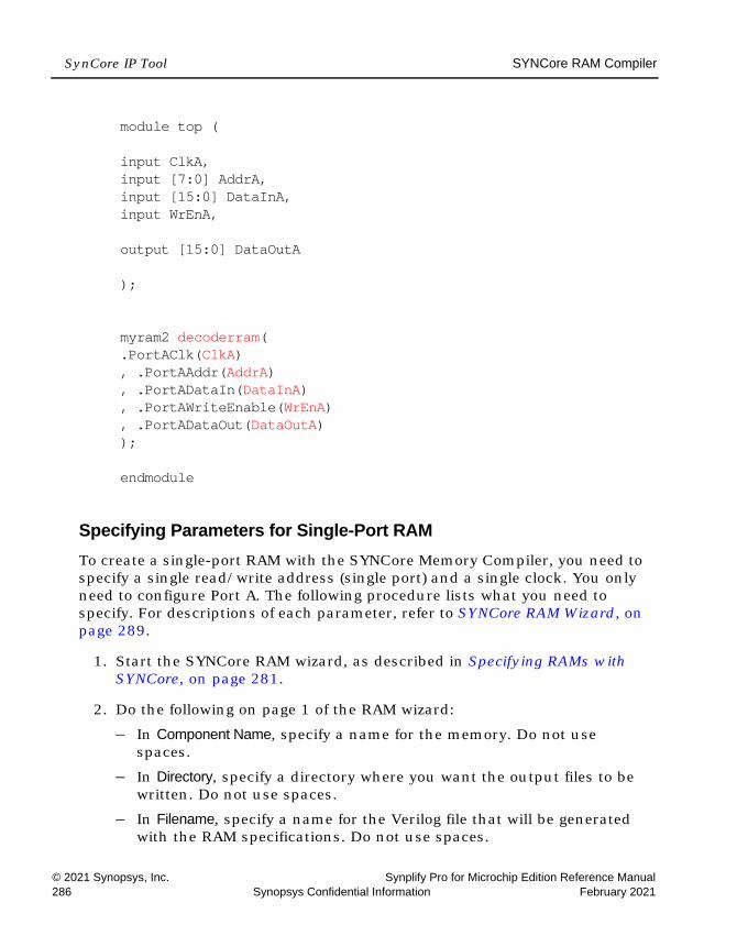
LO
SynCore IP Tool SYNCore RAM Compiler
© 2021 Synopsys, Inc. Synplify Pro for Microchip Edition Reference Manual286 Synopsys Confidential Information February 2021
Specifying Parameters for Single-Port RAMTo create a single-port RAM with the SYNCore Memory Compiler, you need to specify a single read/write address (single port) and a single clock. You only need to configure Port A. The following procedure lists what you need to specify. For descriptions of each parameter, refer to SYNCore RAM Wizard, on page 289.
1. Start the SYNCore RAM wizard, as described in Specifying RAMs with SYNCore, on page 281.
2. Do the following on page 1 of the RAM wizard:
– In Component Name, specify a name for the memory. Do not use spaces.
– In Directory, specify a directory where you want the output files to be written. Do not use spaces.
– In Filename, specify a name for the Verilog file that will be generated with the RAM specifications. Do not use spaces.
module top (
input ClkA, input [7:0] AddrA,input [15:0] DataInA,input WrEnA,
output [15:0] DataOutA
);
myram2 decoderram( .PortAClk(ClkA), .PortAAddr(AddrA), .PortADataIn(DataInA), .PortAWriteEnable(WrEnA), .PortADataOut(DataOutA));
endmodule

SYNCore RAM Compiler SynCore IP Tool
Synplify Pro for Microchip Edition Reference Manual © 2021 Synopsys, Inc.February 2021 Synopsys Confidential Information 287
– Enter data and address widths.
– Enable Single Port, to specify that you want to generate a single-port RAM. This automatically enables Single Clock.
– Click Next. The wizard opens another page where you can set parameters for Port A.
The RAM symbol dynamically updates to reflect the parameters you set.
3. Do the following on page 2 of the RAM wizard:
– Set Use Write Enable to the setting you want.
– Set Register Read Address to the setting you want.
– Set Synchronous Reset to the setting you want. Register Outputs is always enabled
– Specify the read access you require for the RAM.
You can now generate the RAM by clicking Generate, as described in Specifying RAMs with SYNCore, on page 281. You do not need to specify any parameters on page 3, as this is a single-port RAM and you do not need to specify Port B. All output files are in the directory you specified on the first page of the wizard.
For details about setting dual-port RAM parameters, see Specifying Parameters for Dual-Port RAM, on page 287. For read/write timing diagrams, see Read/Write Timing Sequences, on page 299.
Specifying Parameters for Dual-Port RAMThe following procedure shows you how to set parameters for dual-port memory in the SYNCore wizard. Dual-port RAMs are only supported for some technologies. For information about generating single-port RAMs, see Speci-fying Parameters for Single-Port RAM, on page 286. It shows you how to generate these common RAM configurations:
• One read access and one write access
• Two read accesses and one write access
• Two read accesses and two write accesses
For the corresponding read/write timing diagrams, see Read/Write Timing Sequences, on page 299.
LO
SynCore IP Tool SYNCore RAM Compiler
© 2021 Synopsys, Inc. Synplify Pro for Microchip Edition Reference Manual288 Synopsys Confidential Information February 2021
1. Start the SYNCore RAM wizard, as described in Specifying RAMs with SYNCore, on page 281.
2. Do the following on page 1 of the RAM wizard:
– In Component Name, specify a name for the memory. Do not use spaces.
– In Directory, specify a directory where you want the output files to be written. Do not use spaces.
– In Filename, specify a name for the Verilog file that will be generated with the RAM specifications. Do not use spaces.
– Enter data and address widths.
– Enable Dual Port, to specify that you want to generate a dual-port RAM.
– Specify the clocks.
– Click Next. The wizard opens another page where you can set parameters for Port A.
3. Do the following on page 2 of the RAM wizard to specify settings for Port A:
– Set parameters according to the kind of memory you want to generate:
– Specify a setting for Register Read Address.
– Set Synchronous Reset to the setting you want. Register Outputs is always enabled.
For a single clock ... Enable Single Clock.
For separate clocks for each of the ports ...
Enable Separate Clocks For Each Port.
One read & one write Enable Read Only Access.
Two reads & one write Enable Read and Write Access. Specify a setting for Use Write Enable.
Two reads & two writes Enable Read and Write Access. Specify a setting for Use Write Enable. Specify a read access option for Port A.

SYNCore RAM Compiler SynCore IP Tool
Synplify Pro for Microchip Edition Reference Manual © 2021 Synopsys, Inc.February 2021 Synopsys Confidential Information 289
– Click Next. The wizard opens another page where you can set parameters for Port B. The page and the parameters are identical to the previous page, except that the settings are for Port B instead of Port A.
4. Specify the settings for Port B on page 3 of the wizard according to the kind of memory you want to generate:
The RAM symbol on the left reflects the parameters you set. All output files are written to the directory you specified on the first page of the wizard.
You can now generate the RAM by clicking Generate, as described in Specifying RAMs with SYNCore, on page 281, and add it to your design.
SYNCore RAM WizardThe following describe the parameters you can set in the RAM wizard, which opens when you select ram_model:
• SYNCore RAM Parameters Page 1, on page 290
• SYNCore RAM Parameters Pages 2 and 3, on page 292
One read & one write Enable Write Only Access. Set Use Write Enable to the setting you want.
Two reads & one write Enable Read Only Access.Specify a setting for Register Read Address.
Two reads & two writes Enable Read and Write Access. Specify a setting for Use Write Enable. Specify a setting for Register Read Address. Set Synchronous Reset to the setting you want. Note that Register Outputs is always enabled. Select a read access option for Port B.
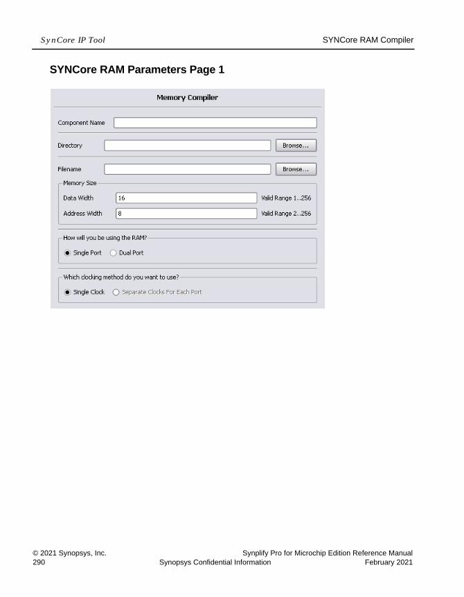
LO
SynCore IP Tool SYNCore RAM Compiler
© 2021 Synopsys, Inc. Synplify Pro for Microchip Edition Reference Manual290 Synopsys Confidential Information February 2021
SYNCore RAM Parameters Page 1
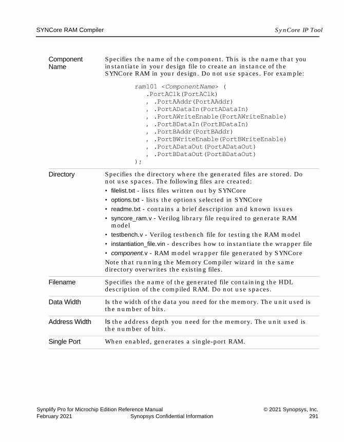
SYNCore RAM Compiler SynCore IP Tool
Synplify Pro for Microchip Edition Reference Manual © 2021 Synopsys, Inc.February 2021 Synopsys Confidential Information 291
Component Name
Specifies the name of the component. This is the name that you instantiate in your design file to create an instance of the SYNCore RAM in your design. Do not use spaces. For example:
ram101 <ComponentName> ( .PortAClk(PortAClk), .PortAAddr(PortAAddr), .PortADataIn(PortADataIn), .PortAWriteEnable(PortAWriteEnable), .PortBDataIn(PortBDataIn) , .PortBAddr(PortBAddr), .PortBWriteEnable(PortBWriteEnable), .PortADataOut(PortADataOut), .PortBDataOut(PortBDataOut)
);Directory Specifies the directory where the generated files are stored. Do
not use spaces. The following files are created:• filelist.txt - lists files written out by SYNCore• options.txt - lists the options selected in SYNCore• readme.txt - contains a brief description and known issues• syncore_ram.v - Verilog library file required to generate RAM
model• testbench.v - Verilog testbench file for testing the RAM model • instantiation_file.vin - describes how to instantiate the wrapper file• component.v - RAM model wrapper file generated by SYNCoreNote that running the Memory Compiler wizard in the same directory overwrites the existing files.
Filename Specifies the name of the generated file containing the HDL description of the compiled RAM. Do not use spaces.
Data Width Is the width of the data you need for the memory. The unit used is the number of bits.
Address Width Is the address depth you need for the memory. The unit used is the number of bits.
Single Port When enabled, generates a single-port RAM.

LO
SynCore IP Tool SYNCore RAM Compiler
© 2021 Synopsys, Inc. Synplify Pro for Microchip Edition Reference Manual292 Synopsys Confidential Information February 2021
SYNCore RAM Parameters Pages 2 and 3The port implementation parameters on pages 2 and 3 are identical, but page 2 applies to Port A (single- and dual-port configurations), and page 3 applies to Port B (dual-port configurations only). The following figure shows the parameters on page 2 for Port A.
Dual Port When enabled, generates a dual-port RAM.
Single Clock When enabled, generates a RAM with a single clock for dual-port configurations.
Separate Clocks for Each Port
When enabled, generates separate clocks for each port in dual-port RAM configurations.
Read and Write Access
Specifies that the port can be accessed by both read and write operations.
Read Only Access Specifies that the port can only be accessed by read operations.
Write Only Access Specifies that the port can only be accessed by write operations.
Use Write Enable Includes write-enable control. The RAM symbol on the left reflects the selections you make.

SYNCore RAM Compiler SynCore IP Tool
Synplify Pro for Microchip Edition Reference Manual © 2021 Synopsys, Inc.February 2021 Synopsys Confidential Information 293
Single-Port MemoriesFor single-port RAM, it is only necessary to configure Port A. The following diagrams show the read-write timing for single-port memories. See Specifying RAMs with SYNCore, on page 281 for a procedure.
Register Read Address
Adds registers to the read address lines. The RAM symbol on the left reflects the selections you make.
Register Outputs Adds registers to the write address lines when you specify separate read/write addressing. The register outputs are always enabled. The RAM symbol on the left reflects the selections you make.
Synchronous Reset
Individually synchronizes the reset signal with the clock when you enable Register Outputs. The RAM symbol on the left reflects the selections you make.
Read before Write Specifies that the read operation takes place before the write operation for port configurations with both read and write access (Read And Write Access is enabled). For a timing diagram, see Read Before Write , on page 300.
Read after Write Specifies that the read operation takes place after the write operation for port configurations with both read and write access (Read And Write Access is enabled). For a timing diagram, see Write Before Read , on page 301.
No Read on Write Specifies that no read operation takes place when there is a write operation for port configurations with both read and write access (Read And Write Access is enabled). For a timing diagram, see No Read on Write , on page 302.

LO
SynCore IP Tool SYNCore RAM Compiler
© 2021 Synopsys, Inc. Synplify Pro for Microchip Edition Reference Manual294 Synopsys Confidential Information February 2021
Single-Port Read

SYNCore RAM Compiler SynCore IP Tool
Synplify Pro for Microchip Edition Reference Manual © 2021 Synopsys, Inc.February 2021 Synopsys Confidential Information 295
Single-Port Write
Dual-Port MemoriesSYNCore dual-port memory includes the following common configurations:
• One read access and one write access
• Two read accesses and one write access
• Two read accesses and two write accesses
The following diagrams show the read-write timing for dual-port memories. See Specifying RAMs with SYNCore, on page 281 for a procedure to specify a dual-port RAM with SYNCore.
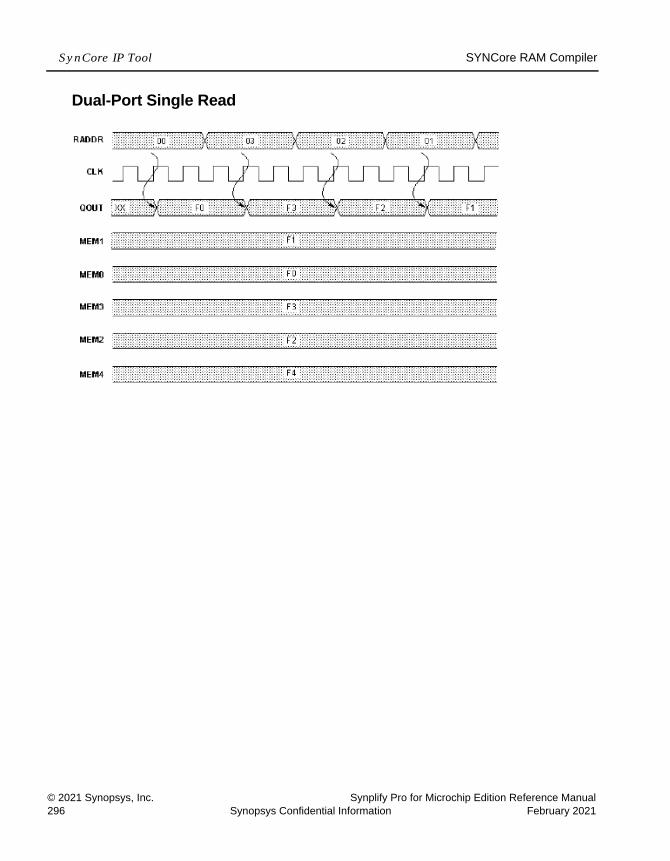
LO
SynCore IP Tool SYNCore RAM Compiler
© 2021 Synopsys, Inc. Synplify Pro for Microchip Edition Reference Manual296 Synopsys Confidential Information February 2021
Dual-Port Single Read
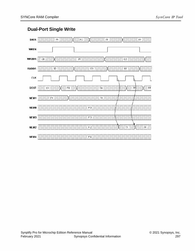
SYNCore RAM Compiler SynCore IP Tool
Synplify Pro for Microchip Edition Reference Manual © 2021 Synopsys, Inc.February 2021 Synopsys Confidential Information 297
Dual-Port Single Write

LO
SynCore IP Tool SYNCore RAM Compiler
© 2021 Synopsys, Inc. Synplify Pro for Microchip Edition Reference Manual298 Synopsys Confidential Information February 2021
Dual-Port Read
SYNCore RAM Compiler SynCore IP Tool
Synplify Pro for Microchip Edition Reference Manual © 2021 Synopsys, Inc.February 2021 Synopsys Confidential Information 299
Dual-Port Write
Read/Write Timing Sequences The waveforms in this section describe the behavior of the RAM when both read and write are enabled and the address is the same operation. The waveforms show the behavior when each of the read-write sequences is enabled. The waveforms are merged with the simple waveforms shown in the previous sections. See the following:
• Read Before Write, on page 300
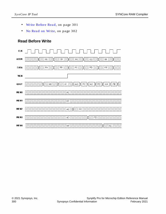
LO
SynCore IP Tool SYNCore RAM Compiler
© 2021 Synopsys, Inc. Synplify Pro for Microchip Edition Reference Manual300 Synopsys Confidential Information February 2021
• Write Before Read, on page 301
• No Read on Write, on page 302
Read Before Write

SYNCore RAM Compiler SynCore IP Tool
Synplify Pro for Microchip Edition Reference Manual © 2021 Synopsys, Inc.February 2021 Synopsys Confidential Information 301
Write Before Read
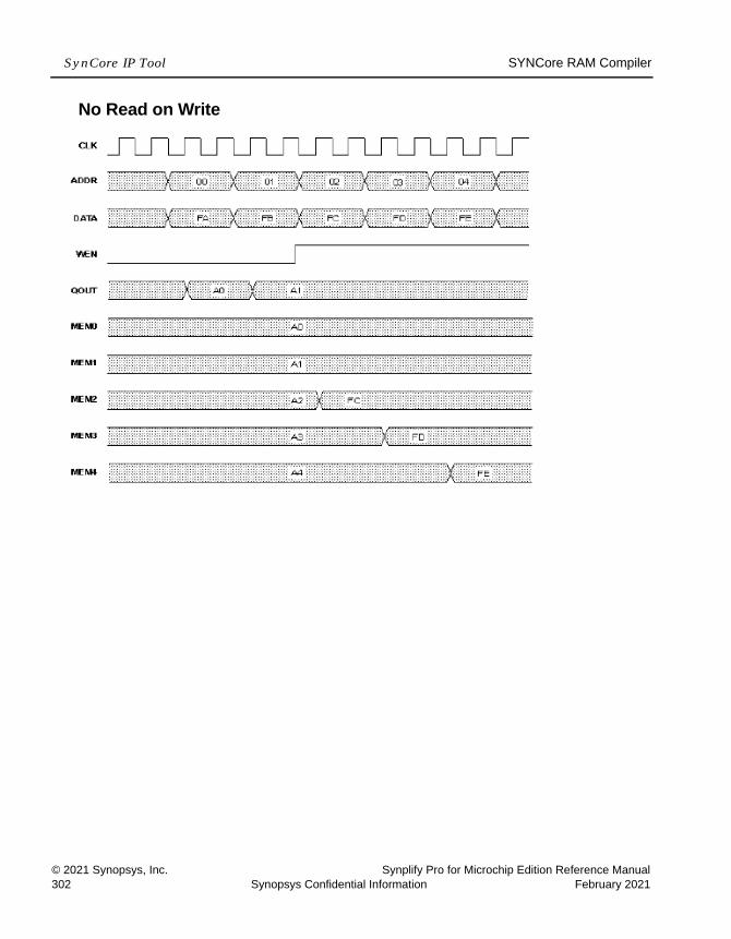
LO
SynCore IP Tool SYNCore RAM Compiler
© 2021 Synopsys, Inc. Synplify Pro for Microchip Edition Reference Manual302 Synopsys Confidential Information February 2021
No Read on Write
SYNCore Byte-Enable RAM Compiler SynCore IP Tool
Synplify Pro for Microchip Edition Reference Manual © 2021 Synopsys, Inc.February 2021 Synopsys Confidential Information 303
SYNCore Byte-Enable RAM Compiler The SYNCore byte-enable RAM compiler generates SystemVerilog code describing byte-enabled RAMs. The data width of each byte is calculated by dividing the total data width by the write enable width. The byte-enable RAM compiler supports both single- and dual-port configurations.
This section describes the following:
• Functional Overview, on page 303
• Specifying Byte-Enable RAMs with SYNCore, on page 304
• SYNCore Byte-Enable RAM Wizard, on page 311
• Read/Write Timing Sequences, on page 314
• Parameter List, on page 317
Functional OverviewThe SYNCore byte-enable RAM component supports bit/byte-enable RAM implementations using block RAM and distributed memory. For each config-uration, design optimizations are made for optimum use of core resources. The timing diagram that follow illustrate the supported signals for byte-enable RAM configurations.
Byte-enable RAM can be configured in both single- and dual-port configura-tions. In the dual-port configuration, each port is controlled by different clock, enable, and control signals. User configuration controls include selecting the enable level, reset type, and register type for the read data outputs and address inputs.
Reset applies only to the output read data registers; default value of read data on reset can be changed by user while generating core. Reset option is inactive when output read data is not registered.
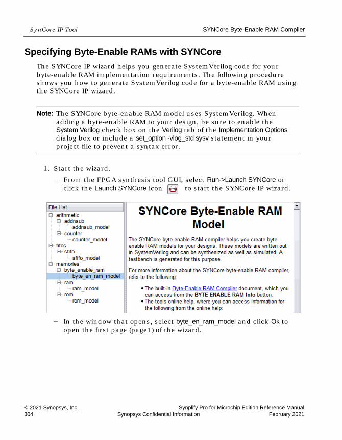
LO
SynCore IP Tool SYNCore Byte-Enable RAM Compiler
© 2021 Synopsys, Inc. Synplify Pro for Microchip Edition Reference Manual304 Synopsys Confidential Information February 2021
Specifying Byte-Enable RAMs with SYNCore The SYNCore IP wizard helps you generate SystemVerilog code for your byte-enable RAM implementation requirements. The following procedure shows you how to generate SystemVerilog code for a byte-enable RAM using the SYNCore IP wizard.
Note: The SYNCore byte-enable RAM model uses SystemVerilog. When adding a byte-enable RAM to your design, be sure to enable the System Verilog check box on the Verilog tab of the Implementation Options dialog box or include a set_option -vlog_std sysv statement in your project file to prevent a syntax error.
1. Start the wizard.
– From the FPGA synthesis tool GUI, select Run->Launch SYNCore or click the Launch SYNCore icon to start the SYNCore IP wizard.
– In the window that opens, select byte_en_ram_model and click Ok to open the first page (page1) of the wizard.

SYNCore Byte-Enable RAM Compiler SynCore IP Tool
Synplify Pro for Microchip Edition Reference Manual © 2021 Synopsys, Inc.February 2021 Synopsys Confidential Information 305
2. Specify the parameters you need in the wizard. For details about the parameters, see Specifying Byte-Enable RAM Parameters, on page 308. The BYTE ENABLE RAM symbol on the left reflects any parameters you set.
3. After you have specified all the parameters you need, click the Generate button in the lower left corner. The tool displays a confirmation message (TCL execution successful!) and writes the required files to the directory you specified on page 1 of the wizard. The HDL code is in SystemVerilog.
SYNCore also generates a test bench for the byte-enable RAM compo-nent. The test bench covers a limited set of vectors. You can now close the SYNCore byte-enable RAM compiler.
4. Edit the generated files for the byte-enable RAM component if necessary.
5. Add the byte-enable RAM that you generated to your design.
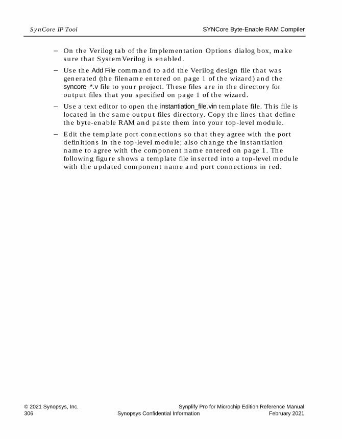
LO
SynCore IP Tool SYNCore Byte-Enable RAM Compiler
© 2021 Synopsys, Inc. Synplify Pro for Microchip Edition Reference Manual306 Synopsys Confidential Information February 2021
– On the Verilog tab of the Implementation Options dialog box, make sure that SystemVerilog is enabled.
– Use the Add File command to add the Verilog design file that was generated (the filename entered on page 1 of the wizard) and the syncore_*.v file to your project. These files are in the directory for output files that you specified on page 1 of the wizard.
– Use a text editor to open the instantiation_file.vin template file. This file is located in the same output files directory. Copy the lines that define the byte-enable RAM and paste them into your top-level module.
– Edit the template port connections so that they agree with the port definitions in the top-level module; also change the instantiation name to agree with the component name entered on page 1. The following figure shows a template file inserted into a top-level module with the updated component name and port connections in red.

SYNCore Byte-Enable RAM Compiler SynCore IP Tool
Synplify Pro for Microchip Edition Reference Manual © 2021 Synopsys, Inc.February 2021 Synopsys Confidential Information 307
Port ListPort A interface signals are applicable for both single-port and dual-port configurations; Port B signals are applicable for dual-port configuration only.
Name Type Description
ClkA Input Clock input for Port A
WenA Input Write enable for Port A; present when Port A is in write mode
AddrA Input Memory access address for Port A

LO
SynCore IP Tool SYNCore Byte-Enable RAM Compiler
© 2021 Synopsys, Inc. Synplify Pro for Microchip Edition Reference Manual308 Synopsys Confidential Information February 2021
Specifying Byte-Enable RAM ParametersWhen creating a single-port, byte-enable RAM with the SYNCore IP wizard, you must specify a single read address and a single clock; you only need to configure the Port A parameters on page 2 of the wizard.
When creating a dual-port, byte-enable RAM, you must additionally configure the Port B parameters on page 3 of the wizard.
The following procedure lists the parameters you need to specify. For descrip-tions of each parameter, refer to Parameter List, on page 317.
1. Start the SYNCore byte-enable RAM wizard as described in Specifying Byte-Enable RAMs with SYNCore, on page 304.
ResetA Input Reset for memory and all registers in core; present with registered read data when Reset is enabled; active low (cannot be changed)
WrDataA Input Write data to memory for Port A; present when Port A is in write mode
RdDataA Output Read data output for Port A; present when Port A is in read or read/write mode
ClkB Input Clock input for Port B; present in dual-port mode
WenB Input Write enable for Port B; present in dual-port mode when Port B is in write mode
AddrB Input Memory access address for Port B; present in dual-port mode
ResetB Input Reset for memory and all registers in core; present in dual-port mode when read data is registered and Reset is enabled; active low (cannot be changed)
WrDataB Input Write data to memory for Port B; present in dual-port mode when Port B is in write mode
RdDataB Output Read data output for Port B; present in dual-port mode when Port B is in read or read/write mode

SYNCore Byte-Enable RAM Compiler SynCore IP Tool
Synplify Pro for Microchip Edition Reference Manual © 2021 Synopsys, Inc.February 2021 Synopsys Confidential Information 309
2. Do the following on page 1 of the byte-enable RAM wizard:
– Specify a name for the memory in the Component Name field; do not use spaces.
– Specify a directory name in the Directory field where you want the output files to be written; do not use spaces.
– Specify a name in the File Name field for the SystemVerilog file to be generated with the byte-enable RAM specifications; do not use spaces.
– Enter a value for the address width of the byte-enable RAM; the maximum depth of memory is limited to 2^256.
– Enter a value for the data width for the byte-enable RAM; data width values range from 2 to 256.
– Enter a value for the write enable width; write-enable width values range from 1 to 4.
– Select Single Port to generate a single-port, byte-enable RAM or select Dual Port to generate a dual-port, byte-enable RAM.
– Click Next to open page 2 of the wizard.
The Byte Enable RAM symbol dynamically updates to reflect the param-eters that you set.

LO
SynCore IP Tool SYNCore Byte-Enable RAM Compiler
© 2021 Synopsys, Inc. Synplify Pro for Microchip Edition Reference Manual310 Synopsys Confidential Information February 2021
3. Do the following on page 2 (configuring Port A) of the wizard:
– Select the Port A configuration. Only Read and Write Access mode is valid for single-port configurations; this mode is selected by default.
– Set Pipelining Address Bus and Output Data according to your application. By default, read data is registered; you can register both the address and data registers.
– Set the Configure Reset Options. Enabling the checkbox enables the synchronous reset for read data. This option is enabled only when the read data is registered. Reset is active low and cannot be changed.
– Configure output reset data value options under Specify output data on reset; reset data can be set to default value of all '1' s or to a user-defined decimal value. Reset data value options are disabled when the reset is not enabled for Port A.
– Set Write Enable for Port A value; default for the write-enable level is active high.
4. If you are generating a dual-port, byte-enable RAM, set the Port B parameters on page 3 (note that the Port B parameters are only enabled when Dual Port is selected on page 1).
The Port B parameters are identical to the Port A parameters on page 2. When using the dual-port configuration, when one port is configured for read access, the other port can only be configured for read/write access or write access.
5. Generate the byte-enable RAM by clicking Generate. Add the file to your project and edit the template file as described in Specifying Byte-Enable RAMs with SYNCore, on page 304. For read/write timing diagrams, see Read/Write Timing Sequences, on page 299.

SYNCore Byte-Enable RAM Compiler SynCore IP Tool
Synplify Pro for Microchip Edition Reference Manual © 2021 Synopsys, Inc.February 2021 Synopsys Confidential Information 311
SYNCore Byte-Enable RAM WizardThe following describes the parameters you can set in the byte-enable RAM wizard, which opens when you select byte_en_ram.
• SYNCore Byte-Enable RAM Parameters Page 1, on page 311
• SYNCore Byte-Enable RAM Parameters Pages 2 and 3, on page 312
SYNCore Byte-Enable RAM Parameters Page 1

LO
SynCore IP Tool SYNCore Byte-Enable RAM Compiler
© 2021 Synopsys, Inc. Synplify Pro for Microchip Edition Reference Manual312 Synopsys Confidential Information February 2021
SYNCore Byte-Enable RAM Parameters Pages 2 and 3The port implementation parameters on pages 2 and 3 are identical, but page 2 applies to Port A (single- and dual-port configurations), and page 3 applies to Port B (dual-port configurations only). The following figure shows the parameters on page 2 for Port A.
Component Name
Specifies the name of the component. This is the name that you instantiate in your design file to create an instance of the SYNCore byte-enable RAM in your design. Do not use spaces.
Directory Specifies the directory where the generated files are stored. Do not use spaces. The following files are created:• filelist.txt - lists files written out by SYNCore• options.txt - lists the options selected in SYNCore• readme.txt - contains a brief description and known issues• syncore_be_ram_sdp.v - SystemVerilog library file required to
generate single or simple dual-port, byte-enable RAM model• syncore_be_ram_tdp.v - SystemVerilog library file required to
generate true dual-port byte-enable RAM model• testbench.v - Verilog testbench file for testing the byte-enable
RAM model • instantiation_file.vin - describes how to instantiate the wrapper file• component.v - Byte-enable RAM model wrapper file generated by
SYNCoreNote that running the byte-enable RAM wizard in the same directory overwrites the existing files.
Filename Specifies the name of the generated file containing the HDL description of the compiled byte-enable RAM. Do not use spaces.
Address Width Specifies the address depth for Ports A and B. The unit used is the number of bits; the default is 2.
Data Width Specifies the width of the data for Ports A and B. The unit used is the number of bits; the default is 2.
Write Enable Width
Specifies the write enable width for Ports A and B. The unit used is the number of byte enables; the default is 2, the maximum is 4.
Single Port When enabled, generates a single-port, byte-enable RAM (automatically enables single clock).
Dual Port When enabled, generates a dual-port, byte-enable RAM (automatically enables separate clocks for each port).
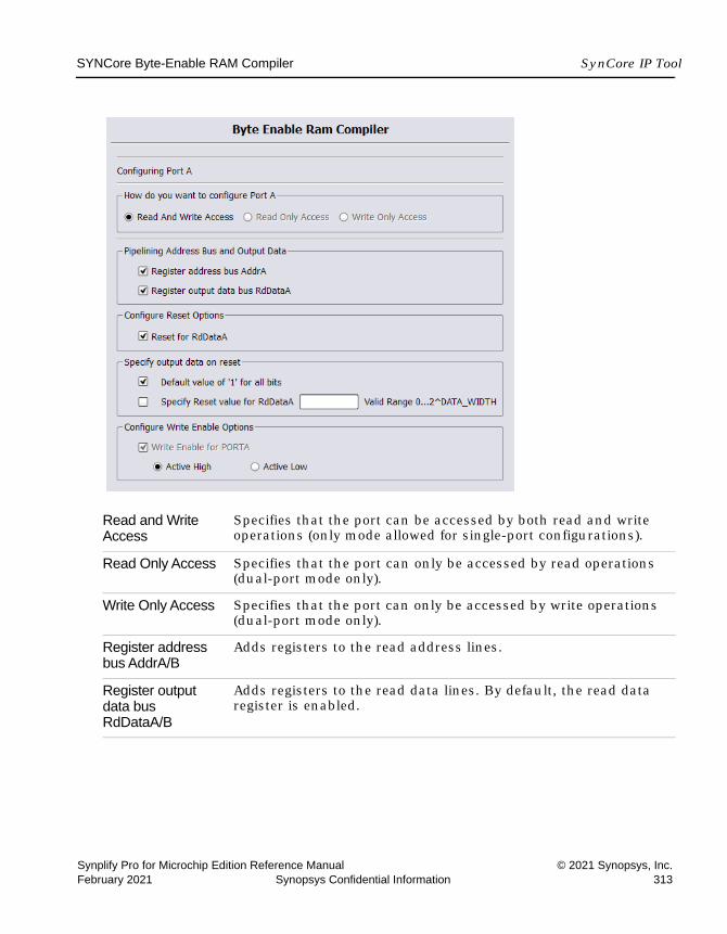
SYNCore Byte-Enable RAM Compiler SynCore IP Tool
Synplify Pro for Microchip Edition Reference Manual © 2021 Synopsys, Inc.February 2021 Synopsys Confidential Information 313
Read and Write Access
Specifies that the port can be accessed by both read and write operations (only mode allowed for single-port configurations).
Read Only Access Specifies that the port can only be accessed by read operations (dual-port mode only).
Write Only Access Specifies that the port can only be accessed by write operations (dual-port mode only).
Register address bus AddrA/B
Adds registers to the read address lines.
Register output data bus RdDataA/B
Adds registers to the read data lines. By default, the read data register is enabled.

LO
SynCore IP Tool SYNCore Byte-Enable RAM Compiler
© 2021 Synopsys, Inc. Synplify Pro for Microchip Edition Reference Manual314 Synopsys Confidential Information February 2021
Read/Write Timing Sequences The waveforms in this section describe the behavior of the byte-enable RAM for both read and write operations.
Read OperationOn each active edge of the clock when there is a change in address, data is valid on the same clock or next clock (depending on latency parameter values for read address and read data ports). Active reset ignores any change in input address, and data and output data are initialized to user-defined values set by parameters RST_RDATA_A and RST_RDATA_B for port A and port B, respectively.
The following waveform shows the read sequence of the byte-enable RAM component with read data registered in single-port mode.
Reset for RdDataA/B
Specifies the reset type for registered read data: • Reset type is synchronous when Reset for RdDataA/B is enabled• Reset type is no reset when Reset for RdDataA/B is disabled
Specify output data on reset
Specifies reset value for registered read data (applies only when RdDataA/B is enabled):• Default value of ‘1’ for all bits - sets read data to all 1’s on reset• Specify Reset value for RdDataA/B - specifies reset value for read
data; when enabled, value is entered in adjacent field
Write Enable for Port A/B
Specifies the write enable level for Port A/B. Default is Active High.
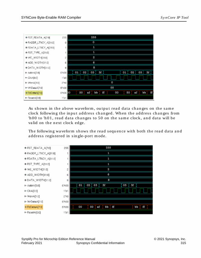
SYNCore Byte-Enable RAM Compiler SynCore IP Tool
Synplify Pro for Microchip Edition Reference Manual © 2021 Synopsys, Inc.February 2021 Synopsys Confidential Information 315
As shown in the above waveform, output read data changes on the same clock following the input address changed. When the address changes from 'h00 to 'h01, read data changes to 50 on the same clock, and data will be valid on the next clock edge.
The following waveform shows the read sequence with both the read data and address registered in single-port mode.

LO
SynCore IP Tool SYNCore Byte-Enable RAM Compiler
© 2021 Synopsys, Inc. Synplify Pro for Microchip Edition Reference Manual316 Synopsys Confidential Information February 2021
As shown in the above waveform, output read data changes on the next clock edge after the input address changes. When the address changes from 'h00 to 'h01, read data changes to 50 on the next clock, and data is valid on the next clock edge.
Note: The read sequence for dual-port mode is the same as single port; read/write conflicts occurring due to accessing the same location from both ports are the user’s responsibility.
Write OperationThe following waveform shows a write sequence with read-after write in single-port mode.
On each active edge of the clock when there is a change in address with an active enable, data is written into memory on the same clock. When enable is not active, any change in address or data is ignored. Active reset ignores any change in input address and data.

SYNCore Byte-Enable RAM Compiler SynCore IP Tool
Synplify Pro for Microchip Edition Reference Manual © 2021 Synopsys, Inc.February 2021 Synopsys Confidential Information 317
The width of the write enable is controlled by the WE_WIDTH parameter. Input data is symmetrically divided and controlled by each write enable. For example, with a data width of 32 and a write enable width of 4, each bit of the write enable controls 8 bits of data (32/4=8). The byte-enable RAM compiler will error for wrong combination data width and write enable values.
The above waveform shows a write sequence with all possible values for write enable followed by a read:
• Value for parameter WE_WIDTH is 2 and DATA_WIDTH is 8 so each write enable controls 4 bits of input data.
• WenA value changes from 1 to 2, 2 to 0, and 0 to 3 which toggles all possible combinations of write enable.
The first sequence of address, write enable changes to perform a write sequence and the data patterns written to memory are 00, aa, ff. The read data pattern reflects the current content of memory before the write.
The second address sequence is a read (WenA is always zero). As shown in the read pattern, only the respective bits of data are written according to the write enable value.
Note: The write sequence for dual-port mode is the same as single port; conflicts occurring due to writing the same location from both ports are the user’s responsibility.
Parameter ListThe following table lists the file entries corresponding to the byte-enable RAM wizard parameters.
Name Description Default Value Range
ADDR_WIDTH Bit/byte enable RAM address width
2 multiples of 2
DATA_WIDTH Data width for input and output data, common to both Port A and Port B
8 2 to 256
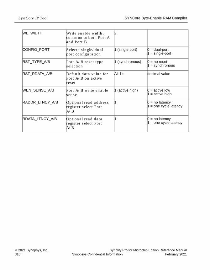
LO
SynCore IP Tool SYNCore Byte-Enable RAM Compiler
© 2021 Synopsys, Inc. Synplify Pro for Microchip Edition Reference Manual318 Synopsys Confidential Information February 2021
WE_WIDTH Write enable width, common to both Port A and Port B
2
CONFIG_PORT Selects single/dual port configuration
1 (single port) 0 = dual-port1 = single-port
RST_TYPE_A/B Port A/B reset type selection
1 (synchronous) 0 = no reset1 = synchronous
RST_RDATA_A/B Default data value for Port A/B on active reset
All 1’s decimal value
WEN_SENSE_A/B Port A/B write enable sense
1 (active high) 0 = active low1 = active high
RADDR_LTNCY_A/B Optional read address register select Port A/B
1 0 = no latency1 = one cycle latency
RDATA_LTNCY_A/B Optional read data register select Port A/B
1 0 = no latency1 = one cycle latency

SYNCore ROM Compiler SynCore IP Tool
Synplify Pro for Microchip Edition Reference Manual © 2021 Synopsys, Inc.February 2021 Synopsys Confidential Information 319
SYNCore ROM Compiler The SYNCore ROM Compiler generates Verilog code for your ROM implemen-tation. This section describes the following:
• Functional Overview, on page 319
• Specifying ROMs with SYNCore, on page 321
• SYNCore ROM Wizard, on page 326
• Single-Port Read Operation, on page 330
• Dual-Port Read Operation, on page 331
• Parameter List, on page 331
Functional OverviewThe SYNCore ROM component supports ROM implementations using block ROM or logic memory. For each configuration, design optimizations are made for optimum usage of core resources. Both single- and dual-port memory configurations are supported. Single-port ROM allows read access to memory through a single port, and dual-port ROM allows read access to memory through two ports. The following figure illustrates the supported signals for both configurations.

LO
SynCore IP Tool SYNCore ROM Compiler
© 2021 Synopsys, Inc. Synplify Pro for Microchip Edition Reference Manual320 Synopsys Confidential Information February 2021
In the single-port (Port A) configuration, signals are synchronized to ClkA; ResetA can be synchronous or asynchronous depending on parameter selec-tion. The read address (AddrA) and/or data output (DataA) can be registered to increase memory performance and improve timing. In the dual-port configu-ration, all Port A signals are synchronized to ClkA, and all PortB signals are synchronized to ClkB. ResetA and ResetB can be synchronous or asynchronous depending on parameter selection, and both data outputs can be registered and are subject to the same clock latencies. Registering the data output is recommended.
Note: When the data output is unregistered, the data is immediately set to its predefined reset value concurrent with an active reset signal.
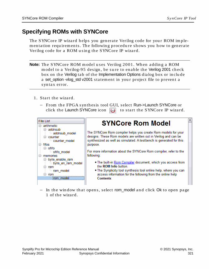
SYNCore ROM Compiler SynCore IP Tool
Synplify Pro for Microchip Edition Reference Manual © 2021 Synopsys, Inc.February 2021 Synopsys Confidential Information 321
Specifying ROMs with SYNCore The SYNCore IP wizard helps you generate Verilog code for your ROM imple-mentation requirements. The following procedure shows you how to generate Verilog code for a ROM using the SYNCore IP wizard.
Note: The SYNCore ROM model uses Verilog 2001. When adding a ROM model to a Verilog-95 design, be sure to enable the Verilog 2001 check box on the Verilog tab of the Implementation Options dialog box or include a set_option -vlog_std v2001 statement in your project file to prevent a syntax error.
1. Start the wizard.
– From the FPGA synthesis tool GUI, select Run->Launch SYNCore or click the Launch SYNCore icon to start the SYNCore IP wizard.
– In the window that opens, select rom_model and click Ok to open page 1 of the wizard.

LO
SynCore IP Tool SYNCore ROM Compiler
© 2021 Synopsys, Inc. Synplify Pro for Microchip Edition Reference Manual322 Synopsys Confidential Information February 2021
2. Specify the parameters you need in the wizard. For details about the parameters, see Specifying ROM Parameters, on page 325. The ROM symbol on the left reflects any parameters you set.
3. After you have specified all the parameters you need, click the Generate button in the lower left corner. The tool displays a confirmation message (TCL execution successful!) and writes the required files to the directory you specified on page 1 of the wizard. The HDL code is in Verilog.
SYNCore also generates a testbench for the ROM. The testbench covers a limited set of vectors.
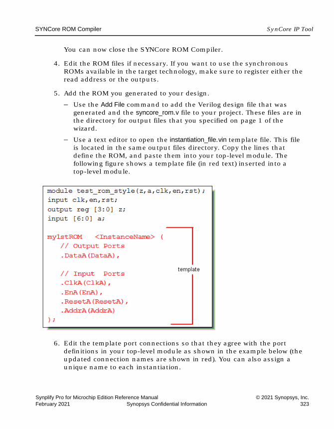
SYNCore ROM Compiler SynCore IP Tool
Synplify Pro for Microchip Edition Reference Manual © 2021 Synopsys, Inc.February 2021 Synopsys Confidential Information 323
You can now close the SYNCore ROM Compiler.
4. Edit the ROM files if necessary. If you want to use the synchronous ROMs available in the target technology, make sure to register either the read address or the outputs.
5. Add the ROM you generated to your design.
– Use the Add File command to add the Verilog design file that was generated and the syncore_rom.v file to your project. These files are in the directory for output files that you specified on page 1 of the wizard.
– Use a text editor to open the instantiation_file.vin template file. This file is located in the same output files directory. Copy the lines that define the ROM, and paste them into your top-level module. The following figure shows a template file (in red text) inserted into a top-level module.
6. Edit the template port connections so that they agree with the port definitions in your top-level module as shown in the example below (the updated connection names are shown in red). You can also assign a unique name to each instantiation.

LO
SynCore IP Tool SYNCore ROM Compiler
© 2021 Synopsys, Inc. Synplify Pro for Microchip Edition Reference Manual324 Synopsys Confidential Information February 2021
Port List PortA interface signals are applicable for both single-port and dual-port configurations; PortB signals are applicable for dual-port configuration only.
Name Type Description
ClkA Input Clock input for Port A
EnA Input Enable input for Port A
AddrA Input Read address for Port A
ResetA Input Reset or interface disable pin for Port A
DataA Output Read data output for Port A
ClkB Input Clock input for Port B
EnB Input Enable input for Port B
AddrB Input Read address for Port B
ResetB Input Reset or interface disable pin for Port B
DataB Output Read data output for Port B
module test_rom_style(z,a,clk,en,rst);input clk,en,rst;output reg [3:0] z;input [6:0] a;
my1stROM decode_rom( // Output Ports .DataA(z),
// Input Ports .ClkA(clk), .EnA(en), .ResetA(rst), .AddrA(a));

SYNCore ROM Compiler SynCore IP Tool
Synplify Pro for Microchip Edition Reference Manual © 2021 Synopsys, Inc.February 2021 Synopsys Confidential Information 325
Specifying ROM ParametersIf you are creating a single-port ROM with the SYNCore IP wizard, you need to specify a single read address and a single clock, and you only need to configure the Port A parameters on page 2. If you are creating a dual-port ROM, you must additionally configure the Port B parameters on page 3. The following procedure lists what you need to specify. For descriptions of each parameter, refer to SYNCore RAM Wizard, on page 289.
1. Start the SYNCore ROM wizard, as described in Specifying ROMs with SYNCore, on page 321.
2. Do the following on page 1 of the ROM wizard:
– In Component Name, specify a name for the memory. Do not use spaces.
– In Directory, specify a directory where you want the output files to be written. Do not use spaces.
– In Filename, specify a name for the Verilog file that will be generated with the ROM specifications. Do not use spaces.
– Enter values for Read Data width and ROM address width (minimum depth value is 2; maximum depth of the memory is limited to 2^256).
– Select Single Port Rom to indicate that you want to generate a single-port ROM or select Dual Port Rom to generate a dual-port ROM.
– Click Next. The wizard opens page 2 where you set parameters for Port A.
The ROM symbol dynamically updates to reflect any parameters you set.
3. Do the following on page 2 (Configuring Port A) of the RAM wizard:
– For synchronous ROMs, select Register address bus AddrA and/or Register output data bus DataA to register the read address and/or the outputs. Selecting either checkbox enables the Enable for Port A checkbox which is used to select the Enable level.
– Set the Configure Reset Options. Enabling the checkbox enables the type of reset (asynchronous or synchronous) and allows an output data pattern (all 1’s or a specified pattern) to be defined on page 4.
4. If you are generating a dual-port ROM, set the port B parameters on page 3 (the page 3 parameters are only enabled when Dual Port Rom is selected on page 1).
LO
SynCore IP Tool SYNCore ROM Compiler
© 2021 Synopsys, Inc. Synplify Pro for Microchip Edition Reference Manual326 Synopsys Confidential Information February 2021
5. On page 4, specify the location of the ROM initialization file and the data format (Hexadecimal or Binary). ROM initialization is supported using memory-coefficient files. The data format is either binary or hexadecimal with each data entry on a new line in the memory-coefficient file (specified by parameter INIT_FILE). Supported file types are txt, mem, dat, and init (recommended).
6. Generate the ROM by clicking Generate, as described in Specifying ROMs with SYNCore, on page 321 and add it to your design. All output files are in the directory you specified on page 1 of the wizard.
For read/write timing diagrams, see Read/Write Timing Sequences, on page 299.
SYNCore ROM WizardThe following describe the parameters you can set in the ROM wizard, which opens when you select rom_model:
• SYNCore ROM Parameters Page 1, on page 327
• SYNCore ROM Parameters Pages 2 and 3, on page 328
• SYNCore ROM Parameters Page 4, on page 330

SYNCore ROM Compiler SynCore IP Tool
Synplify Pro for Microchip Edition Reference Manual © 2021 Synopsys, Inc.February 2021 Synopsys Confidential Information 327
SYNCore ROM Parameters Page 1
Component Name Specifies the name of the component. This is the name that you instantiate in your design file to create an instance of the SYNCore ROM in your design. Do not use spaces.
Directory Specifies the directory where the generated files are stored. Do not use spaces. The following files are created:filelist.txt - lists files written out by SYNCoreoptions.txt - lists the options selected in SYNCorereadme.txt - contains a brief description and known issuessyncore_rom.v - Verilog library file required to generate ROM modeltestbench.v - Verilog testbench file for testing the ROM model instantiation_file.vin - describes how to instantiate the wrapper filecomponent.v - ROM model wrapper file generated by SYNCoreNote that running the ROM wizard in the same directory overwrites the existing files.
File Name Specifies the name of the generated file containing the HDL description of the compiled ROM. Do not use spaces.

LO
SynCore IP Tool SYNCore ROM Compiler
© 2021 Synopsys, Inc. Synplify Pro for Microchip Edition Reference Manual328 Synopsys Confidential Information February 2021
SYNCore ROM Parameters Pages 2 and 3The port implementation parameters on pages 2 and 3 are the same; page 2 applies to Port A (single- and dual-port configurations), and page 3 applies to Port B (dual-port configurations only).
Read Data Width Specifies the read data width of the ROM. The unit used is the number of bits and ranges from 2 to 256. Default value is 8. The read data width is common to both Port A and Port B. The corresponding file parameter is DATA_WIDTH=n.
ROM address width Specifies the address depth for the memory. The unit used is the number of bits. Default value is 10. The corresponding file parameter is ADD_WIDTH=n.
Single Port Rom When enabled, generates a single-port ROM. The corresponding file parameter is CONFIG_PORT="single".
Dual Port Rom When enabled, generates a dual-port ROM. The corresponding file parameter is CONFIG_PORT="dual".
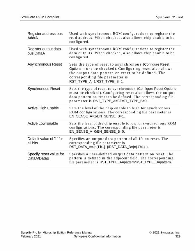
SYNCore ROM Compiler SynCore IP Tool
Synplify Pro for Microchip Edition Reference Manual © 2021 Synopsys, Inc.February 2021 Synopsys Confidential Information 329
Register address bus AddrA
Used with synchronous ROM configurations to register the read address. When checked, also allows chip enable to be configured.
Register output data bus DataA
Used with synchronous ROM configurations to register the data outputs. When checked, also allows chip enable to be configured.
Asynchronous Reset Sets the type of reset to asynchronous (Configure Reset Options must be checked). Configuring reset also allows the output data pattern on reset to be defined. The corresponding file parameter is RST_TYPE_A=1/RST_TYPE_B=1.
Synchronous Reset Sets the type of reset to synchronous (Configure Reset Options must be checked). Configuring reset also allows the output data pattern on reset to be defined. The corresponding file parameter is RST_TYPE_A=0/RST_TYPE_B=0.
Active High Enable Sets the level of the chip enable to high for synchronous ROM configurations. The corresponding file parameter is EN_SENSE_A=1/EN_SENSE_B=1.
Active Low Enable Sets the level of the chip enable to low for synchronous ROM configurations. The corresponding file parameter is EN_SENSE_A=0/EN_SENSE_B=0.
Default value of '1' for all bits
Specifies an output data pattern of all 1’s on reset. The corresponding file parameter is RST_DATA_A={n{1'b1} }/RST_DATA_B={n{1'b1} }.
Specify reset value for DataA/DataB
Specifies a user-defined output data pattern on reset. The pattern is defined in the adjacent field. The corresponding file parameter is RST_TYPE_A=pattern/RST_TYPE_B=pattern.

LO
SynCore IP Tool SYNCore ROM Compiler
© 2021 Synopsys, Inc. Synplify Pro for Microchip Edition Reference Manual330 Synopsys Confidential Information February 2021
SYNCore ROM Parameters Page 4
Single-Port Read OperationFor single-port ROM, it is only necessary to configure Port A (see Specifying ROMs with SYNCore, on page 321. The following diagram shows the read timing for a single-port ROM.
On every active edge of the clock when there is a change in address with an active enable, data will be valid on the same clock or next clock (depending on latency parameter values). When enable is inactive, any address change is ignored, and the data port maintains the last active read value. An active reset ignores any change in input address and forces the output data to its predefined initialization value. The following waveform shows the functional behavior of control signals in single-port mode.
Binary Specifies binary-formatted initialization file.
Hexadecimal Specifies hexadecimal-formatted initial file.
Initialization File Specifies path and filename of initialization file. The corresponding file parameter is INIT_FILE="filename".
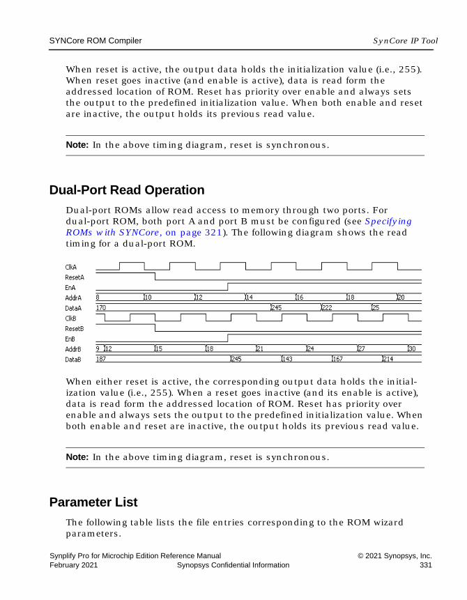
SYNCore ROM Compiler SynCore IP Tool
Synplify Pro for Microchip Edition Reference Manual © 2021 Synopsys, Inc.February 2021 Synopsys Confidential Information 331
When reset is active, the output data holds the initialization value (i.e., 255). When reset goes inactive (and enable is active), data is read form the addressed location of ROM. Reset has priority over enable and always sets the output to the predefined initialization value. When both enable and reset are inactive, the output holds its previous read value.
Note: In the above timing diagram, reset is synchronous.
Dual-Port Read OperationDual-port ROMs allow read access to memory through two ports. For dual-port ROM, both port A and port B must be configured (see Specifying ROMs with SYNCore, on page 321). The following diagram shows the read timing for a dual-port ROM.
When either reset is active, the corresponding output data holds the initial-ization value (i.e., 255). When a reset goes inactive (and its enable is active), data is read form the addressed location of ROM. Reset has priority over enable and always sets the output to the predefined initialization value. When both enable and reset are inactive, the output holds its previous read value.
Note: In the above timing diagram, reset is synchronous.
Parameter ListThe following table lists the file entries corresponding to the ROM wizard parameters.
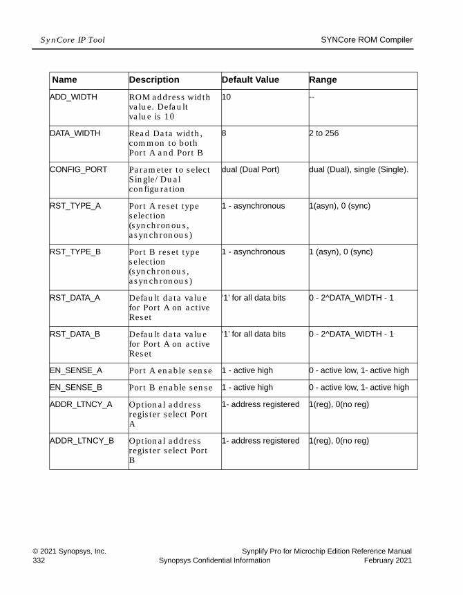
LO
SynCore IP Tool SYNCore ROM Compiler
© 2021 Synopsys, Inc. Synplify Pro for Microchip Edition Reference Manual332 Synopsys Confidential Information February 2021
Name Description Default Value Range
ADD_WIDTH ROM address width value. Default value is 10
10 --
DATA_WIDTH Read Data width, common to both Port A and Port B
8 2 to 256
CONFIG_PORT Parameter to select Single/Dual configuration
dual (Dual Port) dual (Dual), single (Single).
RST_TYPE_A Port A reset type selection (synchronous, asynchronous)
1 - asynchronous 1(asyn), 0 (sync)
RST_TYPE_B Port B reset type selection (synchronous, asynchronous)
1 - asynchronous 1 (asyn), 0 (sync)
RST_DATA_A Default data value for Port A on active Reset
‘1’ for all data bits 0 - 2^DATA_WIDTH - 1
RST_DATA_B Default data value for Port A on active Reset
‘1’ for all data bits 0 - 2^DATA_WIDTH - 1
EN_SENSE_A Port A enable sense 1 - active high 0 - active low, 1- active high
EN_SENSE_B Port B enable sense 1 - active high 0 - active low, 1- active high
ADDR_LTNCY_A Optional address register select Port A
1- address registered 1(reg), 0(no reg)
ADDR_LTNCY_B Optional address register select Port B
1- address registered 1(reg), 0(no reg)

SYNCore ROM Compiler SynCore IP Tool
Synplify Pro for Microchip Edition Reference Manual © 2021 Synopsys, Inc.February 2021 Synopsys Confidential Information 333
DATA_LTNCY_A Optional data register select Port A
1- data registered 1(reg), 0(no reg)
DATA_LTNCY_B Optional data register select Port B
1- data registered 1(reg), 0(no reg)
INIT_FILE Initial values file name
init.txt --
LO
SynCore IP Tool SYNCore Adder/Subtractor Compiler
© 2021 Synopsys, Inc. Synplify Pro for Microchip Edition Reference Manual334 Synopsys Confidential Information February 2021
SYNCore Adder/Subtractor Compiler The SYNCore adder/subtractor compiler generates Verilog code for a parame-trizable, pipelined adder/subtractor. This section describes the functionality of this block in detail.
• Functional Description, on page 334
• Specifying Adder/Subtractors with SYNCore, on page 335
• SYNCore Adder/Subtractor Wizard, on page 343
• Adder, on page 346
• Subtractor, on page 349
• Dynamic Adder/Subtractor, on page 352
Functional DescriptionThe adder/subtractor has a single clock that controls the entire pipeline stages (if used) of the adder/subtractor.
As its name implies, this block just adds/subtracts the inputs and provides the output result. One of the inputs can be configured as a constant. The data inputs and outputs of the adder/subtractor can be pipelined; the pipeline stages can be 0 or 1, and can be configured individually. The individual pipeline stage registers include their own reset and enable ports.
The reset to all of the pipeline registers can be configured either as synchro-nous or asynchronous using the RESET_TYPE parameter. The reset type of the pipeline registers cannot be configured individually.

SYNCore Adder/Subtractor Compiler SynCore IP Tool
Synplify Pro for Microchip Edition Reference Manual © 2021 Synopsys, Inc.February 2021 Synopsys Confidential Information 335
SYNCore adder/subtractor has ADD_N_SUB parameter, which can take three values ADD, SUB, or DYNAMIC. Based on this parameter value, the adder/subtractor can be configured as follows.
• Adder
• Subtractor
• Dynamic Adder and Subtractor
Specifying Adder/Subtractors with SYNCore The SYNCore IP wizard helps you generate Verilog code for your adder/subtractor implementation requirements. The following procedure shows you how to generate Verilog code for an adder/subtractor using the SYNCore IP wizard.
Note: The SYNCore adder/subtractor models use Verilog 2001. When adding an adder/subtractor model to a Verilog-95 design, be sure to enable the Verilog 2001 check box on the Verilog tab of the Implementation Options dialog box or include a set_option -vlog_std v2001 statement in your project file to prevent a syntax error.
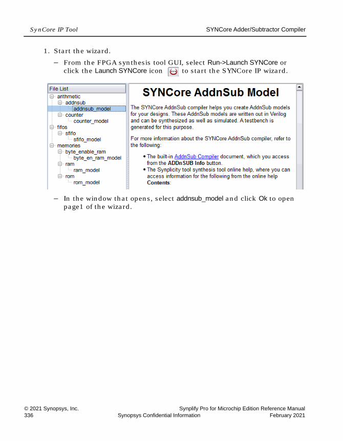
LO
SynCore IP Tool SYNCore Adder/Subtractor Compiler
© 2021 Synopsys, Inc. Synplify Pro for Microchip Edition Reference Manual336 Synopsys Confidential Information February 2021
1. Start the wizard.
– From the FPGA synthesis tool GUI, select Run->Launch SYNCore or click the Launch SYNCore icon to start the SYNCore IP wizard.
– Ιn the window that opens, select addnsub_model and click Ok to open page1 of the wizard.
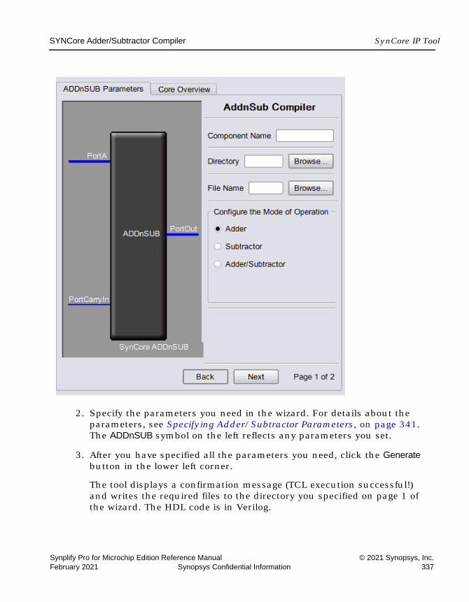
SYNCore Adder/Subtractor Compiler SynCore IP Tool
Synplify Pro for Microchip Edition Reference Manual © 2021 Synopsys, Inc.February 2021 Synopsys Confidential Information 337
2. Specify the parameters you need in the wizard. For details about the parameters, see Specifying Adder/Subtractor Parameters, on page 341. The ADDnSUB symbol on the left reflects any parameters you set.
3. After you have specified all the parameters you need, click the Generate button in the lower left corner.
The tool displays a confirmation message (TCL execution successful!) and writes the required files to the directory you specified on page 1 of the wizard. The HDL code is in Verilog.

LO
SynCore IP Tool SYNCore Adder/Subtractor Compiler
© 2021 Synopsys, Inc. Synplify Pro for Microchip Edition Reference Manual338 Synopsys Confidential Information February 2021
The SYNCore wizard also generates a testbench for your adder/subtractor. The testbench covers a limited set of vectors. You can now close the wizard.
4. Add the adder/subtractor you generated to your design.
– Edit the adder/subtractor files if necessary.
– Use the Add File command to add the Verilog design file that was generated and the syncore_addnsub.v file to your project. These files are in the directory for output files that you specified on page 1 of the wizard.
– Use a text editor to open the instantiation_file.v template file. This file is located in the same output files directory. Copy the lines that define the adder/subtractor and paste them into your top-level module. The following figure shows a template file (in red text) inserted into a top-level module.
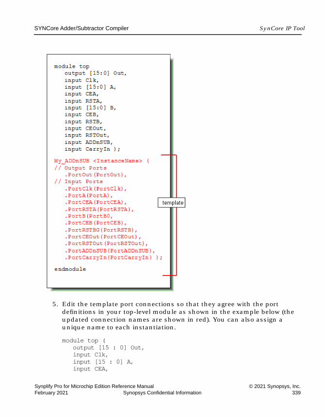
SYNCore Adder/Subtractor Compiler SynCore IP Tool
Synplify Pro for Microchip Edition Reference Manual © 2021 Synopsys, Inc.February 2021 Synopsys Confidential Information 339
5. Edit the template port connections so that they agree with the port definitions in your top-level module as shown in the example below (the updated connection names are shown in red). You can also assign a unique name to each instantiation.
module top (output [15 : 0] Out, input Clk,input [15 : 0] A,input CEA,
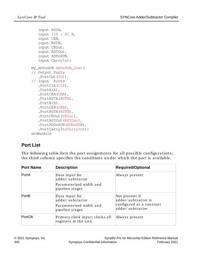
LO
SynCore IP Tool SYNCore Adder/Subtractor Compiler
© 2021 Synopsys, Inc. Synplify Pro for Microchip Edition Reference Manual340 Synopsys Confidential Information February 2021
input RSTA,input [15 : 0] B,input CEB,input RSTB,input CEOut, input RSTOut, input ADDnSUB,input CarryIn);
My_ADDnSUB ADDnSUB_inst(// Output Ports
.PortOut(Out), // Input Ports
.PortClk(Clk),
.PortA(A),
.PortCEA(CEA),
.PortRSTA(RSTA),
.PortB(B),
.PortCEB(CEB),
.PortRSTB(RSTB),
.PortCEOut(CEOut),
.PortRSTOut(RSTOut),
.PortADDnSUB(ADDnSUB),
.PortCarryIn(CarryIn));endmodule
Port ListThe following table lists the port assignments for all possible configurations; the third column specifies the conditions under which the port is available.
Port Name Description Required/Optional
PortA Data input for adder/subtractorParameterized width and pipeline stages
Always present
PortB Data input for adder/subtractor Parameterized width and pipeline stages
Not present if adder/subtractor is configured as a constant adder/subtractor
PortClk Primary clock input; clocks all registers in the unit
Always present
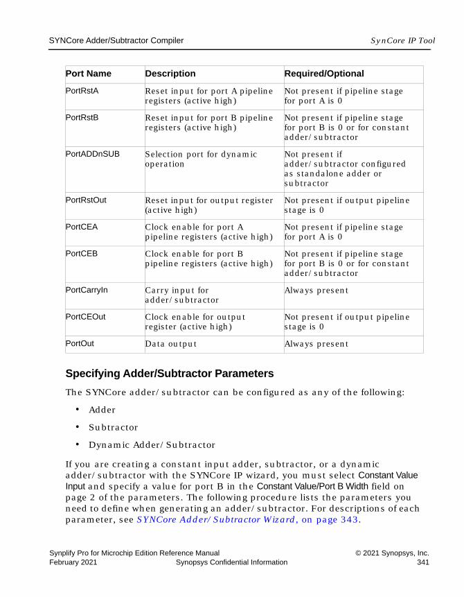
SYNCore Adder/Subtractor Compiler SynCore IP Tool
Synplify Pro for Microchip Edition Reference Manual © 2021 Synopsys, Inc.February 2021 Synopsys Confidential Information 341
Specifying Adder/Subtractor ParametersThe SYNCore adder/subtractor can be configured as any of the following:
• Adder
• Subtractor
• Dynamic Adder/Subtractor
If you are creating a constant input adder, subtractor, or a dynamic adder/subtractor with the SYNCore IP wizard, you must select Constant Value Input and specify a value for port B in the Constant Value/Port B Width field on page 2 of the parameters. The following procedure lists the parameters you need to define when generating an adder/subtractor. For descriptions of each parameter, see SYNCore Adder/Subtractor Wizard, on page 343.
PortRstA Reset input for port A pipeline registers (active high)
Not present if pipeline stage for port A is 0
PortRstB Reset input for port B pipeline registers (active high)
Not present if pipeline stage for port B is 0 or for constant adder/subtractor
PortADDnSUB Selection port for dynamic operation
Not present if adder/subtractor configured as standalone adder or subtractor
PortRstOut Reset input for output register (active high)
Not present if output pipeline stage is 0
PortCEA Clock enable for port A pipeline registers (active high)
Not present if pipeline stage for port A is 0
PortCEB Clock enable for port B pipeline registers (active high)
Not present if pipeline stage for port B is 0 or for constant adder/subtractor
PortCarryIn Carry input for adder/subtractor
Always present
PortCEOut Clock enable for output register (active high)
Not present if output pipeline stage is 0
PortOut Data output Always present
Port Name Description Required/Optional

LO
SynCore IP Tool SYNCore Adder/Subtractor Compiler
© 2021 Synopsys, Inc. Synplify Pro for Microchip Edition Reference Manual342 Synopsys Confidential Information February 2021
1. Start the SYNCore adder/subtractor wizard as described in Specifying Adder/Subtractors with SYNCore, on page 335.
2. Enter the following on page 1 of the wizard:
– Ιn the Component Name field, specify a name for your adder/subtractor. Do not use spaces.
– In the Directory field, specify a directory where you want the output files to be written. Do not use spaces.
– Ιn the Filename field, specify a name for the Verilog file that will be generated with the adder/subtractor definitions. Do not use spaces.
– Select the appropriate configuration in Configure the Mode of Operation.
3. Click Next. The wizard opens page 2 where you set parameters for port A and port B.
4. Configure Port A and B.
– In the Configure Port A section, enter a value in the Port A Width field.
– If you are defining a synchronous adder/subtractor, check Register Input A and then check Clock Enable for Register A and/or Reset for Register A.
– To configure port B as a constant port, go to the Configure Port B section and check Constant Value Input. Enter the constant value in the Constant Value/Port B Width field.
– To configure port B as a dynamic port, go to the Configure Port B section and check Enable Port B and enter the port width in the Constant Value/Port B Width field.
– To define a synchronous adder/subtractor, check Register Input B and then check Clock Enable for Register B and/or Reset for Register B.
5. In the Configure Output Port section:
– Enter a value in the Output port Width field.
– If you are registering the output port, check Register output Port.
– If you are defining a synchronous adder/subtractor check Clock Enable for Register PortOut and/or Reset for Register PortOut.
6. In the Configure Reset type for all Reset Signal section, click Synchronous Reset or Asynchronous Reset as appropriate.

SYNCore Adder/Subtractor Compiler SynCore IP Tool
Synplify Pro for Microchip Edition Reference Manual © 2021 Synopsys, Inc.February 2021 Synopsys Confidential Information 343
As you enter the page 2 parameters, the ADDnSUB symbol dynamically updates to reflect the parameters you set.
7. Generate the adder/subtractor by clicking the Generate button as described in Specifying Adder/Subtractors with SYNCore, on page 335 and add it to your design. All output files are in the directory you specified on page 1 of the wizard.
SYNCore Adder/Subtractor WizardThe following describe the parameters you can set in the adder/subtractor wizard, which opens when you select addnsub_model:
• SYNCore Adder/Subtractor Parameters Page 1, on page 343
• SYNCore Adder/Subtractor Parameters Page 2, on page 345
SYNCore Adder/Subtractor Parameters Page 1

LO
SynCore IP Tool SYNCore Adder/Subtractor Compiler
© 2021 Synopsys, Inc. Synplify Pro for Microchip Edition Reference Manual344 Synopsys Confidential Information February 2021
Component Name Specifies a name for the adder/subtractor. This is the name that you instantiate in your design file to create an instance of the SYNCore adder/subtractor in your design. Do not use spaces.
Directory Indicates the directory where the generated files will be stored. Do not use spaces. The following files are created:• filelist.txt - lists files written out by SYNCore• options.txt - lists the options selected in SYNCore• readme.txt - contains a brief description and known issues• syncore_ADDnSUB.v - Verilog library file required to
generate adder/subtractor model• testbench.v - Verilog testbench file for testing the
adder/subtractor model• instantiation_file.vin - describes how to instantiate the
wrapper file• component.v - adder/subtractor model wrapper file
generated by SYNCoreNote that running the wizard in the same directory overwrites any existing files.
Filename Specifies the name of the generated file containing the HDL description of the generated adder/subtractor. Do not use spaces.
Adder When enabled, generates an adder (the corresponding file parameter is ADD_N_SUB ="ADD").
Subtractor When enabled, generates a subtractor (the corresponding file parameter is ADD_N_SUB ="SUB").
Adder/Subtractor When enabled, generates a dynamic adder/subtractor (the corresponding file parameter is ADD_N_SUB ="DYNAMIC").
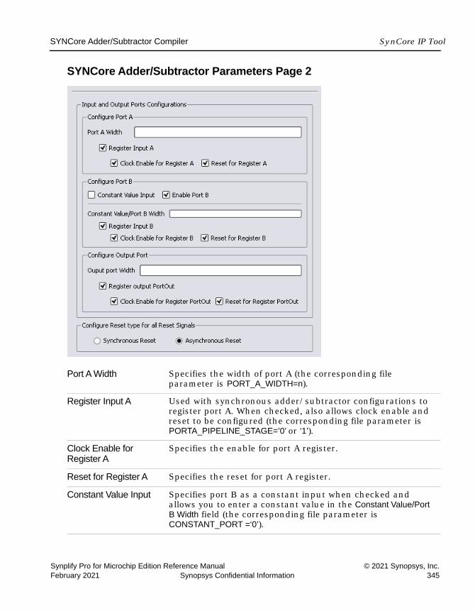
SYNCore Adder/Subtractor Compiler SynCore IP Tool
Synplify Pro for Microchip Edition Reference Manual © 2021 Synopsys, Inc.February 2021 Synopsys Confidential Information 345
SYNCore Adder/Subtractor Parameters Page 2
Port A Width Specifies the width of port A (the corresponding file parameter is PORT_A_WIDTH=n).
Register Input A Used with synchronous adder/subtractor configurations to register port A. When checked, also allows clock enable and reset to be configured (the corresponding file parameter is PORTA_PIPELINE_STAGE=’0’ or ‘1’).
Clock Enable for Register A
Specifies the enable for port A register.
Reset for Register A Specifies the reset for port A register.
Constant Value Input Specifies port B as a constant input when checked and allows you to enter a constant value in the Constant Value/Port B Width field (the corresponding file parameter is CONSTANT_PORT =‘0’).

LO
SynCore IP Tool SYNCore Adder/Subtractor Compiler
© 2021 Synopsys, Inc. Synplify Pro for Microchip Edition Reference Manual346 Synopsys Confidential Information February 2021
AdderBased on the parameter CONSTANT_PORT, the adder can be configured in two ways.
• CONSTANT_PORT='0' - adder with two input ports (port A and port B)
• CONSTANT_PORT='1' - adder with one constant port
Enable Port B Specifies port B as an input when checked and allows you to enter a port B width in the Constant Value/Port B Width field (the corresponding file parameter is CONSTANT_PORT =‘1’).
Constant Value/Port B Width
Specifies either a constant value or port B width depending on Constant Value Input and Enable Port B selection (the corresponding file parameters are CONSTANT_VALUE= n or PORT_B_WIDTH=n).
Register Input B Used with synchronous adder/subtractor configurations to register port B. When checked, also allows clock enable and reset to be configured (the corresponding file parameter is PORTB_PIPELINE_STAGE=’0’ or ‘1’).
Clock Enable for Register B
Specifies the enable for the port B register.
Reset for Register B Specifies the reset for the port B register.
Output port Width Specifies the width of the output port (the corresponding file parameter is PORT_OUT_WIDTH=n).
Register output PortOut
Used with synchronous adder/subtractor configurations to register the output port. When checked, also allows clock enable and reset to be configured (the corresponding file parameter is PORTOUT_PIPELINE_STAGE=’0’ or ‘1’.
Clock Enable for Register PortOut
Specifies the enable for the output port register.
Reset for Register PortOut
Specifies the reset for the output port register.
Synchronous Reset Sets the type of reset to synchronous (the corresponding file parameter is RESET_TYPE=’0’).
Asynchronous Reset Sets the type of reset to asynchronous (the corresponding file parameter is RESET_TYPE=’1’).
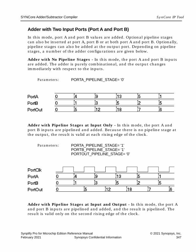
SYNCore Adder/Subtractor Compiler SynCore IP Tool
Synplify Pro for Microchip Edition Reference Manual © 2021 Synopsys, Inc.February 2021 Synopsys Confidential Information 347
Adder with Two Input Ports (Port A and Port B)In this mode, port A and port B values are added. Optional pipeline stages can also be inserted at port A, port B or at both port A and port B. Optionally, pipeline stages can also be added at the output port. Depending on pipeline stages, a number of the adder configurations are given below.
Adder with No Pipeline Stages - In this mode, the port A and port B inputs are added. The adder is purely combinational, and the output changes immediately with respect to the inputs.
Adder with Pipeline Stages at Input Only - In this mode, the port A and port B inputs are pipelined and added. Because there is no pipeline stage at the output, the result is valid at each rising edge of the clock.
Adder with Pipeline Stages at Input and Output - In this mode, the port A and port B inputs are pipelined and added, and the result is pipelined. The result is valid only on the second rising edge of the clock.
Parameters: PORTA_PIPELINE_STAGE= ‘0’
Parameters: PORTA_PIPELINE_STAGE= ‘1’PORTB_PIPELINE_STAGE= ‘1’PORTOUT_PIPELINE_STAGE= ‘0’
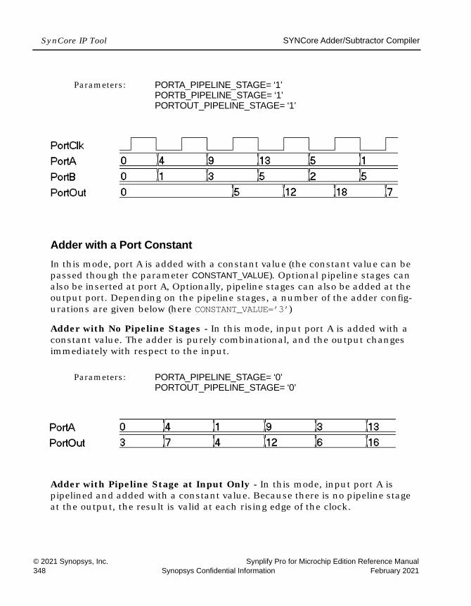
LO
SynCore IP Tool SYNCore Adder/Subtractor Compiler
© 2021 Synopsys, Inc. Synplify Pro for Microchip Edition Reference Manual348 Synopsys Confidential Information February 2021
Adder with a Port ConstantIn this mode, port A is added with a constant value (the constant value can be passed though the parameter CONSTANT_VALUE). Optional pipeline stages can also be inserted at port A, Optionally, pipeline stages can also be added at the output port. Depending on the pipeline stages, a number of the adder config-urations are given below (here CONSTANT_VALUE=’3’)Adder with No Pipeline Stages - In this mode, input port A is added with a constant value. The adder is purely combinational, and the output changes immediately with respect to the input.
Adder with Pipeline Stage at Input Only - In this mode, input port A is pipelined and added with a constant value. Because there is no pipeline stage at the output, the result is valid at each rising edge of the clock.
Parameters: PORTA_PIPELINE_STAGE= ‘1’PORTB_PIPELINE_STAGE= ‘1’PORTOUT_PIPELINE_STAGE= ‘1’
Parameters: PORTA_PIPELINE_STAGE= ‘0’PORTOUT_PIPELINE_STAGE= ‘0’
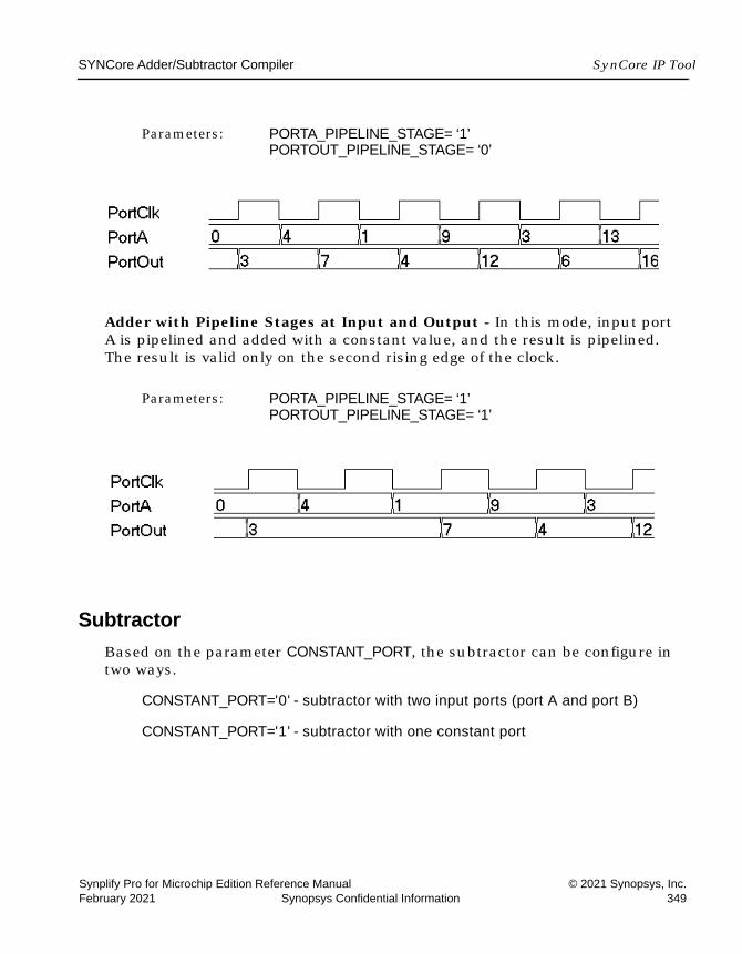
SYNCore Adder/Subtractor Compiler SynCore IP Tool
Synplify Pro for Microchip Edition Reference Manual © 2021 Synopsys, Inc.February 2021 Synopsys Confidential Information 349
Adder with Pipeline Stages at Input and Output - In this mode, input port A is pipelined and added with a constant value, and the result is pipelined. The result is valid only on the second rising edge of the clock.
SubtractorBased on the parameter CONSTANT_PORT, the subtractor can be configure in two ways.
CONSTANT_PORT='0' - subtractor with two input ports (port A and port B)
CONSTANT_PORT='1' - subtractor with one constant port
Parameters: PORTA_PIPELINE_STAGE= ‘1’PORTOUT_PIPELINE_STAGE= ‘0’
Parameters: PORTA_PIPELINE_STAGE= ‘1’PORTOUT_PIPELINE_STAGE= ‘1’

LO
SynCore IP Tool SYNCore Adder/Subtractor Compiler
© 2021 Synopsys, Inc. Synplify Pro for Microchip Edition Reference Manual350 Synopsys Confidential Information February 2021
Subtractor with Two Input Ports (Port A and Port B)In this mode, port B is subtracted from port A. Optional pipeline stages can also be inserted at port A, port B, or both ports. Optionally, pipeline stages can also be added at the output port. Depending on the pipeline stages, a number of the subtractor configurations are given below.
Subtractor with No Pipeline Stages - In this mode, input port B is subtracted from port A, and the subtractor is purely combinational. The output changes immediately with respect to the inputs.
Subtractor with Pipeline Stages at Input Only - In this mode, input port B and input PortA are pipelined and then subtracted. Because there is no pipeline stage at the output, the result is valid at each rising edge of the clock.
Parameters: PORTA_PIPELINE_STAGE= ‘0’PORTB_PIPELINE_STAGE= ‘0’PORTOUT_PIPELINE_STAGE= ‘0’
Parameters: PORTA_PIPELINE_STAGE= ‘1’PORTB_PIPELINE_STAGE= ‘1’PORTOUT_PIPELINE_STAGE= ‘0’
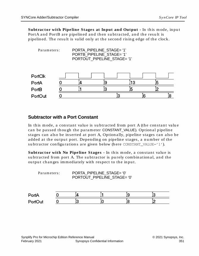
SYNCore Adder/Subtractor Compiler SynCore IP Tool
Synplify Pro for Microchip Edition Reference Manual © 2021 Synopsys, Inc.February 2021 Synopsys Confidential Information 351
Subtractor with Pipeline Stages at Input and Output - In this mode, input PortA and PortB are pipelined and then subtracted, and the result is pipelined. The result is valid only at the second rising edge of the clock.
Subtractor with a Port ConstantIn this mode, a constant value is subtracted from port A (the constant value can be passed though the parameter CONSTANT_VALUE). Optional pipeline stages can also be inserted at port A, Optionally, pipeline stages can also be added at the output port. Depending on pipeline stages, a number of the subtractor configurations are given below (here CONSTANT_VALUE=’1’).Subtractor with No Pipeline Stages - In this mode, a constant value is subtracted from port A. The subtractor is purely combinational, and the output changes immediately with respect to the input.
Parameters: PORTA_PIPELINE_STAGE= ‘1’PORTB_PIPELINE_STAGE= ‘1’PORTOUT_PIPELINE_STAGE= ‘1’
Parameters: PORTA_PIPELINE_STAGE= ‘0’PORTOUT_PIPELINE_STAGE= ‘0’

LO
SynCore IP Tool SYNCore Adder/Subtractor Compiler
© 2021 Synopsys, Inc. Synplify Pro for Microchip Edition Reference Manual352 Synopsys Confidential Information February 2021
Subtractor with Pipeline Stages at Input Only - In this mode, a constant value is subtracted from pipelined input port A. Because there is no pipeline stage at the output, the output is valid at each rising edge of the clock.
Subtractor with Pipeline Stages at Input and Output - In this mode, a constant value is subtracted from pipelined port A, and the output is pipelined. The result is valid only at the second rising edge of the clock.
Dynamic Adder/SubtractorIn dynamic adder/subtractor mode, port PortADDnSUB controls adder/subtractor operation.
PortADDnSUB='0 ' - adder operation
PortADDnSUB='1 ' - subtractor operation
Based on the parameter CONSTANT_PORT the dynamic adder/subtractor can be configured in one of two ways:
Parameters: PORTA_PIPELINE_STAGE= ‘1’PORTOUT_PIPELINE_STAGE= ‘0’
Parameters: PORTA_PIPELINE_STAGE= ‘1’PORTOUT_PIPELINE_STAGE= ‘1’
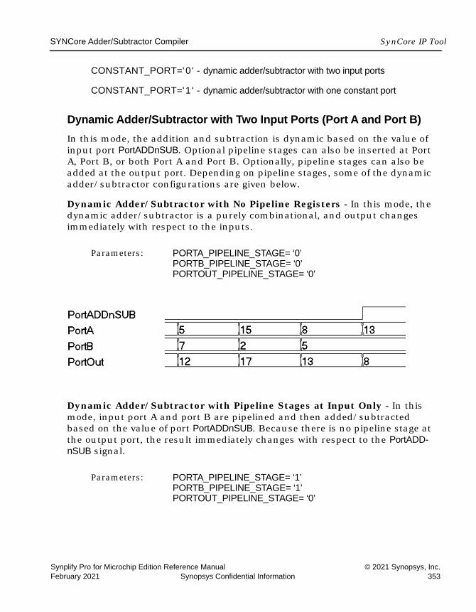
SYNCore Adder/Subtractor Compiler SynCore IP Tool
Synplify Pro for Microchip Edition Reference Manual © 2021 Synopsys, Inc.February 2021 Synopsys Confidential Information 353
CONSTANT_PORT='0 ' - dynamic adder/subtractor with two input ports
CONSTANT_PORT='1 ' - dynamic adder/subtractor with one constant port
Dynamic Adder/Subtractor with Two Input Ports (Port A and Port B)In this mode, the addition and subtraction is dynamic based on the value of input port PortADDnSUB. Optional pipeline stages can also be inserted at Port A, Port B, or both Port A and Port B. Optionally, pipeline stages can also be added at the output port. Depending on pipeline stages, some of the dynamic adder/subtractor configurations are given below.
Dynamic Adder/Subtractor with No Pipeline Registers - In this mode, the dynamic adder/subtractor is a purely combinational, and output changes immediately with respect to the inputs.
Dynamic Adder/Subtractor with Pipeline Stages at Input Only - In this mode, input port A and port B are pipelined and then added/subtracted based on the value of port PortADDnSUB. Because there is no pipeline stage at the output port, the result immediately changes with respect to the PortADD-nSUB signal.
Parameters: PORTA_PIPELINE_STAGE= ‘0’PORTB_PIPELINE_STAGE= ‘0’PORTOUT_PIPELINE_STAGE= ‘0’
Parameters: PORTA_PIPELINE_STAGE= ‘1’PORTB_PIPELINE_STAGE= ‘1’PORTOUT_PIPELINE_STAGE= ‘0’

LO
SynCore IP Tool SYNCore Adder/Subtractor Compiler
© 2021 Synopsys, Inc. Synplify Pro for Microchip Edition Reference Manual354 Synopsys Confidential Information February 2021
Dynamic Adder/Subtractor with Pipeline Stages at Input and Output - In this mode, input port A and port B are pipelined and then added/subtracted based on the value of port PortADDnSUB. Because the output port is pipelined, the result is valid only on the second rising edge of the clock.
Dynamic Adder/Subtractor with a Port ConstantIn this mode, a constant value is either added or subtracted from port A based on input port value PortADDnSUB (the constant value can be passed though the parameter CONSTANT_VALUE). Optional pipeline stages can also be inserted at port A, Optionally, pipeline stages can also be added at the output port. Depending on the pipeline stages, a number of the dynamic adder/subtractor configurations are given below (here CONSTANT_VALUE=’1’).
Parameters: PORTA_PIPELINE_STAGE= ‘1’PORTB_PIPELINE_STAGE= ‘1’PORTOUT_PIPELINE_STAGE= ‘1’
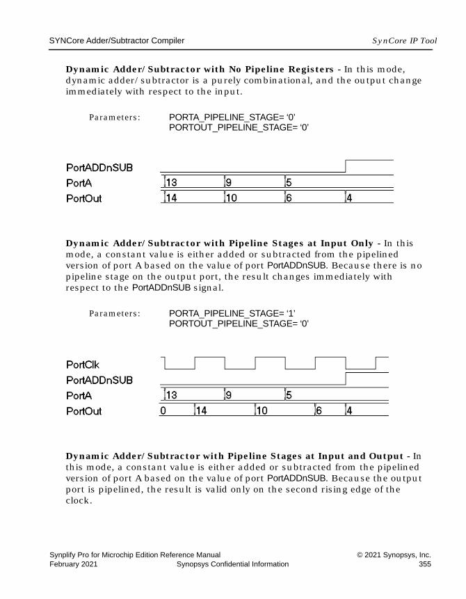
SYNCore Adder/Subtractor Compiler SynCore IP Tool
Synplify Pro for Microchip Edition Reference Manual © 2021 Synopsys, Inc.February 2021 Synopsys Confidential Information 355
Dynamic Adder/Subtractor with No Pipeline Registers - In this mode, dynamic adder/subtractor is a purely combinational, and the output change immediately with respect to the input.
Dynamic Adder/Subtractor with Pipeline Stages at Input Only - In this mode, a constant value is either added or subtracted from the pipelined version of port A based on the value of port PortADDnSUB. Because there is no pipeline stage on the output port, the result changes immediately with respect to the PortADDnSUB signal.
Dynamic Adder/Subtractor with Pipeline Stages at Input and Output - In this mode, a constant value is either added or subtracted from the pipelined version of port A based on the value of port PortADDnSUB. Because the output port is pipelined, the result is valid only on the second rising edge of the clock.
Parameters: PORTA_PIPELINE_STAGE= ‘0’PORTOUT_PIPELINE_STAGE= ‘0’
Parameters: PORTA_PIPELINE_STAGE= ‘1’PORTOUT_PIPELINE_STAGE= ‘0’

LO
SynCore IP Tool SYNCore Adder/Subtractor Compiler
© 2021 Synopsys, Inc. Synplify Pro for Microchip Edition Reference Manual356 Synopsys Confidential Information February 2021
Dynamic Adder/Subtractor with Carry InputThe following waveform shows the behavior of the dynamic adder/subtractor with a carry input (the carry input is assumed to be 0).
Dynamic Adder/Subtractor with Complete Control SignalsThe following waveform shows the complete signal set for the dynamic adder/subtractor. The enable and reset signals are always present in all of the previous cases.
Parameters: PORTA_PIPELINE_STAGE= ‘1’PORTOUT_PIPELINE_STAGE= ‘1’
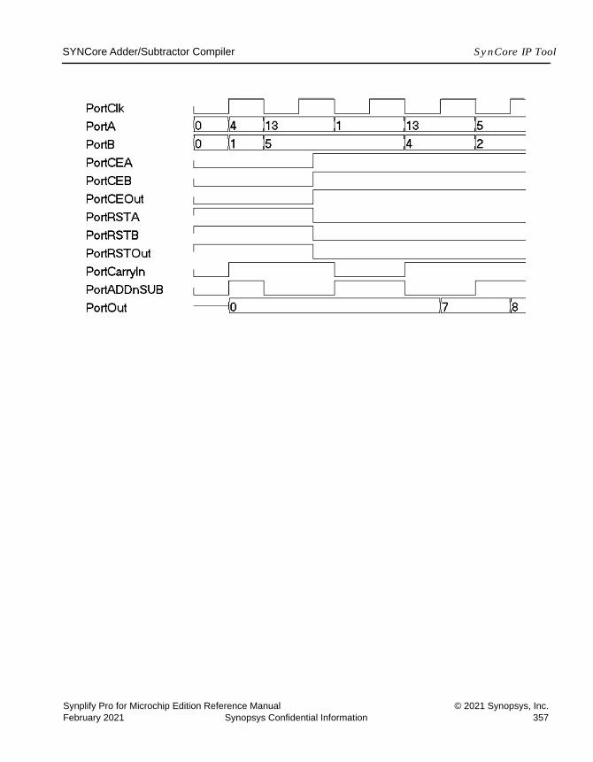
SYNCore Adder/Subtractor Compiler SynCore IP Tool
Synplify Pro for Microchip Edition Reference Manual © 2021 Synopsys, Inc.February 2021 Synopsys Confidential Information 357
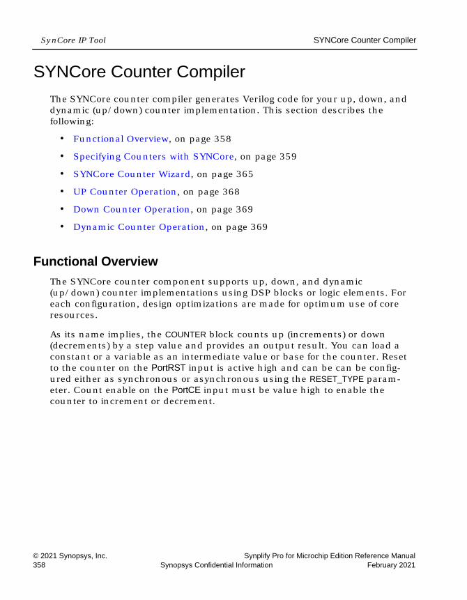
LO
SynCore IP Tool SYNCore Counter Compiler
© 2021 Synopsys, Inc. Synplify Pro for Microchip Edition Reference Manual358 Synopsys Confidential Information February 2021
SYNCore Counter Compiler The SYNCore counter compiler generates Verilog code for your up, down, and dynamic (up/down) counter implementation. This section describes the following:
• Functional Overview, on page 358
• Specifying Counters with SYNCore, on page 359
• SYNCore Counter Wizard, on page 365
• UP Counter Operation, on page 368
• Down Counter Operation, on page 369
• Dynamic Counter Operation, on page 369
Functional OverviewThe SYNCore counter component supports up, down, and dynamic (up/down) counter implementations using DSP blocks or logic elements. For each configuration, design optimizations are made for optimum use of core resources.
As its name implies, the COUNTER block counts up (increments) or down (decrements) by a step value and provides an output result. You can load a constant or a variable as an intermediate value or base for the counter. Reset to the counter on the PortRST input is active high and can be can be config-ured either as synchronous or asynchronous using the RESET_TYPE param-eter. Count enable on the PortCE input must be value high to enable the counter to increment or decrement.

SYNCore Counter Compiler SynCore IP Tool
Synplify Pro for Microchip Edition Reference Manual © 2021 Synopsys, Inc.February 2021 Synopsys Confidential Information 359
Specifying Counters with SYNCore The SYNCore IP wizard helps you generate Verilog code for your counter implementation requirements. The following procedure shows you how to generate Verilog code for a counter using the SYNCore IP wizard.
Note: The SYNCore counter model uses Verilog 2001. When adding a counter model to a Verilog-95 design, be sure to enable the Verilog 2001 check box on the Verilog tab of the Implementation Options dialog box or include a set_option -vlog_std v2001 statement in your project file to prevent a syntax error.
1. Start the wizard.
– From the FPGA synthesis tool GUI, select Run->Launch SYNCore or click the Launch SYNCore icon to start the SYNCore IP wizard.
– Ιn the window that opens, select counter_model and click Ok to open page1 of the wizard.
LO
SynCore IP Tool SYNCore Counter Compiler
© 2021 Synopsys, Inc. Synplify Pro for Microchip Edition Reference Manual360 Synopsys Confidential Information February 2021
2. Specify the parameters you need in the wizard. For details about the parameters, see Specifying Counter Parameters, on page 364. The COUNTER symbol on the left reflects any parameters you set.
3. After you have specified all the parameters you need, click the Generate button in the lower left corner.
The tool displays a confirmation message (TCL execution successful!) and writes the required files to the directory you specified on page 1 of the wizard. The HDL code is in Verilog.
SYNCore Counter Compiler SynCore IP Tool
Synplify Pro for Microchip Edition Reference Manual © 2021 Synopsys, Inc.February 2021 Synopsys Confidential Information 361
The SYNCore wizard also generates a testbench for your counter. The testbench covers a limited set of vectors. You can now close the wizard.
4. Add the counter you generated to your design.
– Edit the counter files if necessary.
– Use the Add File command to add the Verilog design file that was generated and the syncore_addnsub.v file to your project. These files are in the directory for output files that you specified on page 1 of the wizard.
– Use a text editor to open the instantiation_file.v template file. This file is located in the same output files directory. Copy the lines that define the counter and paste them into your top-level module. The following figure shows a template file (in red text) inserted into a top-level module.

LO
SynCore IP Tool SYNCore Counter Compiler
© 2021 Synopsys, Inc. Synplify Pro for Microchip Edition Reference Manual362 Synopsys Confidential Information February 2021
5. Edit the template port connections so that they agree with the port definitions in your top-level module as shown in the example below (the updated connection names are shown in red). You can also assign a unique name to each instantiation. You can also assign a unique name to each instantiation.

SYNCore Counter Compiler SynCore IP Tool
Synplify Pro for Microchip Edition Reference Manual © 2021 Synopsys, Inc.February 2021 Synopsys Confidential Information 363
module counter #(parameter COUNT_WIDTH = 5,parameter STEP = 2,parameter RESET_TYPE = 0,parameter LOAD = 2,parameter MODE = "Dynamic")
(// Output Ports
output wire [WIDTH-1:0] Count,// Input Ports
input wire Clock,input wire Reset,input wire Up_Down,input wire Load,input wire [WIDTH-1:0] LoadValue,input wire Enable);
SynCoreCounter #(.COUNT_WIDTH(COUNT_WIDTH),.STEP(STEP),.RESET_TYPE(RESET_TYPE),.LOAD(LOAD),.MODE(MODE))
SynCoreCounter_ins1 (.PortCount(Count),.PortClk(Clock),.PortRST(Reset),.PortUp_nDown(Up_Down),.PortLoad(Load),.PortLoadValue(LoadValue),.PortCE(Enable));
endmodule
Port ListThe following table lists the port assignments for all possible configurations; the third column specifies the conditions under which the port is available.

LO
SynCore IP Tool SYNCore Counter Compiler
© 2021 Synopsys, Inc. Synplify Pro for Microchip Edition Reference Manual364 Synopsys Confidential Information February 2021
Specifying Counter ParametersThe SYNCore counter can be configured for any of the following functions:
• Up Counter
• Down Counter
• Dynamic Up/Down Counter
The counter core can have a constant or variable input load or no load value. If you are creating a constant-load counter, you will need to select Enable Load and Load Constant Value on page 2 of the wizard. If you are creating a variable-load counter, you will need to select Enable Load and Use Variable Port Load on page 2. The following procedure lists the parameters you need to define when generating a counter. For descriptions of each parameter, see SYNCore Counter Wizard, on page 365.
1. Start the SYNCore counter wizard, as described in Specifying Counters with SYNCore, on page 359.
Port Name Description Required/Optional
PortCE Count Enable input pin with size one (active high)
Always present
PortClk Primary clock input Always present
PortLoad Load Enable input which loads the counter (active high).
Not present for parameter LOAD=0
PortLoadValue Load value primary input (active high)
Not present for parameter LOAD=0 and LOAD=1
PortRST Reset input which resets the counter (active high)
Always present
PortUp_nDown Primary input which determines the counter mode.0 = Up counter1 = Down counter
Present only for MODE=”Dynamic”
PortCount Counter primary output Always present

SYNCore Counter Compiler SynCore IP Tool
Synplify Pro for Microchip Edition Reference Manual © 2021 Synopsys, Inc.February 2021 Synopsys Confidential Information 365
2. Enter the following on page 1 of the wizard:
– Ιn the Component Name field, specify a name for your counter. Do not use spaces.
– In the Directory field, specify a directory where you want the output files to be written. Do not use spaces.
– Ιn the Filename field, specify a name for the Verilog file that will be generated with the counter definitions. Do not use spaces.
– Enter the width and depth of the counter in the Configure the Counter Parameters section.
– Select the appropriate configuration in the Configure the Mode of Counter section.
3. Click Next. The wizard opens page 2 where you set parameters for PortLoad and PortLoadValue.
– Select Enable Load option and the required load option in Configure Load Value section.
– Select the required reset type in the Configure Reset type section.
The COUNTER symbol dynamically updates to reflect the parameters you set.
4. Generate the counter core by clicking Generate button. All output files are written to the directory you specified on page1 of the wizard.
SYNCore Counter WizardThe following describe the parameters you can set in the ROM wizard, which opens when you select counter_model:
• SYNCore Counter Parameters Page 1, on page 366
• SYNCore Counter Parameters Page 2, on page 367
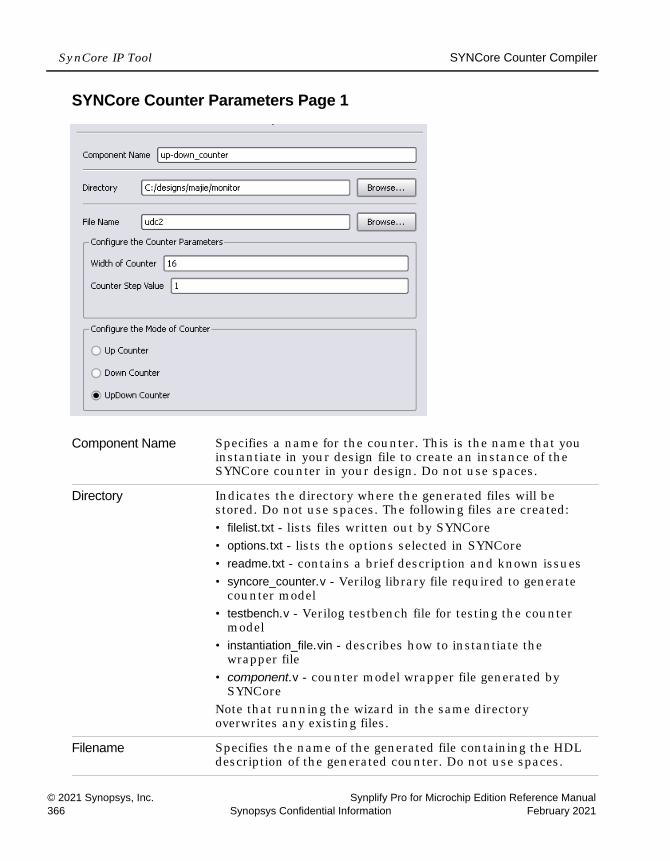
LO
SynCore IP Tool SYNCore Counter Compiler
© 2021 Synopsys, Inc. Synplify Pro for Microchip Edition Reference Manual366 Synopsys Confidential Information February 2021
SYNCore Counter Parameters Page 1
Component Name Specifies a name for the counter. This is the name that you instantiate in your design file to create an instance of the SYNCore counter in your design. Do not use spaces.
Directory Indicates the directory where the generated files will be stored. Do not use spaces. The following files are created:• filelist.txt - lists files written out by SYNCore• options.txt - lists the options selected in SYNCore• readme.txt - contains a brief description and known issues• syncore_counter.v - Verilog library file required to generate
counter model• testbench.v - Verilog testbench file for testing the counter
model• instantiation_file.vin - describes how to instantiate the
wrapper file• component.v - counter model wrapper file generated by
SYNCoreNote that running the wizard in the same directory overwrites any existing files.
Filename Specifies the name of the generated file containing the HDL description of the generated counter. Do not use spaces.

SYNCore Counter Compiler SynCore IP Tool
Synplify Pro for Microchip Edition Reference Manual © 2021 Synopsys, Inc.February 2021 Synopsys Confidential Information 367
SYNCore Counter Parameters Page 2
Width of Counter Determines the counter width (the corresponding file parameter is COUNT_WIDTH=n).
Counter Step Value Determines the counter step value (the corresponding file parameter is STEP=n).
Up Counter Specifies an up counter (the default) configuration (the corresponding file parameter is MODE=Up).
Down Counter Specifies an down counter configuration (the corresponding file parameter is MODE=Down).
UpDown Counter Specifies a dynamic up/down counter configuration (the corresponding file parameter is MODE=Dynamic).
Enable Load option Enables the load options
Load Constant Value Load the constant value specified in the Load Value for constant load option field; (the corresponding file parameter is LOAD=1).
Load Value for constant load option
The constant value to be loaded.

LO
SynCore IP Tool SYNCore Counter Compiler
© 2021 Synopsys, Inc. Synplify Pro for Microchip Edition Reference Manual368 Synopsys Confidential Information February 2021
UP Counter OperationIn this mode, the counter is incremented by the step value defined by the STEP parameter. When reset is asserted (when PostRST is active high), the counter output is reset to 0. After the assertion of PortCE, the counter starts counting upwards coincident with the rising edge of the clock. The following waveform is with a constant STEP value of 5 and no load value.
Note: Counter core can be configured to use a constant or dynamic load value in Up Counter mode (for the counter to load the Port-LoadValue, PortCE must be active). This functionality is explained in Dynamic Counter Operation, on page 369.
Use the port PortLoadValue to load Value
Loads variable value from PortLoadValue (the corresponding file parameter is LOAD=2).
Synchronous Reset Specifies a synchronous (the default) reset input (the corresponding file parameter is MODE=0).
Asynchronous Reset Specifies an asynchronous reset input (the corresponding file parameter is MODE=1).
Parameters: MODE= ‘Up’LOAD= ‘0’

SYNCore Counter Compiler SynCore IP Tool
Synplify Pro for Microchip Edition Reference Manual © 2021 Synopsys, Inc.February 2021 Synopsys Confidential Information 369
Down Counter OperationIn this mode, the counter is decremented by the step value defined by the STEP parameter. When reset is asserted (when PostRST is active high), the counter output is reset to 0. After the assertion of PortCE, the counter starts counting downwards coincident with the rising edge of the clock. The following waveform is with a constant STEP value of 5 and no load value.
Note: Counter core can be configured to use a constant or dynamic load value in Down Counter mode (for the counter to load the PortLoadValue, PortCE must be active). This functionality is explained in Dynamic Counter Operation, on page 369.
Dynamic Counter OperationIn this mode, the counter is incremented or decremented by the step value defined by the STEP parameter; the count direction (up or down) is controlled by the PortUp_nDown input (1 = up, 0 = down).
Dynamic Up/Down Counters with Constant Load Value*On de-assertion of PortRST, the counter starts counting up or down based on the PortUp_nDown input value. The following waveform is with STEP value of 5 and a LOAD_VALUE of 80. When PortLoad is asserted, the counter loads the constant load value on the next active edge of clock and resumes counting in the specified direction.
Parameters: MODE= ‘Down’LOAD= ‘0’

LO
SynCore IP Tool SYNCore Counter Compiler
© 2021 Synopsys, Inc. Synplify Pro for Microchip Edition Reference Manual370 Synopsys Confidential Information February 2021
Note: *For counter to load the PortLoadValue, PortCE must be active.
Dynamic Up/Down Counters with Dynamic Load Value*On de-assertion of PortRST, the counter starts counting up or down based on the PortUp_nDown input value. The following waveform is with STEP value of 5 and a LOAD_VALUE of 80. When PortLoad is asserted, the counter loads the constant load value on the next active edge of clock and resumes counting in the specified direction.
In this mode, the counter counts up or down based on the PortUp_nDown input value. On the assertion of PortLoad, the counter loads a new PortLoadValue and resumes up/down counting on the next active clock edge. In this example, a variable PortLoadValue of 8 is used with a counter STEP value of 5.
Parameters: MODE= ‘Dynamic’LOAD= ‘1’
Parameters: MODE= ‘Dynamic’LOAD= ‘2’
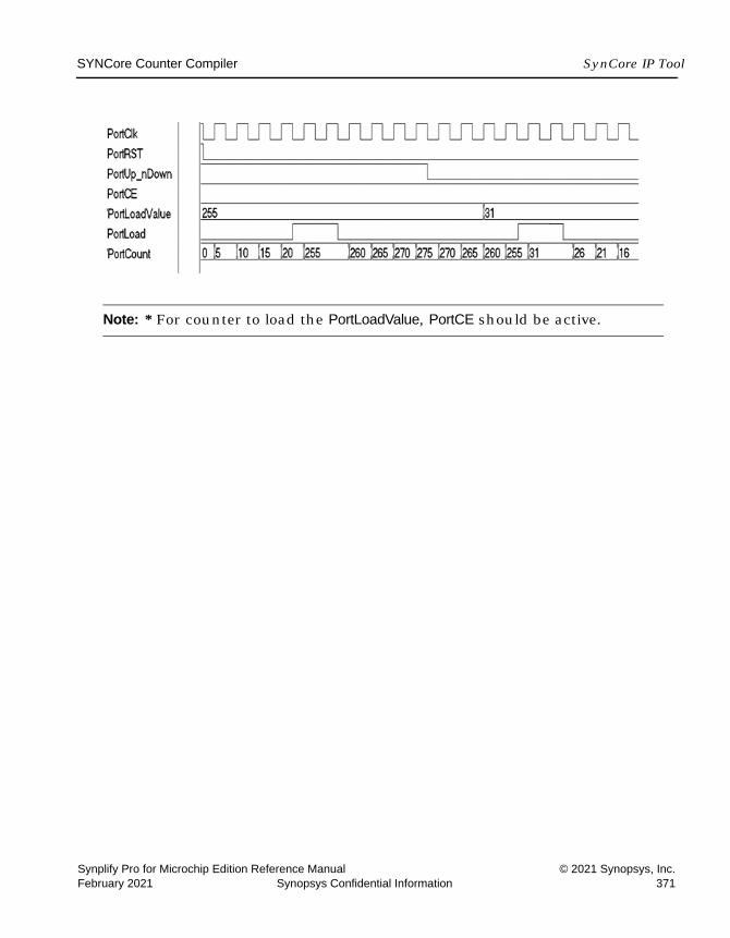
SYNCore Counter Compiler SynCore IP Tool
Synplify Pro for Microchip Edition Reference Manual © 2021 Synopsys, Inc.February 2021 Synopsys Confidential Information 371
Note: * For counter to load the PortLoadValue, PortCE should be active.

LO
SynCore IP Tool SYNCore Counter Compiler
© 2021 Synopsys, Inc. Synplify Pro for Microchip Edition Reference Manual372 Synopsys Confidential Information February 2021

Synplify Pro for Microchip Edition Reference Manual © 2021 Synopsys, Inc.February 2021 Synopsys Confidential Information 373
A P P E N D I X H
Designing with Microchip
This chapter discusses the following topics for synthesizing Microchip designs:
• Basic Support for Microchip Designs, on page 374
• Microchip Components, on page 379
• Microchip RAM Implementations, on page 388
• Microchip Constraints and Attributes, on page 408
• Microchip Device Mapping Options, on page 411
• Microchip Output Files and Forward Annotation, on page 423
• Integration with Microchip Tools and Flows, on page 427
• Microchip Attribute and Directive Summary, on page 430

LO
Designing with Microchip Basic Support for Microchip Designs
© 2021 Synopsys, Inc. Synplify Pro for Microchip Edition Reference Manual374 Synopsys Confidential Information February 2021
Basic Support for Microchip DesignsThis section describes the uses of the tool with Microchip devices. Topics include:
• Microchip Device-specific Support, on page 374
• Netlist Format, on page 374
• Microchip Features, on page 376
Microchip Device-specific SupportThe tool creates technology-specific netlists for a number of Microchip families of FPGAs. The following technologies are supported:
New devices are added on an ongoing basis. For the most current list of supported devices, check the Device panel of the Implementation Options dialog box.
Netlist FormatThe synthesis tool outputs EDIF or VM netlist files for use with the Microchip place-and-route application. These files have edn and vm extensions.
After synthesis the tool generates a constraint file as well, which is forward annotated as input into the Microchip place-and-route tool. These files have the following extensions:
FPGAs Technology Families
Mixed-Signal SmartFusion2
Low-Power • PolarFireSoC• PolarFire• IGLOO2
Rad-Tolerant RTG4
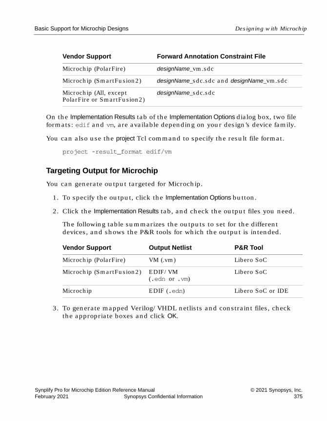
Basic Support for Microchip Designs Designing with Microchip
Synplify Pro for Microchip Edition Reference Manual © 2021 Synopsys, Inc.February 2021 Synopsys Confidential Information 375
On the Implementation Results tab of the Implementation Options dialog box, two file formats: edif and vm, are available depending on your design’s device family.
You can also use the project Tcl command to specify the result file format.
project -result_format edif/vm
Targeting Output for MicrochipYou can generate output targeted for Microchip.
1. To specify the output, click the Implementation Options button.
2. Click the Implementation Results tab, and check the output files you need.
The following table summarizes the outputs to set for the different devices, and shows the P&R tools for which the output is intended.
3. To generate mapped Verilog/VHDL netlists and constraint files, check the appropriate boxes and click OK.
Vendor Support Forward Annotation Constraint File
Microchip (PolarFire) designName_vm.sdc
Microchip (SmartFusion2) designName_sdc.sdc and designName_vm.sdc
Microchip (All, except PolarFire or SmartFusion2)
designName_sdc.sdc
Vendor Support Output Netlist P&R Tool
Microchip (PolarFire) VM (.vm) Libero SoC
Microchip (SmartFusion2) EDIF/VM(.edn or .vm)
Libero SoC
Microchip EDIF (.edn) Libero SoC or IDE

LO
Designing with Microchip Basic Support for Microchip Designs
© 2021 Synopsys, Inc. Synplify Pro for Microchip Edition Reference Manual376 Synopsys Confidential Information February 2021
Customizing Netlist FormatsThe following table lists some attributes for customizing your Microchip output netlists:
Microchip Forward AnnotationThe synthesis tool generates Microchip-compliant constraint files from selected constraints that are forward annotated (read in and then used) by the Microchip Libero SoC or Libero IDE place-and-route software. The Microchip constraint file uses the _vm.sdc or _sdc.sdc extension. This constraint file must be imported into the Microchip flow.
By default, Microchip constraint files are generated from the synthesis tool constraints. You can then forward annotate these files to the place-and-route tool. To disable this feature, deselect the Write Vendor Constraint File box (on the Implementation Results tab of the Implementation Options dialog box).
Microchip FeaturesThe synthesis tool contains the following Microchip-specific features:
• Direct mapping to Microchip c-modules and s-modules
• Timing-driven mapping, replication, and buffering
• Inference of counters, adders, and subtractors; module generation
• Automatic use of clock buffers for clocks and reset signals
• Automatic I/O insertion. See I/O Insertion, on page 412 for more information.
• CDC Reporting. See CDC Reporting below.
For ... Use ...
Netlist formatting syn_netlist_hierarchy define_global_attribute syn_netlist_hierarchy {0}
Bus specification syn_noarrayports define_global_attribute syn_noarrayports {1}

Basic Support for Microchip Designs Designing with Microchip
Synplify Pro for Microchip Edition Reference Manual © 2021 Synopsys, Inc.February 2021 Synopsys Confidential Information 377
CDC ReportingPolarFire, RTG4, SmartFusion2, IGLOO2
Reporting of Clock Domain Crossing (CDC) paths is supported. The synthesis tool identifies different types of synchronizer circuits in the design and reports these in a log report.
The following synchronizers are supported:
• n-FF synchronizer (control synchronizer)
• Mux synchronizer (data synchronizer)
The CDC report is generated in a {}_cdc.csv file.
The tool also detects and preserves Driver FF and CDC synchronizer FFs when the following attributes are set on the FFs:
syn_preserve = 1, syn_replicate = 0, syn_allow_retiming = 0
Project options
set_option -report_preserve_cdc {1/0} enables or disables CDC reporting. The option is ON, by default. The GUI option for enabling or disabling CDC reports is Report CDC paths in the High Reliability Panel.
set_option -min_cdc_sync_flops {2} controls the minimum number of synchronizer flops to be detected and reported. By default, the option is 2. Setting the value lesser than 2 generates a warning. If the number of synchronizer flops are lesser than the minimum value set in this option, then those paths are tagged as Unsafe CDC paths.
Synplify Pro adds the synchronizer attribute in the vm netlist on the FFs, as given:
(* cdc_synchronizer = 1 *)The cdc_synchronizer property is not forward annotated in case the CDC is unsafe.
unsafe_cdc_netlist_property enables forward annotation of the cdc_synchronizer property even if the path is unsafe. To enable the option, set the value to 1 as given below. By default, the value is set to 0.
set_option -unsafe_cdc_netlist_property 1

LO
Designing with Microchip Basic Support for Microchip Designs
© 2021 Synopsys, Inc. Synplify Pro for Microchip Edition Reference Manual378 Synopsys Confidential Information February 2021
Unsafe Path Reporting
The following describe different scenarios in which a CDC path may be reported as unsafe:
• No synchronizer circuit detected
– When control signals (reset, enable, set) on the first and the second sync registers do not match.
– Combinational logic is present between the first and the second flop synchronizers.
– Diversion between the first and the second flop synchronizers which means fanout is greater than 1.
– Only 1 flop in the synchronizer circuit.
• Number of register levels in the synchronizer logic is lesser than the \"min_cdc_sync_flops\" threshold. For example, if min_cdc_sync_flops is set to 3 and levels of the synchronizer flop is 2.
• Combinatorial logic detected at clock domain crossing
Combinatorial logic is present between the source register (start instance) and the destination register (end instance) at the crossover.
• Divergence detected in the crossover path
Source register (start instance) has fanout greater than 1 at the cross-over.
• Enable signal for synchronizer registers does not have a safe crossing
Enable of data synchronizer doesn’t have a safe synchronizer circuit.
• Sources from different domains in fanin
The destination is driven by multiple registers from different clock domains and they are asynchronous to the destination register clock domain.
• Synchronizer registers have synchronous reset or set as control signal
The synchronizer registers have a synchronous set or reset even if shared by all. This is tagged as unsafe since the reset logic can move to the data path instead of connecting to the reset port of the register, leading to metastability.
Microchip Components Designing with Microchip
Synplify Pro for Microchip Edition Reference Manual © 2021 Synopsys, Inc.February 2021 Synopsys Confidential Information 379
Microchip ComponentsThese topics describe how the synthesis tool handles various Microchip components, and show you how to work with or manipulate them during synthesis to get the results you need:
• Macros and Black Boxes in Microchip Designs, on page 379
• DSP Block Inference, on page 381
• Control Signals Extraction for Registers (SLE), on page 386
• Wide MUX Inference, on page 387
Macros and Black Boxes in Microchip DesignsYou can instantiate Smartgen1 macros or other Microchip macros like gates, counters, flip-flops, or I/Os by using the supplied Microchip macro libraries to pre-define the Microchip macro black boxes. For certain technologies, the following macros are also supported:
• MACC and RAM Timing Models
• SmartFusion2 MACC Block
• SIMBUF Macro
For general information on instantiating black boxes, see Instantiating Black Boxes in VHDL, on page 403, and Instantiating Black Boxes in Verilog, on page 122. For specific procedures about instantiating macros and black boxes and using Microchip black boxes, see the following sections in the User Guide:
• Defining Black Boxes for Synthesis, on page 382
• Using Predefined Microchip Black Boxes, on page 428
• Using Smartgen Macros, on page 429
1. Smartgen macros now replace the ACTgen macros. ACTgen macros were availablein the previous Designer 6.x place-and-route tool.
LO
Designing with Microchip Microchip Components
© 2021 Synopsys, Inc. Synplify Pro for Microchip Edition Reference Manual380 Synopsys Confidential Information February 2021
MACC and RAM Timing Models
MACC and RAM timing models are supported for PolarFire, RTG4, SmartFu-sion2, and IGLOO2 devices. Timing analysis considers the timing arcs for RAM and MACC.
SmartFusion2 MACC BlockSmartFusion2 devices support bit-signed 18x18 multiply-accumulate blocks. This architecture provides dedicated components called SmartFusion2 MACC blocks, for which DSP-related operations can be performed like multiplication followed by addition, multiplication followed by subtraction, and multiplica-tion with accumulate. For more information, see DSP Block Inference, on page 381.
SIMBUF MacroThe synthesis software supports instantiation of the SIMBUF macro. The SIMBUF macro provides the flexibility to probe signals without using physical locations, as possible from the Identify tool. The Resource Summary will report the number of SIMBUF instantiations in the IO Tile section of the log file.

Microchip Components Designing with Microchip
Synplify Pro for Microchip Edition Reference Manual © 2021 Synopsys, Inc.February 2021 Synopsys Confidential Information 381
DSP Block InferenceThis feature allows the synthesis tool to infer DSP or MATH18x18 blocks for SmartFusion2 devices and MACC_PA block for PolarFire devices. The following structures are supported for SmartFusion2 devices:
• DOTP Support
The MACC block is configured in DOTP mode when two independent signed 9-bit x 9-bit multipliers are followed by addition. The sum of the dual independent 9x9 multiplier (DOTP) result is stored in the upper 35 bits of the 44-bit output. In DOTP mode, the MACC block implements the following equation:
P = D + (CARRYIN + C) + 512 * ((AL * BH)+ (AH * BL)), when SUB = 0
P = D + (CARRYIN + C) - 512 * ((AL * BH) + (AH * BL)), when SUB = 1
Below is an example RTL which infers MACC block in DOTP mode after synthesis:
module dotp_add_unsign_syn (ina, inb, inc, ind, ine, dout);parameter widtha = 6;parameter widthb = 7;parameter widthc = 7;parameter widthd = 8;parameter widthe = 30;parameter width_out = 44;
input [widtha-1:0] ina;input [widthb-1:0] inb;input [widthc-1:0] inc;input [widthd-1:0] ind;input [widthe-1:0] ine;output reg [width_out-1:0] dout;always @(ina or inb or inc or ind or ine)
begindout <= (ina * inb) + (inc * ind) + ine;
end endmoduleThe MACC block does not support DOTP mode if the
– Width of the multiplier inputs is greater than 9-bits when signed.
– Width of the multiplier inputs is greater than 8-bits when unsigned.
– Width of the non-multiplier inputs is greater than 36-bits.

LO
Designing with Microchip Microchip Components
© 2021 Synopsys, Inc. Synplify Pro for Microchip Edition Reference Manual382 Synopsys Confidential Information February 2021
• Multipliers
• Mult-adds — Multiplier followed by an Adder
• Mult-subs — Multiplier followed by a Subtractor
• Wide multiplier inference
A multiplier is treated as wide, if any of its inputs is larger than 18 bits signed or 17 bits unsigned. The multiplier can be configured with only one input that is wide, or else both inputs are wide. Depending on the number of wide inputs for signed or unsigned multipliers, the synthesis software uses the cascade feature to determine how many math blocks to use and the number of Shift functions it needs.
• MATH block inferencing across hierarchy
This enhancement to MATH block inferencing allows packing input registers, output registers, and any adders or subtractors into different hierarchies. This helps to improve QoR by packing logic more efficiently into MATH blocks.
By default, the synthesis software maps the multiplier to DSP blocks if all inputs to the multiplier are more than 2-bits wide; otherwise, the multiplier is mapped to logic. You can override this default behavior using the syn_multstyle attribute. See syn_multstyle, on page 129 for details.
The following conditions also apply:
• Signed and unsigned multiplier inferencing is supported.
• Registers at inputs and outputs of multiplier/multiplier-adder/multi-plier-subtractor are packed into DSP blocks.
• Synthesis software fractures multipliers larger than 18X18 (signed) and 17X17 (unsigned) into smaller multipliers and packs them into DSP blocks.
• When multadd/multsub are fractured, the final adder/subtractor are packed into logic.
The following structures are supported for PolarFire devices:
• Add-mult — Adder followed by a Multiplier
• Multipliers
• Mult-adds — Multiplier followed by an Adder
Microchip Components Designing with Microchip
Synplify Pro for Microchip Edition Reference Manual © 2021 Synopsys, Inc.February 2021 Synopsys Confidential Information 383
• Mult-subs — Multiplier followed by a Subtractor
• Mult-acc — Multiplier followed by an Accumulator
• Wide multiplier inference
• MATH block inferencing across hierarchy
• DOTP Support
• Coefficient ROM
This section also includes the following topics:
• Packing Coefficient ROM in the DSP, on page 383
• DSP Cascade Chain Inference, on page 384
• Symmetric FIR Filter Packing in MACC_PA_BC_ROM, on page 384
• Multiplier-Accumulators (MACC) Inference, on page 385
Packing Coefficient ROM in the DSPPacking the coefficient ROM in the DSP implements the coefficient ROM data as one input to mult-add/add/sub, when inferring the MACC_PA_BC_ROM macro. The MACC_PA_BC_ROM macro extends the functionality of the MACC_PA macro to provide a 16x18 ROM at the A input. The USE_ROM pin is available for the primitive to select the input data A or the ROM data at ROM_ADDR.
Select operand A as follows:
• When USE_ROM = 0, select input data A.
• When USE_ROM = 1, select the ROM data at ROM_ADDR.
The RTL example below infers the MACC_PA_BC_ROM macro after synthesis:
module test(in1, rom_addr, out);parameter data_width = 17;parameter rom_width = 17;parameter rom_depth = 4;input [data_width-1:0] in1;input [rom_depth-1:0] rom_addr;output [47:0] out;

LO
Designing with Microchip Microchip Components
© 2021 Synopsys, Inc. Synplify Pro for Microchip Edition Reference Manual384 Synopsys Confidential Information February 2021
reg [rom_width-1:0] mem [0:2**rom_depth -1];wire [rom_width-1:0] rom_data;initialbegin
$readmemb("mem.dat", mem);endassign rom_data = mem [rom_addr];assign out = rom_data * in1;endmodule
DSP Cascade Chain Inference The MATH18x18 block cascade feature supports the implementation of multi-input Mult-Add/Sub for devices with MATH blocks. The software packs logic into MATH blocks efficiently using hard-wired cascade paths, which improves the QoR for the design.
Prerequisites include the following requirements:
• The input size for multipliers is not greater than 18x18 bits (signed) and 17x17 bits (unsigned).
• Signed multipliers have the proper sign-extension.
• All multiplier output bits feed the adder.
• Multiplier inputs and outputs can be registered or not.
Symmetric FIR Filter Packing in MACC_PA_BC_ROMPolarFire
The tool supports the packing of symmetric FIR filters though the inference of MACC_PA_BC_ROM blocks with shift chain.
Microchip Components Designing with Microchip
Synplify Pro for Microchip Edition Reference Manual © 2021 Synopsys, Inc.February 2021 Synopsys Confidential Information 385
Multiplier-Accumulators (MACC) Inference The Multiplier-Accumulator structures use internal paths for adder feedback loops inside the MATH18x18 block instead of connecting it externally.
Prerequisites include the following requirements:
• The input size for multipliers is not greater than 18x18 bits (signed) and 17x17 bits (unsigned).
• Signed multipliers have the proper sign-extension.
• All multiplier output bits feed the adder.
• The output of the adder must be registered.
• The registered output of the adder feeds back to the adder for accumula-tion.
• Since the Microchip MATH block contains one multiplier, only Multi-plier-Accumulator structures with one multiplier can be packed inside the MATH block.
The other Multiplier-Accumulator structure supported is with Synchronous Loadable Register.
Prerequisites include the following requirements:
• All the requirements mentioned above apply for this structure as well.
• For the Loading Multiplier-Accumulator structure, new Load data should be passed to input C.
• The LoadEn signal should be registered.
DSP Limitations
Currently, DSP inferencing does not support the following functions:
• Overflow extraction
• Arithmetic right shift for operand C
LO
Designing with Microchip Microchip Components
© 2021 Synopsys, Inc. Synplify Pro for Microchip Edition Reference Manual386 Synopsys Confidential Information February 2021
Note: For more information about Microchip DSP math blocks along with a comprehensive set of examples, see the Inferring Microchip RTAX-DSP MATH Blocks application note on the Synopsys website.
Control Signals Extraction for Registers (SLE)The synthesis software supports extraction of control signals, the enable, synchronous set or reset, and asynchronous reset on the registers. The tool packs the enable with the EN pin, synchronous set or reset using SLn pin and asynchronous reset using ALn pin of the SLE.
When the fanout limit is 12, synchronous set or reset is packed using the SLn pin. If the fanout limit is less than 12, the tool inserts extra logic for the synchronous set or reset.
The tool supports packing of the enable signal, which has higher priority than the reset signal (synchronous) of the SLE.
Initial Values for Registers (SLE)Initial values are not supported on registers (SLE). If the initial value is specified for a register in the RTL code, the tool ignores the value and issues a warning. For the following Verilog code:
module testinput clk,input [7:0] a,output [7:0] z);reg [7:0] z_reg = 8'hf0;reg one = 1'd1;always@(posedge clk)z_reg <= a + one;assign z = z_reg;endmodule
The initial value for register z_reg is specified, so the tool issues a warning message in the synthesis log report:
@W: FX1039|User-specified initial value defined for instance z_reg[7:0] is being ignored.
Microchip Components Designing with Microchip
Synplify Pro for Microchip Edition Reference Manual © 2021 Synopsys, Inc.February 2021 Synopsys Confidential Information 387
Wide MUX InferenceWide MUXs are implemented using ARI1 primitives and is supported for PolarFire, RTG4, and SmartFusion2 technologies.

LO
Designing with Microchip Microchip RAM Implementations
© 2021 Synopsys, Inc. Synplify Pro for Microchip Edition Reference Manual388 Synopsys Confidential Information February 2021
Microchip RAM ImplementationsRefer to the following topics for Microchip RAM implementations:
• RAM for PolarFire
• RAM for RTG4
• RAM for SmartFusion2/IGLOO2
• PolarFire Asymmetric RAM support
• RAM Reporting
• Low Power RAM Inference
• URAM Inference for Sequential Shift Registers
• Async Reset and Dynamic Offset in Seqshifts
• Packing of Enable Signal on the Read Address Register
• Packing of INIT Value on LSRAM and URAM Blocks in PolarFire
• PolarFire RAM Inference for ROM Support
• Write Byte-Enable Support for RAM
• RAMINDEX Support
RAM for PolarFireThe tool supports the following RAM primitives for the PolarFire device:
• RAM1K20 (LSRAM) is supported for both inference and instantiation.
The following configurations are supported for inference:
– True dual-port configuration
– Dual-port ROM
– Two independent data ports
– Non-ECC—1Kx20, 2Kx10, 4Kx5, 8Kx2 or 16Kx1 on each port
– Two-port configuration
– Read from port A and write to port B
Microchip RAM Implementations Designing with Microchip
Synplify Pro for Microchip Edition Reference Manual © 2021 Synopsys, Inc.February 2021 Synopsys Confidential Information 389
– Non-ECC—512x40, 1Kx20, 2Kx10, 4Kx5, 8Kx2 or 16Kx1 on each port
– ECC—512x33 on both ports
Generates SB_CORRECT and DB_DETECT flags
– Write operations
Three modes—simple write, write feed-through, read before write
– Asymmetric RAM is supported. See PolarFire Asymmetric RAM support, on page 394.
• RAM64x12 (USRAM) is supported for both inference and instantiation.
The following configurations are supported for inference:
– The RAM64x12 block contains 768 memory bits and is a two-port memory, providing one write port and one read port. Write operations for the RAM64x12 memory are synchronous. Read operations can be asynchronous or synchronous to set up the address and read out the data.
– Consists of one read-data port and one write-data port.
– Both read-data and write-data ports are configured to 64x12.
RAM for RTG4The software supports the following RAM primitives for the RTG4 device:
RAM1K18_RT Maps to RAM1K18_RT for:• Single-port, two-port, and dual-port synchronous read/write
memory.• Read-before-write in dual-port mode for single-port and dual-
port synchronous memory.• Read-enable extraction1.
1. Currently, read-enable extraction for wide RAM is not supported.
RAM64X18_RT Maps to RAM64X18_RT for single-port, two-port, and three-port synchronous/asynchronous read and synchronous write memory.
LO
Designing with Microchip Microchip RAM Implementations
© 2021 Synopsys, Inc. Synplify Pro for Microchip Edition Reference Manual390 Synopsys Confidential Information February 2021
Read-before-write mode not supported for RAM1K18_RT primitive of RTG4Read-before-write mode is not supported for the RTG4 RAM1K18_RT RAM primitive. By default, when Read/Write Check insertion is OFF, RAM1K18_RT is inferred in the mode in which Read-data port holds the previous value, with A_WMODE/B_WMODE set to 00.
When Read/Write Check insertion is ON, true dual-port RAM in Read-before-write mode errors out due to multiple write clocks or is implemented as registers if a single clock is present. Single-port RAM in Read-before-write mode is inferred as RAM64x18_RT and logic.
RAM for SmartFusion2/IGLOO2 Two types of RAM macros are supported: RAM1K18 and RAM64X18. The synthesis software extracts the RAM structure from the RTL and infers RAM1K18 or RAM64X18 based on the size of the RAM.
The default criteria for specifying the macro is described in the table below for the following RAM types.
True Dual-Port Synchronous Read Memory
The synthesis tool maps to RAM1K18, regardless of its memory size.
Microchip RAM Implementations Designing with Microchip
Synplify Pro for Microchip Edition Reference Manual © 2021 Synopsys, Inc.February 2021 Synopsys Confidential Information 391
You can override the default behavior by applying the syn_ramstyle attribute to control how the memory gets mapped. To map to
• RAM1K18 set syn_ramstyle = "lsram"• RAM64X18 set syn_ramstyle = "uram"
• Registers set syn_ramstyle = "registers"
The value you set for this attribute always overrides the default behavior.
Three-Port RAM Inference Support
Verilog Example 1: Three-Port RAM—Synchronous Read module ram_infer15_rtl
(clk,dinc,douta,doutb,wrc,rda,rdb,addra,addrb,addrc);input clk;input [17:0] dinc;input wrc,rda,rdb;input [5:0] addra,addrb,addrc;output [17:0] douta,doutb;reg [17:0] douta,doutb;reg [17:0] mem [0:63];
Simple Dual-Port or Single-Port Synchronous Memory
If the size of the memory is:• 4608 bits or greater, the synthesis tool maps to
RAM1K18.• Greater than 12 bits and less than 4608 bits, the
synthesis tool maps to RAM64X18.• Less than or equal to 12 bits, the synthesis tool
maps to registers.
Simple Dual-Port or Single-Port Asynchronous Memory
When the size of the memory is 12 bits or greater, the synthesis tool maps to RAM64x18. Otherwise, it maps to registers.
Three-Port RAM Inference Support
This feature supports SmartFusion2 and IGLOO2 devices only.• RAM64x18 is a 3-port memory that provides one
Write port and two Read ports.• Write operation is synchronous, while read
operations can be asynchronous or synchronous.The tool infers RAM64X18 for these structures.
LO
Designing with Microchip Microchip RAM Implementations
© 2021 Synopsys, Inc. Synplify Pro for Microchip Edition Reference Manual392 Synopsys Confidential Information February 2021
always@(posedge clk)beginif(wrc)mem[addrc] <= dinc;endalways@(posedge clk)begindouta <= mem[addra];endalways@(posedge clk)begindoutb <= mem[addrb] ;endendmodule

Microchip RAM Implementations Designing with Microchip
Synplify Pro for Microchip Edition Reference Manual © 2021 Synopsys, Inc.February 2021 Synopsys Confidential Information 393
RTL View:
The tool infers one RAM64X18.
VHDL Example 2: Three-Port RAM—Asynchronous Readlibrary ieee; use ieee.std_logic_1164.all; use ieee.std_logic_unsigned.all; entity ram_singleport_noreg is port (d : in std_logic_vector(7 downto 0); addw : in std_logic_vector(6 downto 0); addr1 : in std_logic_vector(6 downto 0); addr2 : in std_logic_vector(6 downto 0); we : in std_logic; clk : in std_logic; q1 : out std_logic_vector(7 downto 0); q2 : out std_logic_vector(7 downto 0)); end ram_singleport_noreg; architecture rtl of ram_singleport_noreg is type mem_type is array (127 downto 0) of std_logic_vector (7 downto 0); signal mem: mem_type; begin process (clk) begin if rising_edge(clk) then if (we = '1') then mem(conv_integer (addw)) <= d; end if;
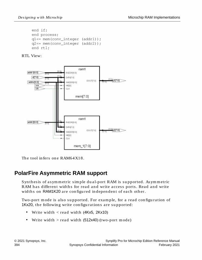
LO
Designing with Microchip Microchip RAM Implementations
© 2021 Synopsys, Inc. Synplify Pro for Microchip Edition Reference Manual394 Synopsys Confidential Information February 2021
end if; end process; q1<= mem(conv_integer (addr1)); q2<= mem(conv_integer (addr2)); end rtl;
RTL View:
The tool infers one RAM64X18.
PolarFire Asymmetric RAM supportSynthesis of asymmetric simple dual-port RAM is supported. Asymmetric RAM has different widths for read and write access ports. Read and write widths on RAM1K20 are configured independent of each other.
Two-port mode is also supported. For example, for a read configuration of 1Kx20, the following write configurations are supported:
• Write width < read width (4Kx5, 2Kx10)
• Write width > read width (512x40) (two-port mode)

Microchip RAM Implementations Designing with Microchip
Synplify Pro for Microchip Edition Reference Manual © 2021 Synopsys, Inc.February 2021 Synopsys Confidential Information 395
Example 1—When Write Width < Read WidthIn the RTL below, write access configuration is 2Kx8 and read access configuration is 1Kx16.
module asym_ram (din ,dout, addra, addrb, clk, wen); input [7:0] din; input wen;input [10:0] addra; output reg [15:0] dout; input [9:0] addrb; input clk; localparam ratio= 2; localparam max_depth=2048; localparam min_width=8; reg [10:0] taddra;reg [min_width-1:0] mem_ram[max_depth-1:0]; always @(posedge clk) begin
if(wen) mem_ram[taddra]<=din; taddra<=addra;
end always @(posedge clk) begin // manual concatenation
dout[min_width*0+:min_width]<=mem_ram[{0,addrb}]; // it can be written inside generate-loop
dout[min_width*1+:min_width]<=mem_ram[{1,addrb}]; end endmodule

LO
Designing with Microchip Microchip RAM Implementations
© 2021 Synopsys, Inc. Synplify Pro for Microchip Edition Reference Manual396 Synopsys Confidential Information February 2021
RTL View
Technology View

Microchip RAM Implementations Designing with Microchip
Synplify Pro for Microchip Edition Reference Manual © 2021 Synopsys, Inc.February 2021 Synopsys Confidential Information 397
Example 2—When Write Width > Read WidthThe code below implements asymmetric RAM with 1Kx16 write access and 2Kx8 read access configurations.
module asym_ram(din, dout, addra, addrb, clk, we); input [15:0] din; input [9:0] addra; output reg [7:0] dout; input [10:0] addrb; input clk; input we; localparam max_depth=2048; localparam min_width=8; reg [min_width-1:0] mem_ram[max_depth-1:0]; reg [9:0] taddra; reg [10:0] taddrb; always @(posedge clk) begin dout<=mem_ram[taddrb]; taddrb<=addrb; end always @(posedge clk) if (we) begin mem_ram[{0,addra}]<=din[min_width*0+:min_width]; mem_ram[{1,addra}]<=din[min_width*1+:min_width]; end endmodule

LO
Designing with Microchip Microchip RAM Implementations
© 2021 Synopsys, Inc. Synplify Pro for Microchip Edition Reference Manual398 Synopsys Confidential Information February 2021
RTL View
Technology View
Microchip RAM Implementations Designing with Microchip
Synplify Pro for Microchip Edition Reference Manual © 2021 Synopsys, Inc.February 2021 Synopsys Confidential Information 399
AttributesRAM attributes, like syn_ramstyle, are applied to control the inference.
Read Write Control SignalsControl signals are the same as that of symmetric RAM implementation:
• Enable read and write
• Synchronous and asynchronous reset on RAM registers
• RAM read-write mode (no change, write-first, read-first)
• Packing of RAM registers or pipelines
Limitations• Initial value is not supported.
• Asymmetric true dual-port RAM is not supported.
• Read/write logic check creation is not supported. If the read/write check option is enabled, then the RAM is implemented in symmetric mode.
RAM ReportingA detailed report is generated in the {implname}_ram_rpt.txt file with details of the LSRAM and URAMs inferred for a design.
LO
Designing with Microchip Microchip RAM Implementations
© 2021 Synopsys, Inc. Synplify Pro for Microchip Edition Reference Manual400 Synopsys Confidential Information February 2021
Low Power RAM Inference PolarFire, RTG4, SmartFusion2, and IGLOO2 Technologies
Enhanced RAM inference uses the BLK pin of the RAM for reducing power consumption. By setting the global option low_power_ram_decomp 1 in the project file, the tool fractures the wide RAMs on the address width, using the BLK pin of the RAM to reduce power consumption. By default, the tool fractures wide RAMs by splitting the data width to improve timing.
This feature is supported for single-port, simple-dual port, and true-dual port RAM modes.
URAM Inference for Sequential Shift RegistersPolarFire Technologies
URAM inference is supported for sequential shift registers.
By default, seqshift is implemented using registers. The syn_srlstyle attribute is used to override the default behavior of seqshift implementation using URAM. This attribute can be applied on the top-level module or on a seqshift instance in the RTL view, by dragging and dropping the instance to the SCOPE editor.
If the attribute is applied on the top-level module, the tool infers URAM for all the seqshifts in the design using the following threshold values:
Depth >= 4 and Depth*Width > 36
If the attribute is applied on the seqshift instance, the tool infers URAM irrespective of the threshold values.
syn_srlstyle Values
Value Description
Registers seqshifts are inferred as registers.
URAM seqshift is inferred as RAM64X12.
Microchip RAM Implementations Designing with Microchip
Synplify Pro for Microchip Edition Reference Manual © 2021 Synopsys, Inc.February 2021 Synopsys Confidential Information 401
syn_srlstyle Syntax
ExampleThe tool infers a seqshift primitive for the following HDL:
module p_seqshift(clk, we, din, dout); parameter SRL_WIDTH = 7; parameter SRL_DEPTH = 37; input clk, we; input [SRL_WIDTH-1:0] din; output [SRL_WIDTH-1:0] dout; reg [SRL_WIDTH-1:0] regBank[SRL_DEPTH-1:0]
/*synthesis syn_srlstyle = "uram"*/; integer i; always @(posedge clk) begin
if (we) beginfor (i=SRL_DEPTH-1; i>0; i=i-1) begin
regBank[i] <= regBank[i-1]; end regBank[0] <= din;
endend assign dout = regBank[SRL_DEPTH-1]; endmodule
The seqshift generated for the HDL above is shown in technology view.
FDC define_attribute {object} syn_srlstyle {registers|uram }define_global_attribute syn_srlstyle {registers|uram }
Verilog object /* synthesis syn_srlstyle = "registers | uram " */;
VHDL attribute syn_srlstyle : string;attribute syn_srlstyle of object : signal is "registers | uram ";

LO
Designing with Microchip Microchip RAM Implementations
© 2021 Synopsys, Inc. Synplify Pro for Microchip Edition Reference Manual402 Synopsys Confidential Information February 2021
LimitationsLimitations include the following:
• Seqshifts with both reset and set are inferred as registers.
• Seqshifts with enable signal having higher priority than synchronous set or synchronous reset are inferred as registers.
Async Reset and Dynamic Offset in SeqshiftsThe tool supports the packing of async reset and dynamic offset logic in seqshifts through the inference of RAM blocks in PolarFire devices.
Packing of Enable Signal on the Read Address RegisterPolarFire and RTG4 Technologies
The tool packs the enable signal on the read address register for the following:
• PolarFire RAM1K20 and RAM64x12 Enhancements
• RTG4 RAM64x18, RAM64x18_RT, RAM1K18_RT Enhancements
Microchip RAM Implementations Designing with Microchip
Synplify Pro for Microchip Edition Reference Manual © 2021 Synopsys, Inc.February 2021 Synopsys Confidential Information 403
PolarFire RAM1K20 and RAM64x12 EnhancementsThe tool supports the packing of enable signal on the read address register into RAM1K20 (A_REN) and RAM64x12 (R_ADDR_EN).
RTG4 RAM64x18, RAM64x18_RT, RAM1K18_RT EnhancementsPacking of enable signal on the read address register into RAM1K18_RT (A_REN), RAM64x18 (A_ADDR_EN & B_ADDR_EN), and RAM64x18_RT (A_ADDR_EN & B_ADDR_EN) is supported.
Packing of INIT Value on LSRAM and URAM Blocks in PolarFireINIT value packing is supported for RAM1K20 and RAM64x12 RAM blocks in the PolarFire device. Here is some sample code:
module test (clk,we,waddr,raddr,din,q);input clk,we;input [addr_width - 1 : 0] waddr,raddr;input [data_width - 1 : 0] din;output [data_width - 1 : 0] q;reg [data_width - 1 : 0] q;reg [data_width - 1 : 0] mem [(2**addr_width) - 1 : 0];initial $readmemb("mem1.dat", mem);always @ (posedge clk) if(we) mem[waddr] <= din;always @ (posedge clk ) if(we) q <= din; else q <= mem[raddr]; endmodule
PolarFire RAM Inference for ROM SupportBy default, ROM is implemented using RAM1K20 and RAM64x12 depending on the RAM threshold values. The RAM is inferred in non-low (speed) mode. Asynchronous ROM is always mapped to RAM64x12.
Use the syn_romstyle attribute to override the default behavior of the ROM implementation with RAM or logic.
LO
Designing with Microchip Microchip RAM Implementations
© 2021 Synopsys, Inc. Synplify Pro for Microchip Edition Reference Manual404 Synopsys Confidential Information February 2021
The syn_romstyle attribute can be used to determine the implementation of the ROM components as follows:
The syn_romstyle values are:
Example 1module test(clk,addr,dataout);input clk;parameter addr_width = 10;parameter data_width = 20;input [addr_width-1:0] addr;output [data_width-1:0] dataout;reg [data_width-1:0] dataout;always @ (posedge clk )case (addr)10'd0 : dataout <= 20'b01000110000010001100;10'd1 : dataout <= 20'b11100000110110011100;10'd2 : dataout <= 20'b10110101101111011001;10'd3 : dataout <= 20'b01111010011000000000;10'd4 : dataout <= 20'b00110110100111111100;10'd5 : dataout <= 20'b11110101000010001010;10'd6 : dataout <= 20'b00010010110101000110;10'd7 : dataout <= 20'b01001001010010100110;10'd8 : dataout <= 20'b01110111000111111011;10'd9 : dataout <= 20'b10010101111110111110;……10'd1015 : dataout <= 20'b11011010000111111101;10'd1016 : dataout <= 20'b11001000101001110111;10'd1017 : dataout <= 20'b01010000111100100011;
FDC define_attribute {object} syn_romstyle {logic|uram|lsram}define_global_attribute syn_romstyle {logic|uram|lsram}
Verilog object /* synthesis syn_romstyle = "logic | uram | lsram" */ ;
VHDL attribute syn_romstyle : string;attribute syn_romstyle of object : signal is "logic | uram | lsram";
Value Description
logic ROM is inferred as registers or LUTs.
uram|lsram ROM is inferred as RAM1K20 or RAM64x12. Asynchronous ROM is mapped to RAM64x12 even if the lsram attribute is applied.
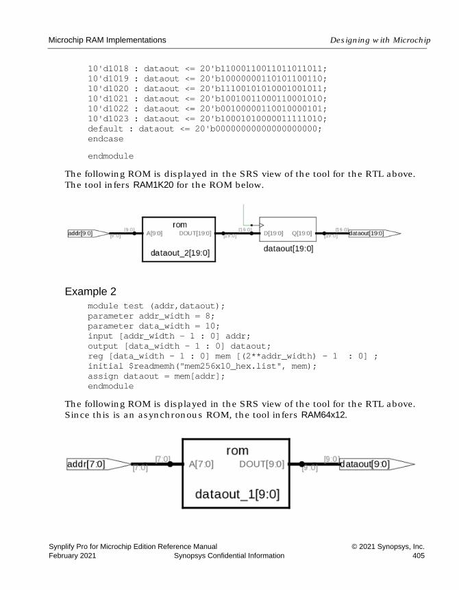
Microchip RAM Implementations Designing with Microchip
Synplify Pro for Microchip Edition Reference Manual © 2021 Synopsys, Inc.February 2021 Synopsys Confidential Information 405
10'd1018 : dataout <= 20'b11000110011011011011;10'd1019 : dataout <= 20'b10000000110101100110;10'd1020 : dataout <= 20'b11100101010001001011;10'd1021 : dataout <= 20'b10010011000110001010;10'd1022 : dataout <= 20'b00100000110010000101;10'd1023 : dataout <= 20'b10001010000011111010;default : dataout <= 20'b00000000000000000000;endcaseendmodule
The following ROM is displayed in the SRS view of the tool for the RTL above. The tool infers RAM1K20 for the ROM below.
Example 2module test (addr,dataout);parameter addr_width = 8;parameter data_width = 10;input [addr_width - 1 : 0] addr;output [data_width - 1 : 0] dataout;reg [data_width - 1 : 0] mem [(2**addr_width) - 1 : 0] ;initial $readmemh("mem256x10_hex.list", mem);assign dataout = mem[addr];endmodule
The following ROM is displayed in the SRS view of the tool for the RTL above. Since this is an asynchronous ROM, the tool infers RAM64x12.

LO
Designing with Microchip Microchip RAM Implementations
© 2021 Synopsys, Inc. Synplify Pro for Microchip Edition Reference Manual406 Synopsys Confidential Information February 2021
Write Byte-Enable Support for RAMFor RAM with n write enables used to control writing of data into memory locations, the compiler creates n sub-instances of the RAM with different write enables. The mapper merges these multiple RAM blocks into single or multiple block RAM, depending on the threshold and number of write enables. The write byte-enable pin (A_WEN/B_WEN [1:0]) of the block RAM primitives are configured to control the write operation for block RAMs.
Examplemodule ram (din, dout, addra, addrb, clk, wen1, wen2); input [7:0] din; input wen1;input wen2;input [9:0] addra; input clk; output reg [7:0] dout; localparam max_depth=1024; localparam min_width=8; reg [9:0] taddra;reg [min_width-1:0] mem_ram[max_depth-1:0]; always @(posedge clk) begin
taddra<=addra;if(wen1) mem_ram[taddra][3:0]<=din[3:0];
if(wen2) mem_ram[taddra][7:4]<=din[7:4];
end always @(posedge clk) begin
dout <= mem_ram[taddra];end endmodule
The compiler infers two ram1 shown in the SRS view below, which can be combined and mapped into a single RAM1K18_RT or RAM1K20.
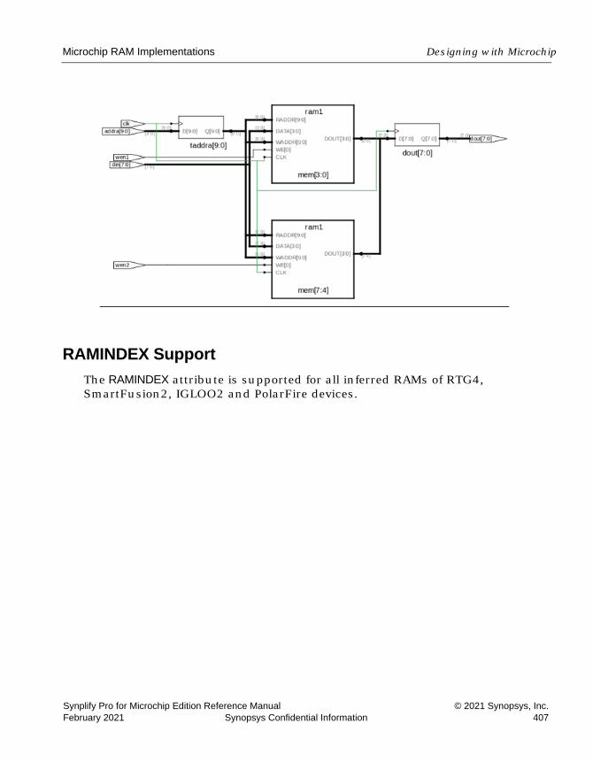
Microchip RAM Implementations Designing with Microchip
Synplify Pro for Microchip Edition Reference Manual © 2021 Synopsys, Inc.February 2021 Synopsys Confidential Information 407
RAMINDEX SupportThe RAMINDEX attribute is supported for all inferred RAMs of RTG4, SmartFusion2, IGLOO2 and PolarFire devices.

LO
Designing with Microchip Microchip Constraints and Attributes
© 2021 Synopsys, Inc. Synplify Pro for Microchip Edition Reference Manual408 Synopsys Confidential Information February 2021
Microchip Constraints and Attributes The synthesis tools let you specify timing constraints, general HDL attributes, and Microchip-specific attributes to improve your design. You can manage the attributes and constraints in the SCOPE interface. The following topics explain how to implement constraints and attributes for Microchip designs. Refer to:
• Global Buffer Promotion, on page 408
• The syn_maxfan Attribute in Microchip Designs, on page 409
• Radiation-tolerant Applications, on page 410
Global Buffer PromotionPolarFire, RTG4, SmartFusion2, IGLOO2 Technologies
The synthesis software inserts the global buffer (CLKINT) on clock, asynchro-nous set/reset, and data nets based on a threshold value. The supported devices have specific threshold values that cannot be changed for the different types of nets in the design. Inserting global buffers on nets with fanout greater than the threshold can help reduce the route delay during place and route.
Net Global buffer inserted for threshold value > or =
PolarFire Devices
Clock 2
Asynchronous Set/Reset 6
Data 5000
RTG4 Devices
Clock 2
Asynchronous Set/Reset 200000
Data 5000
SmartFusion2 and IGLOO2 Devices
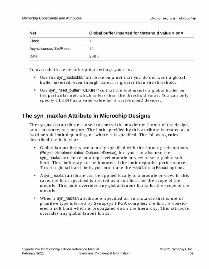
Microchip Constraints and Attributes Designing with Microchip
Synplify Pro for Microchip Edition Reference Manual © 2021 Synopsys, Inc.February 2021 Synopsys Confidential Information 409
To override these default option settings you can:
• Use the syn_noclockbuf attribute on a net that you do not want a global buffer inserted, even though fanout is greater than the threshold.
• Use syn_insert_buffer="CLKINT" so that the tool inserts a global buffer on the particular net, which is less than the threshold value. You can only specify CLKINT as a valid value for SmartFusion2 devices.
The syn_maxfan Attribute in Microchip DesignsThe syn_maxfan attribute is used to control the maximum fanout of the design, or an instance, net, or port. The limit specified by this attribute is treated as a hard or soft limit depending on where it is specified. The following rules described the behavior:
• Global fanout limits are usually specified with the fanout guide options (Project->Implementation Options->Device), but you can also use the syn_maxfan attribute on a top-level module or view to set a global soft limit. This limit may not be honored if the limit degrades performance. To set a global hard limit, you must use the Hard Limit to Fanout option.
• A syn_maxfan attribute can be applied locally to a module or view. In this case, the limit specified is treated as a soft limit for the scope of the module. This limit overrides any global fanout limits for the scope of the module.
• When a syn_maxfan attribute is specified on an instance that is not of primitive type inferred by Synopsys FPGA compiler, the limit is consid-ered a soft limit which is propagated down the hierarchy. This attribute overrides any global fanout limits.
Clock 2
Asynchronous Set/Reset 12
Data 5000
Net Global buffer inserted for threshold value > or =

LO
Designing with Microchip Microchip Constraints and Attributes
© 2021 Synopsys, Inc. Synplify Pro for Microchip Edition Reference Manual410 Synopsys Confidential Information February 2021
• When a syn_maxfan attribute is specified on a port, net, or register (or any primitive instance), the limit is considered a hard limit. This attribute overrides any other global fanout limits. Note that the syn_maxfan attri-bute does not prevent the instance from being optimized away and that design rule violations resulting from buffering or replication are the responsibility of the user.
Radiation-tolerant ApplicationsYou can specify the radiation-resistant design technique to use on an object for a design with the syn_radhardlevel attribute. This attribute can be applied to a module/architecture or a register output signal (inferred register in VHDL), and is used in conjunction with the Microchip macro files supplied with the software.
Values for syn_radhardlevel are as follows:
For details, see:
• Working with Microchip Radhard Designs, on page 542
• syn_radhardlevel, on page 195
Value Description
none Standard design techniques are used.
cc Combinational cells with feedback are used to implement storage rather than flip-flop or latch primitives.
tmr Triple module redundancy or triple voting is used to implement registers. Each register is implemented by three flip-flops or latches that “vote” to determine the state of the register.TMR reporting is supported for the PolarFire family. Local TMR of the register is reported in a file named *_tmr.rpt.
tmr_cc Triple module redundancy is used where each voting register is composed of combinational cells with feedback rather than flip-flop or latch primitives.
Microchip Device Mapping Options Designing with Microchip
Synplify Pro for Microchip Edition Reference Manual © 2021 Synopsys, Inc.February 2021 Synopsys Confidential Information 411
Microchip Device Mapping OptionsTo achieve optimal design results, set the correct implementation options. Some options include the following:
• Promote Global Buffer Threshold, on page 411
• I/O Insertion, on page 412
• Update Compile Point Timing Data Option, on page 413
• Operating Condition Device Option, on page 414
See Also• Microchip set_option Command Options, on page 417
• Microchip Tcl set_option Command Options, on page 418
Promote Global Buffer ThresholdThe Promote Global Buffer Threshold option is used for both ports and nets.
The Tcl command equivalent is set_option -globalthreshold value, where the value refers to the minimum number of fanout loads. The default value is 1.
Only signals with fanout loads larger than the defined value are promoted to global signals. The synthesis tool assigns the available global buffers to drive these signals using the following priority:
1. Clock
2. Asynchronous set/reset signal
3. Enable, data
SmartFusion2, IGLOO2, and RTG4 Global Buffer PromotionThe synthesis software inserts the global buffer (CLKINT) on clock, asynchro-nous set/reset, and data nets based on a threshold value. SmartFusion2, IGLOO2, and RTG4 devices have specific threshold values that cannot be changed for the different types of nets in the design. Inserting global buffers on nets with fanout greater than the threshold can help reduce the route delay during place and route.
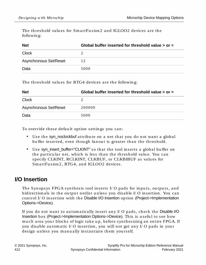
LO
Designing with Microchip Microchip Device Mapping Options
© 2021 Synopsys, Inc. Synplify Pro for Microchip Edition Reference Manual412 Synopsys Confidential Information February 2021
The threshold values for SmartFusion2 and IGLOO2 devices are the following:
The threshold values for RTG4 devices are the following:
To override these default option settings you can:
• Use the syn_noclockbuf attribute on a net that you do not want a global buffer inserted, even though fanout is greater than the threshold.
• Use syn_insert_buffer="CLKINT" so that the tool inserts a global buffer on the particular net, which is less than the threshold value. You can specify CLKINT, RCLKINT, CLKBUF, or CLKBIBUF as values for SmartFusion2, RTG4, and IGLOO2 devices.
I/O Insertion The Synopsys FPGA synthesis tool inserts I/O pads for inputs, outputs, and bidirectionals in the output netlist unless you disable I/O insertion. You can control I/O insertion with the Disable I/O Insertion option (Project->Implementation Options->Device).
If you do not want to automatically insert any I/O pads, check the Disable I/O Insertion box (Project->Implementation Options->Device). This is useful to see how much area your blocks of logic take up, before synthesizing an entire FPGA. If you disable automatic I/O insertion, you will not get any I/O pads in your design unless you manually instantiate them yourself.
Net Global buffer inserted for threshold value > or =
Clock 2
Asynchronous Set/Reset 12
Data 5000
Net Global buffer inserted for threshold value > or =
Clock 2
Asynchronous Set/Reset 200000
Data 5000
Microchip Device Mapping Options Designing with Microchip
Synplify Pro for Microchip Edition Reference Manual © 2021 Synopsys, Inc.February 2021 Synopsys Confidential Information 413
If you disable I/O insertion, you can instantiate the Microchip I/O pads you need directly. If you manually insert I/O pads, you only insert them for the pins that require them.
Update Compile Point Timing Data OptionPolarFire, SmartFusion2, IGLOO2Technologies
The Update Compile Point Timing Data option used with the Synopsys FPGA compile-point synthesis flow lets you break down a design into smaller synthesis units, called compile points, making incremental synthesis possible. See Synthesizing Compile Points, on page 455 in the User Guide.
The Update Compile Point Timing Data option controls whether or not changes to a locked compile point force remapping of its parents, taking into account the new timing model of the child.
Note: To simplify this description, the term child is used here to refer to a compile point that is contained inside another; the term parent is used to refer to the compile point that contains the child. These terms are thus not used here in their strict sense of direct, immediate containment: If a compile point A is nested in B, which is nested in C, then A and B are both considered children of C, and C is a parent of both A and B. The top level is consid-ered the parent of all compile points.
DisabledWhen the Update Compile Point Timing Data option is disabled (the default), only (locked) compile points that have changed are remapped, and their remap-ping does not take into account changes in the timing models of any of their children. The old (pre-change) timing model of a child is used, instead, to map and optimize its parents.
An exceptional case occurs when the option is disabled and the interface of a locked compile point is changed. Such a change requires that the immediate parent of the compile point be changed accordingly, so both are remapped. In this exceptional case, however, the updated timing model (not the old model) of the child is used when remapping this parent.
LO
Designing with Microchip Microchip Device Mapping Options
© 2021 Synopsys, Inc. Synplify Pro for Microchip Edition Reference Manual414 Synopsys Confidential Information February 2021
EnabledWhen the Update Compile Point Timing Data option is enabled, locked compile-point changes are taken into account by updating the timing model of the compile point and resynthesizing all of its parents (at all levels), using the updated model. This includes any compile point changes that took place prior to enabling this option, and which have not yet been taken into account (because the option was disabled).
The timing model of a compile point is updated when either of the following is true:
• The compile point is remapped, and the Update Compile Point Timing Data option is enabled.
• The interface of the compile point is changed.
Automatic Compile PointsPolarFire Technology
This feature is enabled, by default, only for PolarFire devices.
The tool supports the Automatic Compile Points (ACP) flow. For details, see The Automatic Compile Point Flow, on page 456 in the User Guide.
Operating Condition Device OptionYou can specify an operating condition for certain Microchip technologies:
• PolarFire
• RTG4
• SmartFusion2
• IGLOO2
Different operating conditions cause differences in device performance. The operating condition affects the following:
• optimization, if you have timing constraints
• timing analysis
• timing reports

Microchip Device Mapping Options Designing with Microchip
Synplify Pro for Microchip Edition Reference Manual © 2021 Synopsys, Inc.February 2021 Synopsys Confidential Information 415
To set an operating condition, select the value for Operating Conditions from the menu on the Device tab of the Implementation Options dialog box.
To set an operating condition in a project or Tcl file, use the command:
set_option -opcond value
where value can be specified like the following typical operating conditions:
Default Typical timing
MIL-WC Worst-case Military timing
MIL-TC Typical-case Military timing
MIL-BC Best-case Military timing
Automotive-WC Worst-case Automotive timing
LO
Designing with Microchip Microchip Device Mapping Options
© 2021 Synopsys, Inc. Synplify Pro for Microchip Edition Reference Manual416 Synopsys Confidential Information February 2021
For Example
The Microchip operating condition can contain any of the following specifica-tions:
• MIL—military
• COM—commercial
• IND—Industrial
• TGrade1
• TGrade2
as well as, include one of the following designations:
• WC—worst case
• BC—best case
• TC—typical case
For specific operating condition values for your required technology, see the Device tab on the Implementation Options dialog box.
Even when a particular operating condition is valid for a family, it may not be applicable to every part/package/speed-grade combination in that family. Consult Microchip's documentation or software for information on valid combinations and more information on the meaning of each operating condi-tion.

Microchip Device Mapping Options Designing with Microchip
Synplify Pro for Microchip Edition Reference Manual © 2021 Synopsys, Inc.February 2021 Synopsys Confidential Information 417
Microchip set_option Command OptionsTo select device mapping options for Microchip technologies, select Project -> Implementation Options->Device and set the options.
Option For details, see ...
Automatic Read/Write Check Insertion for RAM
Enabling this option automatically inserts bypass logic when required to prevent simulation mismatch in read-during-write scenarios. For asynchronous clocks, the tool will not generate bypass logic which can cause unintended CDC paths between the clocks. For more information about using this option in conjunction with the syn_ramstyle attribute, see syn_ramstyle , on page 199.
Conservative Register Optimization See the Microchip Tcl set_option Command Options , on page 418 for more information about the preserve_registers option.
Disable I/O Insertion I/O Insertion , on page 412.
Fanout Guide Setting Fanout Limits , on page 418 of the User Guide and The syn_maxfan Attribute in Microchip Designs, on page 409.
Operating Conditions (certain technologies) Operating Condition Device Option , on page 414
Promote Global Buffer Threshold Controlling Buffering and Replication , on page 420 of the User Guide and Promote Global Buffer Threshold , on page 411.
Resolve Mixed Drivers When a net is driven by a VCC or GND and active drivers, enable this option to connect the net to the VCC or GND driver.
Update Compile point Timing Data Update Compile Point Timing Data Option , on page 413

LO
Designing with Microchip Microchip Device Mapping Options
© 2021 Synopsys, Inc. Synplify Pro for Microchip Edition Reference Manual418 Synopsys Confidential Information February 2021
Microchip Tcl set_option Command OptionsYou can use the set_option Tcl command to specify the same device mapping options as are available through the Implementation Options dialog box displayed in the Project view with Project -> Implementation Options (see Implementation Options Command, on page 346).
This section describes the Microchip-specific set_option Tcl command options. These include the target technology, device architecture, and synthesis styles.
The table below provides information on specific options for Microchip archi-tectures. For a complete list of options for this command, refer to set_option, on page 113. You cannot specify a package (-package option) for some Micro-chip technologies in the synthesis tool environment. You must use the Micro-chip back-end tool for this.
.
Option Description
-technology keyword Sets target technology for the implementation. Keyword must be one of the following Microchip architecture names:IGLOO2, SmartFusion2, RTG4, PolarFire
-part partName Specifies a part for the implementation. Refer to the Implementation Options dialog box for available choices.
-package packageName RTG4 and PolarFire familiesSpecifies the package. Refer to Project-> Implementation Options->Device for available choices.
-speed_grade value Sets speed grade for the implementation. Refer to the Implementation Options dialog box for available choices.
-disable_io_insertion 1|0 Prevents (1) or allows (0) insertion of I/O pads during synthesis. The default value is false (enable I/0 pad insertion). For additional information about disabling I/O pads, see I/O Insertion , on page 412.

Microchip Device Mapping Options Designing with Microchip
Synplify Pro for Microchip Edition Reference Manual © 2021 Synopsys, Inc.February 2021 Synopsys Confidential Information 419
-fanout_limit value Sets fanout limit guidelines for the current project. For more information about fanout limits, see The syn_maxfan Attribute in Microchip Designs , on page 409.
-globalthreshold value PolarFire, SmartFusion2, IGLOO2, RTG4Sets fanout threshold for synchronous set/reset and data nets to infer CLKINT. Default value is 5000. For more information, see Promote Global Buffer Threshold , on page 411.
-clock_globalthreshold value PolarFire, SmartFusion2, IGLOO2, RTG4Sets fanout threshold for clock nets to infer CLKINT. Default value is 2.
-async_globalthreshold value Sets fanout threshold for asynchronous reset/set nets to infer CLKINT. Default value is 8 for RTG4 and 800 for PolarFire, SmartFusion2 and IGLOO2.
-opcond value PolarFire, IGLOO2Sets operating condition for device performance in the areas of optimization, timing analysis, and timing reports. Values are Default, MIL-WC, IND-WC, COM-WC, and Automotive-WC. See Operating Condition Device Option , on page 414 for more information.
-preserve_registers 1|0 When enabled, the software uses less restrictive register optimizations during synthesis if area is not as great a concern for your device. The default for this option is disabled (0).
-resolve_multiple_driver 1|0
When a net is driven by a VCC or GND and active drivers, enable this option to connect the net to the VCC or GND driver.
Option Description

LO
Designing with Microchip Microchip Device Mapping Options
© 2021 Synopsys, Inc. Synplify Pro for Microchip Edition Reference Manual420 Synopsys Confidential Information February 2021
-rw_check_on_ram 1 | 0 Enabling this option automatically inserts bypass logic when required, to prevent simulation mismatch in read-during-write scenarios. For asynchronous clocks, the tool will not generate bypass logic which can cause unintended CDC paths between the clocks.For more information about using this option in conjunction with the syn_ramstyle attribute, see syn_ramstyle , on page 199.
-update_models_cp 1|0 PolarFire, IGLOO2When set to 1, the locked compile point changes are taken into account, by updating the timing model of the compile point and resynthesizing all of its parents (at all levels), using the updated model. See Update Compile Point Timing Data Option , on page 413, for details.
-low_power_ram_decomp 0 |1 PolarFire, SmartFusion2, IGLOO2, RTG4Enables use of BLK pins of the RAM for reducing power consumption, by fracturing wide RAMs on the address width. Default value is 0.
-seqshift_to_uram 0 |1 PolarFire, SmartFusion2, IGLOO2, RTG4Enables inference of URAM if the threshold is met. Default value is 1.
-disable_ramindex 0 |1 PolarFire, SmartFusion2, IGLOO2, RTG4Disables the generation of RAMINDEX for RAM blocks if set to 1.
Option Description

Microchip Device Mapping Options Designing with Microchip
Synplify Pro for Microchip Edition Reference Manual © 2021 Synopsys, Inc.February 2021 Synopsys Confidential Information 421
-microsemi_enhanced_flow 0 |1 PolarFire, SmartFusion2, IGLOO2, RTG4Enables advanced constraint writer flow and writes the forward annotation constraints in Libero enhanced constraints format, when the value is set to 1. The default is 1.
-rep_clkint_driver 0 |1 PolarFire, SmartFusion2, IGLOO2, RTG4Enables replication of the register driving a CLKINT as well as some other loads, for which the fanout threshold is not met. Default value is 1.
-ternary_adder_decomp value PolarFire, SmartFusion2, IGLOO2, RTG4Enables ternary adder implementation with the limit of the adder output width set by default to 66. Ternary adder implementation can be turned off by setting the value to 0.
-pack_uram_addr_reg {0/1} PolarFire, SmartFusion2, IGLOO2, RTG4Disables packing of read address register in URAM if the option is set to 0. Default value is 1.
-polarfire_ram_init {0/1} Disables RAM initialization for the PolarFire device, if the value is set to 0. Default value is 1.
-gclkint_threshold {} PolarFireSets threshold for GCLKINT inference fanout. Default value is 1000.
-rgclkint_threshold {} PolarFireSets threshold for RGCLKINT inference fanout. Default value is 100.
-gclk_resource_count {} PolarFireSets limit on GCLKINT and RGCLKINT inference. Default value is 24.
Option Description
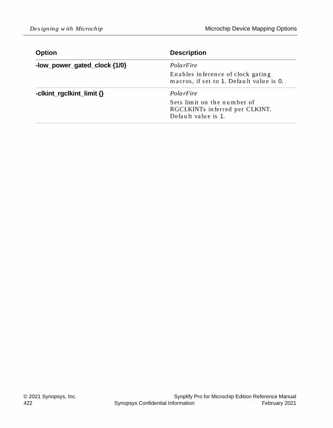
LO
Designing with Microchip Microchip Device Mapping Options
© 2021 Synopsys, Inc. Synplify Pro for Microchip Edition Reference Manual422 Synopsys Confidential Information February 2021
-low_power_gated_clock {1/0} PolarFireEnables inference of clock gating macros, if set to 1. Default value is 0.
-clkint_rgclkint_limit {} PolarFireSets limit on the number of RGCLKINTs inferred per CLKINT. Default value is 1.
Option Description
Microchip Output Files and Forward Annotation Designing with Microchip
Synplify Pro for Microchip Edition Reference Manual © 2021 Synopsys, Inc.February 2021 Synopsys Confidential Information 423
Microchip Output Files and Forward Annotation
The following procedures show you how to pass information or files that forward annotate information to the Microchip place-and-route tool. This section describes the following:
• VM Flow Support, on page 423
• Specifying Pin Locations, on page 424
• Specifying Locations for Microchip Bus Ports, on page 425
• Specifying Macro and Register Placement, on page 426
• Synthesis Reports, on page 426
After synthesis, the software generates a log file and output files for forward annotation to the Microchip P&R tool as described in some of the reports.
VM Flow SupportThe tool generates a Verilog output netlist (.vm) for the PolarFire, SmartFu-sion2, RTG4 and IGLOO2 devices for the P&R flow. After synthesis, the tool:
• Writes a separate SDC file (*_vm.sdc).
• Writes a separate TCL file (*_partition_vm.tcl) to forward annotate the timestamps on instances in an incremental compile point flow.
• Forward annotates properties like RTL attributes in the .vm netlist and constraints in an SDC file.
By default, the tool generates a .vm netlist. You can change the netlist from Verilog to EDIF.
The tool now supports the Libero Enhanced constraint flow by default. To disable this flow, the following switch needs to be added in the Synplify Pro project .prj file:
set_option -microchip_enhanced_flow 0To select a Verilog output netlist, go to Implementation Options->Implementation Results->Result Format. Select vm from the drop-down menu, click OK and save the project.

LO
Designing with Microchip Microchip Output Files and Forward Annotation
© 2021 Synopsys, Inc. Synplify Pro for Microchip Edition Reference Manual424 Synopsys Confidential Information February 2021
Specifying Pin LocationsIn certain technologies you can specify pin locations that are forward-annotated to the corresponding place-and-route tool. The following procedure shows you how to specify the appropriate attributes. For information about other placement properties, see Specifying Macro and Register Placement, on page 426.
1. Start with a design using an appropriate Microchip technology.
2. Add the appropriate attribute to the port. For a bus, list all the bus pins, separated by commas. To specify Microchip bus port locations, see Specifying Locations for Microchip Bus Ports, on page 425.
– To add the attribute from the SCOPE interface, click the Attributes tab and specify the appropriate attribute and value.

Microchip Output Files and Forward Annotation Designing with Microchip
Synplify Pro for Microchip Edition Reference Manual © 2021 Synopsys, Inc.February 2021 Synopsys Confidential Information 425
– To add the attribute in the source files, use the appropriate attribute and syntax. For details about the attributes in the tables, see the Attribute Reference Manual.
Specifying Locations for Microchip Bus Ports You can specify pin locations for Microchip bus ports. To assign pin numbers to a bus port, or to a single- or multiple-bit slice of a bus port, do the following:
1. Open the constraint file and add these attributes to the design.
2. Specify the syn_noarrayports attribute globally to bit blast all bus ports in the design.
define_global_attribute syn_noarrayports {1};3. Use the alspin attribute to specify pin locations for individual bus bits.
This example shows locations specified for individual bits of bus ADDRESS0.
define_attribute {ADDRESS0[4]} alspin {26}define_attribute {ADDRESS0[3]} alspin {30}define_attribute {ADDRESS0[2]} alspin {33}define_attribute {ADDRESS0[1]} alspin {38}define_attribute {ADDRESS0[0]} alspin {40}The software forward-annotates these pin locations to the place-and-route software.
Vendor Family Attribute and Value
Microchip syn_loc {pin_number}oralspin {pin_number}

LO
Designing with Microchip Microchip Output Files and Forward Annotation
© 2021 Synopsys, Inc. Synplify Pro for Microchip Edition Reference Manual426 Synopsys Confidential Information February 2021
Specifying Macro and Register Placement You can use attributes to specify macro and register placement in Microchip designs. The information here supplements the pin placement information described in Specifying Pin Locations, on page 424 and bus pin placement information described in Specifying Locations for Microchip Bus Ports, on page 425.
Synthesis Reports The synthesis tool generates a resource usage report, a timing report, and a net buffering report for the Microchip designs that you synthesize.To view the synthesis reports, click View Log.
For ... Use ...
Relative placement of Microchip macros and IP blocks
alsloc define_attribute {u1} alsloc {R15C6}
Integration with Microchip Tools and Flows Designing with Microchip
Synplify Pro for Microchip Edition Reference Manual © 2021 Synopsys, Inc.February 2021 Synopsys Confidential Information 427
Integration with Microchip Tools and FlowsThe following procedures provide Microchip-specific design tips.
• Compile Point Synthesis, on page 427
• Incremental Synthesis Flow, on page 428
• Using Predefined Microchip Black Boxes, on page 428
• Using Smartgen Macros, on page 429
• Microchip Place-and-Route Tools, on page 429
Compile Point SynthesisMicrochip PolarFire
Compile-point synthesis is available when you want to isolate portions of a design in order to stabilize results and/or improve runtime performance during placement and routing, the Synopsys FPGA The compile-point synthesis flow lets you achieve incremental design and synthesis without having to write and maintain sets of complex, error-prone scripts to direct synthesis and keep track of design dependencies. See Synthesizing Compile Points, on page 455 for a description, and Working with Compile Points, on page 435 in the User Guide for a step-by-step explanation of the compile-point synthesis flow.
In device technologies that can take advantage of compile points, you break down your design into smaller synthesis units or compile points, in order to make incremental synthesis possible. A compile point is a module that is treated as a block for incremental mapping: When your design is resynthe-sized, compile points that have already been synthesized are not resynthe-sized, unless you have changed:
• the HDL source code in such a way that the design logic is changed,
• the constraints applied to the compile points, or
• the device mapping options used in the design.
(For details on the conditions that necessitate resynthesis of a compile point, see Compile Point Basics, on page 436, and Update Compile Point Timing Data Option, on page 413.)
LO
Designing with Microchip Integration with Microchip Tools and Flows
© 2021 Synopsys, Inc. Synplify Pro for Microchip Edition Reference Manual428 Synopsys Confidential Information February 2021
Incremental Synthesis FlowMicrochip IGLOO2 and SmartFusion2 Technologies
The synthesis tool provides timestamps for each manual compile point in the *_partition.tcl file. You can use the timestamps to check whether the compile point was resynthesized in an incremental run of the tool.
To run this flow:
1. Define compile point constraint on the modules in the design. For example:
define_compile_point {viewName} -type {locked, partition} -cpfile {fileName}
2. Run the standard synthesis flow. The synthesis tool writes the timestamps for each compile point in the designName_partition.tcl file. For example:
set_partition_info -name partitionName -timestamp timestamp
For an incremental synthesis run, only affected compile points display new timestamps, while unaffected compile points retain the same timestamps.
Check the Compile Point Summary report available in the log file.
Using Predefined Microchip Black BoxesThe Microchip macro libraries contain predefined black boxes for Microchip macros so that you can manually instantiate them in your design. For infor-mation about using ACTGen macros, see Using Smartgen Macros, on page 429. For general information about working with black boxes, see Defining Black Boxes for Synthesis, on page 382.
To instantiate an Microchip macro, use the following procedure.
1. Locate the Microchip macro library file appropriate to your technology and language (v or vhd) in one of these subdirectories under installDirectory/lib.
Microchip Macros for Microchip technologies.

Integration with Microchip Tools and Flows Designing with Microchip
Synplify Pro for Microchip Edition Reference Manual © 2021 Synopsys, Inc.February 2021 Synopsys Confidential Information 429
Use the macro file that corresponds to your target architecture.
2. Add the Microchip macro library at the top of the source file list for your synthesis project. Make sure that the library file is first in the list.
3. For VHDL, also add the appropriate library and use clauses to the top of the files that instantiate the macros:
library family;use family.components.all;
Specify the appropriate technology in family.
Using Smartgen MacrosThe Smartgen macros replace the ACTgen macros, which were available in the previous Designer 6.x place-and-route tool. The following procedure shows you how to include Smartgen macros in your design. For information about using Microchip macro libraries, see Using Predefined Microchip Black Boxes, on page 428. For general information about working with black boxes, see Defining Black Boxes for Synthesis, on page 382.
1. In Smartgen, generate the function you want to include.
2. For Verilog macros, do the following:
– Include the appropriate Microchip macro library file for your target architecture in your the source files list for your project.
– Include the Verilog version of the Smartgen result in your source file list. Make sure that the Microchip macro library is first in the source files list, followed by the Smartgen Verilog files, followed by the other source files.
3. Synthesize your design as usual.
Microchip Place-and-Route ToolsYou can run place and route automatically after synthesis. For details on how to set options, see Running P&R Automatically after Synthesis, on page 554 in the User Guide.
For details about the place-and-route tools, refer to the Microchip documen-tation.
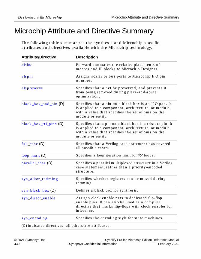
LO
Designing with Microchip Microchip Attribute and Directive Summary
© 2021 Synopsys, Inc. Synplify Pro for Microchip Edition Reference Manual430 Synopsys Confidential Information February 2021
Microchip Attribute and Directive SummaryThe following table summarizes the synthesis and Microchip-specific attributes and directives available with the Microchip technology.
Attribute/Directive Description
alsloc Forward annotates the relative placements of macros and IP blocks to Microchip Designer.
alspin Assigns scalar or bus ports to Microchip I/O pin numbers.
alspreserve Specifies that a net be preserved, and prevents it from being removed during place-and-route optimization.
black_box_pad_pin (D) Specifies that a pin on a black box is an I/O pad. It is applied to a component, architecture, or module, with a value that specifies the set of pins on the module or entity.
black_box_tri_pins (D) Specifies that a pin on a black box is a tristate pin. It is applied to a component, architecture, or module, with a value that specifies the set of pins on the module or entity.
full_case (D) Specifies that a Verilog case statement has covered all possible cases.
loop_limit (D) Specifies a loop iteration limit for for loops.
parallel_case (D) Specifies a parallel multiplexed structure in a Verilog case statement, rather than a priority-encoded structure.
syn_allow_retiming Specifies whether registers can be moved during retiming.
syn_black_box (D) Defines a black box for synthesis.
syn_direct_enable Assigns clock enable nets to dedicated flip-flop enable pins. It can also be used as a compiler directive that marks flip-flops with clock enables for inference.
syn_encoding Specifies the encoding style for state machines.
(D) indicates directives; all others are attributes.

Microchip Attribute and Directive Summary Designing with Microchip
Synplify Pro for Microchip Edition Reference Manual © 2021 Synopsys, Inc.February 2021 Synopsys Confidential Information 431
syn_enum_encoding (D) Specifies the encoding style for enumerated types (VHDL only).
syn_hier Controls the handling of hierarchy boundaries of a module or component during optimization and mapping.
syn_insert_buffer Inserts a clock buffer according to the specified value.
syn_insert_pad Removes an existing I/O buffer from a port or net when I/O buffer insertion is enabled.
syn_isclock (D) Specifies that a black-box input port is a clock, even if the name does not indicate it is one.
syn_keep (D) Prevents the internal signal from being removed during synthesis and optimization.
syn_looplimit Specifies a loop iteration limit for while loops in the design.
syn_maxfan Overrides the default fanout guide for an individual input port, net, or register output.
syn_multstyle Determines how multipliers are implemented for Microchip devices.
syn_netlist_hierarchy Determines whether the EDIF output netlist is flat or hierarchical.
syn_noarrayports Prevents the ports in the EDIF output netlist from being grouped into arrays, and leaves them as individual signals.
syn_noclockbuf Turns off the automatic insertion of clock buffers.
syn_noprune (D) Controls the automatic removal of instances that have outputs that are not driven.
syn_no_compile_point Use this attribute with the Automatic Compile Point (ACP) feature. If you do not want the software to create a compile point for a particular view or module, then apply this attribute.
syn_pad_type Specifies an I/O buffer standard.
Attribute/Directive Description
(D) indicates directives; all others are attributes.

LO
Designing with Microchip Microchip Attribute and Directive Summary
© 2021 Synopsys, Inc. Synplify Pro for Microchip Edition Reference Manual432 Synopsys Confidential Information February 2021
syn_preserve (D) Prevents sequential optimizations across a flip-flop boundary during optimization, and preserves the signal.
syn_probe Adds probe points for testing and debugging.
syn_radhardlevel Specifies the radiation-resistant design technique to apply to a module, architecture, or register.
syn_ramstyle Specifies the implementation to use for an inferred RAM. You apply syn_ramstyle globally, to a module, or to a RAM instance.
syn_reference_clock Specifies a clock frequency other than that implied by the signal on the clock pin of the register.
syn_replicate Controls replication.
syn_resources Specifies resources used in black boxes.
syn_safe_case Enables/disables the safe case option. When enabled, the high reliability safe case option turns off sequential optimizations for counters, FSM, and sequential logic to increase the circuit’s reliability.
syn_sharing (D) Specifies resource sharing of operators.
syn_shift_resetphase Allows you to remove the flip-flop on the inactive clock edge, built by the reset recovery logic for an FSM when a single event upset (SEU) fault occurs.
syn_state_machine (D) Determines if the FSM Compiler extracts a structure as a state machine.
syn_tco<n> (D) Defines timing clock to output delay through the black box. The n indicates a value between 1 and 10.
syn_tpd<n> (D) Specifies timing propagation for combinational delay through the black box. The n indicates a value between 1 and 10.
syn_tristate (D) Specifies that a black-box pin is a tristate pin.
Attribute/Directive Description
(D) indicates directives; all others are attributes.

Microchip Attribute and Directive Summary Designing with Microchip
Synplify Pro for Microchip Edition Reference Manual © 2021 Synopsys, Inc.February 2021 Synopsys Confidential Information 433
syn_tsu<n> (D) Specifies the timing setup delay for input pins, relative to the clock. The n indicates a value between 1 and 10.
syn_useenables Generates clock enable pins for registers.
translate_off/translate_on (D)
Specifies sections of code to exclude from synthesis, such as simulation-specific code.
Attribute/Directive Description
(D) indicates directives; all others are attributes.

LO
Designing with Microchip Microchip Attribute and Directive Summary
© 2021 Synopsys, Inc. Synplify Pro for Microchip Edition Reference Manual434 Synopsys Confidential Information February 2021
Synplify Pro for Microchip Edition Reference Manual © 2021 Synopsys, Inc.February 2021 Synopsys Confidential Information 435
Index
Symbols_ta.srm file 155.adc file 144.areasrr file 152.fse file 152.info file 152.ini file 144.prj file 144.sap
annotated properties for analyst 154.sar file 154.sdc file 144.srd file 154.srm file 154.srr file 157
watching selected information 37.srs file 155
initial values (Verilog) 235.sv file 145
SystemVerilog source file 145.ta file
See timing report file 155.v file 145.vhd file 145.vhm file 157.vm file 157
AACTgen macros 429adc file (analysis design constraint) 144adder
SYNCore 334adders
SYNCore 335Allow Docking command 38
alspinbus port pin numbers 425
Alt key, selecting columns in Text Editor 47
analysis design constraint file (.adc) 144Analyst toolbar 59annotated properties for analyst
.sap 154
.timing annotated properties (.tap) 156archive file (.sar) 154areasrr file
hierarchical area report 172arrow keys, selecting objects in
Hierarchy Browser 109arrow pointers for push and pop 108asynchronous clock report
description 170attributes
inferring RAM 184attributes (Microchip) 430Attributes demo 50auto constraints 141
Maximize option 74
Bblack boxes
See also macros, macro librariesMicrochip 379
block RAMdual-port RAM examples 200inferring 187modes 183NO_CHANGE mode example 196READ_FIRST mode example 195single-port RAM examples 197types 183WRITE_FIRST mode example 193
block RAMs
© 2021 Synopsys, Inc. Synplify Pro for Microchip Edition Reference Manual436 Synopsys Confidential Information February 2021
syn_ramstyle attribute 432buttons and options, Project view 72byte-enable RAMs
SYNCore 304
Ccck.rpt file (constraint checking report)
152check boxes, Project view 72clock buffering report, log file (.srr) 159clock groups
Clock Relationships (timing report) 168clock pin drivers, selecting all 82clock relationships, timing report 168clock report
asynchronous 162Clock Tree, HDL Analyst tool 82clocks
asynchronous report 170declared clock 164defining 82derived clock 165inferred clock 164system clock 165
color codingText Editor 47
commenting out code (Text Editor) 47compile points
Microchip 427updating data (Microchip) 413
compiler report, log file (.srr) 158Constraint Check command 173constraint checking report 173constraint files 125
.sdc 144automatic. See auto constraintsfdc and sdc precedence order 128
constraint files (.sdc)creating 58
constraint priority 128constraints
auto constraints. See auto constraintsnon-DC 135priority 128
report file 173styles 127types 124
context help editor 48context of filtered schematic, displaying
114context sensitive help
using the F1 key 18copying
for pasting 65counter compiler
SYNCore 358counters
SYNCore 359critical paths 119
analyzing 120finding 120
cross-clock paths, timing analysis 168cross-hair mouse pointer 55crossprobing 99
definition 99Ctrl key
avoiding docking 57multiple selection 54zooming using the mouse wheel 56
cutting (for pasting) 58
Ddeclared clock 164deleting
See removingderived clock 165design size, schematic sheet
setting 102device options (Microchip) 417directives (Microchip) 430Dissolve Instances command 117docking 38
avoiding 57docking GUI entities
toolbar 57DSP blocks
inferencing 381

Synplify Pro for Microchip Edition Reference Manual © 2021 Synopsys, Inc.February 2021 Synopsys Confidential Information 437
dual-port RAM examples 200dual-port RAMs
SYNCore parameters 287
Eeditor view
context help 48encoding
state machineFSM Explorer 74
examplesInteractive Attribute Examples 50
Explorer, FSMenabling 74
Ffailures, timing (definition) 121fanout
Microchip 409fdc
constraint priority 128precedence over sdc 128
fdc constraints 130generation process 128
fdc filerelationship with other constraint files
125feature comparison
FPGA tools 14FIFO compiler
SYNCore 250FIFO flags
empty/almost empty 272full/almost full 271handshaking 272programmable 274programmable empty 277programmable full 275
FIFOscompiling with SYNCore 251
files.adc 144.areasrr 152.fdc 144.fse 152
.info 152
.ini 144
.prj 144
.sar 154
.sdc 144
.srm 154, 155
.srr 157watching selected information 37
.srs 155
.ta 155
.v 145
.vhd 145
.vhm 157
.vm 157compiler output (.srs) 155constraint (.adc) 144constraint (.sdc) 144creating 58customized timing report (.ta) 155design component info (.info) 152initialization (.ini) 144log (.srr) 157
watching selected information 37mapper output (.srm) 154, 155output
See output filesproject (.prj) 144RTL view (.srs) 155srr 157
watching selected information 37state machine encoding (.fse) 152Synopsys archive file (.sar) 154synthesis output 152Technology view (.srm) 154, 155Verilog (.v) 145VHDL (.vhd) 145
files for synthesis 144filtered schematic
compared with unfiltered 85filtering 113
commands 113compared with flattening 117FSM states and transitions 85paths from pins or ports 121
filtering critical paths 120finding
critical paths 120information on synthesis tool 19
GUI 18

© 2021 Synopsys, Inc. Synplify Pro for Microchip Edition Reference Manual438 Synopsys Confidential Information February 2021
finite state machinesSee state machines
Flatten Current Schematic command 117Flatten Schematic command 117flattening
commands 115compared with filtering 117selected instances 116
Float commandWatch window popup menu 38
floatingtoolbar 57
floating toolbar popup menu 57forward annotation
initial values 235Forward Annotation of Initial Values
Verilog 235frequency
cross-clock paths 168Frequency (Mhz) option, Project view 73fse file 152FSM Compiler option, Project view 74FSM Compiler, enabling and disabling
globallywith GUI 74
FSM encoding file (.fse) 152FSM Explorer
enabling 74FSM Explorer option, Project view 74FSM toolbar 62FSM Viewer 83FSMs (finite state machines)
See state machines
Ggeneric technology library 149graphical user interface (GUI), overview
21GTECH library. See generic technology
librarygtech.v library 149gui
synthesis software 17
GUI (graphical user interface), overview 21
HHDL Analyst tool 77
accessing commands 86analyzing critical paths 119Clock Tree 82crossprobing 99filtering designs 113finding objects 97hierarchical instances. See hierarchical
instancesobject information 88preferences 102push/pop mode 105ROM table viewer 243schematic sheet size 102schematics, filtering 113schematics, multiple-sheet 102status bar information 88title bar information 102
HDL Analyst toolbarSee Analyst toolbar
HDL Analyst views 78See also RTL view, Technology view
HDL files, creating 58header, timing report 163help
onlineaccessing 18
hidden hierarchical instances 93are not flattened 117
Hide commandfloating toolbar popup menu 57Log Watch window popup menu 38Tcl Window popup menu 41
hierarchical area report 172.areasrr file 172
hierarchical instances 91compared with primitive 90display in HDL Analyst 91hidden 93opaque 91transparent 91
hierarchical schematic sheet, definition 102

Synplify Pro for Microchip Edition Reference Manual © 2021 Synopsys, Inc.February 2021 Synopsys Confidential Information 439
hierarchyflattening
compared with filtering 117pushing and popping 105schematic sheets 102
Hierarchy Browser 109changing size in view 78Clock Tree 82finding schematic objects 97moving between objects 82RTL view 78symbols (legend) 83Technology view 80trees of objects 82
II/O insertion (Microchip) 412Identify Instrumentor
launching 63IEEE 1364 Verilog 95 standard 146Implementation Directory 32Implementation Results 32indenting a block of text 47indenting text (Text Editor) 47inferencing
DSP blocks 381inferred clock 164info file (design component info) 152ini file 144initial value data file
Verilog 232Initial Values
forward annotation 235initial values
$readmemb 229$readmemh 229
initial values (Verilog)netlist file (.srs) 235
initialization file (.ini) 144input files 144
.adc 144
.ini 144
.sdc 144
.sv 145
.v 145
.vhd 145inserting
bookmarks (Text Editor) 47instances
hierarchicaldissolving 110making transparent 110
hierarchical. See hierarchical instancesprimitive. See primitive instances
Interactive Attribute Examples 50interface information, timing report 169IPs
SYNCore byte-enable RAMs 304SYNCore counters 359SYNCore FIFOs 251SYNCore RAMs 281SYNCore ROMs 321SYNCore subtractors 335
isolating paths from pins or ports 121
Kkeyboard shortcuts 64
arrow keys (Hierarchy Browser) 109keyword completion, Text Editor 47keywords
completing in Text Editor 47
Llatches
in timing analysis 119Launch Identify Instrumentor icon 63legacy sdc file. See sdc files, difference
between legacy and Synopsys standard
lib2synusing 150
librariesgeneral technology 148macro, built-in 145technology-independent 148VHDL
attributes and constraints 146linkerlog file 153log file (.srr) 157
watching selected information 37

© 2021 Synopsys, Inc. Synplify Pro for Microchip Edition Reference Manual440 Synopsys Confidential Information February 2021
log file report 157clock buffering 159compiler 158mapper 159net buffering 159resource usage 160retiming 161summary of compile points 160timing 160
Log Watch Configuration dialog box 39Log Watch window 37
Output Windows 45positioning commands 38
Mmacros
libraries 145Microchip 379SIMBUF 380
mapper output file (.srm) 154, 155mapper report
log file (.srr) 159margin, slack 120message viewer
description 41Messages Tab 41Microchip
ACTgen macros 429attributes 430black boxes 379compile point synthesis 427compile point timing data 413device options 417directives 430features 376I/O insertion 412macro libraries 428macros 379Operating Condition Device Option 414output netlist 375pin numbers for bus ports 425product families 374reports 426SIMBUF macro 380Tcl implementation options 418
Microchip implementing RAM 388mouse button operations 54
mouse operations 52Mouse Stroke Tutor 53mouse wheel operations 56Move command
floating toolbar window 57Log Watch window popup menu 38Tcl window popup menu 41
moving between objects in the Hierarchy Browser 82
moving GUI entitiestoolbar 57
multiple-sheet schematics 102multipliers
DSP blocks 381multisheet schematics
transparent hierarchical instances 104
Nnavigating
among hierarchical levelsby pushing and popping 105with the Hierarchy Browser 109
among the sheets of a schematic 102nesting design details (display) 110net buffering report, log file 159netlist file 157
initial values (Verilog) 235netlists for different vendors 375
Oobject information
status bar, HDL Analyst tool 88viewing in HDL Analyst tool 88
objectscrossprobing 99dissolving 110making transparent 110
objects, schematicSee schematic objects
Online helpF1 key 18
online helpaccessing 18
opaque hierarchical instances 91
Synplify Pro for Microchip Edition Reference Manual © 2021 Synopsys, Inc.February 2021 Synopsys Confidential Information 441
are not flattened 117options
Project view 72Frequency (Mhz) 73FSM Compiler 74FSM Explorer 74Resource Sharing 75Retiming 75
options (Microchip) 418output files 152
.areasrr 152
.info 152
.sar 154
.srm 154, 155
.srr 157watching selected information 37
.srs 155
.ta 155
.vhm 157
.vm 157netlist 157See also files
Output Windows 45Overview of the Synopsys FPGA
Synthesis Tools 12
Pparameters
SYNCore adder/subtractor 343SYNCore byte-enable RAM 311SYNCore counter 365SYNCore FIFO 256SYNCore RAM 289SYNCore ROM 326
partitioning of schematics into sheets 102
pasting 58performance summary, timing report 163pins
displayingon transparent instances 95
displaying on technology-specific primitives 96
isolating paths from 121pointers, mouse
cross-hairs 55push/pop arrows 108
popping up design hierarchy 105popup menus
floating toolbar 57Log Watch window 38, 39Log Watch window positioning 38Tcl window 41
precedence of constraint files 128preferences
HDL Analyst tool 102primitive instances 90primitives
pin names in Technology view 96prj file 144Process View 33project files (.prj) 144project results
Implementation Directory 32Process View 33Project Status View 26
Project Results View 26Project Status View 26Project toolbar 57Project view 22
buttons and options 72options 72Synplify Pro 22
Project window 22project_name_cck.rpt file 173push/pop mode, HDL Analyst tool 105
RRAM implementations
Microchip 388RAM inference 183
using attributes 184RAMs
compiling with SYNCore 281inferring block RAM 187initial values (Verilog) 229SYNCore 281SYNCore, byte-enable 304
RAMs, inferringadvantages 182

© 2021 Synopsys, Inc. Synplify Pro for Microchip Edition Reference Manual442 Synopsys Confidential Information February 2021
reference manual, role in document set 11
removingbookmark (Text Editor) 47window (view) 57
reportsconstraint checking (cck.rpt) 173hierarchical area report 172
Resource Sharing option, Project view 75resource usage report, log file 160retiming
report, log file 161Retiming option, Project view 75ROM compiler
SYNCore 319ROM inference examples 243ROM initialization
with rom.info file 246with Verilog generate block 247
rom.info file 243ROMs
SYNCore 321RTL view 78
displaying 60file (.srs) 155
Sschematic objects
crossprobing 99definition 88dissolving 110finding 97making transparent 110status bar information 88
schematic sheets 102hierarchical (definition) 102navigating among 102setting size 102
schematicsconfiguring amount of logic on a sheet
102crossprobing 99filtered 85filtering commands 113flattening compared with filtering 117flattening selectively 116
hierarchical (definition) 102multiple-sheet 102multiple-sheet. See also schematic
sheetsobject information 88partitioning into sheets 102sheet connectors 89sheets
navigating among 102size, setting 102
size in view, changing 78unfiltered 85unfiltering 114
SCOPEfor legacy sdc 132
sdcfdc precedence 128SCOPE for legacy files 132
sdc filedifference between legacy and
Synopsys standard 127sdc2fdc utility 133selecting
text column (Text Editor) 47selecting multiple objects using the Ctrl
key 54set_rtl_ff_names 135sheet connectors 89Shift key 57shortcuts
keyboardSee keyboard shortcuts
SIMBUF macro 380single-port RAM examples 197single-port RAMs
SYNCore parameters 286slack
cross-clock paths 169defined 164margin
definition 121setting 120
source filesSee also filescreating 58
srd file 154

Synplify Pro for Microchip Edition Reference Manual © 2021 Synopsys, Inc.February 2021 Synopsys Confidential Information 443
srm file 154, 155srr file 157
watching selected information 37srs file 155
initial values (Verilog) 235standards, supported
Verilog 146VHDL 146
state machinesencoding
displaying 85FSM Explorer 74
encoding file (.fse) 152filtering states and transitions 85state encoding, displaying 85
status bar information, HDL Analyst tool 88
structural netlist file (.vhm) 157structural netlist file (.vm) 157subtractor
SYNCore 334subtractors
SYNCore 335summary of compile points report
log file (.srr) 160supported standards
Verilog 146VHDL 146
symbolsHierarchy Browser (legend) 83
syn_maxfanfanout limits (Microchip) 409
syn_noarrayports attributeuse with alspin 425
SYNCoreadder/subtractor 334adder/subtractor parameters 343adders 335byte-enable RAM compiler
byte-enable RAM compilerSYNCore 303
byte-enable RAM parameters 311counter compiler 358counter parameters 365counters 359FIFO compiler 250, 251
FIFO parameters 256RAM compiler
RAM compilerSYNCore 281
RAM parameters 289RAMs 281RAMs, byte-enable 304RAMs, dual-port parameters 287RAMs, single-port parameters 286ROM compiler 319ROM parameters 326ROMs 321ROMs, parameters 325subtractors 335
SYNCore adder/subtractoradders 346dynamic adder/subtractor 352functional description 334subtractors 349
SYNCore FIFOsdefinition 250parameter definitions 269port list 266read operations 266status flags 271write operations 265
SYNCore ROMsdual-port read 331parameter list 331single-port read 330
Synopsys FPGA Synthesis Toolsoverview 12
Synopsys standard sdc file. See sdc files, difference between legacy and Synopsys standard
Synplify Pro toolProject view 22user interface 17
Synplify tooluser interface 17
synthesislog file (.srr) 157
watching selected information 37synthesis software
gui 17system clock 165SystemVerilog keywords
context help 48
© 2021 Synopsys, Inc. Synplify Pro for Microchip Edition Reference Manual444 Synopsys Confidential Information February 2021
Tta file (customized timing report) 155Tcl commands
constraint files 131pasting 41
Tcl Script windowOutput Windows 45
Tcl shell commandsdc2fdc 133
Tcl windowpopup menu commands 41popup menus 41
Technology view 80displaying 60file (.srm) 154, 155
Text Editorfeatures 47indenting a block of text 47opening 46selecting text column 47view 45
text editorcompleting keywords 47
Text Editor view 45timing analysis of critical paths (HDL
Analyst tool) 119timing analyst
cross-clock paths 168timing annotated properties (.tap) 156timing constraints
See also FPGA timing constraintsSee constraints
timing failures, definition 121timing report 162
clock relationships 168customized (.ta file) 155file (.ta) 155header 163interface information 169performance summary 163
timing reportsasynchronous clocks 170log file (.srr) 160
title bar information, HDL Analyst tool 102
toolbars 57FSM 62moving and docking 57
transparent hierarchical instances 92lower-level logic on multiple sheets 104operations resulting in 112pins and pin names 95
trees of objects, Hierarchy Browser 82trees, browser, collapsing and expanding
82
Uunfiltered schematic, compared with
filtered 85unfiltering schematic 114user interface
Synplify Pro tool 17user interface, overview 21using the mouse 52utilities
lib2syn 150sdc2fdc 133
Vv file 145vendor technologies
Microchip 373vendor-specific netlists 375Verilog
Forward Annotation of Initial Values 235
generic technology library 149initial value data file 232initial values for RAMs 229Microchip ACTgen macros 429netlist file 157ROM inference 243source files (.v) 145structural netlist file (.vm) 157supported standards 146
Verilog 2001 146Verilog 95 146Verilog macro libraries
Microchip 428
Synplify Pro for Microchip Edition Reference Manual © 2021 Synopsys, Inc.February 2021 Synopsys Confidential Information 445
Verilog source file (.v) 145vhd file 145vhd source file 145VHDL
librariesattributes, supplied with synthesis
tool 146macro libraries, Microchip 428source files (.vhd) 145structural netlist file (.vhm) 157supported standards 146
VHDL source file (.vhd) 145vhm file 157views 36
FSM 83Project 22removing 57RTL 78Technology 80
vm file 157
WWatch Window. See Log Watch windowwindow
Project 22windows 36
closing 66log watch 37removing 57
Zzoom
using the mouse wheel and Ctrl key 56

LO
© 2021 Synopsys, Inc. Synplify Pro for Microchip Edition Reference Manual446 Synopsys Confidential Information February 2021


