Synthesis and applications of graphene electrodesDolly Shin1,2, Sukang Bae1, Chao Yan1,3, Junmo Kang1, Jaechul Ryu1, Jong-Hyun Ahn1,3,♠ and Byung Hee Hong1,2,♠
1Center for Human Interface Nano Technology (HINT) and SKKU Advanced Institute of Nanotechnology (SAINT), Sungkyunkwan University, Suwon 440-746, Korea2Department of Chemistry, Seoul National University, Seoul 151-747, Korea3School of Advanced Materials Science and Engineering, Sungkyunkwan University, Suwon 440-746, Korea
Received 1 September 2011Accepted 18 December 2011
AbstractThe near explosion of attention given to graphene has attracted many to its research field. As new studies and findings about graphene synthesis, properties, electronic quality control, and pos-sible applications simultaneous burgeon in the scientific community, it is quite hard to grasp the breadth of graphene history. At this stage, graphene’s many fascinating qualities have been amply reported and its potential for various electronic applications are increasing, pulling in ever more newcomers to the field of graphene. Thus it has become important as a community to have an equal understanding of how this material was discovered, why it is stirring up the scientific com-munity and what sort of progress has been made and for what purposes. Since the first discovery, the hype has expediently led to near accomplishment of industrial-sized production of graphene. This review covers the progress and development of synthesis and transfer techniques with an emphasis on the most recent technique of chemical vapor deposition, and explores the potential applications of graphene that are made possible with the improved synthesis and transfer.
Key words: graphene, graphene synthesis, graphene applications, overview of graphene research development
1. Why Graphene?
With countless numbers of scientific journals and patents spewing out each year, graphene has received undivided attention from the scientific and engineering applications commu-nities, ever since the experimental confirmation of its existence. The discovery of the two dimensional, single atom layer-thick graphite with well-ordered honeycomb crystal lattice has shattered the previous arguments made by Peierls [1], Landau [2], Geim and Novoselov [3] that two-dimensional (2D) materials are thermodynamically unstable and cannot exist in a free state. Such a paradigm shift was already a tremendous attention gatherer. With the fortuitous discovery of single layer graphene, other 2D crystals were also discovered soon after [2,4,5]. Nevertheless, what made graphene the superstar of 2D crystalline materials are the unusual electrical and physical properties and the seemingly innumerable possibilities of new applications that may be brought forth by such properties. Some of the characteristics that excite scholars of graphene are its high intrinsic carrier mobility (200 000 cm2v-1s-1) [6,7], high thermal conductivity (~5000 Wm-1K-1) [8], high Young’s modulus (~1.0 TPa) [9], and high optical transmittance (~97.7%) [10], just to name a few.
The theoretical ground of graphene has been studied for 70 years [1,2] and it was already predicted that the charge carriers of two dimensional graphene sheet would behave like a massless Dirac fermion rather than follow the Schrodinger equation, which successfully di-rects most other materials’ quantum properties [3]. But up until Novoselov et al. [4,5] proved the existence of such a material, graphene was all but a theoretical model.
DOI: http://dx.doi.org/ 10.5714/CL.2012.13.1.001
This is an Open Access article distributed under the terms of the Creative Commons Attribution Non-Commercial License (http://creativecommons.org/licenses/by-nc/3.0/) which permits unrestricted non-commercial use, distribution, and reproduction in any medium, provided the original work is properly cited.
Synthesis and applications of graphene electrodesDolly Shin, Sukang Bae, Chao Yan, Junmo Kang, Jaechul Ryu, Jong-Hyun Ahn and Byung Hee Hong
Graphene eld-eect transistor for radio-frequency applications : review Jeong-Sun Moon
Issues with the electrical characterization of graphene devicesByoung Hun Lee, Young Gon Lee, Uk Jin Jung, Yong Hun Kim, Hyeon Jun Hwang, Jin Ju Kim and Chang Goo Kang
KCS Korean Carbon Society
carbonlett.org
REVIEWS
pISSN: 1976-4251 eISSN: 2233-4998VOL. 13 NO. 1 January 31 2012
Carbon Letters Vol. 13, No. 1, 1-16 (2012)
DOI: http://dx.doi.org/10.5714/CL.2012.13.1.001 2
increases with the increasing gate voltage from both sides of the resistivity peak. Interestingly, the device did not show a zero-
2. The Breakthrough Technique
The first discovery, or the first synthesis method, of gra-phene came from a rather simple technique. This method, mi-cromechanical exfoliation of highly oriented pyrolytic graphite (HOPG), involves repeatedly pulling apart graphite flakes into progressively thinner layers with Scotch tape until a few layers of graphene are obtained and placed onto silica wafers. The lat-eral size of such graphene can be up to 10 μm (Fig. 1) [4].
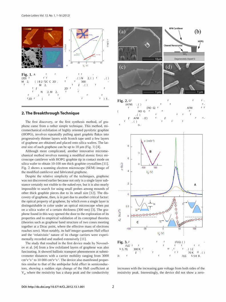
Although more complicated, another innovative microme-chanical method involves running a modified atomic force mi-croscope cantilever with HOPG graphite tip in contact mode on silica wafer to obtain 10-100 nm thick graphite crystallites [11]. Fig. 2 shows a scanning electron microscope (SEM) image of the modified cantilever and fabricated graphene.
Despite the relative simplicity of the techniques, graphene was not discovered earlier because not only is a single layer sub-stance certainly not visible to the naked eye, but it is also nearly impossible to search for using small probes among mounds of other thick graphite pieces due to its small size [12]. The dis-covery of graphene, then, is in part due to another critical factor: the optical property of graphene, by which even a single layer is distinguishable in color under an optical microscope when put on a silica wafer of a certain thickness (300 nm) [3]. The gra-phene found in this way opened the door to the exploration of its properties and to empirical validation of its conceptual theories (theories such as graphene band structure of two cones meeting together at a Dirac point, where the effective mass of electrons reaches zero). Most notably, its half integer quantum Hall effect and the ‘relativistic’ nature of its charge carriers were experi-mentally recorded and studied extensively [11].
The study that resulted in the first device made by Novosel-ov et al. [4] from a few exfoliated layers of graphene was also fascinating. It showed ballistic transport phenomenon at submi-crometer distances with a carrier mobility ranging from 3000 cm2v-1s-1 to 10 000 cm2v-1s-1. The device also manifested proper-ties similar to that of the ambipolar field effect in semiconduc-tors, showing a sudden sign change of the Hall coefficient at Vg, where the resistivity has a sharp peak and the conductivity
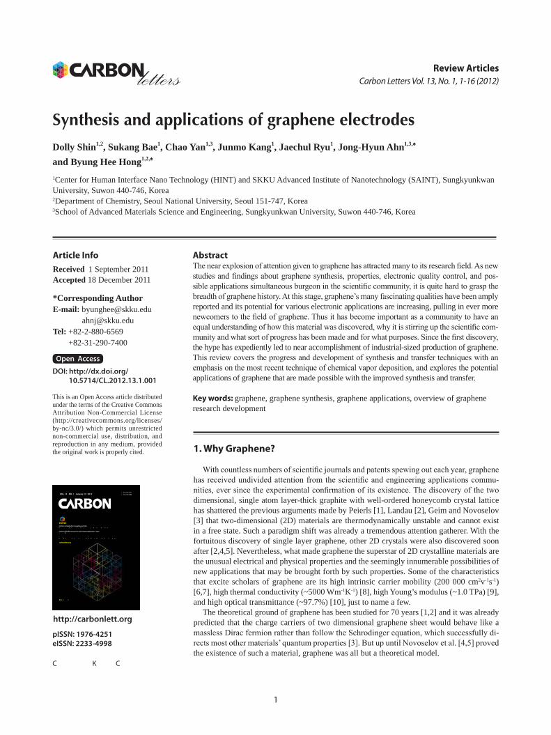
Fig. 1. Atomic force microscope images of various two-dimensional (2D) crystals discovered along with graphene. (a) NbSe2, (b) graphite, (c) MoS2, and (d) Bi2Sr2CaCu2Ox. The crystals are on 300 nm oxidized Si wa-fer except the MoS2, which is on holey carbon lm. (e) The graph shows the electric eld eect in sheets of 2D crystals. The changes in electrical conductivity of NbSe2, MoS2, and graphene are shown as a function of gate voltage. It is clear that graphene has a distinct trend compared to other 2D crystals (inset is the device used to measure the conductivity) [5]. Fig. 2. Graphene micromechanical cleaving using atomic force micro-
scope (AFM) tip. (a) Scanning electron microscope image of highly ori-ented pyrolytic graphite (HOPG) crystallite mounted on an AFM cantilever (inset is the bulk HOPG surface patterned by masked anisotropic oxygen plasma etching. (b) schematic drawing of the microleaving process using the modied AFM tip. (C) thin graphite lms obtained by the microcleav-ing process. (d) a mesoscoping device fabricated from the obtained graphite sample [6].
Fig. 3. Field eect in a few layers of grapheme (FLG). (a) Relationship be-tween FLG’s resistivity change and gate voltage for dierent temperatures at T = 5, 70, and 300 K, from top to bottom curves, respectively. (b) Example of changes in the lm’s conductivity obtained by inverting the 70 K curve. (c) Hall coecient as a function of gate voltage for the same FLG at T = 5 K [4].
Overview of graphene synthesis and applications
3 http://carbonlett.org
the graphite to create puffed graphite layers in an effort to create a scalable production method of single layer graphene.
Despite the relative ease with which reduced GO can be made, the quality of the graphene sheets that are made is not so high. Because small suspended graphene particles are dispersed onto a substrate, the substrate does not have an orderly crystal structure or uniform thickness. Graphene provided by micro-mechanical exfoliation from HOPG still provides better quality graphene with a well-preserved crystalline structure. Thus the efforts to improve graphene synthesis continue.
3.2. Epitaxial growth on SiC
As a more scalable approach was sought, and epitaxial grow-ing of graphene by thermal decomposition of SiC received at-tention. Epitaxial growth of thin films on crystalline structures has been around for a long time [20-22]. Even before free standing graphene was obtained from the exfoliation method, surface science has driven the growth of single crystalline (but not truly monolayer or free standing), homogeneous growth of epitaxial graphite layers, as opposed to HOPG graphene, which has a polycrystalline structure resulting from in-plane azimuthal disorder [23-25]. As the optimization for epitaxial single layer graphene growth became feasible, several transfer methods ap-peared afterwards, making it possible to obtain free standing epitaxial graphene on desired substrates.
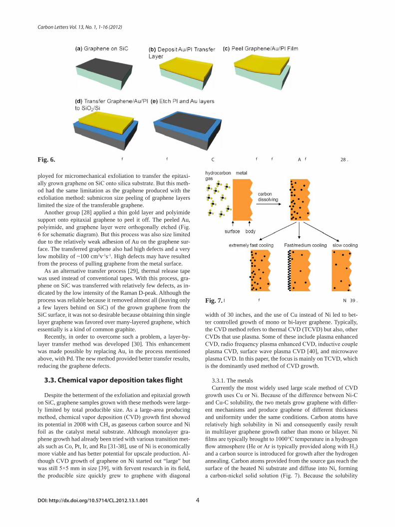
Analysis of experimental results from low-energy electron diffraction (LEED), grazing incidence X-ray diffraction, and scanning tunneling microscopy confirmed the highly ordered, single crystalline structure and relatively smooth and flat sur-face of epitaxially grown graphite on SiC (Fig. 5) [20-22,26]. The study opened the possibility of growing macroscopic sized growths of single graphene planes.
Work by Berger et al. [26] reported that several layer graphite grown under ultra-high vacuum (UHV) condition at temperatures of 1250-1450°C on Si-terminated face of single-crystal 6H-SiC exhibited measured electron mobility of about 1100 cm2v-1s-1, which is an acceptable value for some electronics applications.
Initially, Lee et al. [27] used a procedure similar to that em-
conductance region but rather intrinsically exhibited an interme-diate state at which the device was a mixture of holes and elec-tron conductors (Fig. 3). As an attractive quality of a graphene device, its electronic characteristics can be tuned by applying a varying gate voltage, changing the device from purely electron or hole conductor to mixed hole-electron conductor.
3. Road to Mass Production
As seen from the few discovered examples of compelling electronic properties of graphene, exfoliation from HOPG pro-vides graphene with the quality and size that satisfy the needs of scientific research. With such needs met, many of the suc-ceeding synthesis efforts were geared toward producing larger, uniform, and mass-producible graphene sheet in the hopes of meeting the commercial need for graphene in various applica-tions in the future.
3.1. Chemical exfoliation
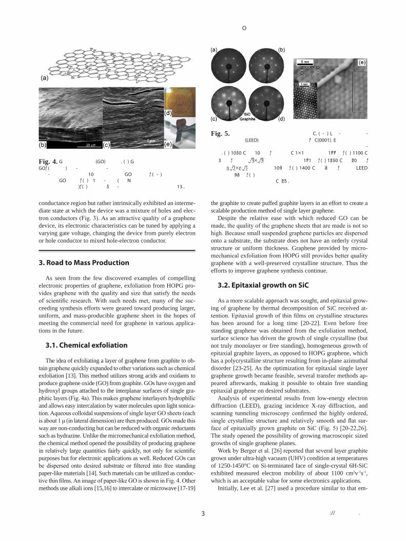
The idea of exfoliating a layer of graphene from graphite to ob-tain graphene quickly expanded to other variations such as chemical exfoliation [13]. This method utilizes strong acids and oxidants to produce graphene oxide (GO) from graphite. GOs have oxygen and hydroxyl groups attached to the interplanar surfaces of single gra-phitic layers (Fig. 4a). This makes graphene interlayers hydrophilic and allows easy intercalation by water molecules upon light sonica-tion. Aqueous colloidal suspensions of single layer GO sheets (each is about 1 μ (in lateral dimension) are then produced. GOs made this way are non-conducting but can be reduced with organic reductants such as hydrazine. Unlike the micromechanical exfoliation method, the chemical method opened the possibility of producing graphene in relatively large quantities fairly quickly, not only for scientific purposes but for electronic applications as well. Reduced GOs can be dispersed onto desired substrate or filtered into free standing paper-like materials [14]. Such materials can be utilized as conduc-tive thin films. An image of paper-like GO is shown in Fig. 4. Other methods use alkali ions [15,16] to intercalate or microwave [17-19]
Fig. 4. Graphene oxide (GO) sheets. (a) General chemical structure of GO; (b and c) low- and medium-resolution scanning electron microscope side-view images of ~10 micron thick GO sample; (d-f ) digital camera image of GO paper; (d) ~1 μm-thick (the Northwestern University logo is beneath the paper); (e) folded ~5 μm-thick semitransparent lm [13].
Fig. 5. Thin graphite grown epitaxially on SiC. (a-d) Low-energy elec-tron diraction (LEED) patterns from graphite/SiC(0001). Each represents sample that was heated several times to successively higher tempera-tures. (a) 1050°C for 10 min; shows SiC 1×1 pattern at 177 eV; (b) 1100°C for 3 min; shows × reconstruction at 171 eV; (c) 1250°C for 20 min; shows × pattern at 109 eV; (c) 1400°C for 8 min; shows LEED pattern at 98 eV; (e) scanning tunneling microscopy image of a surface region of graphite grown on SiC [26].
Carbon Letters Vol. 13, No. 1, 1-16 (2012)
DOI: http://dx.doi.org/10.5714/CL.2012.13.1.001 4
width of 30 inches, and the use of Cu instead of Ni led to bet-ter controlled growth of mono or bi-layer graphene. Typically, the CVD method refers to thermal CVD (TCVD) but also, other CVDs that use plasma. Some of these include plasma enhanced CVD, radio frequency plasma enhanced CVD, inductive couple plasma CVD, surface wave plasma CVD [40], and microwave plasma CVD. In this paper, the focus is mainly on TCVD, which is the dominantly used method of CVD growth.
3.3.1. The metalsCurrently the most widely used large scale method of CVD
growth uses Cu or Ni. Because of the difference between Ni-C and Cu-C solubility, the two metals grow graphene with differ-ent mechanisms and produce graphene of different thickness and uniformity under the same conditions. Carbon atoms have relatively high solubility in Ni and consequently easily result in multilayer graphene growth rather than mono or bilayer. Ni films are typically brought to 1000°C temperature in a hydrogen flow atmosphere (He or Ar is typically provided along with H2) and a carbon source is introduced for growth after the hydrogen annealing. Carbon atoms provided from the source gas reach the surface of the heated Ni substrate and diffuse into Ni, forming a carbon-nickel solid solution (Fig. 7). Because the solubility
ployed for micromechanical exfoliation to transfer the epitaxi-ally grown graphene on SiC onto silica substrate. But this meth-od had the same limitation as the graphene produced with the exfoliation method: submicron size peeling of graphene layers limited the size of the transferable graphene.
Another group [28] applied a thin gold layer and polyimide support onto epitaxial graphene to peel it off. The peeled Au, polyimide, and graphene layer were orthogonally etched (Fig. 6 for schematic diagram). But this process was also size limited due to the relatively weak adhesion of Au on the graphene sur-face. The transferred graphene also had high defects and a very low mobility of ~100 cm2v-1s-1. High defects may have resulted from the process of pulling graphene from the metal surface.
As an alternative transfer process [29], thermal release tape was used instead of conventional tapes. With this process, gra-phene on SiC was transferred with relatively few defects, as in-dicated by the low intensity of the Raman D-peak. Although the process was reliable because it removed almost all (leaving only a few layers behind on SiC) of the grown graphene from the SiC surface, it was not so desirable because obtaining thin single layer graphene was favored over many-layered graphene, which essentially is a kind of common graphite.
Recently, in order to overcome such a problem, a layer-by-layer transfer method was developed [30]. This enhancement was made possible by replacing Au, in the process mentioned above, with Pd. The new method provided better transfer results, reducing the graphene defects.
3.3. Chemical vapor deposition takes ight
Despite the betterment of the exfoliation and epitaxial growth on SiC, graphene samples grown with these methods were large-ly limited by total producible size. As a large-area producing method, chemical vapor deposition (CVD) growth first showed its potential in 2008 with CH4 as gaseous carbon source and Ni foil as the catalyst metal substrate. Although monolayer gra-phene growth had already been tried with various transition met-als such as Co, Pt, Ir, and Ru [31-38], use of Ni is economically more viable and has better potential for upscale production. Al-though CVD growth of graphene on Ni started out “large” but was still 5×5 mm in size [39], with fervent research in its field, the producible size quickly grew to graphene with diagonal
Fig. 6. Schematic illustration of the steps for transferring graphene grown on an SiC wafer to another substrate by using the Au peeling method [28].
Fig. 7. Illustration of carbon segregation at metal surface such as Ni [39].
Overview of graphene synthesis and applications
5 http://carbonlett.org
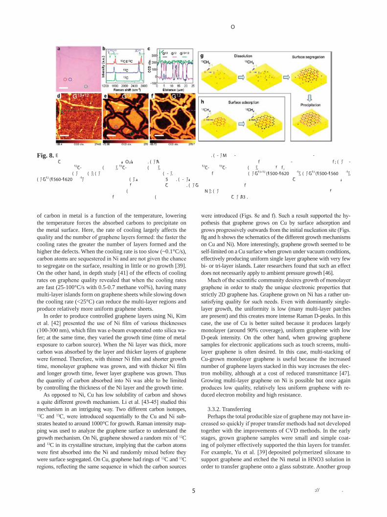
were introduced (Figs. 8e and f). Such a result supported the hy-pothesis that graphene grows on Cu by surface adsorption and grows progressively outwards from the initial nucleation site (Figs. 8g and h shows the schematics of the different growth mechanisms on Cu and Ni). More interestingly, graphene growth seemed to be self-limited on a Cu surface when grown under vacuum conditions, effectively producing uniform single layer graphene with very few bi- or tri-layer islands. Later researchers found that such an effect does not necessarily apply to ambient pressure growth [46].
Much of the scientific community desires growth of monolayer graphene in order to study the unique electronic properties that strictly 2D graphene has. Graphene grown on Ni has a rather un-satisfying quality for such needs. Even with dominantly single-layer growth, the uniformity is low (many multi-layer patches are present) and this creates more intense Raman D-peaks. In this case, the use of Cu is better suited because it produces largely monolayer (around 90% coverage), uniform graphene with low D-peak intensity. On the other hand, when growing graphene samples for electronic applications such as touch screens, multi-layer graphene is often desired. In this case, multi-stacking of Cu-grown monolayer graphene is useful because the increased number of graphene layers stacked in this way increases the elec-tron mobility, although at a cost of reduced transmittance [47]. Growing multi-layer graphene on Ni is possible but once again produces low quality, relatively less uniform graphene with re-duced electron mobility and high resistance.
3.3.2. TransferringPerhaps the total producible size of graphene may not have in-
creased so quickly if proper transfer methods had not developed together with the improvements of CVD methods. In the early stages, grown graphene samples were small and simple coat-ing of polymer effectively supported the thin layers for transfer. For example, Yu et al. [39] deposited polymerized siloxane to support graphene and etched the Ni metal in HNO3 solution in order to transfer graphene onto a glass substrate. Another group
of carbon in metal is a function of the temperature, lowering the temperature forces the absorbed carbons to precipitate on the metal surface. Here, the rate of cooling largely affects the quality and the number of graphene layers formed: the faster the cooling rates the greater the number of layers formed and the higher the defects. When the cooling rate is too slow (~0.1°C/s), carbon atoms are sequestered in Ni and are not given the chance to segregate on the surface, resulting in little or no growth [39]. On the other hand, in depth study [41] of the effects of cooling rates on graphene quality revealed that when the cooling rates are fast (25-100°C/s with 0.5-0.7 methane vol%), having many multi-layer islands form on graphene sheets while slowing down the cooling rate (<25°C) can reduce the multi-layer regions and produce relatively more uniform graphene sheets.
In order to produce controlled graphene layers using Ni, Kim et al. [42] presented the use of Ni film of various thicknesses (100-300 nm), which film was e-beam evaporated onto silica wa-fer; at the same time, they varied the growth time (time of metal exposure to carbon source). When the Ni layer was thick, more carbon was absorbed by the layer and thicker layers of graphene were formed. Therefore, with thinner Ni film and shorter growth time, monolayer graphene was grown, and with thicker Ni film and longer growth time, fewer layer graphene was grown. Thus the quantity of carbon absorbed into Ni was able to be limited by controlling the thickness of the Ni layer and the growth time.
As opposed to Ni, Cu has low solubility of carbon and shows a quite different growth mechanism. Li et al. [43-45] studied this mechanism in an intriguing way. Two different carbon isotopes, 12C and 13C, were introduced sequentially to the Cu and Ni sub-strates heated to around 1000°C for growth. Raman intensity map-ping was used to analyze the graphene surface to understand the growth mechanism. On Ni, graphene showed a random mix of 12C and 13C in its crystalline structure, implying that the carbon atoms were first absorbed into the Ni and randomly mixed before they were surface segregated. On Cu, graphene had rings of 12C and 13C regions, reflecting the same sequence in which the carbon sources
Fig. 8. Exploration of graphene growth mechanisms using dierent carbon isotopes. (a-f ) Micro-Raman characterization of the isotope-labeled graphene grown on Cu foil and transferred onto an SiO2/Si wafer. (a) An optical micrograph of the identical region analyzed with micro-Raman spectroscopy; (b) Ra-man spectra from 12C-graphene (green), 13C-graphene (blue), and the junction of 12C- and 13C-graphene (red), respectively, marked with the corresponding colored circles in (a) and (e); (c) line scan of the dashed line in (d-f ). integrated intensity Raman maps of (d) G13+12 (1500-1620 cm-1), (e) G13 (1500-1560 cm-1), (f ) G12 (1560-1620 cm-1) of the areas shown in (a). Scale bars are 5 μm. (g-h) Schematic diagrams of the possible distribution of C isotopes in graphene lms based on dierent growth mechanisms for sequential input of C isotopes. (g) Graphene with randomly mixed carbon isotopes atoms such as might occur from surface segregation and precipitation (as expected for graphene growth on Ni); (h) graphene with carbon isotopes grown in the same sequence of input carbon source as might occur by surface adsorption (as expected for graphene growth on Cu) [43].
Carbon Letters Vol. 13, No. 1, 1-16 (2012)
DOI: http://dx.doi.org/10.5714/CL.2012.13.1.001 6
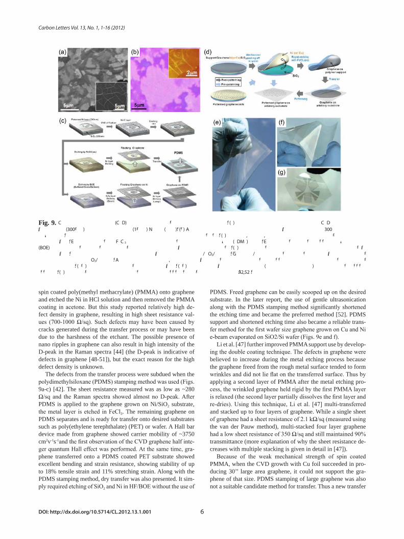
PDMS. Freed graphene can be easily scooped up on the desired substrate. In the later report, the use of gentle ultrasonication along with the PDMS stamping method significantly shortened the etching time and became the preferred method [52]. PDMS support and shortened etching time also became a reliable trans-fer method for the first wafer size graphene grown on Cu and Ni e-beam evaporated on SiO2/Si wafer (Figs. 9e and f).
Li et al. [47] further improved PMMA support use by develop-ing the double coating technique. The defects in graphene were believed to increase during the metal etching process because the graphene freed from the rough metal surface tended to form wrinkles and did not lie flat on the transferred surface. Thus by applying a second layer of PMMA after the metal etching pro-cess, the wrinkled graphene held rigid by the first PMMA layer is relaxed (the second layer partially dissolves the first layer and re-dries). Using this technique, Li et al. [47] multi-transferred and stacked up to four layers of graphene. While a single sheet of graphene had a sheet resistance of 2.1 kΩ/sq (measured using the van der Pauw method), multi-stacked four layer graphene had a low sheet resistance of 350 Ω/sq and still maintained 90% transmittance (more explanation of why the sheet resistance de-creases with multiple stacking is given in detail in [47]).
Because of the weak mechanical strength of spin coated PMMA, when the CVD growth with Cu foil succeeded in pro-ducing 30’’ large area graphene, it could not support the gra-phene of that size. PDMS stamping of large graphene was also not a suitable candidate method for transfer. Thus a new transfer
spin coated poly(methyl methacrylate) (PMMA) onto graphene and etched the Ni in HCl solution and then removed the PMMA coating in acetone. But this study reported relatively high de-fect density in graphene, resulting in high sheet resistance val-ues (700-1000 Ω/sq). Such defects may have been caused by cracks generated during the transfer process or may have been due to the harshness of the etchant. The possible presence of nano ripples in graphene can also result in high intensity of the D-peak in the Raman spectra [44] (the D-peak is indicative of defects in graphene [48-51]), but the exact reason for the high defect density is unknown.
The defects from the transfer process were subdued when the polydimethylsiloxane (PDMS) stamping method was used (Figs. 9a-c) [42]. The sheet resistance measured was as low as ~280 Ω/sq and the Raman spectra showed almost no D-peak. After PDMS is applied to the graphene grown on Ni/SiO2 substrate, the metal layer is etched in FeCl3. The remaining graphene on PDMS separates and is ready for transfer onto desired substrates such as poly(ethylene terephthalate) (PET) or wafer. A Hall bar device made from graphene showed carrier mobility of ~3750 cm2v-1s-1and the first observation of the CVD graphene half inte-ger quantum Hall effect was performed. At the same time, gra-phene transferred onto a PDMS coated PET substrate showed excellent bending and strain resistance, showing stability of up to 18% tensile strain and 11% stretching strain. Along with the PDMS stamping method, dry transfer was also presented. It sim-ply required etching of SiO2 and Ni in HF/BOE without the use of
Fig. 9. Chemical vapor deposition (CVD) graphene and wafer-scale synthesis and transfer. (a) Scanning electron microscope images of CVD grown graphene lms on thin (300-nm) nickel layers and thick (1-mm) Ni foils (inset). (b) An optical microscope image of the graphene lm transferred to a 300 nm thick silicon dioxide layer. The inset atomic force microscope image shows a typical rippled structure. (c) Synthesis, etching, and transfer process of the large-scale patterned graphene lms. Etching is done using FeCl3 and the transfer is done using polydimethylsiloxane (PDMS) stamp. Etching can be done using buered oxide etchant (BOE) or hydrogen uoride solution and dry-transfer of the graphene lms at room temperature. (d) Schematic illustration for fast etching and transfer of wafer-size graphene lms. Transferring and patterning of graphene lms grown on a metal/SiO2/Si wafer. Graphene/metal layers supported by polymer lms are mechani-cally separated from an SiO2/Si wafer. After fast etching of metal, the graphene lms can be transferred to arbitrary substrates and then patterned using conven-tional lithography. (e-g) Photographs of wafer-scale graphene lms. (e-f) The graphene lms printed on a poly(ethylene terephthalate) and a stretchable rubber substrate. (g) The three-element rosette strain gauge pattern on rubber by pre-patterning method [42,52].
Overview of graphene synthesis and applications
7 http://carbonlett.org
mechanism.In a sense, the desire to understand the growth mechanism
of graphene itself is in part fueled by the aspiration to produce large graphene sheets with few defects. The theoretical study of the thermodynamics of graphene growth [54] predicts that the existence of any of the hydrocarbon species provided by meth-ane (CH4, CH3, CH2, and CH are referred to as CHx from this point on) is unfavorable on the Cu surface. It was calculated that rather than existing as an individual CHx species on Cu, the hydrocarbon species are thermodynamically more stable and stay in clusters of CHx. The minimum size of this cluster of CHx that results in a lower energy level is the critical nucleation size of carbons for graphene formation. Starting from the nucleation sites, graphene islands (typically called domain or grain) grow in size until the islands meet and eventually cover the entire cat-alytic metal surface. Currently, the exact mechanism of how the switch from CHx clusters to graphene occurs is not understood. Nevertheless, the findings opened the possibility of controlling the nucleation sites and numbers.
In a recent study [44], experiments were carried out to find growth conditions that can decrease the number of nucleation sites. The results revealed that under high temperature and low pressure and methane flow conditions, fewer nucleation sites were formed compared to conditions of higher pressure and methane flow. The experiment also involved increasing the size of each graphene domain. This is of interest because when two different domain boundaries meet upon full growth, they cre-ate defects on graphene (resulting in high D-peak in the Raman spectra), which is believed to be responsible for the high sheet resistance and electron scattering. Under higher pressure (still less than ambient pressure) and high methane flow, each domain
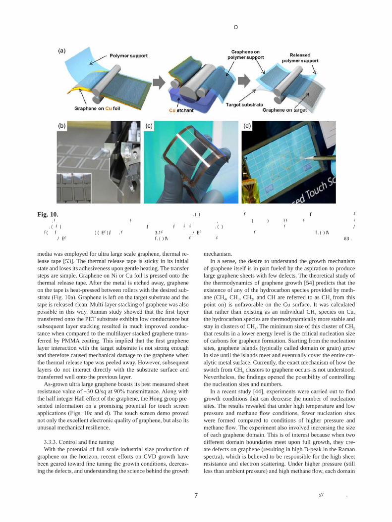
media was employed for ultra large scale graphene, thermal re-lease tape [53]. The thermal release tape is sticky in its initial state and loses its adhesiveness upon gentle heating. The transfer steps are simple. Graphene on Ni or Cu foil is pressed onto the thermal release tape. After the metal is etched away, graphene on the tape is heat-pressed between rollers with the desired sub-strate (Fig. 10a). Graphene is left on the target substrate and the tape is released clean. Multi-layer stacking of graphene was also possible in this way. Raman study showed that the first layer transferred onto the PET substrate exhibits low conductance but subsequent layer stacking resulted in much improved conduc-tance when compared to the multilayer stacked graphene trans-ferred by PMMA coating. This implied that the first graphene layer interaction with the target substrate is not strong enough and therefore caused mechanical damage to the graphene when the thermal release tape was peeled away. However, subsequent layers do not interact directly with the substrate surface and transferred well onto the previous layer.
As-grown ultra large graphene boasts its best measured sheet resistance value of ~30 Ω/sq at 90% transmittance. Along with the half integer Hall effect of the graphene, the Hong group pre-sented information on a promising potential for touch screen applications (Figs. 10c and d). The touch screen demo proved not only the excellent electronic quality of graphene, but also its unusual mechanical resilience.
3.3.3. Control and fine tuningWith the potential of full scale industrial size production of
graphene on the horizon, recent efforts on CVD growth have been geared toward fine tuning the growth conditions, decreas-ing the defects, and understanding the science behind the growth
Fig. 10. Roll to roll production of graphene and touch screen application. (a) Schematic of the roll-based production of graphene lms grown on a cop-per foil. The process includes adhesion of polymer support such as thermal release tape, copper etching (rinsing) and dry-transfer-printing on a target sub-strate. (b-d) Photographs of application of graphene lm grown by roll-to-roll method. (b) Screen printing process of silver paste electrodes on graphene/poly(ethylene terephthalate) (PET) lms. The inset shows 3.1-inch graphene/PET panels patterned with silver electrodes before assembly. (c) An assembled graphene/PET touch panel showing outstanding exibility. (f ) A graphene-based touch-screen panel connected to a computer with control software [53].
Carbon Letters Vol. 13, No. 1, 1-16 (2012)
DOI: http://dx.doi.org/10.5714/CL.2012.13.1.001 8
and also to higher concentration Cu vapor at static equilibrium. Raman spectroscopy confirmed the uniform monolayer growth and field-effect transistor measurements showed a high electron mobility of 4000 cm2v-1s-1
Another study that controlled graphene growth conditions [46] explored the effects of different pressure conditions on the layers of graphene formed on the Cu surface. The major finding of the study was that under ambient pressure, the growth result-ed in thick graphene layers and a non-uniform surface, especial-ly at high methane flow rate (lowering the flow rate somewhat increased the surface uniformity and decreased the layer thick-ness). Under low pressure and UHV conditions, typical growth was reproduced, creating nicely uniform, single-layer graphene. Thus, the previously reported self-limiting characteristic of gra-phene growth on Cu was found to be restricted to low pressure growth conditions.
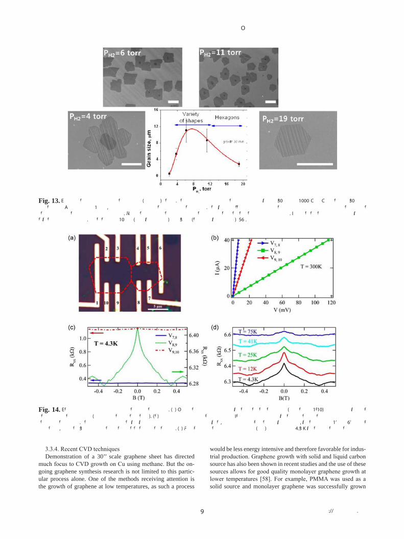
Lastly, one of the most recent notable findings is the identifi-cation of the role of hydrogen gas flow in CVD growth. Previ-ous journals presenting their CVD growth methods mention the use of hydrogen gas flow for the purpose of annealing the metal surface. Work by Vlassiouk et al. [56] revealed the surprisingly critical roles that hydrogen play in CVD growth. First, hydrogen appears to be a co-catalyst of the metal in producing graphene. Under low hydrogen pressure (just enough to effectively anneal the metal surface), it was found that no graphene growth oc-curred when the methane pressure was very low (~30 ppm or 23 mTorr), although using high methane flow can drive the growth. Even at low methane pressure, however, when hydrogen pres-sure was larger than 2 Torr, graphene growth was detected. Sec-ond, hydrogen gas also acts as an etching reagent and controls the size and shape of graphene domains. Studies show that un-der moderate hydrogen pressure (PH2 of 4 and 6 Torr) domain shapes are highly irregular, and under high hydrogen pressure (PH2 of 19 Torr) domain shapes exhibit perfect hexagons (Fig. 13). The graphene domain sizes also reached a maximum under high hydrogen pressure and showed a uniform zigzag edge char-acteristic (under moderate hydrogen pressure, edges were mixed zigzags and armchairs). Thus the study reestablished hydrogen as an experimental control knob to produce graphene of desired crystalline shape and edges.
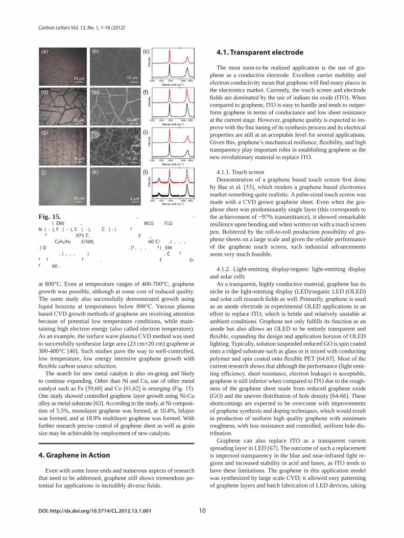
Yu et al. [57] took this further and produced uniform hexago-nal shaped graphene domains using the nucleation seeded growth method. Raman analysis revealed that the boundary lines of zig-zag edges of hexagonal graphene domains show smaller D-peak than do armchair edges, implying that the graphene with zigzag edges resulted in reduced defects and therefore exhibited better electronic qualities. Yu et al. [57] demonstrated a multiple elec-trode device made from two single crystal graphene domains shar-ing a boundary (Fig. 14). It was shown that because of the inter-domain boundary, the electron mobility is decreased and degrades the device performance. The group believes that improving the fabrication processes to make single crystalline, boundary-less, defect-subdued graphene sheet may be possible with further study.
Other than the aforementioned studies, persistent studies on top-ics such as the non-epitaxial nature of graphene growth, graphene-substrate interaction, graphene doping, and work-function control are being reported. All of these studies will shed more light on how to control graphene synthesis and properties and help develop gra-phene as a truly usable material for future electronics.
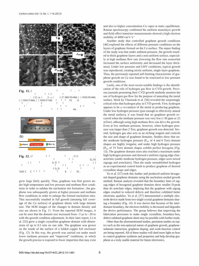
grew large fairly quickly. Thus, graphene was first grown un-der high temperature and low pressure and methane flow condi-tions in order to subdue the nucleation site formation ; the gra-phene was subsequently grown at higher pressure and methane flow conditions in order to enlarge the formed nucleation sites. This successfully resulted in full growth (meaning full cover-age of the Cu surface) of graphene sheets with large domain size. The SEM images of the changes in domain density and size are shown in Fig. 11. From the reported SEM images, it can be seen that the domain size increased from ~5 μr to ~20 to with the growth condition adjustment. In their later report, Li et al. [55] grew a single crystalline graphene domain with dimen-sions of up to 0.5 mm on one side. The graphene was grown on the inside of the surface of a folded copper foil enclosure (Fig. 12). In this way, the growth was carried out under much lower methane pressure and “improved” conditions, in which the growth process is exposed to fewer impurities that may exist
Fig. 11. Controlled growth of graphene domains. Scanning electron microscope images of partially grown graphene under dierent growth conditions: T (°C), JMe (sccm)/PMe (mTorr): (a) 985/35/460, (b) 1035/35/460, (c) 1035/7/460, (d) 1035/7/160. Scale bars are 10 μm. As seen from the images, lower density of seed domain is achieved with higher tempera-ture and lower methane ow settings and large single crystal growth is achieved by lowering the methane partial pressure [44].
Fig. 12. Large single crystal growth of graphene. (a) Copper foil enclo-sure prior to insertion in the furnace for chemical vapor deposition (CVD) growth. (b) Schematics of the CVD system for graphene on copper. (c) Scanning electron microscope image of a large single crystal graphene on enclosed copper foil grown by CVD. The graphene domain is grown at 1035°C on Cu at an average growth rate of ~6 μm/min [55].
Overview of graphene synthesis and applications
9 http://carbonlett.org
would be less energy intensive and therefore favorable for indus-trial production. Graphene growth with solid and liquid carbon source has also been shown in recent studies and the use of these sources allows for good quality monolayer graphene growth at lower temperatures [58]. For example, PMMA was used as a solid source and monolayer graphene was successfully grown
3.3.4. Recent CVD techniquesDemonstration of a 30’’ scale graphene sheet has directed
much focus to CVD growth on Cu using methane. But the on-going graphene synthesis research is not limited to this partic-ular process alone. One of the methods receiving attention is the growth of graphene at low temperatures, as such a process
Fig. 13. Eect of hydrogen on graphene grain (domain) shape. The average size of graphene grains grown for 30 min at 1000°C on Cu foil using 30 ppm methane in Ar mixture at 1 atm, as a function of partial pressure of hydrogen. The gures illustrate scanning electron microscope images of the typical shapes under these dierent conditions. Note that perfect hexagons are observed only at higher hydrogen pressures. Irregularly shaped grains grown at low hydrogen pressure. Scale bars are 10 μm (top two images) and 3 μm (bottom two images) [56].
Fig. 14. Electronic transport cross a single grain boundary. (a) Optical image of a device with multiple electrodes (numbered 1-10) contacting two co-alesced graphene grains (indicated by dashed lines). (b) Representative room-temperature I-V curves measured within each graphene grains and across the grain boundary. The measurements shown were performed at zero magnetic eld, and using four-probe congurations, with contacts ‘1’ and ‘6’ as cur-rent leads, and the 3 pairs of voltage leads labeled in the legend. (c) Four-terminal magnetoresistance (Rxx) measured at 4.3 K within each graphene grain
The most soon-to-be realized application is the use of gra-phene as a conductive electrode. Excellent carrier mobility and electron conductivity mean that graphene will find many places in the electronics market. Currently, the touch screen and electrode fields are dominated by the use of indium tin oxide (ITO). When compared to graphene, ITO is easy to handle and tends to outper-form graphene in terms of conductance and low sheet resistance at the current stage. However, graphene quality is expected to im-prove with the fine tuning of its synthesis process and its electrical properties are still at an acceptable level for several applications. Given this, graphene’s mechanical resilience, flexibility, and high transparency play important roles in establishing graphene as the new revolutionary material to replace ITO.
4.1.1. Touch screenDemonstration of a graphene based touch screen first done
by Bae et al. [53], which renders a graphene based electronics market something quite realistic. A palm-sized touch screen was made with a CVD grown graphene sheet. Even when the gra-phene sheet was predominantly single layer (this corresponds to the achievement of ~97% transmittance), it showed remarkable resilience upon bending and when written on with a touch screen pen. Bolstered by the roll-to-roll production possibility of gra-phene sheets on a large scale and given the reliable performance of the graphene touch screen, such industrial advancements seem very much feasible.
4.1.2. Light-emitting display/organic light-emitting display and solar cells
As a transparent, highly conductive material, graphene has its niche in the light-emitting display (LED)/organic LED (OLED) and solar cell research fields as well. Primarily, graphene is used as an anode electrode in experimental OLED applications in an effort to replace ITO, which is brittle and relatively unstable at ambient conditions. Graphene not only fulfills its function as an anode but also allows an OLED to be entirely transparent and flexible, expanding the design and application horizon of OLED lighting. Typically, solution suspended reduced GO is spin coated onto a ridged substrate such as glass or is mixed with conducting polymer and spin coated onto flexible PET [64,65]. Most of the current research shows that although the performance (light emit-ting efficiency, sheet resistance, electron leakage) is acceptable, graphene is still inferior when compared to ITO due to the rough-ness of the graphene sheet made from reduced graphene oxide (GO) and the uneven distribution of hole density [64-66]. These shortcomings are expected to be overcome with improvements of graphene synthesis and doping techniques, which would result in production of uniform high quality graphene with minimum roughness, with less resistance and controlled, uniform hole dis-tribution.
Graphene can also replace ITO as a transparent current spreading layer in LED [67]. The outcome of such a replacement is improved transparency in the blue and near-infrared light re-gions and increased stability in acid and bases, as ITO tends to have these limitations. The graphene in this application model was synthesized by large scale CVD; it allowed easy patterning of graphene layers and batch fabrication of LED devices, taking
at 800°C. Even at temperature ranges of 400-700°C, graphene growth was possible, although at some cost of reduced quality. The same study also successfully demonstrated growth using liquid benzene at temperatures below 800°C. Various plasma based CVD growth methods of graphene are receiving attention because of potential low temperature conditions, while main-taining high electron energy (also called electron temperature). As an example, the surface wave plasma CVD method was used to successfully synthesize large area (23 cm×20 cm) graphene at 300-400°C [40]. Such studies pave the way to well-controlled, low temperature, low energy intensive graphene growth with flexible carbon source selection.
The search for new metal catalyst is also on-going and likely to continue expanding. Other than Ni and Cu, use of other metal catalyst such as Fe [59,60] and Co [61,62] is emerging (Fig. 15). One study showed controlled graphene layer growth using Ni-Cu alloy as metal substrate [63]. According to the study, at Ni composi-tion of 5.5%, monolayer graphene was formed, at 10.4%, bilayer was formed, and at 18.9% multilayer graphene was formed. With further research precise control of graphene sheet as well as grain size may be achievable by employment of new catalysts.
4. Graphene in Action
Even with some loose ends and numerous aspects of research that need to be addressed, graphene still shows tremendous po-tential for applications in incredibly diverse fields.
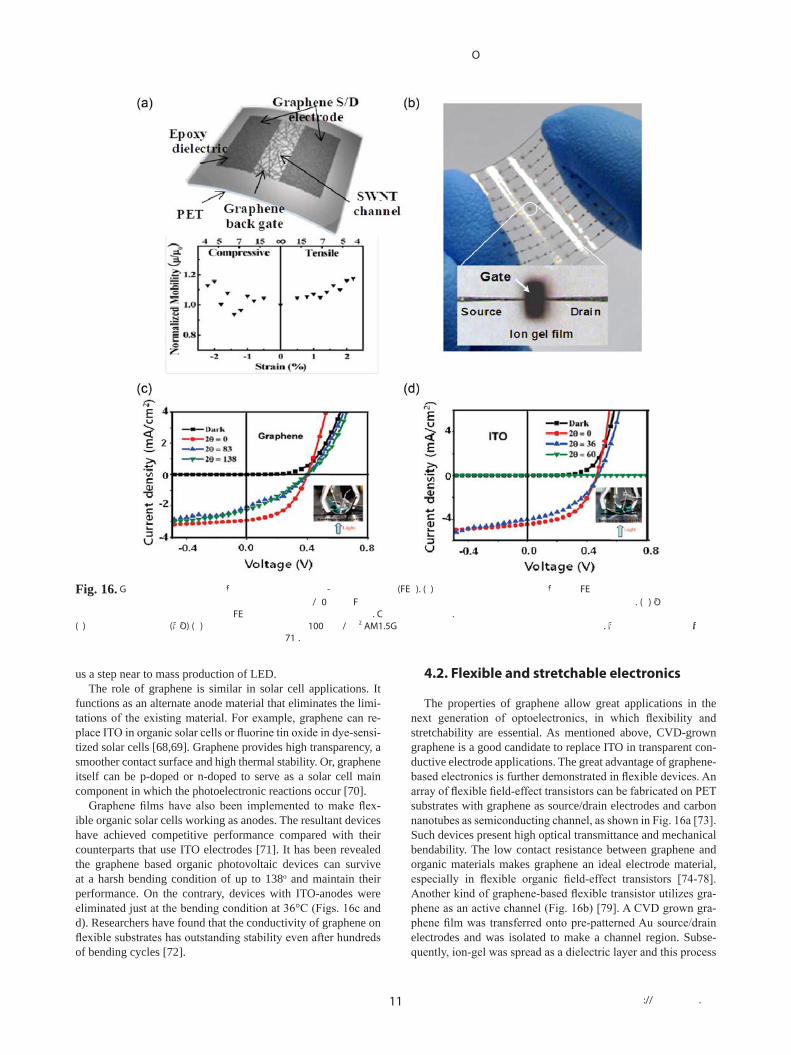
Fig. 15. Typical optical microscopy images, scanning electron micro-scope (SEM) images, and Raman spectroscopy of MLG and FLG grown on Ni (a-c), Fe (d-f ), Co (g-i), and Cu (j-l) foil substrates using ethylene as the carbon source at 975°C. The growth time was 3 min, and the gas mixing ratio of C2H4/H2 was 5/500, and the cooling rate was 60°C/min. (a, d, g, and j) Optical microscope images of graphene. (b, e, h, and k) SEM images of graphene. (c, f, i, and l) Raman spectroscopy of graphene. Cu substrate background was subtracted. The spectra were normalized with the G-band [60].
Overview of graphene synthesis and applications
11 http://carbonlett.org
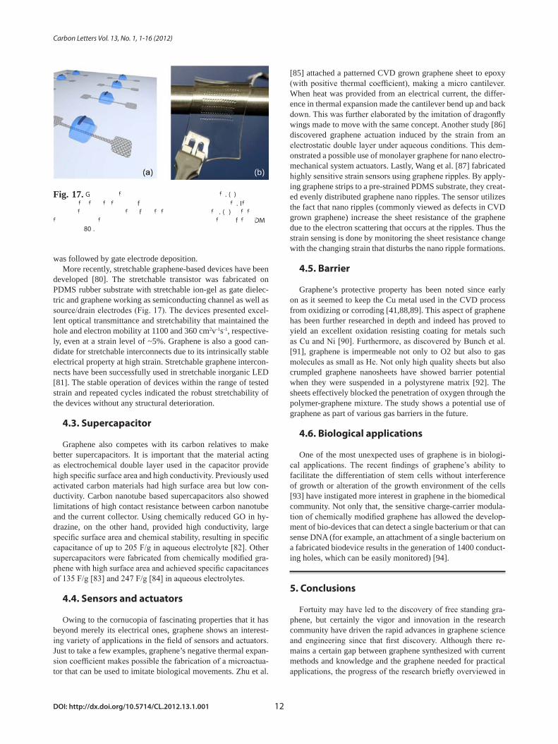
4.2. Flexible and stretchable electronics
The properties of graphene allow great applications in the next generation of optoelectronics, in which flexibility and stretchability are essential. As mentioned above, CVD-grown graphene is a good candidate to replace ITO in transparent con-ductive electrode applications. The great advantage of graphene-based electronics is further demonstrated in flexible devices. An array of flexible field-effect transistors can be fabricated on PET substrates with graphene as source/drain electrodes and carbon nanotubes as semiconducting channel, as shown in Fig. 16a [73]. Such devices present high optical transmittance and mechanical bendability. The low contact resistance between graphene and organic materials makes graphene an ideal electrode material, especially in flexible organic field-effect transistors [74-78]. Another kind of graphene-based flexible transistor utilizes gra-phene as an active channel (Fig. 16b) [79]. A CVD grown gra-phene film was transferred onto pre-patterned Au source/drain electrodes and was isolated to make a channel region. Subse-quently, ion-gel was spread as a dielectric layer and this process
us a step near to mass production of LED. The role of graphene is similar in solar cell applications. It
functions as an alternate anode material that eliminates the limi-tations of the existing material. For example, graphene can re-place ITO in organic solar cells or fluorine tin oxide in dye-sensi-tized solar cells [68,69]. Graphene provides high transparency, a smoother contact surface and high thermal stability. Or, graphene itself can be p-doped or n-doped to serve as a solar cell main component in which the photoelectronic reactions occur [70].
Graphene films have also been implemented to make flex-ible organic solar cells working as anodes. The resultant devices have achieved competitive performance compared with their counterparts that use ITO electrodes [71]. It has been revealed the graphene based organic photovoltaic devices can survive at a harsh bending condition of up to 138o and maintain their performance. On the contrary, devices with ITO-anodes were eliminated just at the bending condition at 36°C (Figs. 16c and d). Researchers have found that the conductivity of graphene on flexible substrates has outstanding stability even after hundreds of bending cycles [72].
Fig. 16. Graphene application for exible transparent eld-eect transistor (FET). (a) Schematic structure of the exible FETs on the plastic substrate and the change in the normalized eective device mobility μ/μ0 for TTFTs as a function of the bending induced strain and bending radius. (b) Optical images of an array of ion gel gated graphene FET devices on a plastic substrate. Current density vs. voltage characteristics of chemical vapor deposition graphene (c) or indium tin oxide (ITO) (d) photovoltaic cells under 100 mW/cm2 AM1.5G spectral illumination for dierent bending angles. Insets in c and d show the experimental setup employed in the experiments [71].
[85] attached a patterned CVD grown graphene sheet to epoxy (with positive thermal coefficient), making a micro cantilever. When heat was provided from an electrical current, the differ-ence in thermal expansion made the cantilever bend up and back down. This was further elaborated by the imitation of dragonfly wings made to move with the same concept. Another study [86] discovered graphene actuation induced by the strain from an electrostatic double layer under aqueous conditions. This dem-onstrated a possible use of monolayer graphene for nano electro-mechanical system actuators. Lastly, Wang et al. [87] fabricated highly sensitive strain sensors using graphene ripples. By apply-ing graphene strips to a pre-strained PDMS substrate, they creat-ed evenly distributed graphene nano ripples. The sensor utilizes the fact that nano ripples (commonly viewed as defects in CVD grown graphene) increase the sheet resistance of the graphene due to the electron scattering that occurs at the ripples. Thus the strain sensing is done by monitoring the sheet resistance change with the changing strain that disturbs the nano ripple formations.
4.5. Barrier
Graphene’s protective property has been noted since early on as it seemed to keep the Cu metal used in the CVD process from oxidizing or corroding [41,88,89]. This aspect of graphene has been further researched in depth and indeed has proved to yield an excellent oxidation resisting coating for metals such as Cu and Ni [90]. Furthermore, as discovered by Bunch et al. [91], graphene is impermeable not only to O2 but also to gas molecules as small as He. Not only high quality sheets but also crumpled graphene nanosheets have showed barrier potential when they were suspended in a polystyrene matrix [92]. The sheets effectively blocked the penetration of oxygen through the polymer-graphene mixture. The study shows a potential use of graphene as part of various gas barriers in the future.
4.6. Biological applications
One of the most unexpected uses of graphene is in biologi-cal applications. The recent findings of graphene’s ability to facilitate the differentiation of stem cells without interference of growth or alteration of the growth environment of the cells [93] have instigated more interest in graphene in the biomedical community. Not only that, the sensitive charge-carrier modula-tion of chemically modified graphene has allowed the develop-ment of bio-devices that can detect a single bacterium or that can sense DNA (for example, an attachment of a single bacterium on a fabricated biodevice results in the generation of 1400 conduct-ing holes, which can be easily monitored) [94].
5. Conclusions
Fortuity may have led to the discovery of free standing gra-phene, but certainly the vigor and innovation in the research community have driven the rapid advances in graphene science and engineering since that first discovery. Although there re-mains a certain gap between graphene synthesized with current methods and knowledge and the graphene needed for practical applications, the progress of the research briefly overviewed in
was followed by gate electrode deposition. More recently, stretchable graphene-based devices have been
developed [80]. The stretchable transistor was fabricated on PDMS rubber substrate with stretchable ion-gel as gate dielec-tric and graphene working as semiconducting channel as well as source/drain electrodes (Fig. 17). The devices presented excel-lent optical transmittance and stretchability that maintained the hole and electron mobility at 1100 and 360 cm2v-1s-1, respective-ly, even at a strain level of ~5%. Graphene is also a good can-didate for stretchable interconnects due to its intrinsically stable electrical property at high strain. Stretchable graphene intercon-nects have been successfully used in stretchable inorganic LED [81]. The stable operation of devices within the range of tested strain and repeated cycles indicated the robust stretchability of the devices without any structural deterioration.
4.3. Supercapacitor
Graphene also competes with its carbon relatives to make better supercapacitors. It is important that the material acting as electrochemical double layer used in the capacitor provide high specific surface area and high conductivity. Previously used activated carbon materials had high surface area but low con-ductivity. Carbon nanotube based supercapacitors also showed limitations of high contact resistance between carbon nanotube and the current collector. Using chemically reduced GO in hy-drazine, on the other hand, provided high conductivity, large specific surface area and chemical stability, resulting in specific capacitance of up to 205 F/g in aqueous electrolyte [82]. Other supercapacitors were fabricated from chemically modified gra-phene with high surface area and achieved specific capacitances of 135 F/g [83] and 247 F/g [84] in aqueous electrolytes.
4.4. Sensors and actuators
Owing to the cornucopia of fascinating properties that it has beyond merely its electrical ones, graphene shows an interest-ing variety of applications in the field of sensors and actuators. Just to take a few examples, graphene’s negative thermal expan-sion coefficient makes possible the fabrication of a microactua-tor that can be used to imitate biological movements. Zhu et al.
Fig. 17. Graphene for stretchable transparent transistor. (a) Schematic illustration of monolithically patterned graphene transistor. Ion gel is printed on channel region by aerosol printing method. (b) Photograph of stretchable ion gel gate dielectric graphene transistor array on PDMS substrate [80].
Overview of graphene synthesis and applications
13 http://carbonlett.org
org/10.1038/nnano.2009.58.[14] Dikin DA, Stankovich S, Zimney EJ, Piner RD, Dommett GHB,
Evmenenko G, Nguyen ST, Ruoff RS. Preparation and character-ization of graphene oxide paper. Nature, 448, 457 (2007). http://dx.doi.org/10.1038/nature06016.
[15] Park S, Lee KS, Bozoklu G, Cai W, Nguyen SBT, Ruoff RS. Gra-phene oxide papers modified by divalent ions--enhancing me-chanical properties via chemical cross-linking. ACS Nano, 2, 572 (2008). http://dx.doi.org/10.1021/nn700349a.
[16] Kumar A, Reddy ALM, Mukherjee A, Dubey M, Zhan X, Singh N, Ci L, Billups WE, Nagurny J, Mital G, Ajayan PM. Direct synthesis of lithium-intercalated graphene for electrochemical en-ergy storage application. ACS Nano, 5, 4345 (2011). http://dx.doi.org/10.1021/nn201527p.
[17] Zhu Y, Murali S, Stoller MD, Velamakanni A, Piner RD, Ruoff RS. Microwave assisted exfoliation and reduction of graphite oxide for ultracapacitors. Carbon, 48, 2118 (2010). http://dx.doi.org/10.1016/j.carbon.2010.02.001.
[18] Murugan AV, Muraliganth T, Manthiram A. Rapid, facile micro-wave-solvothermal synthesis of graphene nanosheets and their polyaniline nanocomposites for energy strorage. Chem Mater, 21, 5004 (2009). http://dx.doi.org/10.1021/cm902413c.
[19] Long J, Fang M, Chen G. Microwave-assisted rapid synthesis of water-soluble graphene. J Mater Chem, 21, 10421 (2011). http://dx.doi.org/10.1039/c0jm04564k.
[20] Charrier A, Coati A, Argunova T, Thibaudau F, Garreau Y, Pinch-aux R, Forbeaux I, Debever JM, Sauvage-Simkin M, Themlin JM. Solid-state decomposition of silicon carbide for growing ultra-thin heteroepitaxial graphite films. J Appl Phys, 92, 2479 (2002). http://dx.doi.org/10.1063/1.1498962.
[21] Forbeaux I, Themlin JM, Debever JM. Heteroepitaxial graphite on 6H-SiC(0001): Interface formation through conduction-band electronic structure. Phys Rev B, 58, 16396 (1998). http://dx.doi.org/10.1103/PhysRevB.58.16396.
[22] Tung RT, Gibson JM, Poate JM. Formation of ultrathin dingle-crystal silicide films on Si: surface and interfacial stabilization of Si-NiSi2 epitaxial structures. Phys Rev Lett, 50, 429 (1983). http://dx.doi.org/10.1103/PhysRevLett.50.429.
[23] Edman L, Sundqvist B, McRae E, Litvin-Staszewska E. Electrical resistivity of single-crystal graphite under pressure: an anisotropic three-dimensional semimetal. Phys Rev B, 57, 6227 (1998). http://dx.doi.org/10.1103/PhysRevB.57.6227.
[24] Binns C, Baker SH, Demangeat C, Parlebas JC. Growth, electron-ic, magnetic and spectroscopic properties of transition metals on graphite. Surf Sci Rep, 34, 107 (1999). http://dx.doi.org/10.1016/S0167-5729(99)00004-7.
[25] Kopelevich Y, Esquinazi P, Torres JHS, Moehlecke S. Ferromagnet-ic- and superconducting-like behavior of graphite. J Low Temp Phys, 119, 691 (2000). http://dx.doi.org/10.1023/A:1004637814008.
[26] Berger C, Song Z, Li T, Li X, Ogbazghi AY, Feng R, Dai Z, Alexei N, Conrad MEH, First PN, De Heer WA. Ultrathin epitaxial graph-ite: 2D electron gas properties and a route toward graphene-based nanoelectronics. J Phys Chem B, 108, 19912 (2004). http://dx.doi.org/10.1021/jp040650f.
[27] Lee DS, Riedl C, Krauss B, Klitzing KV, Starke U, Smet JH. Ra-man spectra of epitaxial graphene on SiC and of epitaxial graphene transferred to SiO2. Nano Lett, 8, 4320 (2008). http://dx.doi.org/10.1021/nl802156w.
[28] Unarunotai S, Murata Y, Chialvo CE, Kim HS, MacLaren S, Ma-
this paper assures continued improvements. Full implementa-tion of graphene based electronics and consumer products may come about with the fine-tuning of the growth process, which will reduce damages that occur during etching and transfer and allow the acquisition of definite control over graphene’s electri-cal properties.
Acknowledgements
This work was supported by the National Research Foun-dation of Korea (NRF) funded by the Ministry of Education, Science and Technology (Global Research Lab. 2011-001758, 2011K00061, 20110017587, 20110006268, Global Frontier Re-search Program 20110031629).
References
[1] Peierls RE. Quelques proprieties typiques des corpses solides. Ann I H Poincare, 5, 177 (1935).
[2] Landau LD. Zur Theorie der phasenumwandlungen II. Phys Z Sowjetunion, 11, 26 (1937).
[3] Geim AK, Novoselov KS. The rise of graphene. Nature Mater, 6, 183 (2007). http://dx.doi.org/10.1038/nmat1849.
[4] Novoselov KS, Geim AK, Morozov SV, Jiang D, Zhang Y, Dubo-nos SV, Grigorieva IV, Firsov AA. Electric field in atomically thin carbon films. Science, 306, 666 (2004). http://dx.doi.org/10.1126/science.1102896.
[5] Novoselov KS, Jiang D, Schedin F, Booth TJ, Khotkevich VV, Mo-rozov SV, Geim AK. Two-dimensional atomic crystals. Proc Natl Acad Sci U S A, 102, 10451 (2005). http://dx.doi.org/10.1073/pnas.0502848102.
[6] Bolotin KI, Sikes KJ, Jiang Z, Klima M, Fudenberg G, Hone J, Kim P, Stormer HL. Ultrahigh electron mobility in suspended graphene. Solid State Commun, 146, 351 (2008). http://dx.doi.org/10.1016/j.ssc.2008.02.024.
[7] Morozov SV, Novoselov KS, Katsnelson MI, Schedin F, Elias DC, Jaszczak JA, Geim AK. Giant intrinsic carrier mobilities in gra-phene and its bilayer. Phys Rev Lett, 100, 016602 (2008). http://dx.doi.org/10.1103/PhysRevLett.100.016602.
[8] Balandin AA, Ghosh S, Bao W, Calizo I, Teweldebrhan D, Miao F, Lau CN. Superior thermal conductivity of single-layer graphene. Nano Lett, 8, 902 (2008). http://dx.doi.org/10.1021/nl0731872.
[9] Lee C, Wei X, Kysar JW, Hone J. Measurement of the elastic prop-erties and intrinsic strength of monolayer graphene. Science, 321, 385 (2008). http://dx.doi.org/10.1126/science.1157996.
[10] Zhu Y, Murali S, Cai W, Li X, Suk JW, Potts JR, Ruoff RS. Gra-phene and graphene oxide: synthesis, properties, and applica-tions. Adv Mater, 22, 3906 (2010). http://dx.doi.org/10.1002/adma.201001068.
[11] Zhang Y, Small JP, Pontius WV, Kim P. Fabrication and electric-field-dependent transport measurements of mesoscopic graph-ite devices. Appl Phys Lett, 86, 073104 (2005). http://dx.doi.org/10.1063/1.1862334.
[12] Geim AK. Graphene: status and prospects. Science, 324, 1530 (2009). http://dx.doi.org/10.1126/science.1158877.
[13] Park S, Ruoff RS. Chemical methods for the production of graphenes. Nature Nanotechnol, 4, 217 (2009). http://dx.doi.
[43] Li X, Cai W, Colombo L, Ruoff RS. Evolution of graphene growth on Ni and Cu by carbon isotope labeling. Nano Lett, 9, 4268 (2009). http://dx.doi.org/10.1021/nl902515k.
[44] Li X, Magnuson CW, Venugopal A, An J, Suk JW, Han B, Borysiak M, Cai W, Velamakanni A, Zhu Y, Fu L, Vogel EM, Voelkl E, Co-lombo L, Ruoff RS. Graphene films with large domain size by a two-step chemical vapor deposition process. Nano Lett, 10, 4328 (2010). http://dx.doi.org/10.1021/nl101629g.
[45] Li X, Cai W, An J, Kim S, Nah J, Yang D, Piner R, Velamakanni A, Jung I, Tutuc E, Banerjee SK, Colombo L, Ruoff RS. Large-area synthesis of high-quality and uniform graphene films on copper foils. Science, 324, 1312 (2009). http://dx.doi.org/10.1126/sci-ence.1171245.
[46] Bhaviripudi S, Jia X, Dresselhaus MS, Kong J. Role of kinetic fac-tors in chemical vapor deposition synthesis of uniform large area graphene using copper catalyst. Nano Lett, 10, 4128 (2010). http://dx.doi.org/10.1021/nl102355e.
[47] Li X, Zhu Y, Cai W, Borysiak M, Han B, Chen D, Piner RD, Co-lomba L, Ruoff RS. Transfer of large-area graphene films for high-performance transparent conductive electrodes. Nano Lett, 9, 4359 (2009). http://dx.doi.org/10.1021/nl902623y.
[48] Ferrari AC, Meyer JC, Scardaci V, Casiraghi C, Lazzeri M, Mauri F, Piscanec S, Jiang D, Novoselov KS, Roth S, Geim AK. Raman spectrum of graphene and graphene layers. Phys Rev Lett, 97, 187401 (2006). http://dx.doi.org/10.1103/PhysRevLett.97.187401.
[49] Cancado LG, Jorio A, Ferreira EHM, Stavale F, Achete CA, Ca-paz RB, Moutinho MVO, Lombardo A, Kulmala TS, Ferrari AC. Quantifying defects in graphene via Raman spectroscopy at differ-ent excitation energies. Nano Lett, 11, 3190 (2011). http://dx.doi.org/10.1021/nl201432g.
[50] Dresselhaus MS, Jorio A, Hofmann M, Dresselhaus G, Saito R. Perspectives on carbon nanotubes and graphene Raman spec-troscopy. Nano Lett, 10, 751 (2010). http://dx.doi.org/10.1021/nl904286r.
[51] Molitor F, Graf D, Stampfer C, Ihn T, Ensslin K. Raman imaging and electronic properties of graphene. Adv Solid State Phys, 47, 171 (2008). http://dx.doi.org/10.1007/978-3-540-74325-5_14.
[52] Lee Y, Bae S, Jang H, Jang S, Zhu SE, Sim SH, Song YI, Hong BH, Ahn JH. Wafer-scale synthesis and transfer of graphene films. Nano Lett, 10, 490 (2010). http://dx.doi.org/10.1021/nl903272n.
[53] Bae S, Kim H, Lee Y, Xu X, Park JS, Zheng Y, Balakrishnan J, Lei T, Ri Kim H, Song YI, Kim YJ, Kim KS, Ozyilmaz B, Ahn JH, Hong BH, Iijima S. Roll-to-roll production of 30-inch gra-phene films for transparent electrodes. Nature Nanotechnol, 5, 574 (2010). http://dx.doi.org/10.1038/nnano.2010.132.
[54] Zhang W, Wu P, Li Z, Yang J. First-principles thermodynamics of graphene growth on Cu surfaces. J Phys Chem C, 115, 17782 (2011). http://dx.doi.org/10.1021/jp2006827.
[55] Li X, Magnuson CW, Venugopal A, Tromp RM, Hannon JB, Vo-gel EM, Colombo L, Ruoff RS. Large-area graphene single crys-tals grown by low-pressure chemical vapor deposition of meth-ane on copper. J Am Chem Soc, 133, 2816 (2011). http://dx.doi.org/10.1021/ja109793s.
[56] Vlassiouk I, Regmi M, Fulvio P, Dai S, Datskos P, Eres G, Smirnov S. Role of hydrogen in chemical vapor deposition growth of large single-crystal graphene. ACS Nano, 5, 6069 (2011). http://dx.doi.org/10.1021/nn201978y.
son N, Petrov I, Rogers JA. Transfer of graphene layers grown on SiC wafers to other substrates and their integration into field ef-fect transistors. Appl Phys Lett, 95, 202101 (2009). http://dx.doi.org/10.1063/1.3263942.
[29] Caldwell JD, Anderson TJ, Culbertson JC, Jernigan GG, Hobart KD, Kub FJ, Tadjer MJ, Tedesco JL, Hite JK, Mastro MA, Myers-Ward RL, Eddy Jr CR, Campbell PM, Gaskill DK. Technique for the dry transfer of epitaxial graphene onto arbitrary substrates. ACS Nano, 4, 1108 (2010). http://dx.doi.org/10.1021/nn901585p.
[30] Unarunotai S, Koepke JC, Tsai CL, Du F, Chialvo CE, Murata Y, Haasch R, Petrov I, Mason N, Shim M, Lyding J, Rogers JA. Layer-by-layer transfer of multiple, large area sheets of graphene grown in multilayer stacks on a single SiC wafer. ACS Nano, 4, 5591 (2010). http://dx.doi.org/10.1021/nn101896a.
[31] Vaari J, Lahtinen J, Hautojarvi P. The adsorption and decomposi-tion of acetylene on clean and K-covered Co(0001). Catal Lett, 44, 43 (1997). http://dx.doi.org/10.1023/A:1018972924563.
[32] Ueta H, Saida M, Nakai C, Yamada Y, Sasaki M, Yamamoto S. Highly oriented monolayer graphite formation on Pt(1 1 1) by a supersonic methane beam. Surf Sci, 560, 183 (2004). http://dx.doi.org/10.1016/j.susc.2004.04.039.
[33] Starr DE, Pazhetnov EM, Stadnichenko AI, Boronin AI, Shai-khutdinov SK. Carbon films grown on Pt(1 1 1) as supports for model gold catalysts. Surf Sci, 600, 2688 (2006). http://dx.doi.org/10.1016/j.susc.2006.04.035.
[34] Gall NR, Rut’kov EV, Tontegode AY. Interaction of silver atoms with iridium and with a two-dimensional graphite film on iridium: adsorption, desorption, and dissolution. Phys Solid State, 46, 371 (2004). http://dx.doi.org/10.1134/1.1649439.
[35] Coraux J, N’Diaye AT, Busse C, Michely T. Structural coherency of graphene on Ir(111). Nano Lett, 8, 565 (2008). http://dx.doi.org/10.1021/nl0728874.
[36] Vazquez De Parga AL, Calleja F, Borca B, Passeggi MCG, Hi-narejos JJ, Guinea F, Miranda R. Periodically rippled graphene: growth and spatially resolved electronic structure. Phys Rev Lett, 100, 056807 (2008). http://dx.doi.org/10.1103/PhysRevLett. 100.056807.
[37] Marchini S, Gunther S, Wintterlin J. Scanning tunneling micros-copy of graphene on Ru(0001). Phys Rev B, 76, 075429 (2007). http://dx.doi.org/10.1103/PhysRevB.76.075429.
[38] Reina A, Jia X, Ho J, Nezich D, Son H, Bulovic V, Dresselhaus MS, Jing K. Large area, few-layer graphene films on arbitrary substrates by chemical vapor deposition. Nano Lett, 9, 30 (2009). http://dx.doi.org/10.1021/nl801827v.
[39] Yu Q, Lian J, Siriponglert S, Li H, Chen YP, Pei SS. Graphene segregated on Ni surfaces and transferred to insulators. Appl Phys Lett, 93, 113103 (2008). http://dx.doi.org/10.1063/1.2982585.
[40] Kim J, Ishihara M, Koga Y, Tsugawa K, Hasegawa M, Iijima S. Low-temperature synthesis of large-area graphene-based trans-parent conductive films using surface wave plasma chemical va-por deposition. Appl Phys Lett, 98, 091502 (2011). http://dx.doi.org/10.1063/1.3561747.
[41] Reina A, Thiele S, Jia X, Bhaviripudi S, Dresselhaus M, Schae-fer J, Kong J. Growth of large-area single- and Bi-layer graphene by controlled carbon precipitation on polycrystalline Ni surfaces. Nano Res, 2, 509 (2009). http://dx.doi.org/10.1007/s12274-009-9059-y.
[42] Kim KS, Zhao Y, Jang H, Lee SY, Kim JM, Ahn JH, Kim P, Choi JY, Hong BH. Large-scale pattern growth of graphene films for
Overview of graphene synthesis and applications
15 http://carbonlett.org
Nano, 4, 2865 (2010). http://dx.doi.org/10.1021/nn901587x.[72] Li SS, Tu KH, Lin CC, Chen CW, Chhowalla M. Solution-process-
able graphene oxide as an efficient hole transport layer in polymer solar cells. ACS Nano, 4, 3169 (2010). http://dx.doi.org/10.1021/nn100551j.
[73] Jang S, Jang H, Lee Y, Suh D, Baik S, Hee Hong B, Ahn JH. Flex-ible, transparent single-walled carbon nanotube transistors with grapheme electrodes. Nanotechnology, 21, 425201 (2010). http://dx.doi.org/10.1088/0957-4484/21/42/425201.
[74] Lee WH, Park J, Sim SH, Jo SB, Kim KS, Hong BH, Cho K. Trans-parent flexible organic transistors based on monolayer graphene electrodes on plastic. Adv Mater, 23, 1752 (2011). http://dx.doi.org/10.1002/adma.201004099.
[75] Gundlach DJ, Zhou L, Nichols JA, Jackson TN, Necliudov PV, Shur MS. An experimental study of contact effects in organic thin film transistors. J Appl Phys, 100, 024509 (2006). http://dx.doi.org/10.1063/1.2215132.
[76] Necliudov PV, Shur MS, Gundlach DJ, Jackson TN. Contact resistance extraction in pentacene thin film transistors. Solid-State Electron, 47, 259 (2003). http://dx.doi.org/10.1016/s0038-1101(02)00204-6.
[77] Blanchet GB, Fincher CR, Lefenfeld M, Rogers JA. Contact re-sistance in organic thin film transistors. Appl Phys Lett, 84, 296 (2004). http://dx.doi.org/10.1063/1.1639937.
[78] Becerril HA, Stoltenberg RM, Tang ML, Roberts ME, Liu Z, Chen Y, Kim DH, Lee BL, Lee S, Bao Z. Fabrication and evaluation of solution-processed reduced graphene oxide electrodes for p- and n-channel bottom-contact organic thin-film transistors. ACS Nano, 4, 6343 (2010). http://dx.doi.org/10.1021/nn101369j.
[79] Kim BJ, Jang H, Lee SK, Hong BH, Ahn JH, Cho JH. High-per-formance flexible graphene field effect transistors with ion gel gate dielectrics. Nano Lett, 10, 3464 (2010). http://dx.doi.org/10.1021/nl101559n.
[80] Lee SK, Kim BJ, Jang H, Yoon SC, Lee C, Hong BH, Rogers JA, Cho JH, Ahn JH. Stretchable graphene transistors with printed di-electrics and gate electrodes. Nano Lett, 11, 4642 (2011). http://dx.doi.org/10.1021/nl202134z.
[81] Kim RH, Bae MH, Kim DG, Cheng H, Kim BH, Kim DH, Li M, Wu J, Du F, Kim HS, Kim S, Estrada D, Hong SW, Huang Y, Pop E, Rogers JA. Stretchable, transparent graphene interconnects for arrays of microscale inorganic light emitting diodes on rubber substrates. Nano Lett, 11, 3881 (2011). http://dx.doi.org/10.1021/nl202000u.
[82] Wang Y, Shi Z, Huang Y, Ma Y, Wang C, Chen M, Chen Y. Super-capacitor devices based on graphene materials. J Phys Chem C, 113, 13103 (2009). http://dx.doi.org/10.1021/jp902214f.
[83] Stoller MD, Park S, Yanwu Z, An J, Ruoff RS. Graphene-based ul-tracapacitors. Nano Lett, 8, 3498 (2008). http://dx.doi.org/10.1021/nl802558y.
[85] Zhu SE, Shabani R, Rho J, Kim Y, Hong BH, Ahn JH, Cho HJ. Graphene-based bimorph microactuators. Nano Lett, 11, 977 (2011). http://dx.doi.org/10.1021/nl103618e.
[86] Rogers GW, Liu JZ. Graphene actuators: quantum-mechanical and electrostatic double-layer effects. J Am Chem Soc, 133, 10858 (2011). http://dx.doi.org/10.1021/ja201887r.
[57] Yu Q, Jauregui LA, Wu W, Colby R, Tian J, Su Z, Cao H, Liu Z, Pandey D, Wei D, Chung TF, Peng P, Guisinger NP, Stach EA, Bao J, Pei SS, Chen YP. Control and characterization of individ-ual grains and grain boundaries in graphene grown by chemical vapour deposition. Nature Mater, 10, 443 (2011). http://dx.doi.org/10.1038/nmat3010.
[58] Sun Z, Yan Z, Yao J, Beitler E, Zhu Y, Tour JM. Growth of gra-phene from solid carbon sources. Nature, 468, 549 (2010). http://dx.doi.org/10.1038/nature09579.
[59] Kondo D, Sato S, Yagi K, Harada N, Sato M, Nihei M, Yokoya-ma N. Low-temperature synthesis of graphene and fabrication of top-gated field effect transistors without using transfer processes. Appl Phys Express, 3, 025102 (2010). http://dx.doi.org/10.1143/apex.3.025102.
[60] Yao Y, Li Z, Lin Z, Moon KS, Agar J, Wong C. Controlled growth of multilayer, few-layer, and single-layer graphene on metal substrates. J Phys Chem C, 115, 5232 (2011). http://dx.doi.org/10.1021/jp109002p.
[61] Ago H, Ito Y, Mizuta N, Yoshida K, Hu B, Orofeo CM, Tsuji M, Ikeda KI, Mizuno S. Epitaxial chemical vapor deposition growth of single-layer graphene over cobalt film crystallized on sapphire. ACS Nano, 4, 7407 (2010). http://dx.doi.org/10.1021/nn102519b.
[62] Sukhdeo D. Large-area chemical vapor deposition of graphene over thin films of cobalt. The 2009 NNIN REU Research Accomplish-ments, National Nanotechnology Infrastructure Network, 100 (2009).
[63] Liu X, Fu L, Liu N, Gao T, Zhang Y, Liao L, Liu Z. Segregation growth of graphene on Cu-Ni alloy for precise layer control. J Phys Chem C, 115, 11976 (2011). http://dx.doi.org/10.1021/jp202933u.
[64] Wu J, Agrawal M, Becerril HA, Bao Z, Liu Z, Chen Y, Peumans P. Organic light-emitting diodes on solution-processed graphene transparent electrodes. ACS Nano, 4, 43 (2010). http://dx.doi.org/10.1021/nn900728d.
[65] Chang H, Wang G, Yang A, Tao X, Liu X, Shen Y, Zheng Z. A transparent, flexible, low-temperature, and solution-processible graphene composite electrode. Adv Funct Mater, 20, 2893 (2010). http://dx.doi.org/10.1002/adfm.201000900.
[66] Sun T, Wang ZL, Shi ZJ, Ran GZ, Xu WJ, Wang ZY, Li YZ, Dai L, Qin GG. Multilayered graphene used as anode of organic light emitting devices. Appl Phys Lett, 96, 133301 (2010). http://dx.doi.org/10.1063/1.3373855.
[67] Jo G, Choe M, Cho CY, Kim JH, Park W, Lee S, Hong WK, Kim TW, Park SJ, Hong BH, Kahng YH, Lee T. Large-scale patterned multi-layer graphene films as transparent conducting electrodes for GaN light-emitting diodes. Nanotechnology, 21, 175201 (2010). http://dx.doi.org/10.1088/0957-4484/21/17/175201.
[68] Wang Y, Tong SW, Xu XF, Ozyilmaz B, Loh KP. Interface engi-neering of layer-by-layer stacked graphene anodes for high-per-formance organic solar cells. Adv Mater, 23, 1514 (2011). http://dx.doi.org/10.1002/adma.201003673.
[69] Wang X, Zhi L, Mullen K. Transparent, conductive graphene elec-trodes for dye-sensitized solar cells. Nano Lett, 8, 323 (2008). http://dx.doi.org/10.1021/nl072838r.
[70] Ihm K, Lim JT, Lee KJ, Kwon JW, Kang TH, Chung S, Bae S, Kim JH, Hong BH, Yeom GY. Number of graphene layers as a modulator of the open-circuit voltage of graphene-based solar cell. Appl Phys Lett, 97, 0321133 (2010). http://dx.doi.org/10.1063/1.3464319.
[71] Gomez De Arco L, Zhang Y, Schlenker CW, Ryu K, Thompson ME, Zhou C. Continuous, highly flexible, and transparent graphene films by chemical vapor deposition for organic photovoltaics. ACS
JM, Craighead HG, McEuen PL. Impermeable atomic membranes from graphene sheets. Nano Lett, 8, 2458 (2008). http://dx.doi.org/10.1021/nl801457b.
[92] Compton OC, Kim S, Pierre C, Torkelson JM, Nguyen ST. Crum-pled graphene nanosheets as highly effective barrier property en-hancers. Adv Mater, 22, 4759 (2010). http://dx.doi.org/10.1002/adma.201000960.
[93] Nayak TR, Andersen H, Makam VS, Khaw C, Bae S, Xu X, Ee PLR, Ahn JH, Hong BH, Pastorin G, Özyilmaz B. Graphene for controlled and accelerated osteogenic differentiation of human mesenchymal stem cells. ACS Nano, 5, 4670 (2011). http://dx.doi.org/10.1021/nn200500h.
[94] Mohanty N, Berry V. Graphene-based single-bacterium resolution biodevice and DNA transistor: interfacing graphene derivatives with nanoscale and microscale biocomponents. Nano Lett, 8, 4469 (2008). http://dx.doi.org/10.1021/nl802412n.
[87] Wang Y, Yang R, Shi Z, Zhang L, Shi D, Wang E, Zhang G. Super-elastic graphene ripples for flexible strain sensors. ACS Nano, 5, 3645 (2011). http://dx.doi.org/10.1021/nn103523t.
[88] Cho J, Gao L, Tian J, Cao H, Wu W, Yu Q, Yitamben EN, Fisher B, Guest JR, Chen YP, Guisinger NP. Atomic-scale investigation of graphene grown on Cu foil and the effects of thermal annealing. ACS Nano, 5, 3607 (2011). http://dx.doi.org/10.1021/nn103338g.
[89] Reddy KM, Gledhill AD, Chen CH, Drexler JM, Padture NP. High quality, transferrable graphene grown on single crystal Cu(111) thin films on basal-plane sapphire. Appl Phys Lett, 98, 113117 (2011). http://dx.doi.org/10.1063/1.3569143.
[90] Chen S, Brown L, Levendorf M, Cai W, Ju SY, Edgeworth J, Li X, Magnuson CW, Velamakanni A, Piner RD, Kang J, Park J, Ruoff RS. Oxidation resistance of graphene-coated Cu and Cu/Ni alloy. ACS Nano, 5, 1321 (2011). http://dx.doi.org/10.1021/nn103028d.
[91] Bunch JS, Verbridge SS, Alden JS, Van Der Zande AM, Parpia