International Journal of Materials Science and Applications 2016; 5(5): 188-193 http://www.sciencepublishinggroup.com/j/ijmsa doi: 10.11648/j.ijmsa.20160505.12 ISSN: 2327-2635 (Print); ISSN: 2327-2643 (Online) Synthesis and Characterization of Electrodeposited Tin Disulphide (SnS 2 ) Thin Films for Photovoltaic Application A. Ramoni Lasisi 1, 2, * , Olayinka. A. Babalola 2, 4 , Bidini. A. Taleatu 3 , Aderemi. B. Alabi 2 , Ezekiel Omotoso 3 , Taye Akomolafe 2 1 Department of Physics, Federal College of Education, Kontagora, Nigeria 2 Department of Physics, University of Ilorin, Ilorin, Nigeria 3 Department of Physics, Obafemi Awolowo University, Ile-Ife, Nigeria 4 Physics Advanced Laboratory, SHESTCO, Sheda, Abuja, Nigeria Email address: [email protected] (A. R. Lasisi) * Corresponding author To cite this article: A. Ramoni Lasisi, Olayinka. A. Babalola, Bidini. A. Taleatu, Aderemi. B. Alabi, Ezekiel Omotoso, Taye Akomolafe. Synthesis and Characterization of Electrodeposited Tin Disulphide (SnS 2 ) Thin Films for Photovoltaic Application. International Journal of Materials Science and Applications. Vol. 5, No. 5, 2016, pp. 188-193. doi: 10.11648/j.ijmsa.20160505.12 Received: August 8, 2016; Accepted: August 16, 2016; Published: September 5, 2016 Abstract: This paper reports the study on structural, morphology and optical properties of electrodeposited tin disulphide (SnS 2 ) thin films. The thin films were synthesise from SnSO 4 , Na 2 S 2 O 3 and H 2 SO 4 and were deposited on Indium tin oxide coated glass slide. The films were characterized using X-Ray Diffractometer (XRD), SEM-EDS, AFM and UV-Visible spectrophotometer in the visible region. The EDS shows the presence of Sn and S. The SEM result reveals that, the film is continuous, pin-hole and crack free. The grain size of 0.31 µm was calculated for the film. The XRD result reveals the films to be crystalized with hexagonal structure and lattice parameters a=b= 3.645 Å and c = 11.802 Å. The crystal size was estimated to be 52.3 nm and inter-planar spacing was estimated to be 0.5 nm. The AFM confirms the film to be continuous, pin-hole and crack free. The average growth height of the film is estimated to be 90.5 nm. The transmittance of the films is about 78% and is a direct band gap material with band gap energy of 2.8 eV. Thus, the film can be used as a buffer layer in thin film solar cells and other optoelectronic devices. Keywords: Tin Disulphide, Thin Films, Electrodeposited, Structural and Optical Properties 1. Introduction Thin films are playing vital roles in modern technology. They appear as vital elements in integrated circuits as weil as superconducting elements and solar energy conversion structures. Thin films are used both as active structures of precisely controlled thickness and area and passive structures for connection to, or isolation from, the outside world. Metal chalcogenides (sulfides, tellurides and selenides) are of great importance for technology because they are potential candidates for optoelectronic applications such as photodetectors, solar cells, thin film transistors etc [1, 2]. SnS 2 thin films may be one of the promising alternatives to CdS which has been widely use as buffer layer in thin film solar cells because of its wide optical band gap of 2.12–2.44 eV and n-type conductivity which are similar to those of CdS. Its constituent elements (Sn and S) were abundant in nature and less toxic compare to CdS. [3, 4, 5]. More so, SnS 2 thin films shows electrical and optical properties that are useful in many devices, such as current controlled devices, switching devices, and photoconducting cells [6, 7] SnS 2 thin films have been prepared using various procedures such as chemical vapor deposition [4], chemical deposition [5], dip coating deposition [8], spray pyrolysis [9], successive ionic layer adsorption and reaction [10], sulphurization of metallic precursors [11] etc. This paper reports study on electrodeposited SnS 2 thin films. Electrodeposition method is cheaper, consumed less chemical and introduce less buy products to the environment.
Transcript
International Journal of Materials Science and Applications 2016; 5(5): 188-193 http://www.sciencepublishinggroup.com/j/ijmsa doi: 10.11648/j.ijmsa.20160505.12 ISSN: 2327-2635 (Print); ISSN: 2327-2643 (Online)
Synthesis and Characterization of Electrodeposited Tin Disulphide (SnS2) Thin Films for Photovoltaic Application
A. Ramoni Lasisi1, 2, *
, Olayinka. A. Babalola2, 4
, Bidini. A. Taleatu3, Aderemi. B. Alabi
2,
Ezekiel Omotoso3, Taye Akomolafe
2
1Department of Physics, Federal College of Education, Kontagora, Nigeria 2Department of Physics, University of Ilorin, Ilorin, Nigeria 3Department of Physics, Obafemi Awolowo University, Ile-Ife, Nigeria 4Physics Advanced Laboratory, SHESTCO, Sheda, Abuja, Nigeria
Email address: [email protected] (A. R. Lasisi) *Corresponding author
To cite this article: A. Ramoni Lasisi, Olayinka. A. Babalola, Bidini. A. Taleatu, Aderemi. B. Alabi, Ezekiel Omotoso, Taye Akomolafe. Synthesis and
Characterization of Electrodeposited Tin Disulphide (SnS2) Thin Films for Photovoltaic Application. International Journal of Materials
Science and Applications. Vol. 5, No. 5, 2016, pp. 188-193. doi: 10.11648/j.ijmsa.20160505.12
Received: August 8, 2016; Accepted: August 16, 2016; Published: September 5, 2016
Abstract: This paper reports the study on structural, morphology and optical properties of electrodeposited tin disulphide (SnS2) thin films. The thin films were synthesise from SnSO4, Na2S2O3 and H2SO4 and were deposited on Indium tin oxide coated glass slide. The films were characterized using X-Ray Diffractometer (XRD), SEM-EDS, AFM and UV-Visible spectrophotometer in the visible region. The EDS shows the presence of Sn and S. The SEM result reveals that, the film is continuous, pin-hole and crack free. The grain size of 0.31 µm was calculated for the film. The XRD result reveals the films to be crystalized with hexagonal structure and lattice parameters a=b= 3.645 Å and c = 11.802 Å. The crystal size was estimated to be 52.3 nm and inter-planar spacing was estimated to be 0.5 nm. The AFM confirms the film to be continuous, pin-hole and crack free. The average growth height of the film is estimated to be 90.5 nm. The transmittance of the films is about 78% and is a direct band gap material with band gap energy of 2.8 eV. Thus, the film can be used as a buffer layer in thin film solar cells and other optoelectronic devices.
Keywords: Tin Disulphide, Thin Films, Electrodeposited, Structural and Optical Properties
1. Introduction
Thin films are playing vital roles in modern technology. They appear as vital elements in integrated circuits as weil as superconducting elements and solar energy conversion structures. Thin films are used both as active structures of precisely controlled thickness and area and passive structures for connection to, or isolation from, the outside world.
Metal chalcogenides (sulfides, tellurides and selenides) are of great importance for technology because they are potential candidates for optoelectronic applications such as photodetectors, solar cells, thin film transistors etc [1, 2]. SnS2 thin films may be one of the promising alternatives to CdS which has been widely use as buffer layer in thin film solar cells because of its wide optical band gap of 2.12–2.44
eV and n-type conductivity which are similar to those of CdS. Its constituent elements (Sn and S) were abundant in nature and less toxic compare to CdS. [3, 4, 5]. More so, SnS2 thin films shows electrical and optical properties that are useful in many devices, such as current controlled devices, switching devices, and photoconducting cells [6, 7]
SnS2 thin films have been prepared using various procedures such as chemical vapor deposition [4], chemical deposition [5], dip coating deposition [8], spray pyrolysis [9], successive ionic layer adsorption and reaction [10], sulphurization of metallic precursors [11] etc. This paper reports study on electrodeposited SnS2 thin films. Electrodeposition method is cheaper, consumed less chemical and introduce less buy products to the environment.
International Journal of Materials Science and Applications 2016; 5(5): 188-193 189
2. Experimental Method
The two-electrode electrochemical cell set up shown in Fig 1 was used to grow the SnS2 thin films and all the experiments were performed at room temperature. In the cell set up, the substrate (Indium Tin Oxide coated glass slide) acts as the working electrode while a piece of graphite (17.4 mm x 25.0mm x 39.5 mm) as the counter electrode. The two electrodes are held firmly to the holders (separation of 32.28 mm) with the coating surface of the working electrode facing directly the counter electrode. The electrolyte was filled into the cell through a steel tube and the filling level is adjusted by a syringe. The cell is sealed by a rubber gasket held between the glass container and the stopper. The cell is then connected to a dc power supply and a digital multimeter used to attain stabilized power with sensitive current and voltage modes.
Fig. 1. Schematic diagram of Two Electrodes Electrochemical Cell.
All chemicals were of analytical grade and were used as received. The electrolyte was made up of 25ml of 0.01M of SnSO4, 25ml of 0.05M of Na2S2O3 and 5ml of 0.05M of H2SO4 given the volumetric ratio of 1:1:1/5 respectively. A voltage of 1.5V was applied through the cathode and the starting current was 4.06mA while the stopping current was 0.93mA. The deposition period was 11:37 minutes. The thin films were removed from substrate holder and rinsed with distilled water. The thin films were characterized using EDS, SEM, XRD, AFM and UV-Visible spectrophotometer.
3. Results and Discussions
3.1. Composition Study of (SnS2) Thin Films
Energy dispersive Spectrometry (EDS) was used to analyse for the elemental compositions of the film. The spectrum of tin disulphide thin films on indium tin oxide (ITO) coated sodalime glass substrate was taken. The spectrum is as shown in Fig. 2. The spectrum shows presence of tin and sulphur in addition to other elements presents in the substrate. The stoichiometry of the film could not be calculated because the percentage of the tin presence in the SnS2 thin films cannot be ascertained since the percentage of tin given by the analyses comprises of the contribution from ITO substrate.
Fig. 2. EDS spectrum of SnS2 thin films.
3.2. Morphological Study of (SnS2) Thin Films
Scanning Electron Microscope was used to obtain the micrograph of SnS2 thin films. Fig. 3 shows the surface morphologies of SnS2 thin films. From the morphologies, the film is homogenous, continuous with no pin hole and crack free. It further reveals that the particle grains agglomerates to form crystals and polycrystals. The grain size was calculated to be 0.31µm. This is in agreement with [12, 13] that have found similar result for SnS2 thin films produced via vacuum thermal evaporation and spray pyrolysis respectively.
Fig. 3. Surface Morphology of SnS2 thin films.
3.3. Structural Studies
The X-Ray diffraction pattern is as shown in fig 5. The observed peaks are at angle 2θ equals 17.24, 30.15, 34.83, 68.41 and 69.18 degrees which shown the evidence of crystalline nature of the film. The compound with the best match was SnS2 with hexagonal crystal structure and lattice parameter are a=b= 3.645 Å and c = 11.802 Å. Crystal size was estimated using Debye-Scherer’s formula
� � 0.94� � cos �⁄ , (1)
λ=1.5406 Å for Cu Kα radiation, β= FWHM and θ is the Bragg’s angle.
The inter-planar spacing was estimated using Bragg’s law
190 A. Ramoni Lasisi et al.: Synthesis and Characterization of Electrodeposited Tin Disulphide (SnS2) Thin Films for Photovoltaic Application
�� � 2� sin � (2)
n=1, 2, 3,…… and d is inter-planar spacing. The crystal size was estimated to be 52.3 nm and inter-
planar spacing was estimated to be 0.5 nm. The spectrum does not fit perfectly with that of SnS2 which suggest there may be mixture of phases and there are unresolved peaks which are likely from ITO substrate surface.
Fig. 4. X-ray diffraction pattern of SnS2.thin film on ITO coated glass.
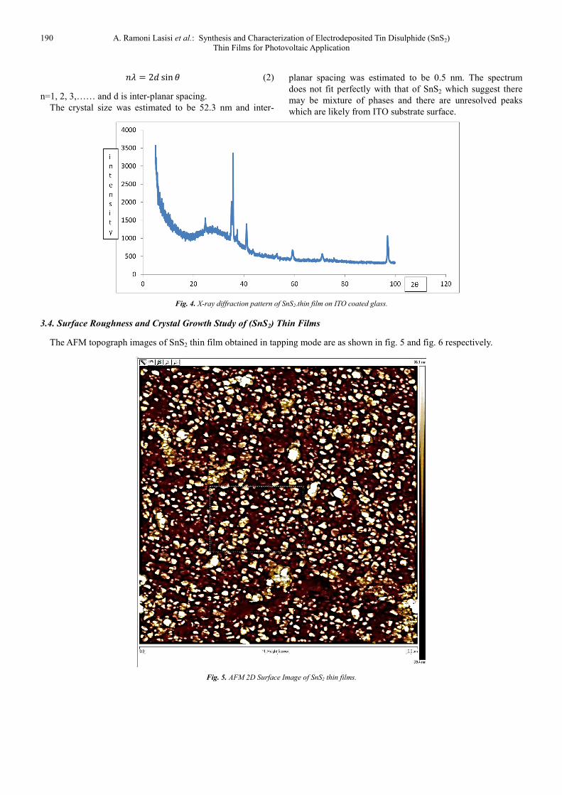
3.4. Surface Roughness and Crystal Growth Study of (SnS2) Thin Films
The AFM topograph images of SnS2 thin film obtained in tapping mode are as shown in fig. 5 and fig. 6 respectively.
Fig. 5. AFM 2D Surface Image of SnS2 thin films.
International Journal of Materials Science and Applications 2016; 5(5): 188-193 191
Fig. 6. AFM Topograph Image of SnS2 thin films.
The two dimension surface image above reveals that the film is uniformly distributed and covered every surface of the substrate with no pin hole and it is crack free. This is consistence with the SEM results. Thus, it can be concluded that a pin hole and crack free SnS2 thin films can be deposited using electrodeposition technique.
From the three dimension topography image of SnS2 thin films, it reveals that the films grains grows perpendicular to the substrate surface, the average crystal growth height is measured to be 90.5 nm and the Root mean square (RMS) surface roughness which is defined as the standard deviation of the surface height profile from average height is given to be 90.2 nm.
3.5. Optical Studies
The data obtained from Uv-visible spectrophotometer were analysed using the following formulae:
h= Planck’s constant, c=speed of light and λ=wavelength an
�&' � ��&' � (�)
* , (6)
n=1 for direct and 4 for indirect band gap. Thus, the Transmittance, Reflectance and Absorbance
spectrum of the film were plot in the visible region and they are as shown below:
Fig. 7. Graph of Transmittance (%) vs Wavelength (nm).
192 A. Ramoni Lasisi et al.: Synthesis and Characterization of Electrodeposited Tin Disulphide (SnS2) Thin Films for Photovoltaic Application
Fig. 8. Graph of Reflectance (%) vs Wavelength (nm).
Fig. 9. Graph of Absorbance (%) vs Wavelength (nm).
The results from fig. 7, 8 and 9 shows that the transmittance of the film in the visible spectrum varies from 53% to 78%, the reflectance varies from 11 to 19% and absorbance varies from 11 to 27% respectively. Thus, the material (SnS2 thin films) is a good transmittance but poor reflector and absorber in the visible region.
Fig. 10. Graph of Energy (eV) Vs α½.
Fig. 11. Graph of Energy (eV) Vs α².
Fig. 10 is a graph of energy (eV) versus square root of α (absorption coefficient). From the graph there is only one critical point which implies that the optical transition is not phonon assisted. Thus, the material is not an indirect band gap material. Fig. 11 is a graph of energy (eV) versus square of α (absorption coefficient). From this graph it shows that the thin film is a direct band gap material with energy band gap of 2.8 eV. This value is quite high compared to 2.12-2.44 eV recorded by [3, 4 and 5]. This may be due to the fact the thin film has not been annealed since annealing usually improve on the crystalinity as well as reduced the optical band gap of material.
4. Conclusion
SnS2 thin films have been electrodeposited from SnSO4, Na2S2O3 and H2SO4 using simple two electrodes electrochemical cells. The thin films were found to be crystalline in nature with hexagonal crystal structure and the particle size is found to be 52.3nm. The material is a direct band gap material with energy band gap of 2.8eV. It is transmittance in the visible is up to 78%. Thus, this material with a wide band gap and high transmittance is suitable for use as window layer in the thin film photovoltaic cells and other optoelectronics devices.
References
[1] C. Nascu, V. Ionescu, E. Indrea, and I. Bratu (1997) Mater. Lett. 32, 73.
[2] J. Touskova, D. Kindl, and J. Tousek (1994) Phys. stat. sol. (a) 142, 539.
[3] A. Sánchez-Juárez, A. Tiburcio-Silver and A. Ortiz (2005) Thin Solid Films 452, 480–481.
[4] L. S. Price, I. P. Parkin, A. M. E. Hardy and R. J. H. Clark. (1999) Chem. Mater. 11, 1792.
[5] C. D. Lokhande (1990) J. Phys. D: Appl. Phys. 23, 1703. 2.5 3.0 3.5 4.0 4.5 5.0
0.050
0.055
0.060
0.065
0.070
0.075
0.080
Alp
ha S
qrt
Energy (eV)
B
2.5 3.0 3.5 4.0 4.5 5.0
0.000005
0.000010
0.000015
0.000020
0.000025
0.000030
0.000035
0.000040
Alp
ha S
quare
Energy (eV)
B
International Journal of Materials Science and Applications 2016; 5(5): 188-193 193
[6] Patil S G and Fredgold R H (1971) J. Phys. D: Appl. Phys. 4, 718.
[7] Said G and Lee P A (1973) Phys. Status Solidi (a) 15 99.
[8] S. K. Panda, A. Antonakos, E. Liarokapis, S. Bhattacharya and S. Chaudhuri (2007) Mater. Res. Bull. 42, 576.
[9] C. Khélia, K. Boubaker, T. B. Nasrallah, M. Amlouk and S. Belgacem (2009) J. Alloys Compd. 461, 477.
[10] N. G. Deshpande, A. A. Sagade, Y. G. Gudage, C. D. Lokhande and R. Sharma (2007) J. Alloys Compd. 421, 436.
[11] J. Malaquinas, P. A. Femandes, P. M. P. Salome, A. F. da Cunba (2011) Thin Solid Films 519, 7416.
[12] C. Shi, Z. Chen, G. Shi, R. Sun, X. Zhan and X. Shen (2012) Thin Solid Films 520, 4898-4901.
[13] L. Amalaraj, C. Sanjjeeviraja and M. Jayachandran (2002) Journal of Crystal Growth 234, 683.